Embed Size (px)
Citation preview

2007.09.13 RFIC WS, A. Matsuzawa
1
Matsuzawa& Okada Lab.Matsuzawa& Okada Lab.
Direction of RF-CMOStuner technology
Akira Matsuzawa
Department of Physical ElectronicsTokyo Institute of Technology

2007.09.13 RFIC WS, A. Matsuzawa
2
Matsuzawa& Okada Lab.Matsuzawa& Okada Lab.
SoC for DVD systems
World first fully integrated mixed signal SoC for DVD systems has developed.
Variable Gain Amp.Variable
Gain Amp.Analog
FilterAnalog
FilterA to D
ConverterA to D
ConverterDigital
FIR FilterDigital
FIR FilterViterbiError
Correction
ViterbiError
Correction
ClockRecoveryClock
RecoveryVoltage
ControlledOscillator
Voltage ControlledOscillatorData In
(Erroneous)
Data Out(No error)
Analog circuit
Digital circuit
Pickup signal
Processed Signal
PixelOperationProcessor
PixelOperationProcessor
IOProcessor
IOProcessor
AVDecode
Processor
AVDecode
Processor
Back -EndBack -End
SystemCont-roller
SystemCont-roller
CPU1CPU1CPU2CPU2
VCOVCO
ADCADC
Gm-CFilterGm-CFilter
PRMLRead
Channel
PRMLRead
ChannelServo DSPServo DSP
AnalogFront EndAnalog
Front End
Front-EndFront-EndAnalog FE+Digital R/C
PixelOperationProcessor
PixelOperationProcessor
IOProcessor
IOProcessor
AVDecode
Processor
AVDecode
Processor
Back -EndBack -End
SystemCont-roller
SystemCont-roller
CPU1CPU1CPU2CPU2
VCOVCO
ADCADC
Gm-CFilterGm-CFilter
PRMLRead
Channel
PRMLRead
ChannelServo DSPServo DSP
AnalogFront EndAnalog
Front End
Front-EndFront-EndAnalog FE+Digital R/C
Okamoto, et. al., ISSCC 2003.0.13um CMOS, 24Mtr
Digital signal processing enables perfect cure for the damaged signals.
Digital read channel technology
DVD
7b, 400MHz, 40mW ADChas been developed
My last work in Panasonic
Before talking about RF-CMOS for tuners

2007.09.13 RFIC WS, A. Matsuzawa
3
Matsuzawa& Okada Lab.Matsuzawa& Okada Lab.
Power of SoC
Model;2000 Model; 2003Before SoC After SoC
SoC has enabled performance increase and cost decrease.Many components and ICs have been kicked out from the PC board.
Panasonic DVD recorder

2007.09.13 RFIC WS, A. Matsuzawa
4
Matsuzawa& Okada Lab.Matsuzawa& Okada Lab.
Contents
• Conventional AM/FM tuner• Analog-centric CMOS tuner• Digital-centric CMOS tuner• Feature of CMOS technology• Conclusion
E-mail: [email protected]: http://www.ssc.pe.titech.ac.jp/
Courtesy Niigata-Seimitsu Co., Ltd.
2007.09.13 RFIC WS, A. Matsuzawa
5
Matsuzawa& Okada Lab.Matsuzawa& Okada Lab.
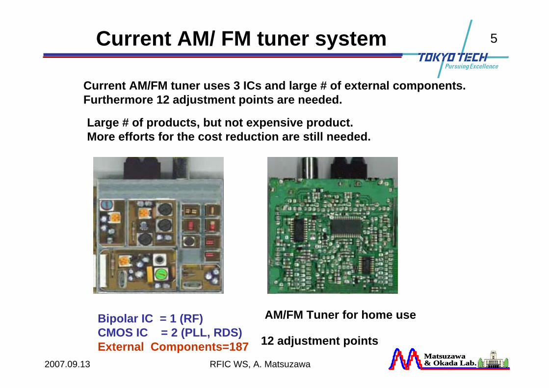
Current AM/ FM tuner system
Bipolar IC = 1 (RF)CMOS IC = 2 (PLL, RDS)External Components=187 12 adjustment points
AM/FM Tuner for home use
Current AM/FM tuner uses 3 ICs and large # of external components.Furthermore 12 adjustment points are needed.
Large # of products, but not expensive product.More efforts for the cost reduction are still needed.
2007.09.13 RFIC WS, A. Matsuzawa
6
Matsuzawa& Okada Lab.Matsuzawa& Okada Lab.
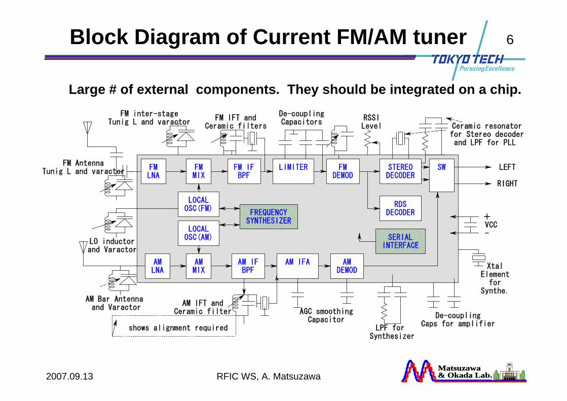
Block Diagram of Current FM/AM tuner
FMLNA
FMMIX
FM IFBPF
LIMITER FMDEMOD
STEREODECODER
LOCALOSC(AM)
LOCALOSC(FM)
AMLNA
AMMIX
AM IFBPF
AM IFA AMDEMOD
SERIALINTERFACE
FREQUENCYSYNTHESIZER
RDSDECODER
SW LEFT
RIGHT
AM Bar Antenna and Varactor
LO inductorand Varactor
AM IFT andCeramic filter
FM AntennaTunig L and varactor
FM inter-stageTunig L and varactor
FM IFT andCeramic filters
De-couplingCapacitors
Ceramic resonatorfor Stereo decoderand LPF for PLL
+
-VCC
De-couplingCaps for amplifier
LPF for Synthesizer
AGC smoothingCapacitor
RSSILevel
XtalElement
forSynthe.
shows alignment required
Large # of external components. They should be integrated on a chip.
2007.09.13 RFIC WS, A. Matsuzawa
7
Matsuzawa& Okada Lab.Matsuzawa& Okada Lab.
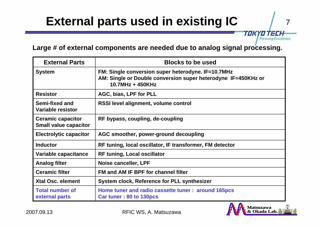
External parts used in existing IC
System clock, Reference for PLL synthesizerXtal Osc. element
FM: Single conversion super heterodyne. IF=10.7MHzAM: Single or Double conversion super heterodyne IF=450KHz or
10.7MHz + 450KHz
System
RSSI level alignment, volume controlSemi-fixed and Variable resistor
RF tuning, Local oscillatorVariable capacitance
Home tuner and radio cassette tuner : around 165pcsCar tuner : 80 to 130pcs
Total number of external parts
FM and AM IF BPF for channel filter Ceramic filterNoise canceller, LPFAnalog filter
RF tuning, local oscillator, IF transformer, FM detectorInductor
AGC smoother, power-ground decouplingElectrolytic capacitor
RF bypass, coupling, de-coupling Ceramic capacitorSmall value capacitor
AGC, bias, LPF for PLLResistor
Blocks to be usedExternal Parts
Large # of external components are needed due to analog signal processing.
2007.09.13 RFIC WS, A. Matsuzawa
8
Matsuzawa& Okada Lab.Matsuzawa& Okada Lab.
Issues and conventional solutions of AM/FM tuner
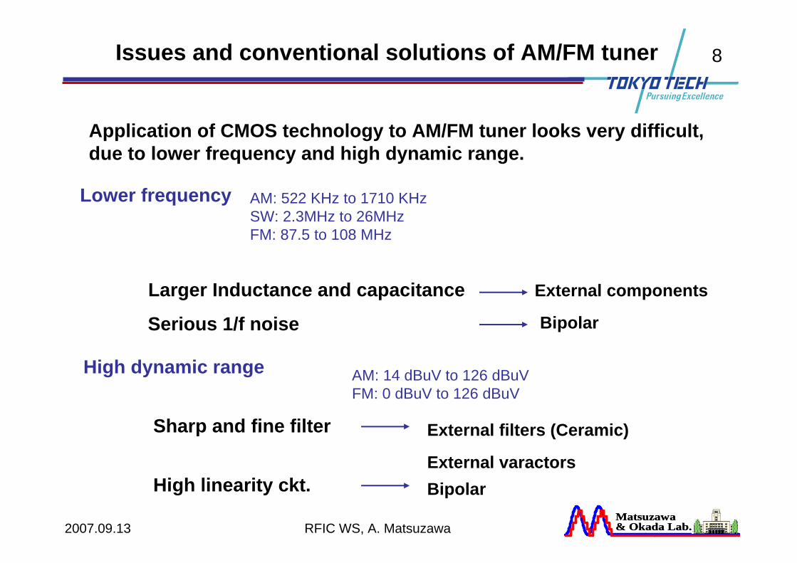
Lower frequency AM: 522 KHz to 1710 KHzSW: 2.3MHz to 26MHzFM: 87.5 to 108 MHz
Larger Inductance and capacitance
High dynamic range
Serious 1/f noise
Sharp and fine filter
AM: 14 dBuV to 126 dBuVFM: 0 dBuV to 126 dBuV
High linearity ckt.
Bipolar
External components
External filters (Ceramic)
External varactorsBipolar
Application of CMOS technology to AM/FM tuner looks very difficult,due to lower frequency and high dynamic range.
2007.09.13 RFIC WS, A. Matsuzawa
9
Matsuzawa& Okada Lab.Matsuzawa& Okada Lab.
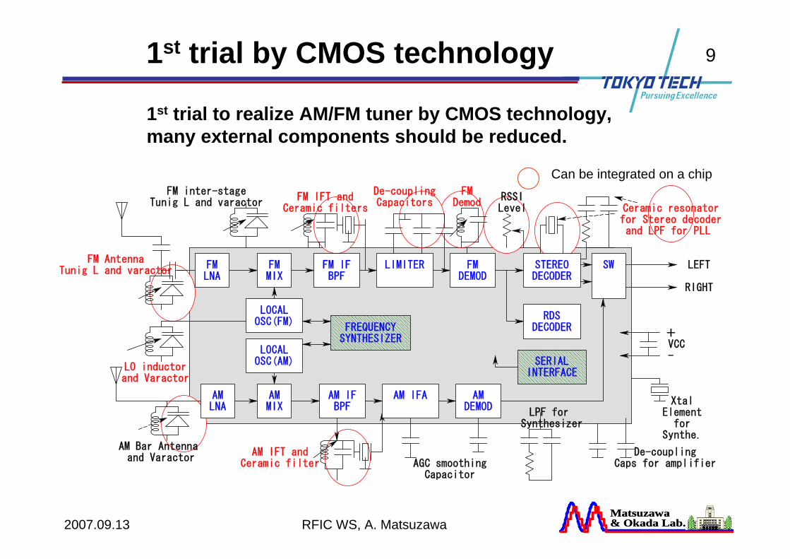
1st trial by CMOS technology
FMLNA
FMMIX
FM IFBPF
LIMITER FMDEMOD
STEREODECODER
LOCALOSC(AM)
LOCALOSC(FM)
AMLNA
AMMIX
AM IFBPF
AM IFA AMDEMOD
SERIALINTERFACE
FREQUENCYSYNTHESIZER
RDSDECODER
SW LEFT
RIGHT
AM Bar Antenna and Varactor
FM inter-stageTunig L and varactor
+
-VCC
AGC smoothingCapacitor
RSSILevel
XtalElement
forSynthe.
FMDemod
FM IFT andCeramic filters
AM IFT andCeramic filter
De-couplingCapacitors
Ceramic resonatorfor Stereo decoderand LPF for PLL
FM AntennaTunig L and varactor
LO inductorand Varactor
LPF for Synthesizer
De-couplingCaps for amplifier
Can be integrated on a chip
1st trial to realize AM/FM tuner by CMOS technology,many external components should be reduced.
2007.09.13 RFIC WS, A. Matsuzawa
10
Matsuzawa& Okada Lab.Matsuzawa& Okada Lab.
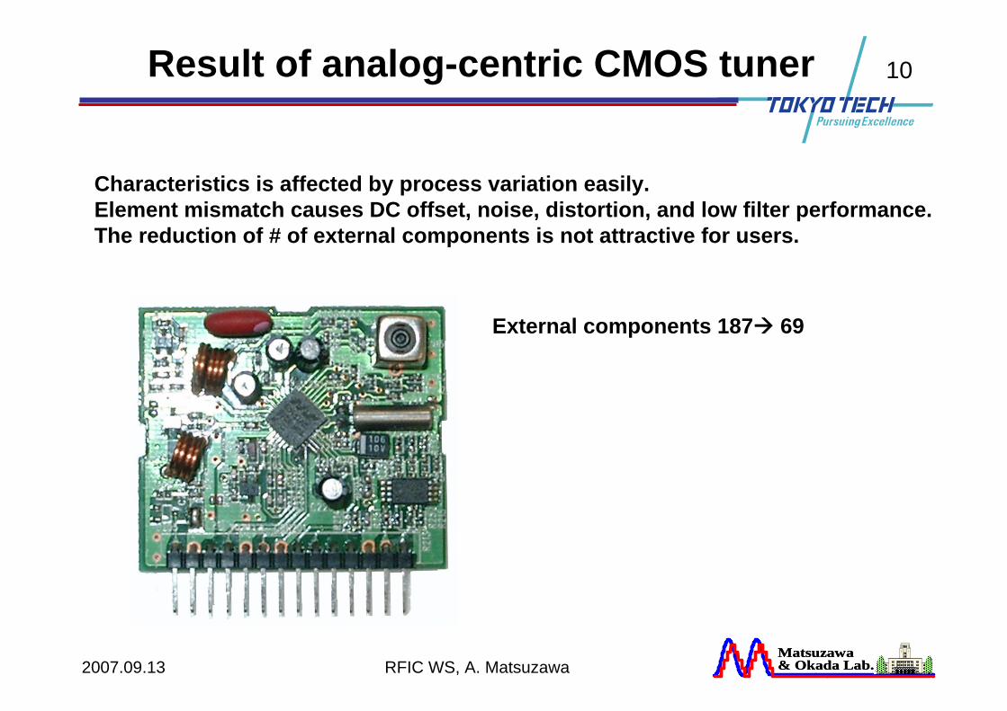
Result of analog-centric CMOS tuner
External components 187 69
Characteristics is affected by process variation easily.Element mismatch causes DC offset, noise, distortion, and low filter performance.The reduction of # of external components is not attractive for users.

2007.09.13 RFIC WS, A. Matsuzawa
11
Matsuzawa& Okada Lab.Matsuzawa& Okada Lab.
Analog-centric CMOS tuner technology
Needs large capacitor for low audio frequency
Time division charge and dischargeAGC smoother
ProblemsMethods for on-chipParts
Poor THD (0.5%)Pulse count FM detectorFM Demodulator
1.poor selectivity(-45dB), 2. SCF Switch noise 3. Center frequency shift by DC offset4. Poor image rejection ratio (25 to 35dB)
1. Low IF( a few hundred KHz)2.Gm-C BPF with auto alignment, SCF
AM/FM IF BPF
High impedance required, Difficult for low frequency
Stages Direct connection, use small value coupling capacitor
Capacitors
Too much sharp C-V curve, distorted signal
MOS varactorVaractor
Can’t cover all process cornerSignal detector with DC compensation
RSSI Level adj.
Large variation of free-run frequencyStill need external LPF for PLL
Multi-vibrator VCO, SCF filter Stereo Decoder
1st trial was analog-centric CMOS tuner technology.
Circuits have been replaced by CMOS, however still use analog technology.Thus it had many issues and many external components were still needed.
2007.09.13 RFIC WS, A. Matsuzawa
12
Matsuzawa& Okada Lab.Matsuzawa& Okada Lab.
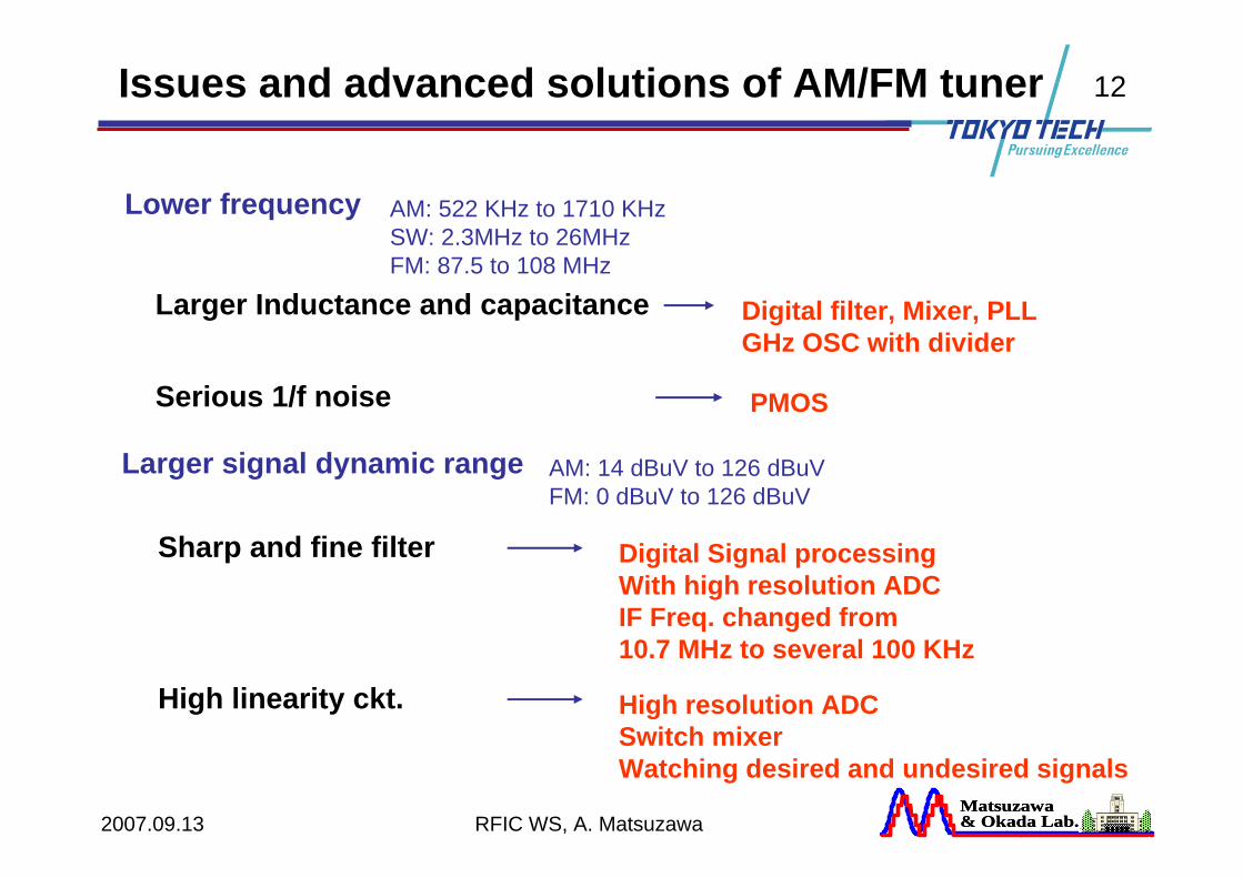
Issues and advanced solutions of AM/FM tuner
Lower frequency AM: 522 KHz to 1710 KHzSW: 2.3MHz to 26MHzFM: 87.5 to 108 MHz
Larger Inductance and capacitance
Larger signal dynamic range
Serious 1/f noise
Sharp and fine filter
AM: 14 dBuV to 126 dBuVFM: 0 dBuV to 126 dBuV
High linearity ckt.
PMOS
Digital filter, Mixer, PLLGHz OSC with divider
High resolution ADCSwitch mixerWatching desired and undesired signals
Digital Signal processingWith high resolution ADCIF Freq. changed from 10.7 MHz to several 100 KHz

2007.09.13 RFIC WS, A. Matsuzawa
13
Matsuzawa& Okada Lab.Matsuzawa& Okada Lab.
Advanced CMOS tuner
FMLNA
+
-
FMMIX
Anti-AliasLPF
VGA ADC DAC
LOCALOSC(FM)
FREQUENCYSYNTHESIZER
AMLNA
SERIALINTERFACE
REGISTER
Cap.Array
AM Bar Antenna(No need for Car radio)
AGC
AGC
AGC
AGC
FM Tuneor BPF
Xtal
XOSC
SYSCLKGEN
PowerDecoupling
Cap
VCC
DSP
STEREODECODER
FMIFBPF
FMDEMOD
RDSDEC
DECI.LPF
AGC GENERATOR
AMMIX
AMIFBPF
AMDEMOD
DIGITALAM LO
To/FromMPU
LEFT
RIGHTCap.Array
Digital-centric CMOS tuner has been developed.
2007.09.13 RFIC WS, A. Matsuzawa
14
Matsuzawa& Okada Lab.Matsuzawa& Okada Lab.
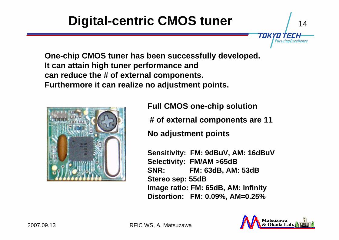
Digital-centric CMOS tuner
Full CMOS one-chip solution# of external components are 11
No adjustment points
Sensitivity: FM: 9dBuV, AM: 16dBuVSelectivity: FM/AM >65dBSNR: FM: 63dB, AM: 53dBStereo sep: 55dBImage ratio: FM: 65dB, AM: InfinityDistortion: FM: 0.09%, AM=0.25%
One-chip CMOS tuner has been successfully developed.It can attain high tuner performance andcan reduce the # of external components.Furthermore it can realize no adjustment points.
2007.09.13 RFIC WS, A. Matsuzawa
15
Matsuzawa& Okada Lab.Matsuzawa& Okada Lab.
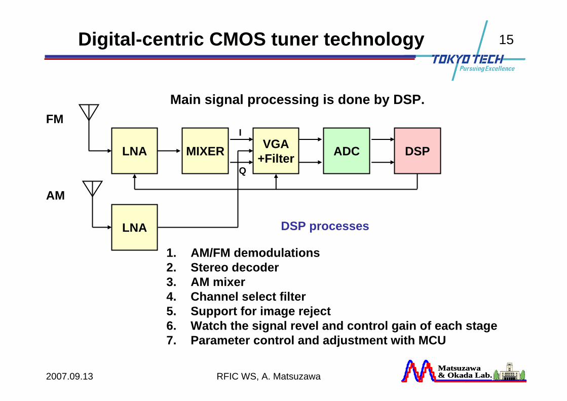
Digital-centric CMOS tuner technology
ADC DSPVGA+FilterMIXERLNA
LNA
FM
AM
DSP processes
I
Q
1. AM/FM demodulations2. Stereo decoder3. AM mixer4. Channel select filter5. Support for image reject6. Watch the signal revel and control gain of each stage7. Parameter control and adjustment with MCU
Main signal processing is done by DSP.

2007.09.13 RFIC WS, A. Matsuzawa
16
Matsuzawa& Okada Lab.Matsuzawa& Okada Lab.
Demodulation of AM/FM signal
cω
xReceivedsignal
[ ] ( ) ( ) )(1expexp)(1 tStjtjtS cc +=ω−×ω⋅+
Demodulatedsignal
1) AM demodulation
2) FM demodulation
( ) eredrebetosignalBasebandmiationAmplitudetR
offsetFrequency
cov:var:)(
:
τ
ωΔ
I
Q
( )∫ ττ+ωΔ dmjKtjtR d )(exp)(
∫ ττ+ωΔ=θ dmKt d )(θ
dtdθ
)(tmKdtd
d+ωΔ=θ
AM/ FM signals can be demodulated by simple arithmetic operations
)(tR
m(t) can be demodulated
2007.09.13 RFIC WS, A. Matsuzawa
17
Matsuzawa& Okada Lab.Matsuzawa& Okada Lab.
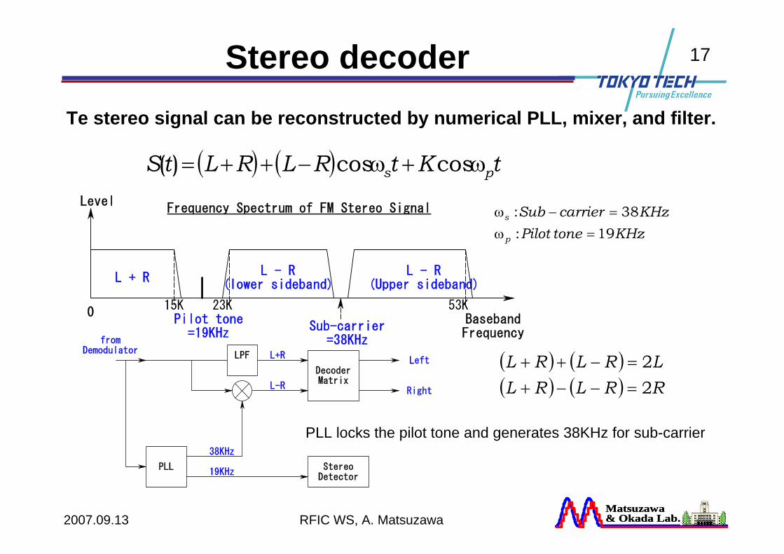
Stereo decoder
Level
L + R
0
L - R(lower sideband)
Sub-carrier=38KHz
L - R(Upper sideband)
Frequency Spectrum of FM Stereo Signal
Pilot tone=19KHz
15K 23KBasebandFrequency
53K
( ) ( ) tKtRLRLtS ps ω+ω−++= coscos)(
KHztonePilotKHzcarrierSub
p
s
19:38:
=ω=−ω
PLL StereoDetector
38KHz
19KHz
Left
Right
DecoderMatrix
fromDemodulator
LPF L+R
L-R
( ) ( )( ) ( ) RRLRL
LRLRL22
=−−+=−++
PLL locks the pilot tone and generates 38KHz for sub-carrier
Te stereo signal can be reconstructed by numerical PLL, mixer, and filter.
2007.09.13 RFIC WS, A. Matsuzawa
18
Matsuzawa& Okada Lab.Matsuzawa& Okada Lab.
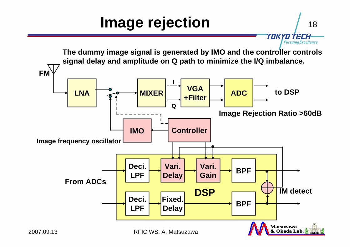
Image rejection
ADCVGA+FilterMIXERLNA
FMI
Q
Deci.LPF
Vari.Delay
Vari.Gain BPF
IMO Controller
Deci.LPF
Fixed.Delay BPF
DSP
to DSP
From ADCs
Image frequency oscillator
IM detect
Image Rejection Ratio >60dB
The dummy image signal is generated by IMO and the controller controls signal delay and amplitude on Q path to minimize the I/Q imbalance.
2007.09.13 RFIC WS, A. Matsuzawa
19
Matsuzawa& Okada Lab.Matsuzawa& Okada Lab.
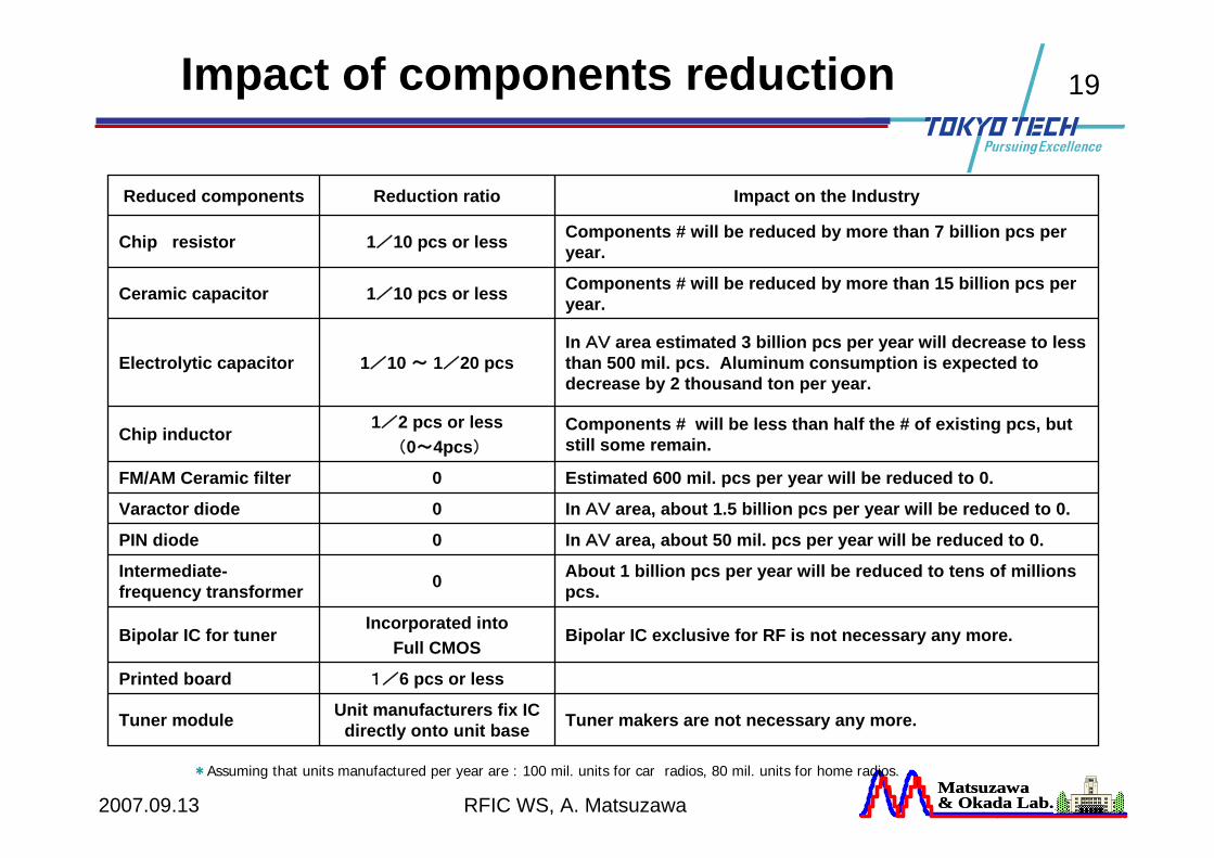
Impact of components reduction
1/6 pcs or lessPrinted board
Tuner makers are not necessary any more.Unit manufacturers fix IC directly onto unit baseTuner module
Bipolar IC exclusive for RF is not necessary any more.
About 1 billion pcs per year will be reduced to tens of millionspcs.
In AV area, about 50 mil. pcs per year will be reduced to 0.
In AV area, about 1.5 billion pcs per year will be reduced to 0.
Estimated 600 mil. pcs per year will be reduced to 0.
Components # will be less than half the # of existing pcs, but still some remain.
In AV area estimated 3 billion pcs per year will decrease to less than 500 mil. pcs. Aluminum consumption is expected to decrease by 2 thousand ton per year.
Components # will be reduced by more than 15 billion pcs per year.
Components # will be reduced by more than 7 billion pcs per year.
Impact on the Industry
Incorporated into Full CMOS
0
0
0
0
1/2 pcs or less(0~4pcs)
1/10 ~ 1/20 pcs
1/10 pcs or less
1/10 pcs or less
Reduction ratio
Bipolar IC for tuner
Intermediate-frequency transformer
PIN diode
Varactor diode
FM/AM Ceramic filter
Chip inductor
Electrolytic capacitor
Ceramic capacitor
Chip resistor
Reduced components
*Assuming that units manufactured per year are : 100 mil. units for car radios, 80 mil. units for home radios.
2007.09.13 RFIC WS, A. Matsuzawa
20
Matsuzawa& Okada Lab.Matsuzawa& Okada Lab.
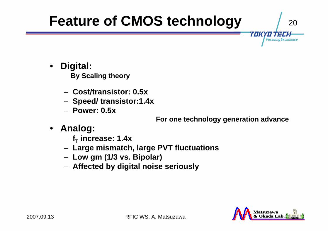
Feature of CMOS technology
• Digital: By Scaling theory
– Cost/transistor: 0.5x – Speed/ transistor:1.4x – Power: 0.5x
• Analog:– fT increase: 1.4x– Large mismatch, large PVT fluctuations– Low gm (1/3 vs. Bipolar) – Affected by digital noise seriously
For one technology generation advance
2007.09.13 RFIC WS, A. Matsuzawa
21
Matsuzawa& Okada Lab.Matsuzawa& Okada Lab.
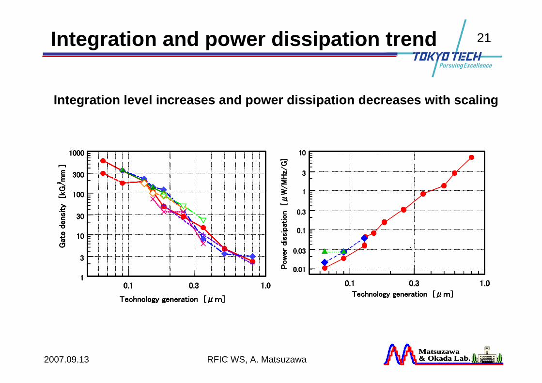
Integration and power dissipation trend
0.1 0.3 1.01
3
10
30
100
300
1000
Technology generation [μm]
Gat
e d
ensi
ty[k
G/m
m ]
2
0.1 0.3 1.01
3
10
30
100
300
1000
Technology generation [μm]
Gat
e d
ensi
ty[k
G/m
m ]
2
0.1 0.3 1.0
0.01
0.03
0.1
0.3
1
3
10
Technology generation [μm]
Pow
er
dis
sipat
ion
[μW
/M
Hz/
G]
0.1 0.3 1.0
0.01
0.03
0.1
0.3
1
3
10
Technology generation [μm]
Pow
er
dis
sipat
ion
[μW
/M
Hz/
G]
Integration level increases and power dissipation decreases with scaling

2007.09.13 RFIC WS, A. Matsuzawa
22
Matsuzawa& Okada Lab.Matsuzawa& Okada Lab.
Feature of Analog CMOS technology
• Pros– Can use switch and voltage controlled conductance– Smaller distortion– No carrier accumulation – Can use switched capacitor circuits– Can increase fT by scaling– Easy use of complementally circuits– Easy integration with digital circuits
• Cons– Low gm/Ids– Larger mismatch voltage and 1/f noise– Lower operating voltage with scaling– Difficult to enable impedance matching– Easily affected by substrate
Akira Matsuzawa, “Mixed Signal SoC Era,” IEICE, Trans. Electron., Vol. E87-c, No. 6, pp. 867-877, June, 2004.
2007.09.13 RFIC WS, A. Matsuzawa
23
Matsuzawa& Okada Lab.Matsuzawa& Okada Lab.
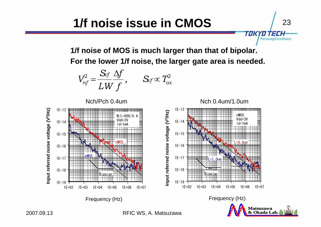
1/f noise issue in CMOS
1E-19
1E-18
1E-17
1E-16
1E-15
1E-14
1E-13
1E+02 1E+03 1E+04 1E+05 1E+06 1E+07
L=0.4um
L=1.0um
Bipolar
nMOSVdd=3VId=1mA
1E-19
1E-18
1E-17
1E-16
1E-15
1E-14
1E-13
1E+02 1E+03 1E+04 1E+05 1E+06 1E+07
nMOS
pMOS
W/L=800/0.4Vdd=3VId=1mA
Bipolar
2
Inpu
t ref
erre
d no
ise
volta
ge (V
2 /Hz)
Frequency (Hz) Frequency (Hz)
Inpu
t ref
erre
d no
ise
volta
ge (V
2 /Hz)
Nch/Pch 0.4um Nch 0.4um/1.0um
1/f noise of MOS is much larger than that of bipolar.
22 , oxvfvf
nf TSff
LWSV ∝
Δ=
For the lower 1/f noise, the larger gate area is needed.
2007.09.13 RFIC WS, A. Matsuzawa
24
Matsuzawa& Okada Lab.Matsuzawa& Okada Lab.
Why CMOS?
• Low cost– Must be biggest motivation– CMOS is 30-40% lower than Bi-CMOS
• High level system integration– CMOS is one or two generation advanced– CMOS can realize full system integration
• Stable supplyment and multi-foundries– Fabs for SiGe-BiCMOS are very limited.
Slow price decrease and limited product capability
• Easy to use– Universities and start-up companies can use CMOS with
low usage fee, but SiGe is difficult to use such programs.

2007.09.13 RFIC WS, A. Matsuzawa
25
Matsuzawa& Okada Lab.Matsuzawa& Okada Lab.
Is CMOS cheaper?
0
500
1000
1500
2000
2500
3000
3500
4000
4500
0.35
_C
0.25
_C0.
25Si
Ge_
BC0.
25_S
iGe_
BC0.
18um
_C0.
15um
_C0.
13um
_C7M
6M
5M
4M
3M
Low costSiGe
45%45% 23%
30%
Dataquest March 2001+SiGe estimation
Wafer cost of SiGe BiCMOS is 30-40% higher than CMOS at the same generation,however almost same as one generation advanced CMOS.

2007.09.13 RFIC WS, A. Matsuzawa
26
Matsuzawa& Okada Lab.Matsuzawa& Okada Lab.
Cost up issue by analog parts
0
0.1
0.2
0.3
0.4
0.5
0.6
0.7
0.8
0.9
1
0.35um 0.25um 0.18um 0.13um0
0.1
0.2
0.3
0.4
0.5
0.6
0.7
0.8
0.9
1
0.35um 0.25um 0.18um 0.13um
(0.35um : 1)
Chip area Chip cost
I/OAnalog
Digital
Cost of mixed A/D LSI will increase when using deep sub-micron device, due to the increase of cost of non-scalable analog parts.
Large analog may be unacceptable.Some analog circuits should be replaced by digital circuits
Wafer cost increases 1.3xfor one generation
Akira Matsuzawa, “RF-SoC- Expectations and Required Conditions,”IEEE Tran. On Microwave Theory and Techniques, Vol. 50, No. 1, pp. 245-253, Jan. 2002
2007.09.13 RFIC WS, A. Matsuzawa
27
Matsuzawa& Okada Lab.Matsuzawa& Okada Lab.
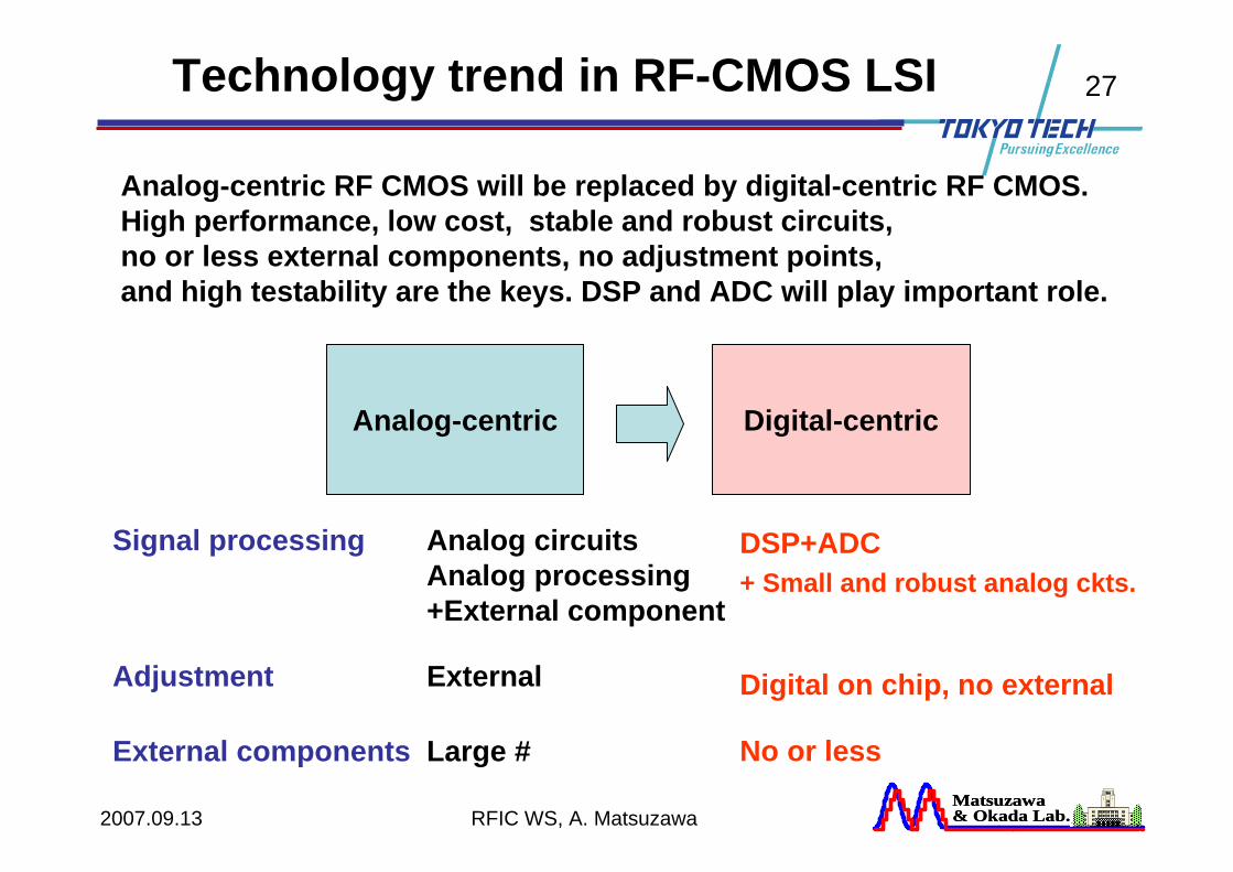
Technology trend in RF-CMOS LSI
Analog-centric Digital-centric
Analog circuitsAnalog processing+External component
Signal processing DSP+ADC+ Small and robust analog ckts.
Adjustment External Digital on chip, no external
External components Large # No or less
Analog-centric RF CMOS will be replaced by digital-centric RF CMOS.High performance, low cost, stable and robust circuits, no or less external components, no adjustment points, and high testability are the keys. DSP and ADC will play important role.

2007.09.13 RFIC WS, A. Matsuzawa
28
Matsuzawa& Okada Lab.Matsuzawa& Okada Lab.
Technology trend in RF CMOS LSI
M. Zargari (Atheros), et al., ISSCC 2004, pp.96 K. Muhammad (TI), et al., ISSCC2004, pp.268
Discrete-time Bluetooth0.13um, 1.5V, 2.4GHz
Wireless LAN, 802.11 a/b/g0.25um, 2.5V, 23mm2, 5GHz
Analog centric RF CMOS will be replaced by digital centric RF CMOS.
2007.09.13 RFIC WS, A. Matsuzawa
29
Matsuzawa& Okada Lab.Matsuzawa& Okada Lab.
Wide-band delta-sigma ADC
50mW (analog), 6mW (digital)Power consumption
1.2VSupply voltage
71dB / 69dBPeak SNR / SNDR*
0.2pJ/conv. (FOM=P/(2^enob*2*BW))Figure-of-merit (FOM)
77dB (97dB @ 200kHz, 115dB @ 3kHz)Dynamic range*
0.5mm2Active chip area
>55dB (for -1MHz input tone)Image rejection
1Vp (differential)Max. input voltage
20MHz @ 10.5MHz IFBandwidth
340MHzSampling frequency
CT quadrature cascaded ΣΔ modulator (2-2, 4b)Architecture
90nm CMOS, 1P6MTechnology
(*1MHz input signal, signal bandwidth is 20MHz)
90nm CMOS、BW=20MHz, DR(=SNR)=77dB, 50mmW, FoM=200fJ/conv.AD
C1i
ADC
2i
DAC2iDAC1i DAC3i
DAC1q
ADC
1q
DAC2q DAC3q
ADC
2q
+
+-
- +
+-
- +
+-
- +
+-
-
+
+-
-+
+-
-+
+-
-+
+-
-
R2iR1i R3i R4i
R5i R6i R7i R8i
R5q R6q R7q R8q
R2qR1q R3q R4q
C1i C2i C3i C4i C5i C6i
C1q C2q C3q C4q C5q C6q
4b 4b
4b 4b
Vpi
Vmi
Vpq
Vmq
Y1i Y2i
Y1q Y2q
ADC
1i
ADC
2i
DAC2iDAC1i DAC3i
DAC1q
ADC
1q
DAC2q DAC3q
ADC
2q
+
+-
- +
+-
- +
+-
- +
+-
-
+
+-
-+
+-
-+
+-
-+
+-
-
R2iR1i R3i R4i
R5i R6i R7i R8i
R5q R6q R7q R8q
R2qR1q R3q R4q
C1i C2i C3i C4i C5i C6i
C1q C2q C3q C4q C5q C6q
4b 4b
4b 4b
Vpi
Vmi
Vpq
Vmq
Y1i Y2i
Y1q Y2q
L. J. Breems, et., al. “A 56mW CT Quadrature Cascaded SD Modulatorwith 77dB in a Near aero-IF 20MHz Band.ISSCC 2007, pp. 238-239.
Wide band and high dynamic range delta-sigma ADC is the key for digital centric systems
2007.09.13 RFIC WS, A. Matsuzawa
30
Matsuzawa& Okada Lab.Matsuzawa& Okada Lab.
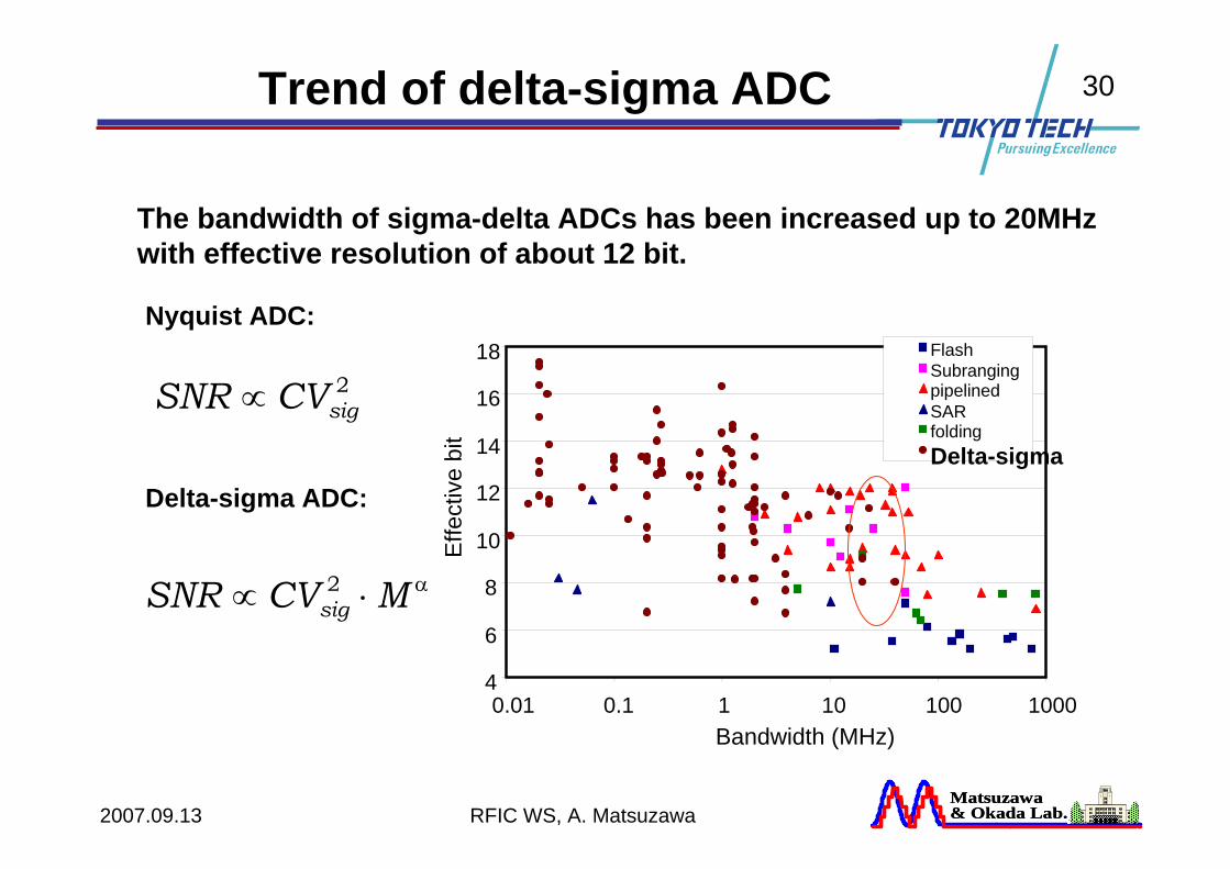
Trend of delta-sigma ADC
4
6
8
10
12
14
16
18
0.01 0.1 1 10 100 1000
FlashSubrangingpipelinedSARfoldingDelta-sigma
Nyquist ADC:
2sigCVSNR ∝
Delta-sigma ADC:
α⋅∝ MCVSNR sig2
The bandwidth of sigma-delta ADCs has been increased up to 20MHzwith effective resolution of about 12 bit.
Effe
ctiv
e bi
t
Bandwidth (MHz)

2007.09.13 RFIC WS, A. Matsuzawa
31
Matsuzawa& Okada Lab.Matsuzawa& Okada Lab.
Conclusion
• Radio tuners have not been replaced by CMOS technology in contrast to many other wireless systems; cellular phones and wireless LANs have been replaced by CMOS.– Low frequency:
• External large L and C, Filters• 1/f noise
– High dynamic range: • External sharp and fine tuning filters
• Analog-centric CMOS technology is not effective– No attractive performance and affected by PVT fluctuation seriously.– Cost increase for further technology scaling– Still need large # of external components and adjusting points
• Digital-centric CMOS technology must be right way– High performance and very robust against PVT fluctuations– Further performance increase and cost reduction are expected by using more
scaled technology– No or less external components and no adjustment points