Embed Size (px)
Citation preview
DM5885 720H Decoder Mix 4 NTSC/PAL Channels to One SD or HD Signal
Final 1
Doc No: DM5885-DS-F01
September 14, 2017
DAVICOM Semiconductor, Inc.
DM5885
720H Decoder Mix 4 NTSC/PAL Channels to One SD or HD Signal
DATA SHEET
Final
Version: DM5885-DS-F01
September 14, 2017
DM5885 720H Decoder Mix 4 NTSC/PAL Channels to One SD or HD Signal
Final 2
Doc No: DM5885-DS-F01
September 14, 2017
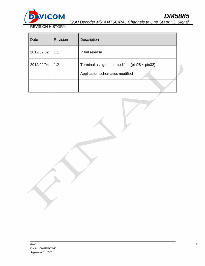
REVISION HISTORY:
Date Revision Description
2012/02/02 1.1 Initial release
2012/02/04 1.2 Terminal assignment modified (pin28 ~ pin32)
Application schematics modified
DM5885 720H Decoder Mix 4 NTSC/PAL Channels to One SD or HD Signal
Final 3
Doc No: DM5885-DS-F01
September 14, 2017
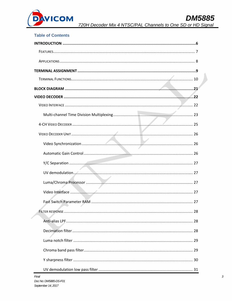
Table of Contents
INTRODUCTION .....................................................................................................................6
FEATURES ....................................................................................................................................... 7
APPLICATIONS ................................................................................................................................. 8
TERMINAL ASSIGNMENT ........................................................................................................9
TERMINAL FUNCTIONS .................................................................................................................... 10
BLOCK DIAGRAM ................................................................................................................. 21
VIDEO DECODER .................................................................................................................. 22
VIDEO INTERFACE .......................................................................................................................... 22
Multi-channel Time Division Multiplexing ............................................................................ 23
4-CH VIDEO DECODER ................................................................................................................... 25
VIDEO DECODER UNIT .................................................................................................................... 26
Video Synchronization .......................................................................................................... 26
Automatic Gain Control ........................................................................................................ 26
Y/C Separation ...................................................................................................................... 27
UV demodulation .................................................................................................................. 27
Luma/Chroma Processor ...................................................................................................... 27
Video Interface ..................................................................................................................... 27
Fast Switch Parameter RAM ................................................................................................. 27
FILTER RESPONSE ........................................................................................................................... 28
Anti-alias LPF ......................................................................................................................... 28
Decimation filter ................................................................................................................... 28
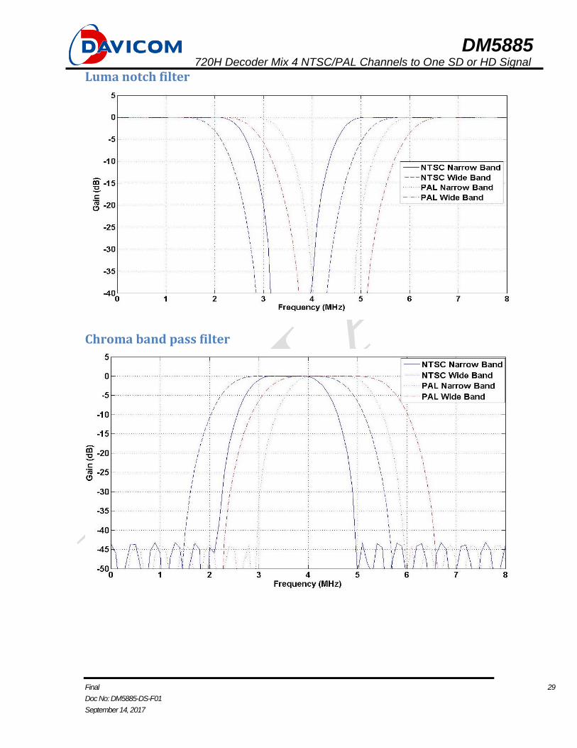
Luma notch filter .................................................................................................................. 29
Chroma band pass filter ........................................................................................................ 29
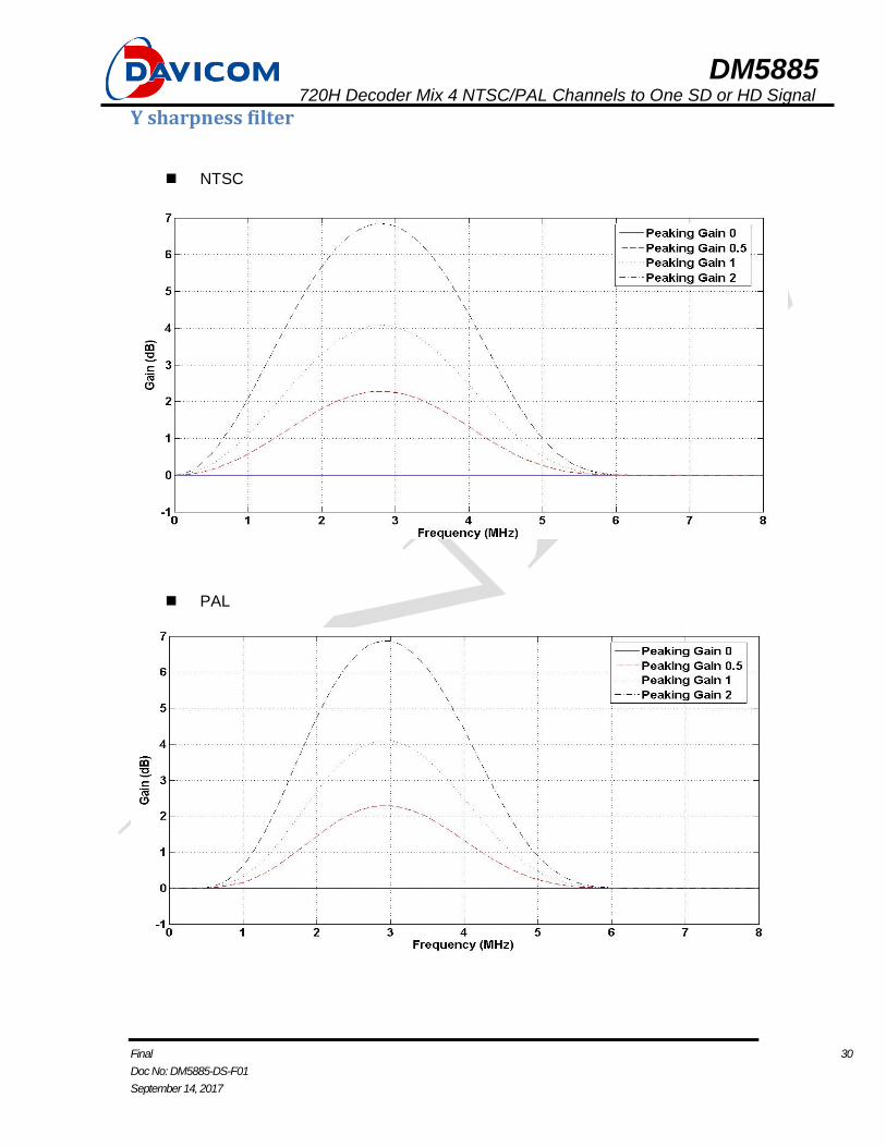
Y sharpness filter .................................................................................................................. 30
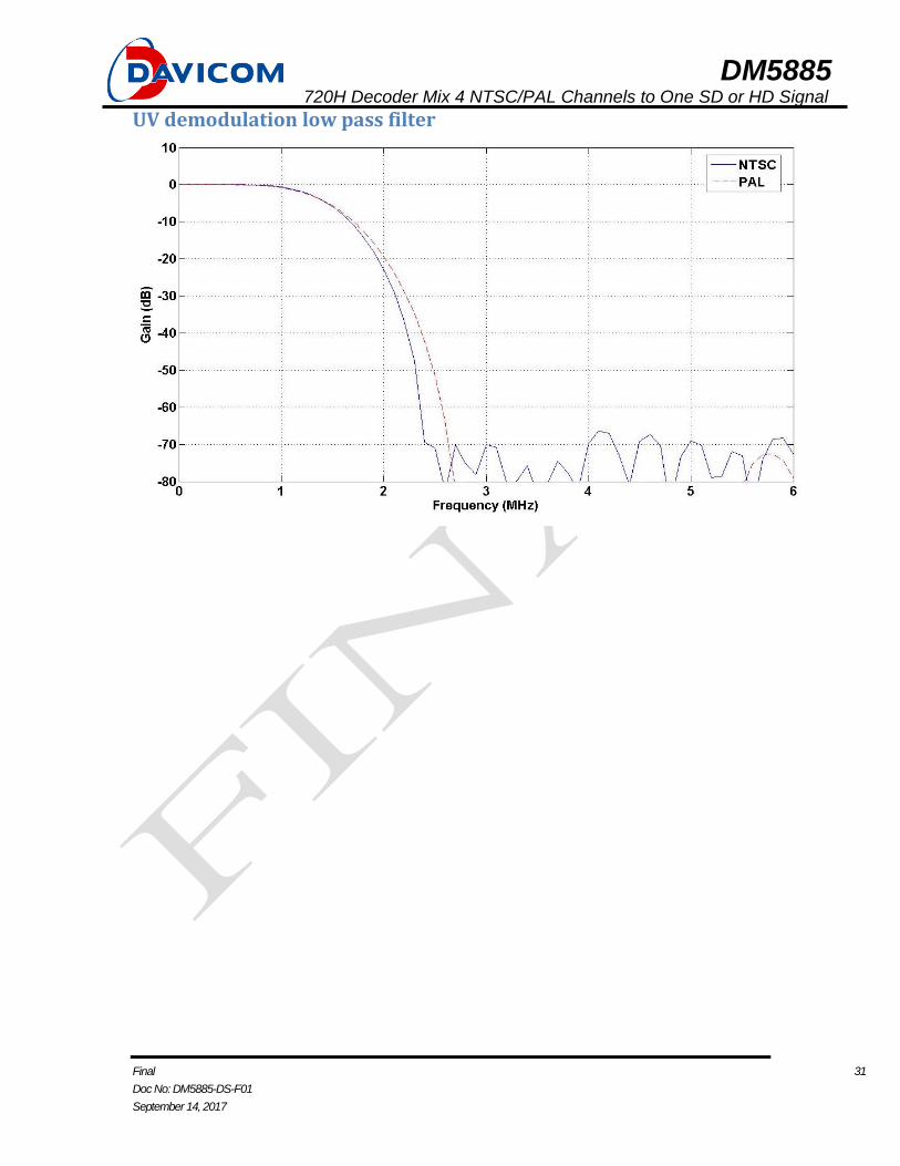
UV demodulation low pass filter .......................................................................................... 31
DM5885 720H Decoder Mix 4 NTSC/PAL Channels to One SD or HD Signal
Final 4
Doc No: DM5885-DS-F01
September 14, 2017
AUDIO CODEC ...................................................................................................................... 32
DIGITAL AUDIO FORMAT ................................................................................................................. 34
EXTENDED DIGITAL AUDIO FORMAT ................................................................................................. 35
PLL ...................................................................................................................................... 36
HOST INTERFACE .................................................................................................................. 37
VIDEO MIXER ....................................................................................................................... 38
OUTPUT FORMAT .......................................................................................................................... 39
VIDEO MIXER BLOCK ...................................................................................................................... 40
Video Source ......................................................................................................................... 40
Channel Switch Block ............................................................................................................ 40
Capture interface .................................................................................................................. 41
Mixer Core ............................................................................................................................ 46
Mix-Out Interface ................................................................................................................. 46
Chip-Level Output Unit ......................................................................................................... 51
INTERNAL CONTROL REGISTERS ............................................................................................ 52
SYSTEM CONTROL .......................................................................................................................... 52
VIDEO ADC .................................................................................................................................. 65
PLL ............................................................................................................................................. 72
AUDIO ADC/DAC ......................................................................................................................... 75
VIDEO DECODER ............................................................................................................................ 83
AGC ....................................................................................................................................... 84
Video Detection Misc ............................................................................................................ 85
Color Killer ............................................................................................................................ 86
2D Comb Filter ...................................................................................................................... 86
VIDEO MIXER .............................................................................................................................. 109
MIXER OUTSEL CONFIGURATION TABLE .............................................................................. 132
DM5885 720H Decoder Mix 4 NTSC/PAL Channels to One SD or HD Signal
Final 5
Doc No: DM5885-DS-F01
September 14, 2017
ELECTRICAL SPECIFICATIONS .............................................................................................. 137
ABSOLUTE MAXIMUM RATINGS OVER OPERATING FREE-AIR TEMPERATURE RANGE .............................. 137
Recommended Operating Conditions ................................................................................ 138
Crystal Specifications .......................................................................................................... 139
ELECTRICAL CHARACTERISTICS ........................................................................................................ 139
DC ELECTRICAL CHARACTERISTICS .................................................................................................. 139
Analog Processing and A/D Converters .............................................................................. 140
Timing ................................................................................................................................. 140
PACKAGING ....................................................................................................................... 144
ORDERING INFORMATION.................................................................................................. 145
DISCLAIMER .............................................................................................................................. 145
PRODUCTS ............................................................................................................................... 145
CONTACT WINDOWS ................................................................................................................. 145
DM5885 720H Decoder Mix 4 NTSC/PAL Channels to One SD or HD Signal
Final 6
Doc No: DM5885-DS-F01
September 14, 2017
Introduction
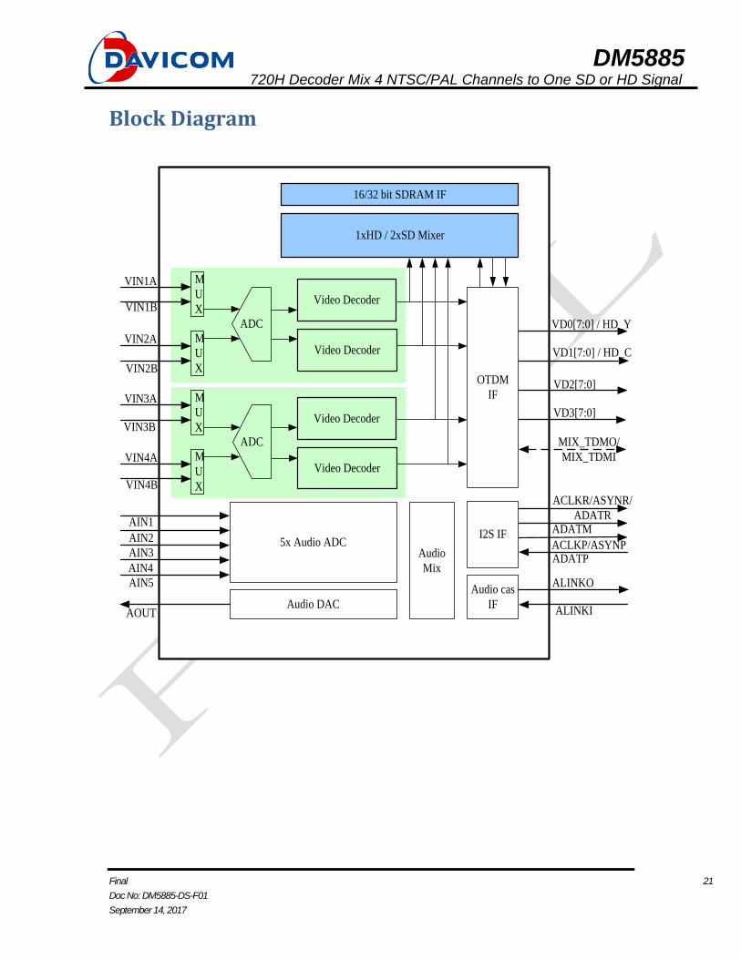
The DM5885 is a 4-channel video decoder which converts 4 channels of 6.5 MHz analog
CVBS signals to 4 channels of digital 27 MHz CCIR656 signals. The DM5885 integrates
two internal PLLs, and decodes 720H videos using the same (27MHz) external clock
source. The DM5885 also features a patented fast switch function. With the fast switch
function, the DM5885 can decode up to 8 analog CVBS with little frame rate loss.
The DM5885 includes two SD mixers and one HD mixer. Each SD/HD mixer can
multiplex up to 4 video sources. In addition to two SD CCIR656 outputs or one HD
SMPTE 274M output, the DM5885 mixer can output four D1 videos through one TDM4
interface. The mixers support image mirror and H partition functions. Both interlaced and
progressive digital video outputs are supported.
The DM5885 also includes five audio ADCs and one audio DAC.
DM5885 720H Decoder Mix 4 NTSC/PAL Channels to One SD or HD Signal
Final 7
Doc No: DM5885-DS-F01
September 14, 2017
Features
Video Decoder
Accepts NTSC (M,J), PAL (B, D, G, H, I, M, Nc)
Hardware Fast Switch function
Fast Switch also controllable by software or external pin
Software channel ID in active region
Four 10-bits video ADCs with built in 6.5 MHz analog low pass filter
Automatic gain control for Luminance and Chrominance
Programmable brightness, contrast, saturation, hue, and sharpness
5-H comb filter for YC separation
Chrominance line filter for PAL phase error
DLL for video synchronization, supports 27MHz crystal within +/-1000 ppm variance
Advanced video synchronization for weak and noisy CVBS. Supports video signal
transmitted by 500-meter long cable
Up to 2 CCIR656 output interfaces which could be configured as 2 sets of CCIR656
(27MHz) or 2 sets of TDM2 (54MHz) or 1 set of TDM4 (108MHz)
Support line lock camera
Audio Codecs
Five audio ADCs and one audio DAC are integrated
Master I2S/DSP playback, record and audio-mixing
Supports extended I2S/DSP format transmitting up to 16 audio channels using one
data pin
16-bit or 8-bit 48/24/16/8 KHz PCM format
DM5885 720H Decoder Mix 4 NTSC/PAL Channels to One SD or HD Signal
Final 8
Doc No: DM5885-DS-F01
September 14, 2017
Video Mixer
Two SD mixers and one HD mixer. Each mixer supports up to 4 channels
Two SD CCIR656 outputs (27MHz) or one HD SMPTE 274M output (74.25MHz)
One TDM4 (108MHz) output
One optional TDM4 input as mixer video sources.
Various mixing combinations. Special H partition supported
Video mirror supported
Support both interlaced and progressive mixer output
16-bit SDRAM interface
Miscellaneous
Use a single external 27MHz crystal to support 720H video
Two programmable PLLs integrated
Slave I2C bus
Ultra low power consumption. Under 500mW for normal operation. Under 50mW for
suspend mode.
128-pin LQFP package (14mmx14mm)
1.8V core power, 3.3V analog power and 1.8V analog power
Applications Suggested applications include
DVR
Car DVR
Video capture card
DM5885 720H Decoder Mix 4 NTSC/PAL Channels to One SD or HD Signal
Final 9
Doc No: DM5885-DS-F01
September 14, 2017
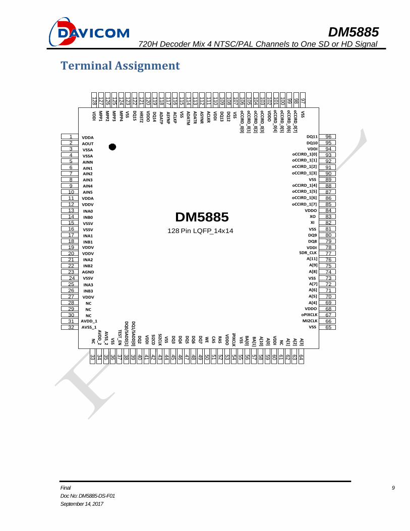
Terminal Assignment
DM5885128 Pin LQFP_14x14
1
2
3
4
5
6
7
8
9
10
11
12
13
14
15
16
17
18
19
20
21
22
23
24
25
26
27
28
29
30
31
32
96
95
94
93
92
91
90
89
88
87
86
85
84
83
82
81
80
79
78
77
76
75
74
73
72
71
70
69
68
67
66
65
97
98
99
100
101
102
103
104
105
106
107
108
109
110
111
112
113
114
115
116
117
118
119
120
121
122
123
124
125
126
127
128
VDDA
AOUT
VSSA
VSSA
AINN
AIN1AIN2
AIN3
AIN4
AIN5
VDDA
VDDV
INA0
INB0
VSSV
VSSV
INA1
INB1VDDV
VDDV
INA2
INB2
AGND
VSSV
INA3
INB3
VDDV
NC
NC
NCAVDD_1
AVSS_1
A[4]
VDDO
oPIXCLK
MI2CLK
VSS
DQ9
DQ8
VDDI
VSS
VDDO
XO
XI
VSS
DQ11
DQ10
VDDI
VSS
VD
DI
MPP1
MPP2
MPP3
MPP4
VSS
DQ
15
HR
STZ
VD
DO
VSS
AD
ATM
AD
ATR
ASYN
R
ACLK
R
VD
DI
DQ
13
DQ
12
VSS
VD
DO
VSS
A[5]
A[6]
A[7]
A[8]
A[9]
A[11]
SDR_CLK
oCCIRD_1[7]
oCCIRD_1[6]
oCCIRD_1[5]
oCCIRD_1[4]
oCCIRD_1[3]
oCCIRD_1[2]
oCCIRD_1[1]
oCCIRD_1[0]
oCCIRD
_0[4]
oCCIRD
_0[5]
oCCIRD
_0[6]
oCCIRD
_0[7]
oCCIRD
_0[0]
oCCIRD
_0[1]
oCCIRD
_0[2]
oCCIRD
_0[3]
DQ
14
AD
ATP
ASYN
P
ACLK
P
BA
[0]
BA
[1]
A[10]
A[0]
NC
A[1]
A[2]
A[3]
64
63
62
61
60
59
58
57
56
55
54
53
52
51
50
49
48
47
46
45
44
43
42
41
40
39
38
37
36
35
34
33
NC
AV
DD
_2
AV
SS_2
VSS
TEST_EN
DQ
0/SAD
D[1]
DQ
1/SAD
D[0]
DQ
2
VD
DI
SI2CD
SI2CLK
VSS
DQ
3
DQ
4
DQ
5
DQ
6
DQ
7
WE
CAS
RA
S
VD
DO
iPIXCLK
VD
DI
VSS
DM5885 720H Decoder Mix 4 NTSC/PAL Channels to One SD or HD Signal
Final 10
Doc No: DM5885-DS-F01
September 14, 2017
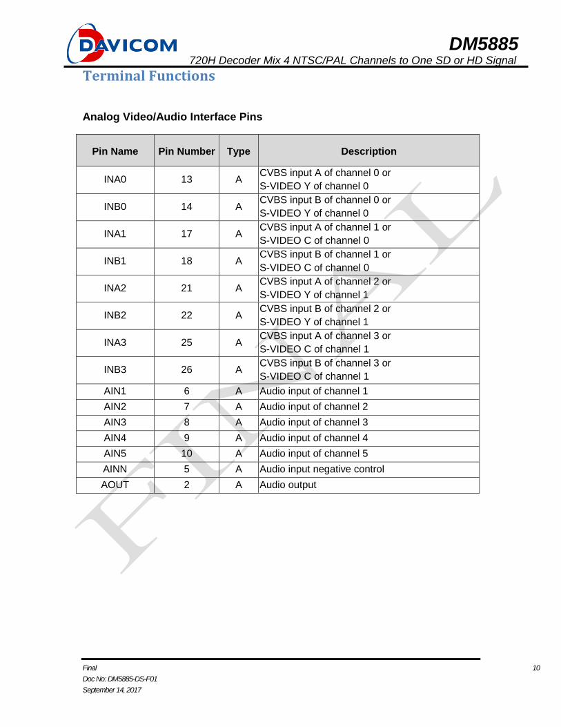
Terminal Functions
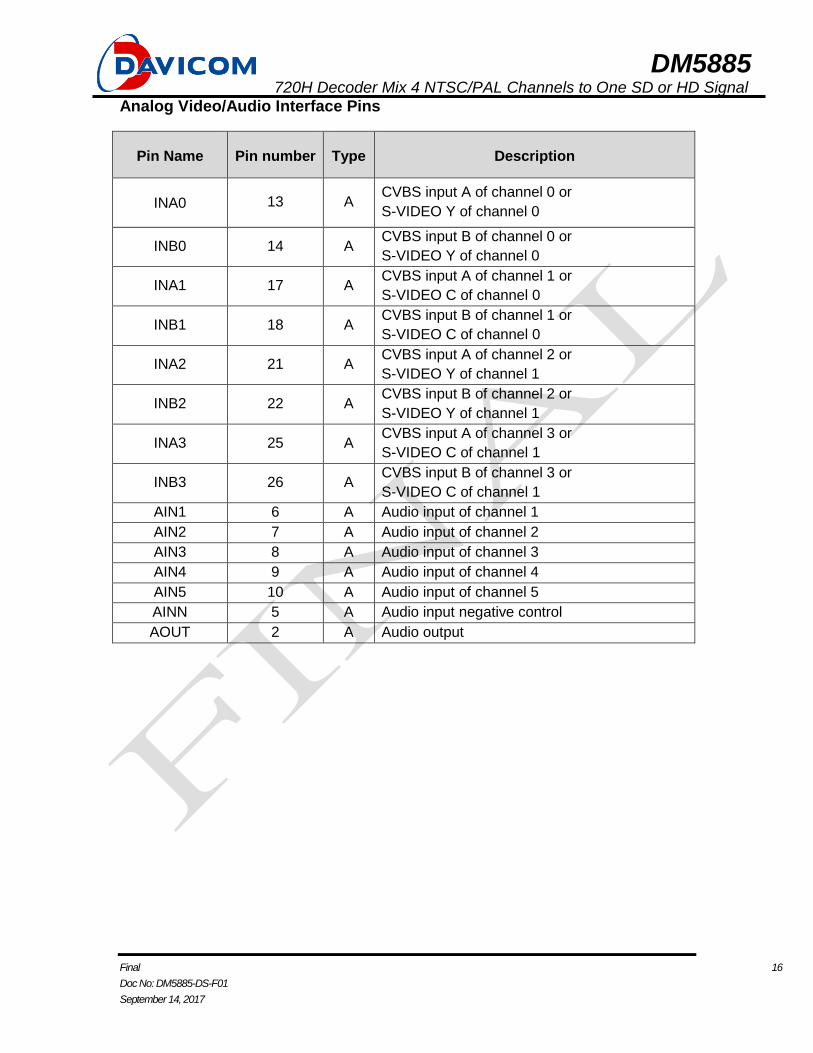
Analog Video/Audio Interface Pins
Pin Name Pin Number Type Description
INA0 13 A CVBS input A of channel 0 or
S-VIDEO Y of channel 0
INB0 14 A CVBS input B of channel 0 or
S-VIDEO Y of channel 0
INA1 17 A CVBS input A of channel 1 or
S-VIDEO C of channel 0
INB1 18 A CVBS input B of channel 1 or
S-VIDEO C of channel 0
INA2 21 A CVBS input A of channel 2 or
S-VIDEO Y of channel 1
INB2 22 A CVBS input B of channel 2 or
S-VIDEO Y of channel 1
INA3 25 A CVBS input A of channel 3 or
S-VIDEO C of channel 1
INB3 26 A CVBS input B of channel 3 or
S-VIDEO C of channel 1
AIN1 6 A Audio input of channel 1
AIN2 7 A Audio input of channel 2
AIN3 8 A Audio input of channel 3
AIN4 9 A Audio input of channel 4
AIN5 10 A Audio input of channel 5
AINN 5 A Audio input negative control
AOUT 2 A Audio output
DM5885 720H Decoder Mix 4 NTSC/PAL Channels to One SD or HD Signal
Final 11
Doc No: DM5885-DS-F01
September 14, 2017
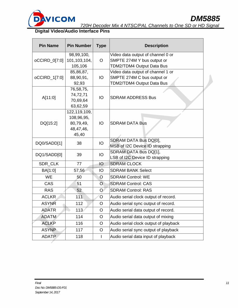
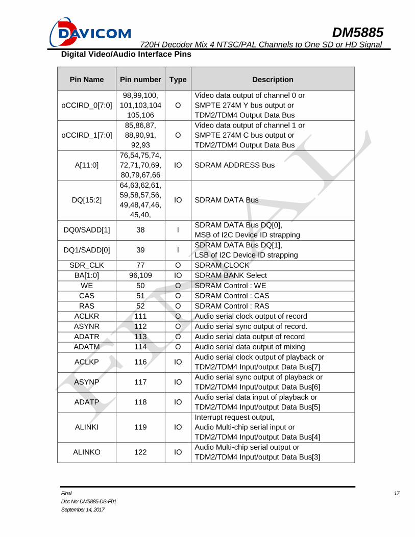
Digital Video/Audio Interface Pins
Pin Name Pin Number Type Description
oCCIRD_0[7:0]
98,99,100,
101,103,104,
105,106
O
Video data output of channel 0 or
SMPTE 274M Y bus output or
TDM2/TDM4 Output Data Bus
oCCIRD_1[7:0]
85,86,87,
88,90,91,
92,93
IO
Video data output of channel 1 or
SMPTE 274M C bus output or
TDM2/TDM4 Output Data Bus
A[11:0]
76,58,75,
74,72,71
70,69,64
63,62,59
IO SDRAM ADDRESS Bus
DQ[15:2]
122,119,109,
108,96,95,
80,79,49,
48,47,46,
45,40
IO SDRAM DATA Bus
DQ0/SADD[1] 38 IO SDRAM DATA Bus DQ[0],
MSB of I2C Device ID strapping
DQ1/SADD[0] 39 IO SDRAM DATA Bus DQ[1],
LSB of I2C Device ID strapping
SDR_CLK 77 IO SDRAM CLOCK
BA[1:0] 57,56 IO SDRAM BANK Select
WE 50 O SDRAM Control: WE
CAS 51 O SDRAM Control: CAS
RAS 52 O SDRAM Control: RAS
ACLKR 111 O Audio serial clock output of record.
ASYNR 112 O Audio serial sync output of record.
ADATR 113 O Audio serial data output of record.
ADATM 114 O Audio serial data output of mixing
ACLKP 116 O Audio serial clock output of playback
ASYNP 117 O Audio serial sync output of playback
ADATP 118 I Audio serial data input of playback
DM5885 720H Decoder Mix 4 NTSC/PAL Channels to One SD or HD Signal
Final 12
Doc No: DM5885-DS-F01
September 14, 2017
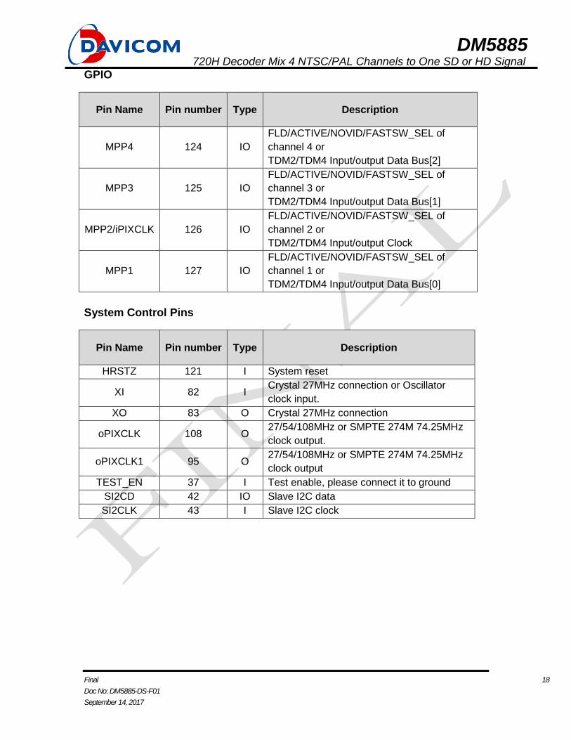
GPIO
Pin Name Pin Number Type Description
MPP4 124 IO FLD/ACTIVE/NOVID/FASTSW_SEL of channel
4
MPP3 125 IO FLD/ACTIVE/NOVID/FASTSW_SEL of channel
3
MPP2 126 IO FLD/ACTIVE/NOVID/FASTSW_SEL of channel
2
MPP1 127 IO FLD/ACTIVE/NOVID/FASTSW_SEL of channel
1
System Control Pins
Pin Name Pin Number Type Description
HRSTZ 121 I System reset.
XI 82 I Crystal 27 MHz connection or Oscillator clock
input.
XO 83 O For crystal 27 MHz connection.
oPIXCLK 67 O 27/54/108MHz or SMPTE 274M 74.25MHz clock
output
TEST_EN 37 I Test enable, please connect it to ground
SI2CD 42 IO Slave I2C data
SI2CLK 43 I Slave I2C clock
iPIXCLK 54 I CCIR656 27MHz or TMD 108 MHz clock input.
MI2CLK 66 IO Master i2c clock (open drain)
DM5885 720H Decoder Mix 4 NTSC/PAL Channels to One SD or HD Signal
Final 13
Doc No: DM5885-DS-F01
September 14, 2017
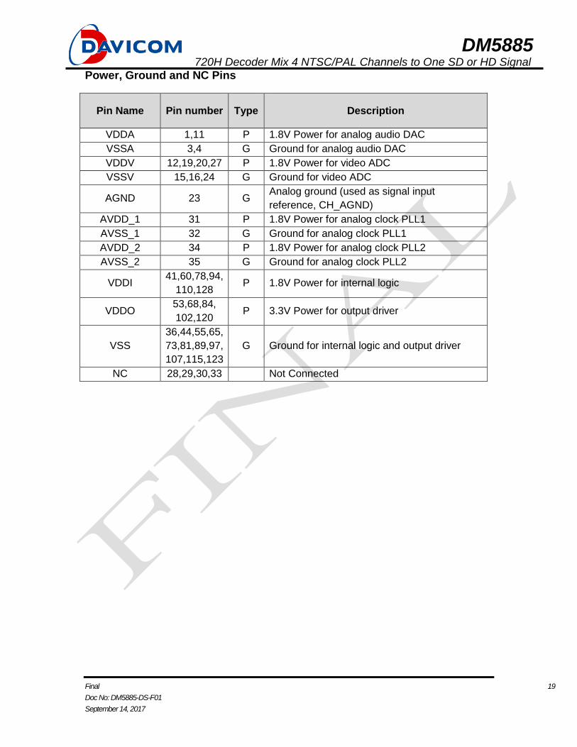
Power, Ground and NC Pins
Pin Name Pin Number Type Description
VDDA 1,11 P 1.8V Power for analog audio DAC
VSSA 3,4 G Ground for analog audio DAC
VDDV 12,19,20,27 P 1.8V Power for video ADC
VSSV 15,16,24 G Ground for video ADC
AGND 23 G Analog ground (used as signal input reference,
CH_AGND)
AVDD_1 31 P 1.8V Power for analog clock PLL1
AVSS_1 32 G Ground for analog clock PLL1
AVDD_2 34 P 1.8V Power for analog clock PLL2
AVSS_2 35 G Ground for analog clock PLL2
VDDI 41,60,78,94,
110,128 P 1.8V Power for internal logic.
VDDO 53,68,84,
102,120 P 3.3V Power for output driver
VSS
36,44,55,65,
73,81,89,97,
107,115,123
G Ground for internal logic and output driver
NC 28,29,30,33
61 Not Connected
DM5885 720H Decoder Mix 4 NTSC/PAL Channels to One SD or HD Signal
Final 14
Doc No: DM5885-DS-F01
September 14, 2017
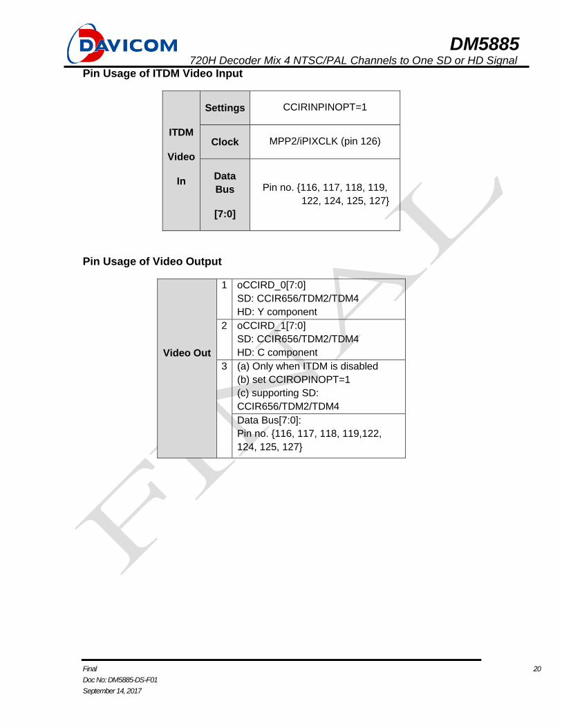
Pin Usage of ITDM Video Input
ITDM
Video
In
Settings CCIRINPINOPT=0
Clock iPIXCLK (pin 54)
Data Bus
[7:0]
oCCIRD_1[7:0]
Pin Usage of Video Output
Video Out
1 oCCIRD_0[7:0]
SD: CCIR656/TDM2/TDM4
HD: Y component
2 oCCIRD_1[7:0]
(Only when ITDM is disabled)
SD: CCIR656/TDM2/TDM4
HD: C component
DM5885 720H Decoder Mix 4 NTSC/PAL Channels to One SD or HD Signal
Final 15
Doc No: DM5885-DS-F01
September 14, 2017
Alternative assignment
(PINCFG = 2’h3 @ REG 6A)
DM5885128 Pin LQFP_14x14
1
2
3
4
5
6
7
8
9
10
11
12
13
14
15
16
17
18
19
20
21
22
23
24
25
26
27
28
29
30
31
32
96
95
94
93
92
91
90
89
88
87
86
85
84
83
82
81
80
79
78
77
76
75
74
73
72
71
70
69
68
67
66
65
97
98
99
10
0
10
1
10
2
10
3
10
4
10
5
10
6
10
7
10
8
10
9
11
0
11
1
11
2
11
3
11
4
11
5
11
6
11
7
11
8
11
9
12
0
12
1
12
2
12
3
12
4
12
5
12
6
12
7
12
8
VDDA
AOUT
VSSA
VSSA
AINN
AIN1AIN2
AIN3
AIN4
AIN5
VDDA
VDDV
INA0
INB0
VSSV
VSSV
INA1
INB1VDDV
VDDV
INA2
INB2
AGND
VSSV
INA3
INB3
VDDV
AVDD_1
NC
AVSS_1
NC
NC
A[4]
VDDO
A[1]
A[0]
VSS
A[3]
A[2]
VDDI
VSS
VDDO
XO
XI
VSS
BA[1]
oPIXCLK1
VDDI
VSS
VD
DI
MPP1
MPP2/iPIX
CLK
MPP3
MPP4
VSS
ALIN
KO
HR
STZ
VD
DO
VSS
AD
ATM
AD
ATR
ASYN
R
ACLK
R
VD
DI
BA
[0]
oPIXCLK
VSS
VD
DO
VSS
A[5]
A[6]
A[7]
A[8]
A[9]
A[11]
SDR_CLK
oCCIRD_1[7]
oCCIRD_1[6]
oCCIRD_1[5]
oCCIRD_1[4]
oCCIRD_1[3]
oCCIRD_1[2]
oCCIRD_1[1]
oCCIRD_1[0]
oCCIRD
_0[4]
oCCIRD
_0[5]
oCCIRD
_0[6]
oCCIRD
_0[7]
oCCIRD
_0[0]
oCCIRD
_0[1]
oCCIRD
_0[2]
oCCIRD
_0[3]
ALIN
KI
AD
ATP
ASYN
P
ACLK
P
DQ
8
DQ
9
DQ
10
DQ
11
DQ
12
DQ
13
DQ
14
DQ
1564
63
62
61
60
59
58
57
56
55
54
53
52
51
50
49
48
47
46
45
44
43
42
41
40
39
38
37
36
35
34
33
NC
AV
DD
_2
AV
SS_2
VSS
TEST_EN
DQ
0/SAD
D[1]
DQ
1/SAD
D[0]
DQ
2
VD
DI
SI2CD
SI2CLK
VSS
DQ
3
DQ
4
DQ
5
DQ
6
DQ
7
WE
CAS
RA
S
VD
DO
A[10]
VD
DI
VSS
(Alternative assignment)
Terminal functions of alternative assignment
(PINCFG = 2’h3 @ REG 6A)
DM5885 720H Decoder Mix 4 NTSC/PAL Channels to One SD or HD Signal
Final 16
Doc No: DM5885-DS-F01
September 14, 2017
Analog Video/Audio Interface Pins
Pin Name Pin number Type Description
INA0 13 A CVBS input A of channel 0 or
S-VIDEO Y of channel 0
INB0 14 A CVBS input B of channel 0 or
S-VIDEO Y of channel 0
INA1 17 A CVBS input A of channel 1 or
S-VIDEO C of channel 0
INB1 18 A CVBS input B of channel 1 or
S-VIDEO C of channel 0
INA2 21 A CVBS input A of channel 2 or
S-VIDEO Y of channel 1
INB2 22 A CVBS input B of channel 2 or
S-VIDEO Y of channel 1
INA3 25 A CVBS input A of channel 3 or
S-VIDEO C of channel 1
INB3 26 A CVBS input B of channel 3 or
S-VIDEO C of channel 1
AIN1 6 A Audio input of channel 1
AIN2 7 A Audio input of channel 2
AIN3 8 A Audio input of channel 3
AIN4 9 A Audio input of channel 4
AIN5 10 A Audio input of channel 5
AINN 5 A Audio input negative control
AOUT 2 A Audio output
DM5885 720H Decoder Mix 4 NTSC/PAL Channels to One SD or HD Signal
Final 17
Doc No: DM5885-DS-F01
September 14, 2017
Digital Video/Audio Interface Pins
Pin Name Pin number Type Description
oCCIRD_0[7:0]
98,99,100,
101,103,104
105,106
O
Video data output of channel 0 or
SMPTE 274M Y bus output or
TDM2/TDM4 Output Data Bus
oCCIRD_1[7:0]
85,86,87,
88,90,91,
92,93
O
Video data output of channel 1 or
SMPTE 274M C bus output or
TDM2/TDM4 Output Data Bus
A[11:0]
76,54,75,74,
72,71,70,69,
80,79,67,66
IO SDRAM ADDRESS Bus
DQ[15:2]
64,63,62,61,
59,58,57,56,
49,48,47,46,
45,40,
IO SDRAM DATA Bus
DQ0/SADD[1] 38 I SDRAM DATA Bus DQ[0],
MSB of I2C Device ID strapping
DQ1/SADD[0] 39 I SDRAM DATA Bus DQ[1],
LSB of I2C Device ID strapping
SDR_CLK 77 O SDRAM CLOCK
BA[1:0] 96,109 IO SDRAM BANK Select
WE 50 O SDRAM Control : WE
CAS 51 O SDRAM Control : CAS
RAS 52 O SDRAM Control : RAS
ACLKR 111 O Audio serial clock output of record
ASYNR 112 O Audio serial sync output of record.
ADATR 113 O Audio serial data output of record
ADATM 114 O Audio serial data output of mixing
ACLKP 116 IO Audio serial clock output of playback or
TDM2/TDM4 Input/output Data Bus[7]
ASYNP 117 IO Audio serial sync output of playback or
TDM2/TDM4 Input/output Data Bus[6]
ADATP 118 IO Audio serial data input of playback or
TDM2/TDM4 Input/output Data Bus[5]
ALINKI 119 IO
Interrupt request output,
Audio Multi-chip serial input or
TDM2/TDM4 Input/output Data Bus[4]
ALINKO 122 IO Audio Multi-chip serial output or
TDM2/TDM4 Input/output Data Bus[3]
DM5885 720H Decoder Mix 4 NTSC/PAL Channels to One SD or HD Signal
Final 18
Doc No: DM5885-DS-F01
September 14, 2017
GPIO
Pin Name Pin number Type Description
MPP4 124 IO
FLD/ACTIVE/NOVID/FASTSW_SEL of
channel 4 or
TDM2/TDM4 Input/output Data Bus[2]
MPP3 125 IO
FLD/ACTIVE/NOVID/FASTSW_SEL of
channel 3 or
TDM2/TDM4 Input/output Data Bus[1]
MPP2/iPIXCLK 126 IO
FLD/ACTIVE/NOVID/FASTSW_SEL of
channel 2 or
TDM2/TDM4 Input/output Clock
MPP1 127 IO
FLD/ACTIVE/NOVID/FASTSW_SEL of
channel 1 or
TDM2/TDM4 Input/output Data Bus[0]
System Control Pins
Pin Name Pin number Type Description
HRSTZ 121 I System reset
XI 82 I Crystal 27MHz connection or Oscillator
clock input.
XO 83 O Crystal 27MHz connection
oPIXCLK 108 O 27/54/108MHz or SMPTE 274M 74.25MHz
clock output.
oPIXCLK1 95 O 27/54/108MHz or SMPTE 274M 74.25MHz
clock output
TEST_EN 37 I Test enable, please connect it to ground
SI2CD 42 IO Slave I2C data
SI2CLK 43 I Slave I2C clock
DM5885 720H Decoder Mix 4 NTSC/PAL Channels to One SD or HD Signal
Final 19
Doc No: DM5885-DS-F01
September 14, 2017
Power, Ground and NC Pins
Pin Name Pin number Type Description
VDDA 1,11 P 1.8V Power for analog audio DAC
VSSA 3,4 G Ground for analog audio DAC
VDDV 12,19,20,27 P 1.8V Power for video ADC
VSSV 15,16,24 G Ground for video ADC
AGND 23 G Analog ground (used as signal input
reference, CH_AGND)
AVDD_1 31 P 1.8V Power for analog clock PLL1
AVSS_1 32 G Ground for analog clock PLL1
AVDD_2 34 P 1.8V Power for analog clock PLL2
AVSS_2 35 G Ground for analog clock PLL2
VDDI 41,60,78,94,
110,128 P 1.8V Power for internal logic
VDDO 53,68,84,
102,120 P 3.3V Power for output driver
VSS
36,44,55,65,
73,81,89,97,
107,115,123
G Ground for internal logic and output driver
NC 28,29,30,33 Not Connected
DM5885 720H Decoder Mix 4 NTSC/PAL Channels to One SD or HD Signal
Final 20
Doc No: DM5885-DS-F01
September 14, 2017
Pin Usage of ITDM Video Input
ITDM
Video
In
Settings CCIRINPINOPT=1
Clock MPP2/iPIXCLK (pin 126)
Data
Bus
[7:0]
Pin no. {116, 117, 118, 119,
122, 124, 125, 127}
Pin Usage of Video Output
Video Out
1 oCCIRD_0[7:0]
SD: CCIR656/TDM2/TDM4
HD: Y component
2 oCCIRD_1[7:0]
SD: CCIR656/TDM2/TDM4
HD: C component
3 (a) Only when ITDM is disabled
(b) set CCIROPINOPT=1
(c) supporting SD:
CCIR656/TDM2/TDM4
Data Bus[7:0]:
Pin no. {116, 117, 118, 119,122,
124, 125, 127}
DM5885 720H Decoder Mix 4 NTSC/PAL Channels to One SD or HD Signal
Final 21
Doc No: DM5885-DS-F01
September 14, 2017
Block Diagram
M
U
X
M
U
X
ADC
Video Decoder
VIN1A
VIN1B
16/32 bit SDRAM IF
1xHD / 2xSD Mixer
5x Audio ADC
Audio DAC
I2S IF
Audio cas
IF
Audio
Mix
OTDM
IFM
U
X
M
U
X
VIN3A
VIN3B
ACLKR/ASYNR/
ADATRADATM
ADATPACLKP/ASYNP
VD0[7:0] / HD_Y
VD1[7:0] / HD_C
VD2[7:0]
VD3[7:0]
MIX_TDMO/
MIX_TDMI
ALINKO
ALINKIAOUT
AIN5
AIN4
AIN3
AIN2
AIN1
VIN4B
VIN4A
VIN2B
VIN2A
ADC
Video Decoder
Video Decoder
Video Decoder
DM5885 720H Decoder Mix 4 NTSC/PAL Channels to One SD or HD Signal
Final 22
Doc No: DM5885-DS-F01
September 14, 2017
Video Decoder
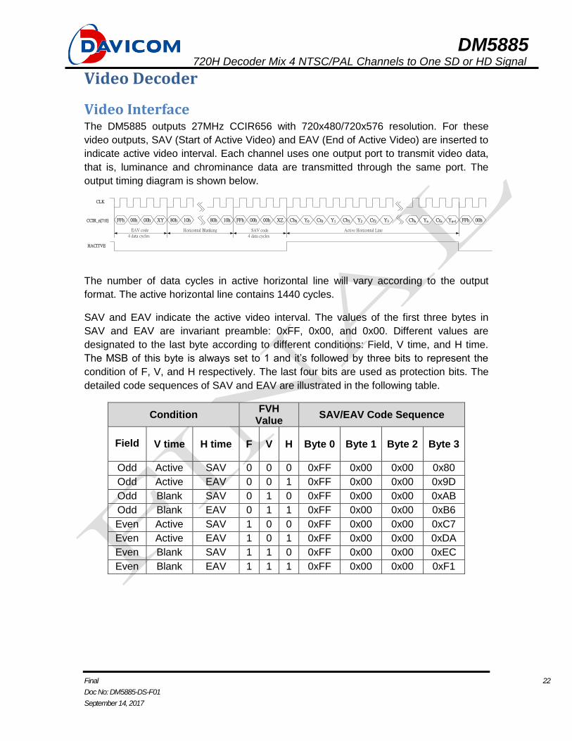
Video Interface The DM5885 outputs 27MHz CCIR656 with 720x480/720x576 resolution. For these
video outputs, SAV (Start of Active Video) and EAV (End of Active Video) are inserted to
indicate active video interval. Each channel uses one output port to transmit video data,
that is, luminance and chrominance data are transmitted through the same port. The
output timing diagram is shown below.
FFh 00h 00h XY 80h 10h 80h 10h FFh 00h 00h XZ Cb0 Y0 Cr0 Y1 Cb2 Y2 Cr2 Y3 Cbn Yn Crn Yn+1 FFh 00h
EAV code
4 data cycles
Horizontal Blanking SAV code
4 data cycles
Active Horizontal Line
CLK
CCIR_n[7:0]
HACITVE
The number of data cycles in active horizontal line will vary according to the output
format. The active horizontal line contains 1440 cycles.
SAV and EAV indicate the active video interval. The values of the first three bytes in
SAV and EAV are invariant preamble: 0xFF, 0x00, and 0x00. Different values are
designated to the last byte according to different conditions: Field, V time, and H time.
The MSB of this byte is always set to 1 and it’s followed by three bits to represent the
condition of F, V, and H respectively. The last four bits are used as protection bits. The
detailed code sequences of SAV and EAV are illustrated in the following table.
Condition FVH
Value SAV/EAV Code Sequence
Field V time H time F V H Byte 0 Byte 1 Byte 2 Byte 3
Odd Active SAV 0 0 0 0xFF 0x00 0x00 0x80
Odd Active EAV 0 0 1 0xFF 0x00 0x00 0x9D
Odd Blank SAV 0 1 0 0xFF 0x00 0x00 0xAB
Odd Blank EAV 0 1 1 0xFF 0x00 0x00 0xB6
Even Active SAV 1 0 0 0xFF 0x00 0x00 0xC7
Even Active EAV 1 0 1 0xFF 0x00 0x00 0xDA
Even Blank SAV 1 1 0 0xFF 0x00 0x00 0xEC
Even Blank EAV 1 1 1 0xFF 0x00 0x00 0xF1
DM5885 720H Decoder Mix 4 NTSC/PAL Channels to One SD or HD Signal
Final 23
Doc No: DM5885-DS-F01
September 14, 2017
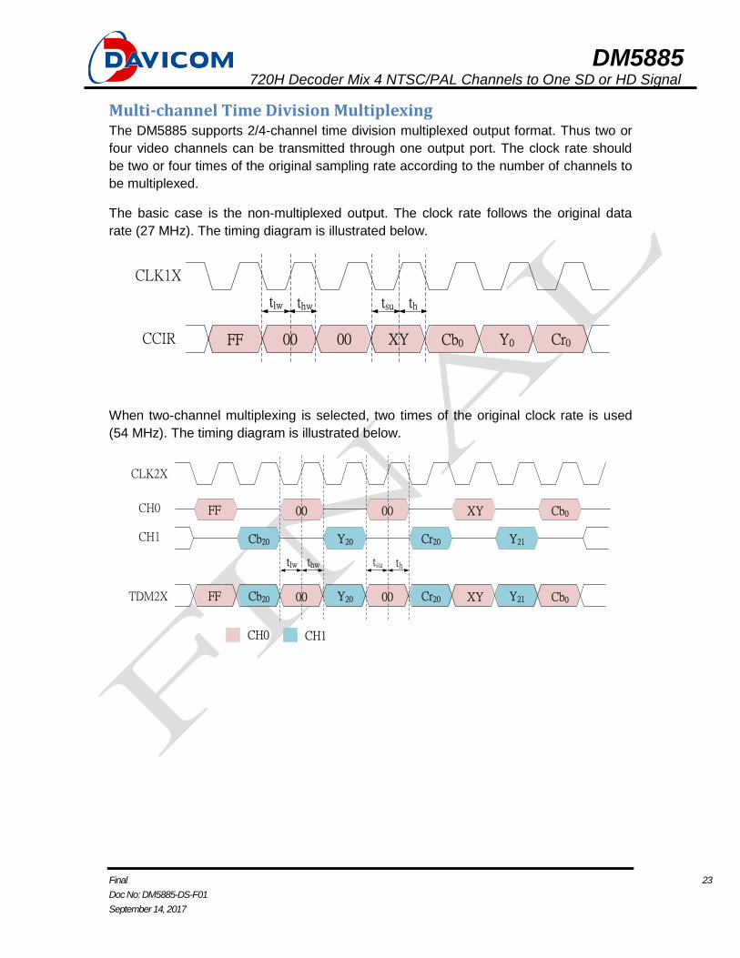
Multi-channel Time Division Multiplexing The DM5885 supports 2/4-channel time division multiplexed output format. Thus two or
four video channels can be transmitted through one output port. The clock rate should
be two or four times of the original sampling rate according to the number of channels to
be multiplexed.
The basic case is the non-multiplexed output. The clock rate follows the original data
rate (27 MHz). The timing diagram is illustrated below.
FF 00 00 XY Cb0 Y0 Cr0
tlw thw tsu th
CLK1X
CCIR
When two-channel multiplexing is selected, two times of the original clock rate is used
(54 MHz). The timing diagram is illustrated below.
FF 00 00 XY Cb0
FF 00 00 XY Cb0
Cb20 Y20 Cr20 Y21
Cb20 Y20 Cr20 Y21
tlw thw tsu th
CH0 CH1
CLK2X
CH0
CH1
TDM2X
DM5885 720H Decoder Mix 4 NTSC/PAL Channels to One SD or HD Signal
Final 24
Doc No: DM5885-DS-F01
September 14, 2017
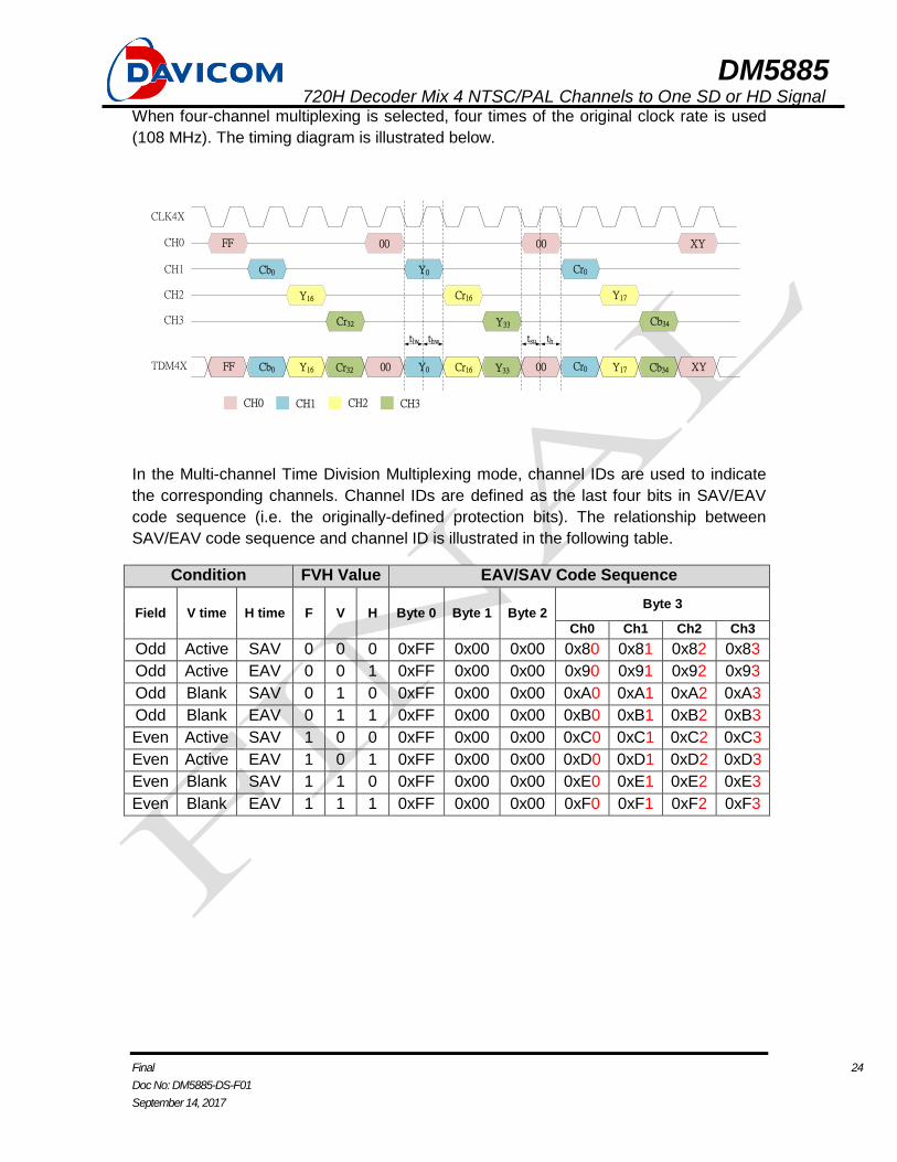
When four-channel multiplexing is selected, four times of the original clock rate is used
(108 MHz). The timing diagram is illustrated below.
tlw thw tsu th
CH0 CH1
FF 00 00 XY
FF 00 00 XY
Cb0 Y0 Cr0
Y16 Cr16 Y17
Cr32 Y33 Cb34
Cb0 Y0 Cr0Y16 Cr16 Y17Cr32 Y33 Cb34
CH2 CH3
CLK4X
CH0
CH1
CH2
CH3
TDM4X
In the Multi-channel Time Division Multiplexing mode, channel IDs are used to indicate
the corresponding channels. Channel IDs are defined as the last four bits in SAV/EAV
code sequence (i.e. the originally-defined protection bits). The relationship between
SAV/EAV code sequence and channel ID is illustrated in the following table.
Condition FVH Value EAV/SAV Code Sequence
Field V time H time F V H Byte 0 Byte 1 Byte 2 Byte 3
Ch0 Ch1 Ch2 Ch3
Odd Active SAV 0 0 0 0xFF 0x00 0x00 0x80 0x81 0x82 0x83
Odd Active EAV 0 0 1 0xFF 0x00 0x00 0x90 0x91 0x92 0x93
Odd Blank SAV 0 1 0 0xFF 0x00 0x00 0xA0 0xA1 0xA2 0xA3
Odd Blank EAV 0 1 1 0xFF 0x00 0x00 0xB0 0xB1 0xB2 0xB3
Even Active SAV 1 0 0 0xFF 0x00 0x00 0xC0 0xC1 0xC2 0xC3
Even Active EAV 1 0 1 0xFF 0x00 0x00 0xD0 0xD1 0xD2 0xD3
Even Blank SAV 1 1 0 0xFF 0x00 0x00 0xE0 0xE1 0xE2 0xE3
Even Blank EAV 1 1 1 0xFF 0x00 0x00 0xF0 0xF1 0xF2 0xF3
DM5885 720H Decoder Mix 4 NTSC/PAL Channels to One SD or HD Signal
Final 25
Doc No: DM5885-DS-F01
September 14, 2017
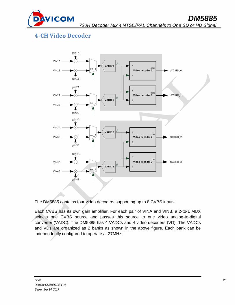
4-CH Video Decoder
sel_1
sel_2
VIN1A
VIN1B
VIN2A
VIN2B
gain2A
gain2B
gain1A
gain1B
VADC 0
VADC 1
Video decoder 0
A
B
CCIR
oCCIRD_0
Video decoder 1
A
B
CCIR
oCCIRD_1
sel_3
sel_4
VIN3A
VIN3B
VIN4A
VIN4B
gain4A
gain4B
gain3A
gain3B
VADC 2
VADC 3
Video decoder 2
A
B
CCIR
oCCIRD_2
Video decoder 3
A
B
CCIR
oCCIRD_3
A
A
B
B
The DM5885 contains four video decoders supporting up to 8 CVBS inputs.
Each CVBS has its own gain amplifier. For each pair of VINA and VINB, a 2-to-1 MUX
selects one CVBS source and passes this source to one video analog-to-digital
converter (VADC). The DM5885 has 4 VADCs and 4 video decoders (VD). The VADCs
and VDs are organized as 2 banks as shown in the above figure. Each bank can be
independently configured to operate at 27MHz.
DM5885 720H Decoder Mix 4 NTSC/PAL Channels to One SD or HD Signal
Final 26
Doc No: DM5885-DS-F01
September 14, 2017
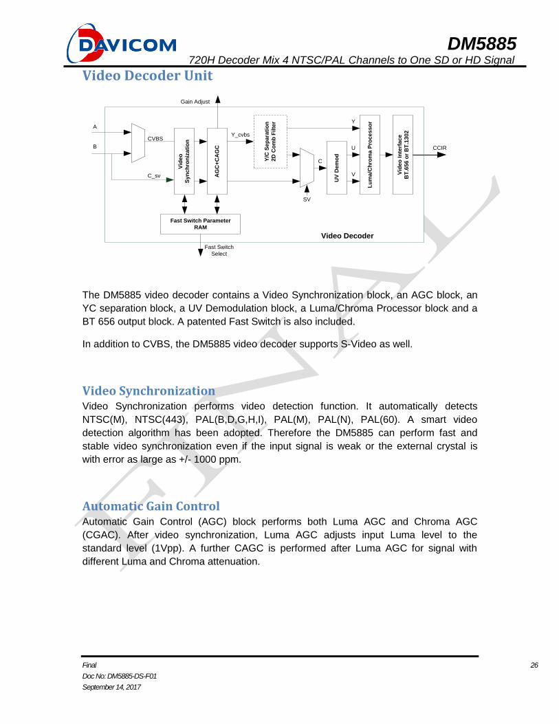
Video Decoder Unit
Vid
eo
Sy
nc
hro
niz
ati
on
Y/C
Se
pa
rati
on
2D
Co
mb
Filte
r
A
B
Y_cvbs
C_sv
SV
Y
C
UV
De
mo
d
Lu
ma/C
hro
ma
Pro
ce
ss
or
U
V Vid
eo
In
terf
ac
e
BT
.65
6 o
r B
T.1
30
2
Video Decoder
CCIR
Fast Switch Parameter
RAM
Fast Switch
Select
AG
C+
CA
GC
Gain Adjust
CVBS
The DM5885 video decoder contains a Video Synchronization block, an AGC block, an
YC separation block, a UV Demodulation block, a Luma/Chroma Processor block and a
BT 656 output block. A patented Fast Switch is also included.
In addition to CVBS, the DM5885 video decoder supports S-Video as well.
Video Synchronization Video Synchronization performs video detection function. It automatically detects
NTSC(M), NTSC(443), PAL(B,D,G,H,I), PAL(M), PAL(N), PAL(60). A smart video
detection algorithm has been adopted. Therefore the DM5885 can perform fast and
stable video synchronization even if the input signal is weak or the external crystal is
with error as large as +/- 1000 ppm.
Automatic Gain Control Automatic Gain Control (AGC) block performs both Luma AGC and Chroma AGC
(CGAC). After video synchronization, Luma AGC adjusts input Luma level to the
standard level (1Vpp). A further CAGC is performed after Luma AGC for signal with
different Luma and Chroma attenuation.

DM5885 720H Decoder Mix 4 NTSC/PAL Channels to One SD or HD Signal
Final 27
Doc No: DM5885-DS-F01
September 14, 2017
Y/C Separation Y/C Separation is for CVBS input only. After this block CVBS signal is separated into
Luma and Chroma components. A 5-H 2D comb filter is adapted in the Y/C separation
block.
UV demodulation After Y/C separation, the UV demodulation block performs UV demodulation to the
Chroma component. The phase and frequency of the UV demodulation is from a color
burst subcarrier tracking block for both NTSC and PAL mode. A UV demodulation LPF is
also adopted to filter out chroma noise.
Luma/Chroma Processor This block contains a programmable Luma sharpness filter. Hue, Saturation, Brightness
and Contrast adjustment are also supported. The adjusted video is then transformed
from YUV to YCbCr domain for CCIR656 output interface.
Video Interface The DM5885 video decoder supports 27MHz BT.656 video output format. A horizontal
cropping function also included in this block.
Fast Switch Parameter RAM The DM5885 features a patented hardware video source fast switch function. The Fast
Switch block has a table which stores video characteristic. Each time HW switches to a
previously tracked video source it could complete video synchronization within several
lines. With this feature, the DM5885 can decode up to 8 CVBS with little frame rate loss.
DM5885 720H Decoder Mix 4 NTSC/PAL Channels to One SD or HD Signal
Final 28
Doc No: DM5885-DS-F01
September 14, 2017
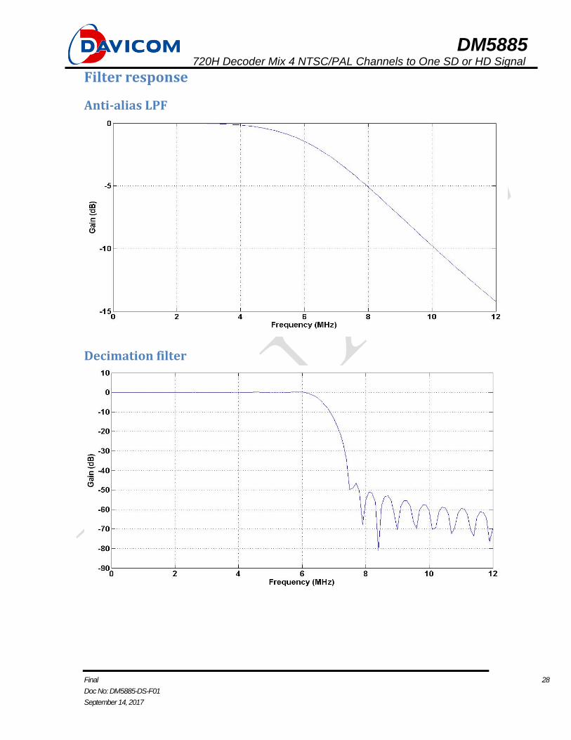
Filter response
Anti-alias LPF
Decimation filter
DM5885 720H Decoder Mix 4 NTSC/PAL Channels to One SD or HD Signal
Final 29
Doc No: DM5885-DS-F01
September 14, 2017
Luma notch filter
Chroma band pass filter
DM5885 720H Decoder Mix 4 NTSC/PAL Channels to One SD or HD Signal
Final 30
Doc No: DM5885-DS-F01
September 14, 2017
Y sharpness filter
NTSC
PAL
DM5885 720H Decoder Mix 4 NTSC/PAL Channels to One SD or HD Signal
Final 31
Doc No: DM5885-DS-F01
September 14, 2017
UV demodulation low pass filter
DM5885 720H Decoder Mix 4 NTSC/PAL Channels to One SD or HD Signal
Final 32
Doc No: DM5885-DS-F01
September 14, 2017
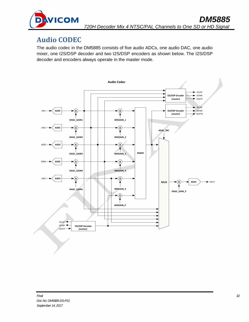
Audio CODEC The audio codec in the DM5885 consists of five audio ADCs, one audio DAC, one audio
mixer, one I2S/DSP decoder and two I2S/DSP encoders as shown below. The I2S/DSP
decoder and encoders always operate in the master mode.
AIN1 X
X
X
X
X
DAGC_GAIN1
DAGC_GAIN2
DAGC_GAIN3
DAGC_GAIN4
DAGC_GAIN5
I2S/DSP Encoder
MIXER
ACLKR
ASYNR
ADATR
ADATM
I2S/DSP Decoder
ACLKP
ASYNP
ADATP
X
DAGC_GAIN_P
AOUT
AADC
AIN2
AIN3
AIN4
AIN5
MUX ADAC
Audio Codec
X
X
X
X
X
MIXGAIN_1
MIXGAIN_2
MIXGAIN_3
MIXGAIN_4
MIXGAIN_5
X
MIXGAIN_P
AADC
AADC
AADC
AADC
ADAC_SRC
I2S/DSP Encoder
ACLKR
ASYNR
(master)
(master)
(master)
DM5885 720H Decoder Mix 4 NTSC/PAL Channels to One SD or HD Signal
Final 33
Doc No: DM5885-DS-F01
September 14, 2017
The I2S/DSP decoder is used for playback of digital input. It generates ACLKP and
ASYNP signals and accepts serial data via ADATP from a slave device. The levels of
the five analog audio inputs (AIN1 ~ AIN5) are programmable via the registers
DAGC_GAIN1, DAGC_GAIN2, DAGC_GAIN3, DAGC_GAIN4 and DAGC_GAIN5. The
six input audio sources can be mixed by the used-defined ratio specified by registers
MIXGAIN_1, MIXGAIN_2, MIXGAIN_3, MIXGAIN_4, MIXGAIN_5, MIXGAIN_P. The
mixed audio can be output through I2S/DSP encoder or DAC.
The codec provides three interfaces for audio output. The audio DAC can output analog
audio for any one of the six input audio sources or the mixed audio. The analog output
level is adjustable via register DAGC_GAIN_P. Two I2S/DSP encoders are present to
output digital audio signal. The first one generates ACLKR, ASYNR and ADATR to
output the 4 recorded audio inputs. The second encoder uses ADATM and shares the
other two signals (ACLKR and ASYNR) to output the mixed audio.
DM5885 720H Decoder Mix 4 NTSC/PAL Channels to One SD or HD Signal
Final 34
Doc No: DM5885-DS-F01
September 14, 2017
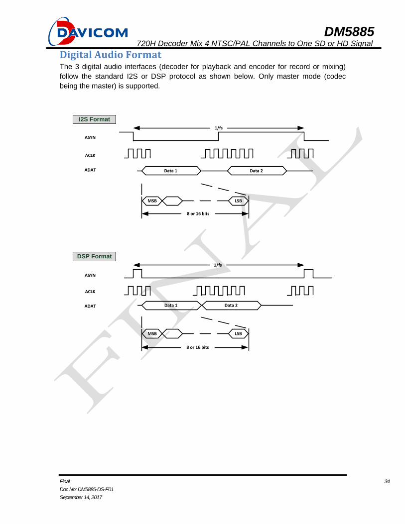
Digital Audio Format The 3 digital audio interfaces (decoder for playback and encoder for record or mixing)
follow the standard I2S or DSP protocol as shown below. Only master mode (codec
being the master) is supported.
ASYN
ACLK
ADAT Data 1
MSB LSB
8 or 16 bits
I2S Format
ASYN
ACLK
ADAT
MSB LSB
DSP Format
Data 2
Data 1 Data 2
8 or 16 bits
1/fs
1/fs
DM5885 720H Decoder Mix 4 NTSC/PAL Channels to One SD or HD Signal
Final 35
Doc No: DM5885-DS-F01
September 14, 2017
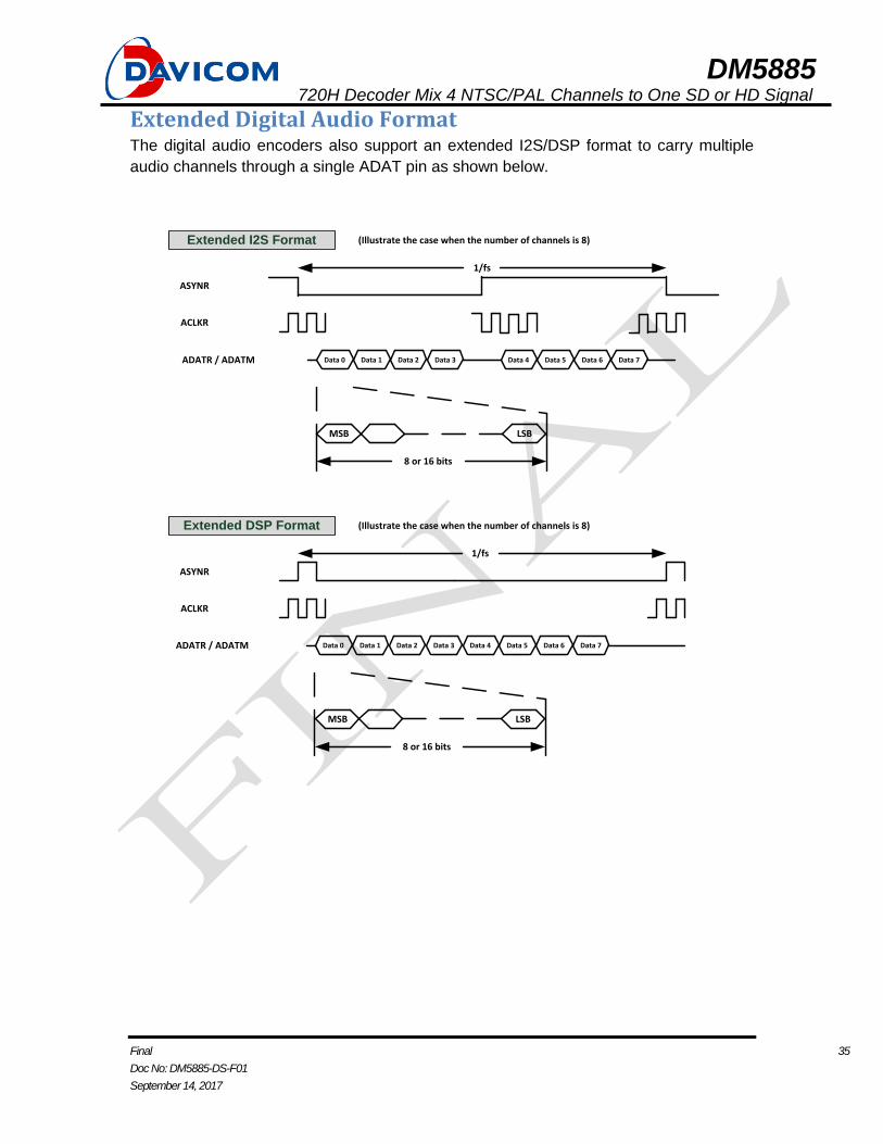
Extended Digital Audio Format The digital audio encoders also support an extended I2S/DSP format to carry multiple
audio channels through a single ADAT pin as shown below.
ASYNR
ACLKR
ADATR / ADATM Data 0
MSB LSB
Extended I2S Format
ASYNR
ACLKR
Extended DSP Format
Data 1 Data 2 Data 3 Data 4 Data 5 Data 6 Data 7
ADATR / ADATM Data 0
MSB LSB
8 or 16 bits
Data 1 Data 2 Data 3 Data 4 Data 5 Data 6 Data 7
8 or 16 bits
(Illustrate the case when the number of channels is 8)
1/fs
1/fs
(Illustrate the case when the number of channels is 8)
DM5885 720H Decoder Mix 4 NTSC/PAL Channels to One SD or HD Signal
Final 36
Doc No: DM5885-DS-F01
September 14, 2017
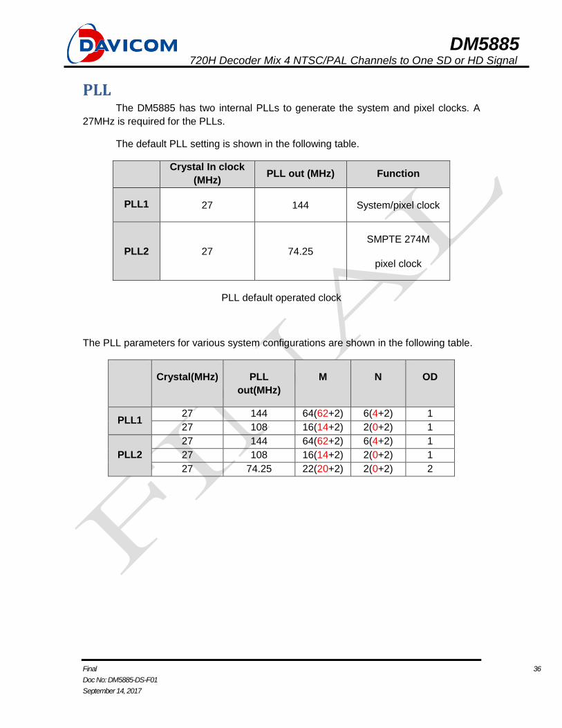
PLL The DM5885 has two internal PLLs to generate the system and pixel clocks. A
27MHz is required for the PLLs.
The default PLL setting is shown in the following table.
Crystal In clock
(MHz) PLL out (MHz) Function
PLL1 27 144 System/pixel clock
PLL2 27 74.25
SMPTE 274M
pixel clock
PLL default operated clock
The PLL parameters for various system configurations are shown in the following table.
Crystal(MHz) PLL
out(MHz)
M N OD
PLL1 27 144 64(62+2) 6(4+2) 1
27 108 16(14+2) 2(0+2) 1
PLL2
27 144 64(62+2) 6(4+2) 1
27 108 16(14+2) 2(0+2) 1
27 74.25 22(20+2) 2(0+2) 2
DM5885 720H Decoder Mix 4 NTSC/PAL Channels to One SD or HD Signal
Final 37
Doc No: DM5885-DS-F01
September 14, 2017
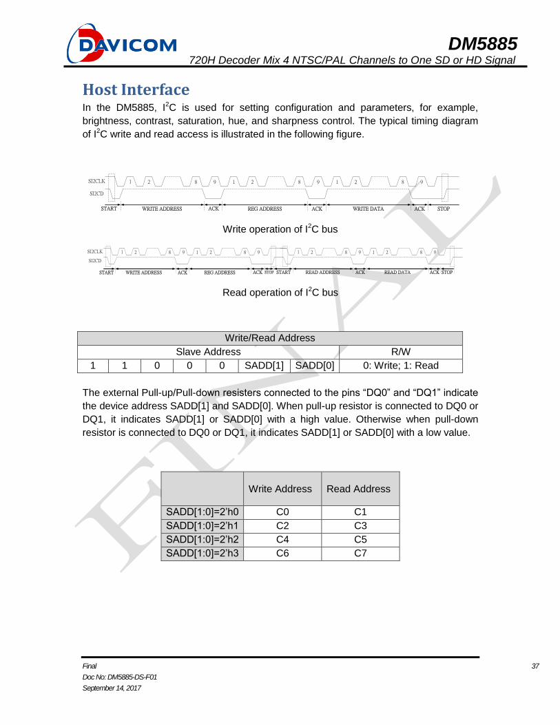
Host Interface In the DM5885, I2C is used for setting configuration and parameters, for example,
brightness, contrast, saturation, hue, and sharpness control. The typical timing diagram
of I2C write and read access is illustrated in the following figure.
SI2CLK
SI2CD
1 2 8 9 1 2 8 9 1 2 8 9
START WRITE ADDRESS ACK REG ADDRESS ACK WRITE DATA ACK STOP
Write operation of I2C bus
SI2CLK
SI2CD
1 2 8 9 1 2 8 9
START WRITE ADDRESS ACK REG ADDRESS ACK STOP
1 2 8 9 1 2 8 9
READ ADDRESS ACK READ DATA ACK STOPSTART
Read operation of I2C bus
Write/Read Address
Slave Address R/W
1 1 0 0 0 SADD[1] SADD[0] 0: Write; 1: Read
The external Pull-up/Pull-down resisters connected to the pins “DQ0” and “DQ1” indicate
the device address SADD[1] and SADD[0]. When pull-up resistor is connected to DQ0 or
DQ1, it indicates SADD[1] or SADD[0] with a high value. Otherwise when pull-down
resistor is connected to DQ0 or DQ1, it indicates SADD[1] or SADD[0] with a low value.
Write Address Read Address
SADD[1:0]=2’h0 C0 C1
SADD[1:0]=2’h1 C2 C3
SADD[1:0]=2’h2 C4 C5
SADD[1:0]=2’h3 C6 C7
DM5885 720H Decoder Mix 4 NTSC/PAL Channels to One SD or HD Signal
Final 38
Doc No: DM5885-DS-F01
September 14, 2017
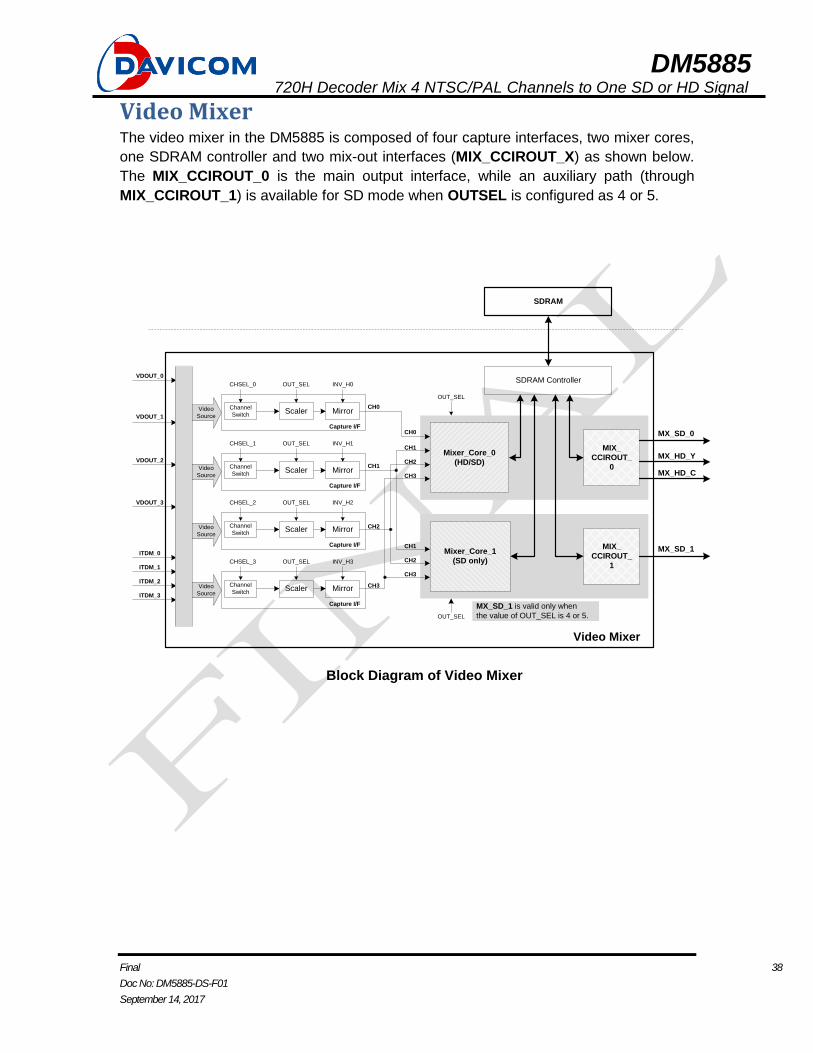
Video Mixer The video mixer in the DM5885 is composed of four capture interfaces, two mixer cores,
one SDRAM controller and two mix-out interfaces (MIX_CCIROUT_X) as shown below.
The MIX_CCIROUT_0 is the main output interface, while an auxiliary path (through
MIX_CCIROUT_1) is available for SD mode when OUTSEL is configured as 4 or 5.
SDRAM
SDRAM Controller
MIX_
CCIROUT_
0
ITDM_0
Video Mixer
VDOUT_0
VDOUT_1
VDOUT_2
VDOUT_3
Block Diagram of Video Mixer
INV_H0
CH0Scaler Mirror
Channel
Switch
Capture I/F
Video
Source
OUT_SELCHSEL_0
INV_H1
CH1Scaler Mirror
Channel
Switch
Capture I/F
Video
Source
OUT_SELCHSEL_1
INV_H2
CH2Scaler MirrorChannel
Switch
Capture I/F
Video
Source
OUT_SELCHSEL_2
INV_H3
CH3Scaler MirrorChannel
Switch
Capture I/F
Video
Source
OUT_SELCHSEL_3ITDM_1
ITDM_2
ITDM_3
Mixer_Core_0
(HD/SD)
Mixer_Core_1
(SD only)
CH0
CH1
CH1
CH2
CH2
CH3
CH3
MIX_
CCIROUT_
1
MX_SD_0
MX_HD_Y
MX_HD_C
MX_SD_1
MX_SD_1 is valid only when
the value of OUT_SEL is 4 or 5.
OUT_SEL
OUT_SEL
DM5885 720H Decoder Mix 4 NTSC/PAL Channels to One SD or HD Signal
Final 39
Doc No: DM5885-DS-F01
September 14, 2017
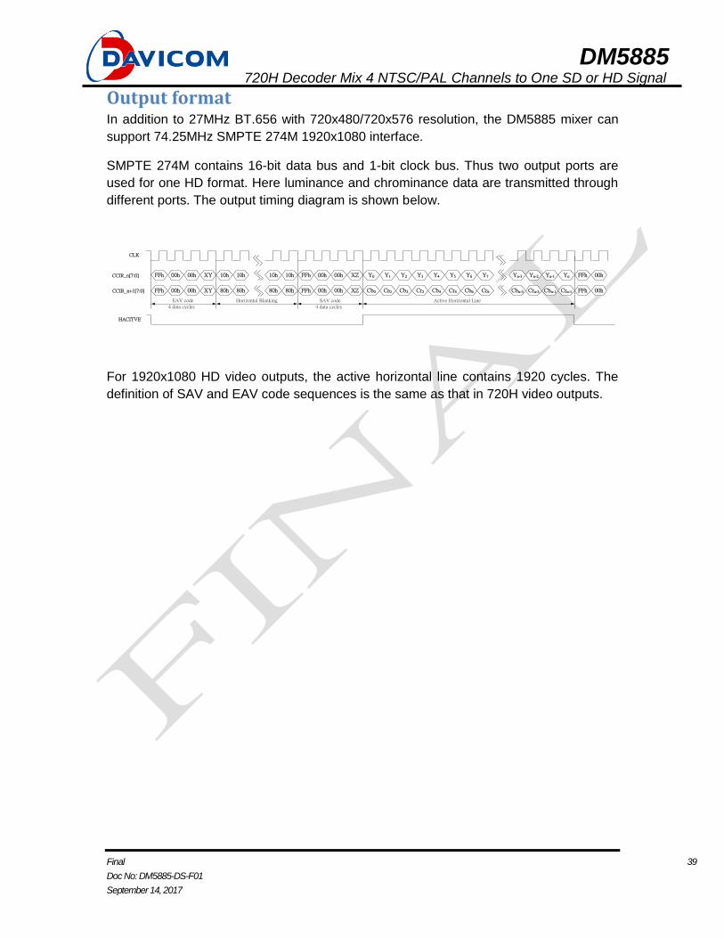
Output format In addition to 27MHz BT.656 with 720x480/720x576 resolution, the DM5885 mixer can
support 74.25MHz SMPTE 274M 1920x1080 interface.
SMPTE 274M contains 16-bit data bus and 1-bit clock bus. Thus two output ports are
used for one HD format. Here luminance and chrominance data are transmitted through
different ports. The output timing diagram is shown below.
FFh 00h 00h XY 10h 10h 10h 10h FFh 00h 00h XZ Y0 Y1 Y2 Y3 Y4 Y5 Y6 Y7 Yn-3 Yn-2 Yn-1 Yn FFh 00h
EAV code
4 data cycles
Horizontal Blanking SAV code
4 data cycles
Active Horizontal Line
CLK
CCIR_n[7:0]
HACITVE
FFh 00h 00h XY 80h 80h 80h 80h FFh 00h 00h XZ Cb0 Cr0 Cb2 Cr2 Cb4 Cr4 Cb6 Cr6 Cbn-3 Crn-3 Cbn-1 Crn-1 FFh 00hCCIR_n+1[7:0]
For 1920x1080 HD video outputs, the active horizontal line contains 1920 cycles. The
definition of SAV and EAV code sequences is the same as that in 720H video outputs.
DM5885 720H Decoder Mix 4 NTSC/PAL Channels to One SD or HD Signal
Final 40
Doc No: DM5885-DS-F01
September 14, 2017
Video Mixer Block
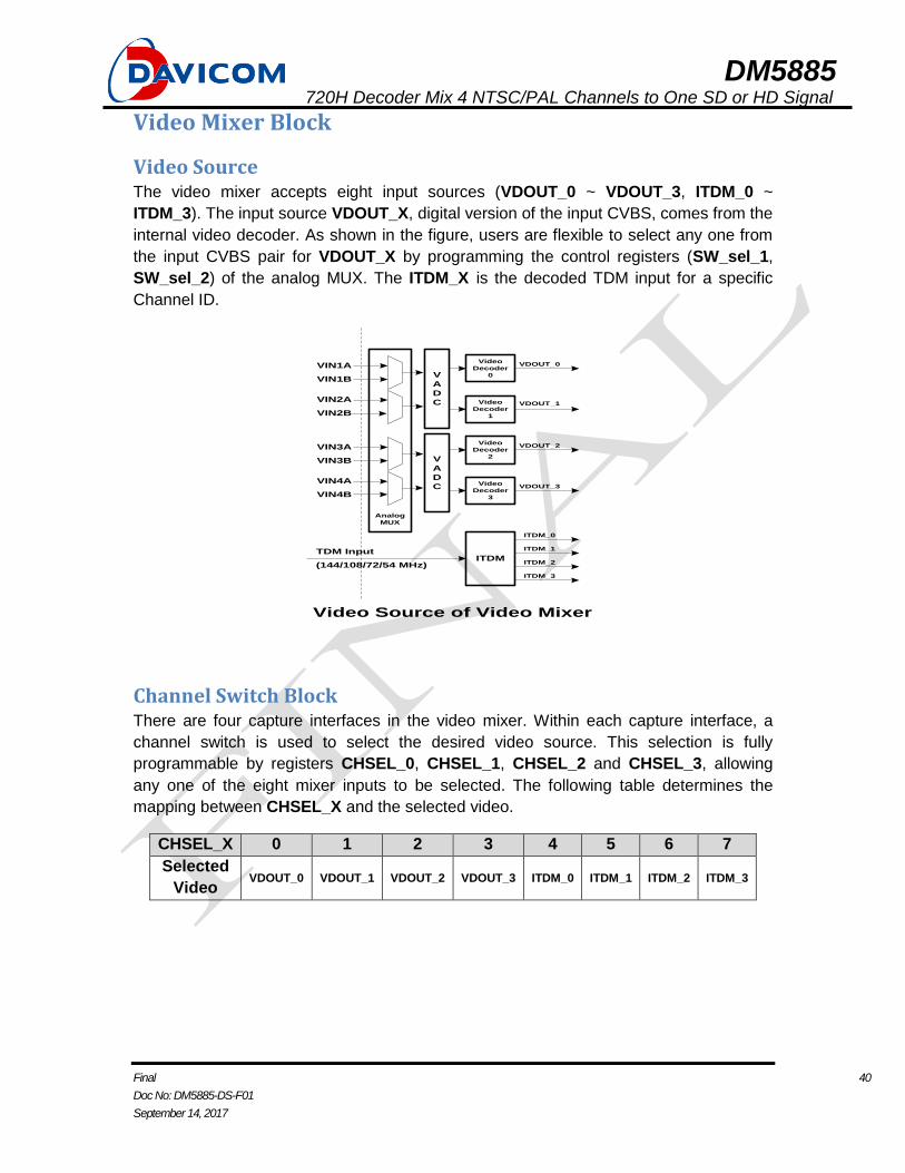
Video Source The video mixer accepts eight input sources (VDOUT_0 ~ VDOUT_3, ITDM_0 ~
ITDM_3). The input source VDOUT_X, digital version of the input CVBS, comes from the
internal video decoder. As shown in the figure, users are flexible to select any one from
the input CVBS pair for VDOUT_X by programming the control registers (SW_sel_1,
SW_sel_2) of the analog MUX. The ITDM_X is the decoded TDM input for a specific
Channel ID.
Video
Decoder
0
Video
Decoder
1
Video
Decoder
2
Video
Decoder
3
ITDMTDM Input
ITDM_0
VDOUT_0
VDOUT_1
VDOUT_2
VDOUT_3
V
A
D
C
V
A
D
C
VIN1A
VIN1B
VIN2A
VIN2B
VIN3A
VIN3B
VIN4A
VIN4B
Analog
MUX
ITDM_1
ITDM_2
ITDM_3
(144/108/72/54 MHz)
Video Source of Video Mixer
Channel Switch Block There are four capture interfaces in the video mixer. Within each capture interface, a
channel switch is used to select the desired video source. This selection is fully
programmable by registers CHSEL_0, CHSEL_1, CHSEL_2 and CHSEL_3, allowing
any one of the eight mixer inputs to be selected. The following table determines the
mapping between CHSEL_X and the selected video.
CHSEL_X 0 1 2 3 4 5 6 7
Selected
Video VDOUT_0 VDOUT_1 VDOUT_2 VDOUT_3 ITDM_0 ITDM_1 ITDM_2 ITDM_3
DM5885 720H Decoder Mix 4 NTSC/PAL Channels to One SD or HD Signal
Final 41
Doc No: DM5885-DS-F01
September 14, 2017
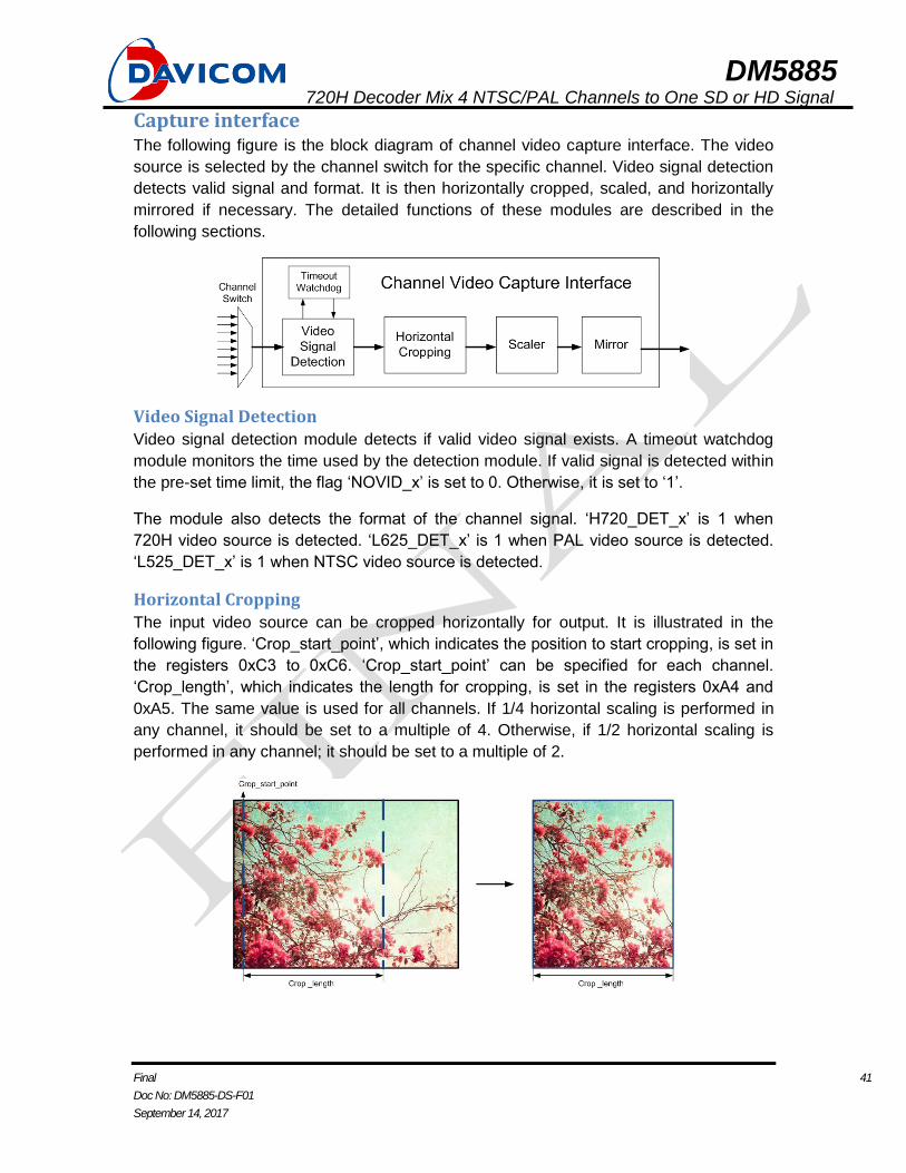
Capture interface The following figure is the block diagram of channel video capture interface. The video
source is selected by the channel switch for the specific channel. Video signal detection
detects valid signal and format. It is then horizontally cropped, scaled, and horizontally
mirrored if necessary. The detailed functions of these modules are described in the
following sections.
Video Signal Detection
Video signal detection module detects if valid video signal exists. A timeout watchdog
module monitors the time used by the detection module. If valid signal is detected within
the pre-set time limit, the flag ‘NOVID_x’ is set to 0. Otherwise, it is set to ‘1’.
The module also detects the format of the channel signal. ‘H720_DET_x’ is 1 when
720H video source is detected. ‘L625_DET_x’ is 1 when PAL video source is detected.
‘L525_DET_x’ is 1 when NTSC video source is detected.
Horizontal Cropping
The input video source can be cropped horizontally for output. It is illustrated in the
following figure. ‘Crop_start_point’, which indicates the position to start cropping, is set in
the registers 0xC3 to 0xC6. ‘Crop_start_point’ can be specified for each channel.
‘Crop_length’, which indicates the length for cropping, is set in the registers 0xA4 and
0xA5. The same value is used for all channels. If 1/4 horizontal scaling is performed in
any channel, it should be set to a multiple of 4. Otherwise, if 1/2 horizontal scaling is
performed in any channel; it should be set to a multiple of 2.
DM5885 720H Decoder Mix 4 NTSC/PAL Channels to One SD or HD Signal
Final 42
Doc No: DM5885-DS-F01
September 14, 2017
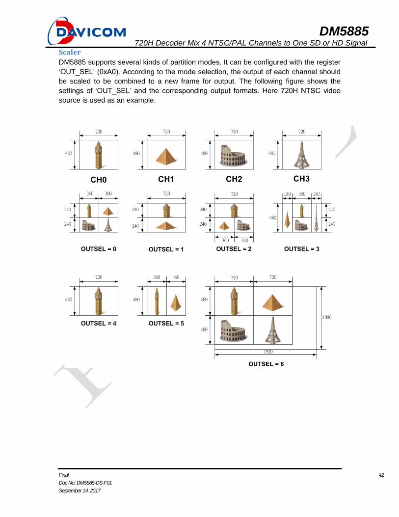
Scaler DM5885 supports several kinds of partition modes. It can be configured with the register
‘OUT_SEL’ (0xA0). According to the mode selection, the output of each channel should
be scaled to be combined to a new frame for output. The following figure shows the
settings of ‘OUT_SEL’ and the corresponding output formats. Here 720H NTSC video
source is used as an example.
DM5885 720H Decoder Mix 4 NTSC/PAL Channels to One SD or HD Signal
Final 43
Doc No: DM5885-DS-F01
September 14, 2017
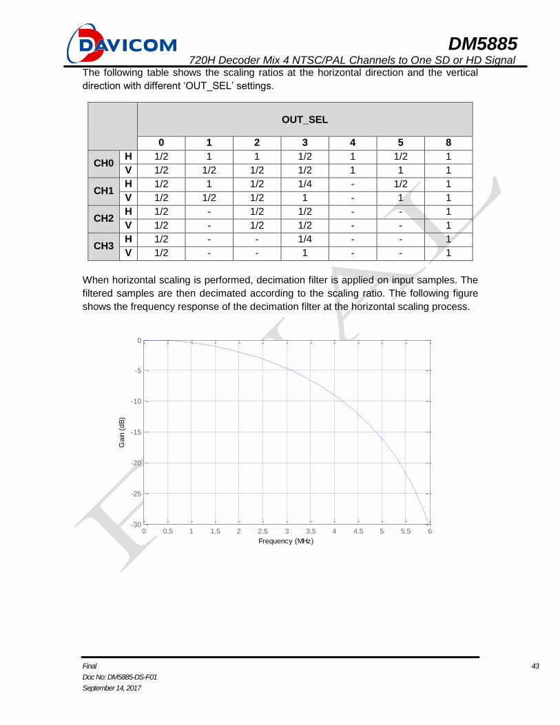
The following table shows the scaling ratios at the horizontal direction and the vertical
direction with different ‘OUT_SEL’ settings.
OUT_SEL
0 1 2 3 4 5 8
CH0 H 1/2 1 1 1/2 1 1/2 1
V 1/2 1/2 1/2 1/2 1 1 1
CH1 H 1/2 1 1/2 1/4 - 1/2 1
V 1/2 1/2 1/2 1 - 1 1
CH2 H 1/2 - 1/2 1/2 - - 1
V 1/2 - 1/2 1/2 - - 1
CH3 H 1/2 - - 1/4 - - 1
V 1/2 - - 1 - - 1
When horizontal scaling is performed, decimation filter is applied on input samples. The
filtered samples are then decimated according to the scaling ratio. The following figure
shows the frequency response of the decimation filter at the horizontal scaling process.
0 0.5 1 1.5 2 2.5 3 3.5 4 4.5 5 5.5 6-30
-25
-20
-15
-10
-5
0
Frequency (MHz)
Gain
(dB
)
DM5885 720H Decoder Mix 4 NTSC/PAL Channels to One SD or HD Signal
Final 44
Doc No: DM5885-DS-F01
September 14, 2017
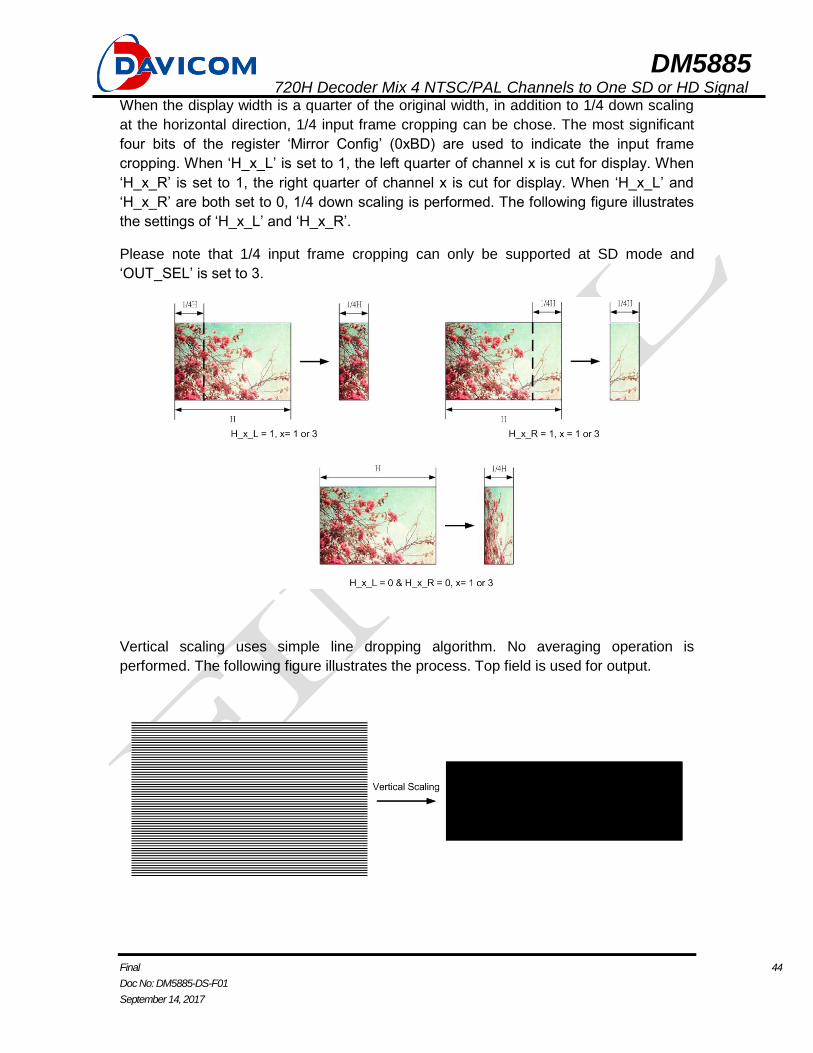
When the display width is a quarter of the original width, in addition to 1/4 down scaling
at the horizontal direction, 1/4 input frame cropping can be chose. The most significant
four bits of the register ‘Mirror Config’ (0xBD) are used to indicate the input frame
cropping. When ‘H_x_L’ is set to 1, the left quarter of channel x is cut for display. When
‘H_x_R’ is set to 1, the right quarter of channel x is cut for display. When ‘H_x_L’ and
‘H_x_R’ are both set to 0, 1/4 down scaling is performed. The following figure illustrates
the settings of ‘H_x_L’ and ‘H_x_R’.
Please note that 1/4 input frame cropping can only be supported at SD mode and
‘OUT_SEL’ is set to 3.
Vertical scaling uses simple line dropping algorithm. No averaging operation is
performed. The following figure illustrates the process. Top field is used for output.
DM5885 720H Decoder Mix 4 NTSC/PAL Channels to One SD or HD Signal
Final 45
Doc No: DM5885-DS-F01
September 14, 2017
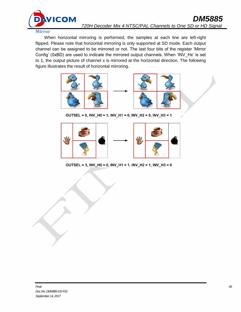
Mirror
When horizontal mirroring is performed, the samples at each line are left-right
flipped. Please note that horizontal mirroring is only supported at SD mode. Each output
channel can be assigned to be mirrored or not. The last four bits of the register ‘Mirror
Config’ (0xBD) are used to indicate the mirrored output channels. When ‘INV_Hx’ is set
to 1, the output picture of channel x is mirrored at the horizontal direction. The following
figure illustrates the result of horizontal mirroring.
DM5885 720H Decoder Mix 4 NTSC/PAL Channels to One SD or HD Signal
Final 46
Doc No: DM5885-DS-F01
September 14, 2017
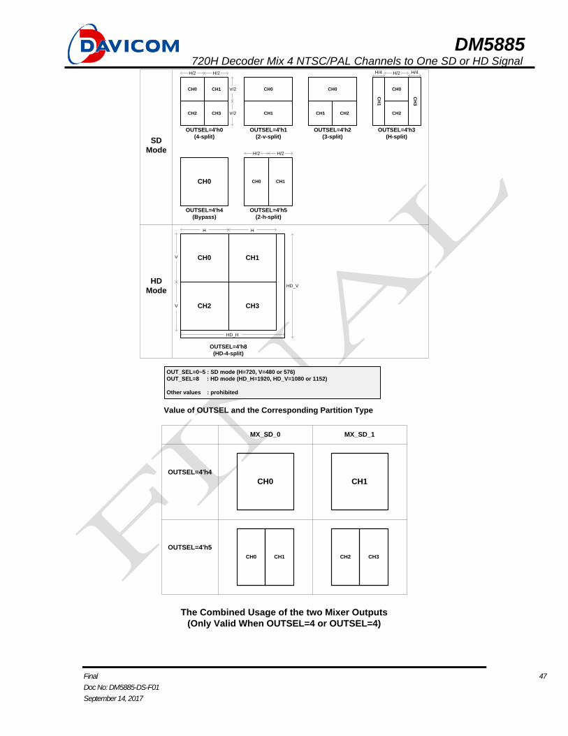
Mixer Core There are two mixer cores mixing up to four video data (CH0, CH1, CH2 and CH3)
coming from the capture interface. The mixed video is then stored into the SDRAM. The
Mixer_Core_0 is a full-function mixer supporting both HD and SD resolution.
Mixer_Core_1 is a secondary mixer which is only valid for SD mode when OUTSEL is
programmed as 4 or 5. The mixing process is determined by the value of the register
OUTSEL as shown in the following figure.
Mix-Out Interface The mix-out interface retrieves mixed video from the SDRAM. The mixed video then
goes to the chip-level output unit to form a variety of output combinations. Users are
flexible to specify the output format as progressive or interlaced. The MIX_CCIROUT_0
is the main mixer output unit supporting both SD and HD resolution. For SD mode,
MX_SD_0 is output. In case of HD mode, MX_HD_Y is output for luminance and
MX_HD_C is output for chrominance. Another mixed video MX_SD_1 from
MIX_CCIROUT_1 is available if OUTSEL is configured as 4 or 5. MX_SD_1 is always of
SD resolution. The combined usage of MIX_CCIROUT_0 and MIX_CCIROUT_1 is
shown in the following figure.
DM5885 720H Decoder Mix 4 NTSC/PAL Channels to One SD or HD Signal
Final 47
Doc No: DM5885-DS-F01
September 14, 2017
CH0 CH1
CH2 CH3
CH0
CH1
CH0
CH1 CH2
CH0
CH
1
CH2
CH
3
CH0 CH0 CH1
OUTSEL=4'h0
(4-split)
OUTSEL=4'h1
(2-v-split)
OUTSEL=4'h2
(3-split)
OUTSEL=4'h3
(H-split)
OUTSEL=4'h4
(Bypass)
OUTSEL=4'h5
(2-h-split)
OUTSEL=4'h8
(HD-4-split)
OUT_SEL=0~5 : SD mode (H=720, V=480 or 576)
OUT_SEL=8 : HD mode (HD_H=1920, HD_V=1080 or 1152)
Other values : prohibited
SD
Mode
HD
Mode
CH0 CH1
CH2 CH3
H/2 H/2
V/2
V/2
H/2H/4 H/4
H/2 H/2
V
V
HH
HD_H
HD_V
Value of OUTSEL and the Corresponding Partition Type
CH0 CH1
OUTSEL=4'h4
OUTSEL=4'h5
MX_SD_0
CH2 CH3
CH0 CH1
MX_SD_1
The Combined Usage of the two Mixer Outputs
(Only Valid When OUTSEL=4 or OUTSEL=4)
DM5885 720H Decoder Mix 4 NTSC/PAL Channels to One SD or HD Signal
Final 48
Doc No: DM5885-DS-F01
September 14, 2017
Video Rendering The output frame is divided into several partitions according to ‘OUT_SEL’. The following
table shows the coordinates of left-top point and right-bottom point of the partitions with
different values of ‘OUT_SEL’. The input video width is denoted as W and the input
video height is denoted as H.
0 1
2 3
OUT_SEL
= 0
0
1
OUT_SEL
= 1
0
1 2
OUT_SEL
= 2
1
0
2
3
OUT_SEL
= 3
0
OUT_SEL
= 4
0 1
OUT_SEL
= 5
0 1
2 3
OUT_SEL
= 8
Partition 0 (0,0) (0,0) (0,0) (W/4,0) (0,0) (0,0) (0,0)
(W/2,H/2) (W,H/2) (W,H/2) (3W/4,H/2) (W,H) (W/2,H) (W,H)
Partition 1 (W/2,0) (0,H/2) (0,H/2) (0,0) - (W/2,0) (W,0)
(W,H/2) (W,H) (W/2,H) (W/4,H) - (W,H) (2W,H)
Partition 2 (0,H/2) - (W/2,H/2) (W/4,H/2) - - (0,H)
(W/2,H) - (W,H) (3W/4,H) - - (W,2H)
Partition 3 (W/2,H/2) - - (3W/4,0) - - (W,H)
(W,H) - - (W,H) - - (2W,2H)
The output of each channel will be rendered within the active region of the
corresponding partition. The active region in each partition can be specified by defining
its top-left coordinate (COR_Xn, COR_Yn). The length of the active region is the crop
length multiplied by the scaling ratio. The vertical coordinate of the right-bottom point of
the active region is the same as that of the corresponding partition. Channel output is
horizontally shifted if the horizontal coordinate of the top-left point of the active region is
different from that of the corresponding partition. However, if the vertical coordinate of
the top-left point of the active region is different from that of the corresponding partition,
pixel lines outside the active region are discarded. The following figure illustrated the
relationship between partitions and active regions.
Several rules should be followed when specifying the coordinate (COR_Xn, COR_Yn).
DM5885 720H Decoder Mix 4 NTSC/PAL Channels to One SD or HD Signal
Final 49
Doc No: DM5885-DS-F01
September 14, 2017
1. The active region should not be outside the corresponding partition. If we define the
coordinate of the left-top point of the partition to be (S_Xn,S_Yn) and the partition
width to be PWn, the following condition should be satisified:
COR_Xn + Crop_length*H_scaling_ratio <= S_Xn + PWn
2. The settings of COR_Xn of the partitions, which have the same S_Xn, should also be
the same.
3. If S_Yn is 0, COR_Yn should also be 0.
4. The settings of COR_Yn of partitions, which have the same S_Yn, should also be the
same.
COR_XBR and COR_YBR specify the active region of the whole frame. It is
recommended that it is set to the right-bottom point of the whole frame.
When the active region is smaller than the corresponding partition, the spacing in the
region is regarded as split line. The color of the split line spacing can be assigned by the
registers: ‘Split_line_Y’, ‘Split_line_CB’, and ‘Split_line_CR’ (0xD6 to 0xD8). The default
color is white.
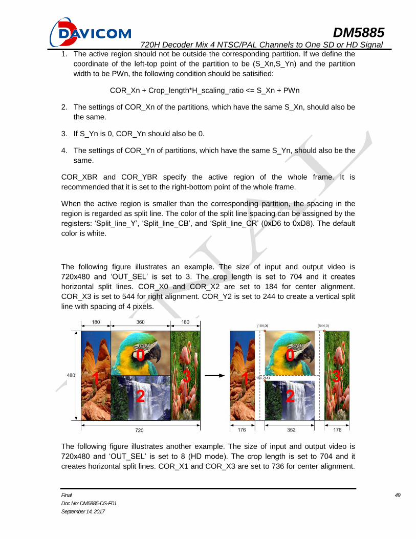
The following figure illustrates an example. The size of input and output video is
720x480 and ‘OUT_SEL’ is set to 3. The crop length is set to 704 and it creates
horizontal split lines. COR_X0 and COR_X2 are set to 184 for center alignment.
COR_X3 is set to 544 for right alignment. COR_Y2 is set to 244 to create a vertical split
line with spacing of 4 pixels.
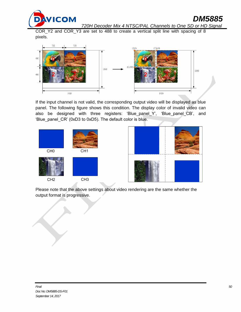
The following figure illustrates another example. The size of input and output video is
720x480 and ‘OUT_SEL’ is set to 8 (HD mode). The crop length is set to 704 and it
creates horizontal split lines. COR_X1 and COR_X3 are set to 736 for center alignment.
DM5885 720H Decoder Mix 4 NTSC/PAL Channels to One SD or HD Signal
Final 50
Doc No: DM5885-DS-F01
September 14, 2017
COR_Y2 and COR_Y3 are set to 488 to create a vertical split line with spacing of 8
pixels.
If the input channel is not valid, the corresponding output video will be displayed as blue
panel. The following figure shows this condition. The display color of invalid video can
also be designed with three registers: ‘Blue_panel_Y’, ‘Blue_panel_CB’, and
‘Blue_panel_CR’ (0xD3 to 0xD5). The default color is blue.
Please note that the above settings about video rendering are the same whether the
output format is progressive.
DM5885 720H Decoder Mix 4 NTSC/PAL Channels to One SD or HD Signal
Final 51
Doc No: DM5885-DS-F01
September 14, 2017
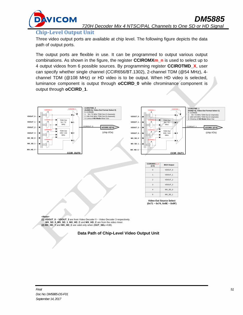
Chip-Level Output Unit Three video output ports are available at chip level. The following figure depicts the data
path of output ports.
The output ports are flexible in use. It can be programmed to output various output
combinations. As shown in the figure, the register CCIROMXm_n is used to select up to
4 output videos from 6 possible sources. By programming register CCIROTMD_X, user
can specify whether single channel (CCIR656/BT.1302), 2-channel TDM (@54 MHz), 4-
channel TDM (@108 MHz) or HD video is to be output. When HD video is selected,
luminance component is output through oCCIRD_0 while chrominance component is
output through oCCIRD_1.
CCIROUT_0
MX_SD_1
MX_SD_0
VDOUT_3
VDOUT_2
VDOUT_1
VDOUT_0
CCIR_OUT0
CCIROTMD_0
Data Path of Chip-Level Video Output Unit
CCIROTMD_0
(0x68[5:4], Video-Out Format Select 0)
0: CCIR656
1: 54 / 72 MHz TDM Out (2 channels)
2: 108 /144 MHz TDM Out (4 channels)
3: Luma of HD Mode Mixer Out
CCIROTMD_1
(0x68[7:6], Video-Out Format Select 1)
0: CCIR656
1: 54 / 72 MHz TDM Out (2 channels)
2: 108 /144 MHz TDM Out (4 channels)
3: Chroma of HD Mode Mixer Out
CCIROMXm_n
[2:0]
0
1
2
3
5
MUX Output
VDOUT_0
VDOUT_1
VDOUT_2
VDOUT_3
MX_SD_1
Video-Out Source Select
(0x71 ~ 0x74, 0x9E ~ 0x9F)
(chip I/Os)
TDM Out
54 / 72
MHz
TDM Out
108 / 144
MHz
MX_HD_Y
CCIROMX0_0
CCIROMX0_1
CCIROMX0_2
CCIROMX0_3
0
1
2
3
oCCIRD_0[7:0]CCIROUT_1
MX_SD_1
MX_SD_0
VDOUT_3
VDOUT_2
VDOUT_1
VDOUT_0
CCIR_OUT1
CCIROTMD_1
(chip I/Os)
TDM Out
54 / 72
MHz
TDM Out
108 / 144
MHz
MX_HD_C
CCIROMX1_1
CCIROMX1_0
CCIROMX1_2
CCIROMX1_3
0
1
2
3
oCCIRD_1[7:0]
4 MX_SD_0
<Note>
(1) VDOUT_0 ~ VDOUT_3 are from Video Decoder 0 ~ Video Decoder 3 respectively.
MX_SD_0, MX_SD_1, MX_HD_C and MX_HD_C are from the video mixer.
(2) MX_HD_Y and MX_HD_C are valid only when (OUT_SEL=4'd8).
DM5885 720H Decoder Mix 4 NTSC/PAL Channels to One SD or HD Signal
Final 52
Doc No: DM5885-DS-F01
September 14, 2017
Internal Control Registers Note: Take 8’h64 for example – 8’= bit / h=hex / 64=value
System Control
Address= 8’h64
System Control Page
7-bit 6-bit 5-bit 4-bit 3-bit 2-bit 1-bit 0-bit
0 0 0 0 0 0 0 1
PAGE_3 PAGE_2 PAGE_1 PAGE_0
PAGE_0: VD space 0, to access VD_0 register please program this bit to 1.
PAGE_1: VD space 1, to access VD_1 register please program this bit to 1.
PAGE_2: VD space 2, to access VD_2 register please program this bit to 1.
PAGE_3: VD space 3, to access VD_3 register please program this bit to 1.
In case of register read, only one of the four bits can be set to 1.
Address= 8’h65
System Reset
7-bit 6-bit 5-bit 4-bit 3-bit 2-bit 1-bit 0-bit
0 0 0 0 0 0 0 0
RSTZ TRSTZ
TRSTZ: When 1, reset whole chip except SW PLL, GPIO and Device ID setting. (WO)
RSTZ: When 1, reset all video decoders, mixer, TDM and audio interface. It also
resets video decoder configurations.
DM5885 720H Decoder Mix 4 NTSC/PAL Channels to One SD or HD Signal
Final 53
Doc No: DM5885-DS-F01
September 14, 2017
Address= 8’h66
Global INT Mask
7-bit 6-bit 5-bit 4-bit 3-bit 2-bit 1-bit 0-bit
0 0 0 0 0 0 0 0
VDMASK_3
VDMASK_2
VDMASK_1
VDMASK_0
VDMASK_0: Enable INT from VD_0.
VDMASK_1: Enable INT from VD_1.
VDMASK_2: Enable INT from VD_2.
VDMASK_3: Enable INT from VD_3.
Address= 8’h67
Global INT Status
7-bit 6-bit 5-bit 4-bit 3-bit 2-bit 1-bit 0-bit
0 0 0 0 0 0 0 0
VDINT_3 VDINT_2 VDINT_1 VDINT_0
VDINT_0: VD_0 INT status. (RO)
VDINT_1: VD_1 INT status. (RO)
VDINT_2: VD_2 INT status. (RO)
VDINT_3: VD_3 INT status. (RO)
DM5885 720H Decoder Mix 4 NTSC/PAL Channels to One SD or HD Signal
Final 54
Doc No: DM5885-DS-F01
September 14, 2017
Address= 8’h68
CCIR656 IO Control
7-bit 6-bit 5-bit 4-bit 3-bit 2-bit 1-bit 0-bit
2’h0 2’h0 0 0 0 0
CCIROTMD_1 CCIROTMD_0 CCIROE_3
CCIROE_2
CCIROE_1
CCIROE_0
CCIROE_0: Chip CCIR656_0 related 9 pins output enable.
When 1, output mode. When 0, input mode.
CCIROE_1: Chip CCIR656_1 related 9 pins output enable.
When 1, output mode. When 0, input mode.
CCIROE_2: Chip CCIR656_2 related 9 pins output enable.
When 1, output mode. When 0, input mode.
CCIROE_3: Chip CCIR656_3 related 9 pins output enable.
When 1, output mode. When 0, input mode.
CCIROTMD_0: Chip CCUROUT_0 output Mode type.
2’h0: CCIR656 output mode.
2’h1: 54Mhz TDM mode with D1 resolution for each channel.
2’h2: 108Mhz TDM mode with D1 resolution for each channel.
2’h3: HD Mixer mode with Y data bus.
CCIROTMD_1: Chip CCUROUT_1 output Mode type.
2’h0: CCIR656 output mode.
2’h1: 54Mhz TDM mode with D1 resolution for each channel.
2’h2: 108Mhz TDM mode with D1 resolution for each channel.
2’h3: HD Mixer mode with C data bus.
DM5885 720H Decoder Mix 4 NTSC/PAL Channels to One SD or HD Signal
Final 55
Doc No: DM5885-DS-F01
September 14, 2017
Address= 8’h69
PIXCLK Polarity
7-bit 6-bit 5-bit 4-bit 3-bit 2-bit 1-bit 0-bit
0 0 0 0 0 0 0 0
OPIXCLK3_INV
OPIXCLK2_INV
OPIXCLK1_INV
OPIXCLK0_INV
OPIXCLK4_INV
IPIXCLK_INV
IPIXCLKOE
IPIXCLK_OE: The polarity of pin No.54.
When 1: pin No.54 is output pin and drives VD_INT signals to pin.
When 0: pin No.54 is input pin and receives iTDM pixclk.
IPIXCLK_INV: When 1, inverse iTDM pixclk to internal logic.
OPIXCLK4_INV: When 1, inverse output pixclk of CCIROUT_4.
OPIXCLK0_INV: When 1, inverse output pixclk of CCIROUT_0.
OPIXCLK1_INV: When 1, inverse output pixclk of CCIROUT_1.
OPIXCLK2_INV: When 1, inverse output pixclk of CCIROUT_2.
OPIXCLK3_INV: When 1, inverse output pixclk of CCIROUT_3.
Address= 8’h6A
IC Mode Control
7-bit 6-bit 5-bit 4-bit 3-bit 2-bit 1-bit 0-bit
0 0 0 0 2’h2 2’h0
PINCFG CLKADCOPT
CLKADCOPT: The VADC_1 input clock selection. (108MHz)
2’h0: The default value, sources from PLL1.
2’h1: Clock sources from PLL2.
2’h2: Clock source from chip pin NO.126.
DM5885 720H Decoder Mix 4 NTSC/PAL Channels to One SD or HD Signal
Final 56
Doc No: DM5885-DS-F01
September 14, 2017
PINCFG: IC pin mode option.
Set 2’h0 for Video decoder x4 without Mixer.
Set 2’h1 for Video decoder x4 with Mixer.
Set 2’h3 for Video decoder x4 with Mixer. (Alternative pin assignment)
Address= 8’h6B
Output Pixclk Delay Configuration
7-bit 6-bit 5-bit 4-bit 3-bit 2-bit 1-bit 0-bit
0 3’h0 0 3’h0
DLYMUX_PIXCLK1 DLYMUX_PIXCLK0
DYLMUX_PIXCLK0: Programmable pixclk delay of CCIROUT_0.
(3’h0: zero delay 3’h7: max delay, add 0.6ns at every step)
DYLMUX_PIXCLK1: Programmable pixclk delay of CCIROUT_1.
(3’h0: zero delay 3’h7: max delay, add 0.6ns at every step)
DM5885 720H Decoder Mix 4 NTSC/PAL Channels to One SD or HD Signal
Final 57
Doc No: DM5885-DS-F01
September 14, 2017
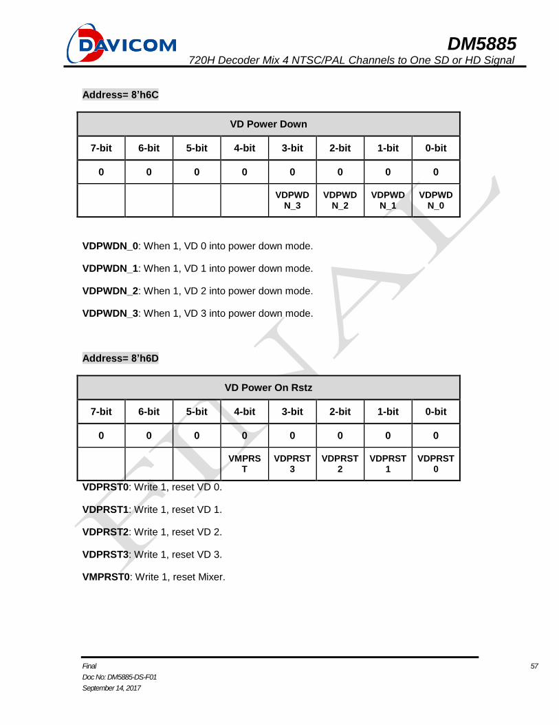
Address= 8’h6C
VD Power Down
7-bit 6-bit 5-bit 4-bit 3-bit 2-bit 1-bit 0-bit
0 0 0 0 0 0 0 0
VDPWDN_3
VDPWDN_2
VDPWDN_1
VDPWDN_0
VDPWDN_0: When 1, VD 0 into power down mode.
VDPWDN_1: When 1, VD 1 into power down mode.
VDPWDN_2: When 1, VD 2 into power down mode.
VDPWDN_3: When 1, VD 3 into power down mode.
Address= 8’h6D
VD Power On Rstz
7-bit 6-bit 5-bit 4-bit 3-bit 2-bit 1-bit 0-bit
0 0 0 0 0 0 0 0
VMPRST
VDPRST3
VDPRST2
VDPRST1
VDPRST0
VDPRST0: Write 1, reset VD 0.
VDPRST1: Write 1, reset VD 1.
VDPRST2: Write 1, reset VD 2.
VDPRST3: Write 1, reset VD 3.
VMPRST0: Write 1, reset Mixer.
DM5885 720H Decoder Mix 4 NTSC/PAL Channels to One SD or HD Signal
Final 58
Doc No: DM5885-DS-F01
September 14, 2017
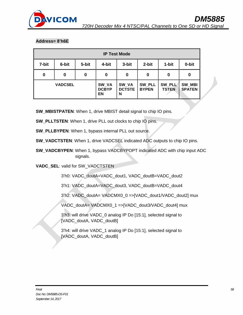
Address= 8’h6E
IP Test Mode
7-bit 6-bit 5-bit 4-bit 3-bit 2-bit 1-bit 0-bit
0 0 0 0 0 0 0 0
VADCSEL SW_VADCBYPEN
SW_VADCTSTEN
SW_PLLBYPEN
SW_PLLTSTEN
SW_MBISPATEN
SW_MBISTPATEN: When 1, drive MBIST detail signal to chip IO pins.
SW_PLLTSTEN: When 1, drive PLL out clocks to chip IO pins.
SW_PLLBYPEN: When 1, bypass internal PLL out source.
SW_VADCTSTEN: When 1, drive VADCSEL indicated ADC outputs to chip IO pins.
SW_VADCBYPEN: When 1, bypass VADCBYPOPT indicated ADC with chip input ADC
signals.
VADC_SEL: valid for SW_VADCTSTEN
3’h0: VADC_doutA=VADC_dout1, VADC_doutB=VADC_dout2
3’h1: VADC_doutA=VADC_dout3, VADC_doutB=VADC_dout4
3’h2: VADC_doutA= VADCMX0_0 =>[VADC_dout1/VADC_dout2] mux
VADC_doutA= VADCMX0_1 =>[VADC_dout3/VADC_dout4] mux
3’h3: will drive VADC_0 analog IP Do [15:1], selected signal to
[VADC_doutA, VADC_doutB]
3’h4: will drive VADC_1 analog IP Do [15:1], selected signal to
[VADC_doutA, VADC_doutB]
DM5885 720H Decoder Mix 4 NTSC/PAL Channels to One SD or HD Signal
Final 59
Doc No: DM5885-DS-F01
September 14, 2017
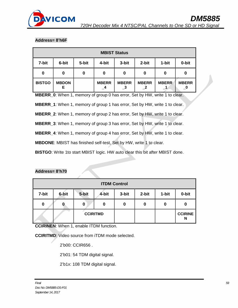
Address= 8’h6F
MBIST Status
7-bit 6-bit 5-bit 4-bit 3-bit 2-bit 1-bit 0-bit
0 0 0 0 0 0 0 0
BISTGO MBDONE
MBERR_4
MBERR_3
MBERR_2
MBERR_1
MBERR_0
MBERR_0: When 1, memory of group 0 has error, Set by HW, write 1 to clear.
MBERR_1: When 1, memory of group 1 has error, Set by HW, write 1 to clear.
MBERR_2: When 1, memory of group 2 has error, Set by HW, write 1 to clear.
MBERR_3: When 1, memory of group 3 has error, Set by HW, write 1 to clear.
MBERR_4: When 1, memory of group 4 has error, Set by HW, write 1 to clear.
MBDONE: MBIST has finished self-test, Set by HW, write 1 to clear.
BISTGO: Write 1to start MBIST logic. HW auto clear this bit after MBIST done.
Address= 8’h70
ITDM Control
7-bit 6-bit 5-bit 4-bit 3-bit 2-bit 1-bit 0-bit
0 0 0 0 0 0 0 0
CCIRITMD CCIRINEN
CCIRINEN: When 1, enable ITDM function.
CCIRITMD: Video source from iTDM mode selected.
2’b00: CCIR656 .
2’b01: 54 TDM digital signal.
2’b1x: 108 TDM digital signal.
DM5885 720H Decoder Mix 4 NTSC/PAL Channels to One SD or HD Signal
Final 60
Doc No: DM5885-DS-F01
September 14, 2017
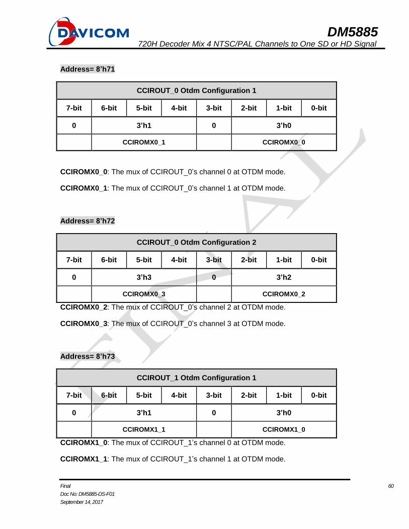
Address= 8’h71
CCIROUT_0 Otdm Configuration 1
7-bit 6-bit 5-bit 4-bit 3-bit 2-bit 1-bit 0-bit
0 3’h1 0 3’h0
CCIROMX0_1 CCIROMX0_0
CCIROMX0_0: The mux of CCIROUT_0’s channel 0 at OTDM mode.
CCIROMX0_1: The mux of CCIROUT_0’s channel 1 at OTDM mode.
Address= 8’h72
CCIROUT_0 Otdm Configuration 2
7-bit 6-bit 5-bit 4-bit 3-bit 2-bit 1-bit 0-bit
0 3’h3 0 3’h2
CCIROMX0_3 CCIROMX0_2
CCIROMX0_2: The mux of CCIROUT_0’s channel 2 at OTDM mode.
CCIROMX0_3: The mux of CCIROUT_0’s channel 3 at OTDM mode.
Address= 8’h73
CCIROUT_1 Otdm Configuration 1
7-bit 6-bit 5-bit 4-bit 3-bit 2-bit 1-bit 0-bit
0 3’h1 0 3’h0
CCIROMX1_1 CCIROMX1_0
CCIROMX1_0: The mux of CCIROUT_1’s channel 0 at OTDM mode.
CCIROMX1_1: The mux of CCIROUT_1’s channel 1 at OTDM mode.
DM5885 720H Decoder Mix 4 NTSC/PAL Channels to One SD or HD Signal
Final 61
Doc No: DM5885-DS-F01
September 14, 2017
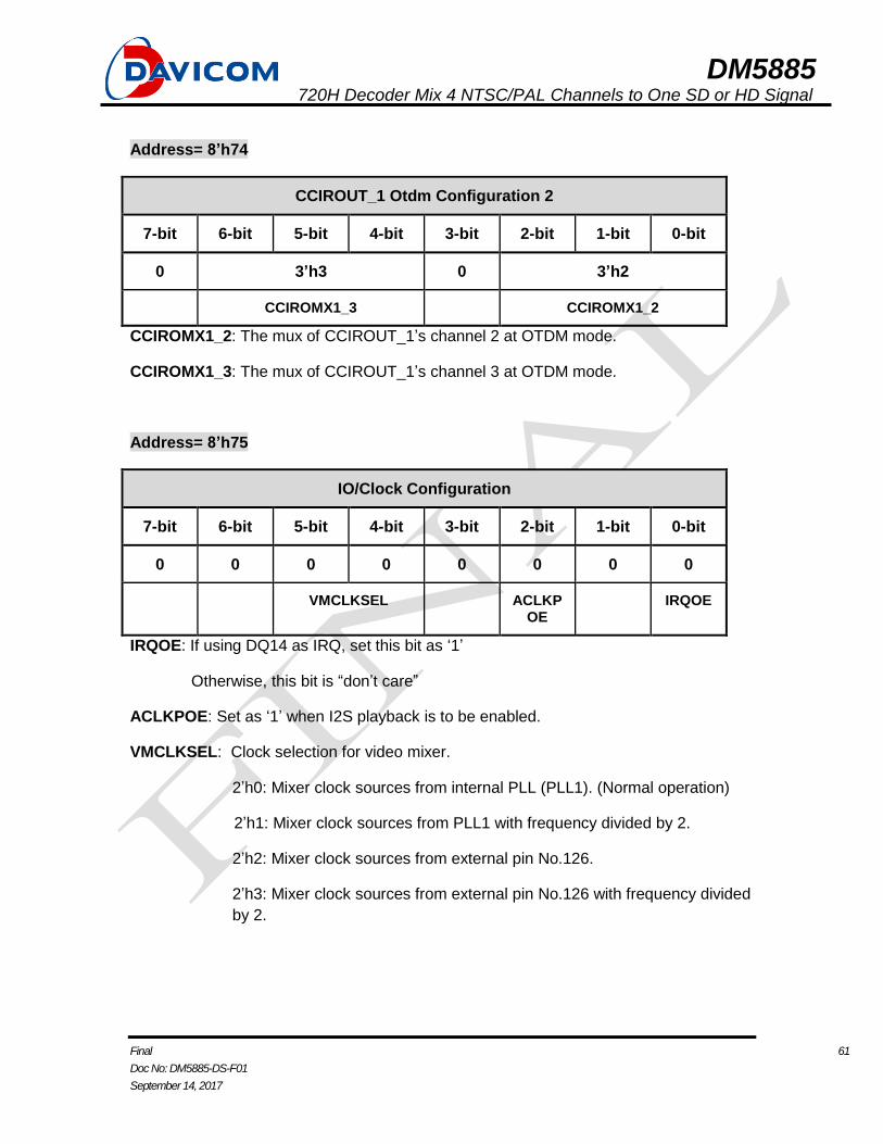
Address= 8’h74
CCIROUT_1 Otdm Configuration 2
7-bit 6-bit 5-bit 4-bit 3-bit 2-bit 1-bit 0-bit
0 3’h3 0 3’h2
CCIROMX1_3 CCIROMX1_2
CCIROMX1_2: The mux of CCIROUT_1’s channel 2 at OTDM mode.
CCIROMX1_3: The mux of CCIROUT_1’s channel 3 at OTDM mode.
Address= 8’h75
IO/Clock Configuration
7-bit 6-bit 5-bit 4-bit 3-bit 2-bit 1-bit 0-bit
0 0 0 0 0 0 0 0
VMCLKSEL ACLKPOE
IRQOE
IRQOE: If using DQ14 as IRQ, set this bit as ‘1’
Otherwise, this bit is “don’t care”
ACLKPOE: Set as ‘1’ when I2S playback is to be enabled.
VMCLKSEL: Clock selection for video mixer.
2’h0: Mixer clock sources from internal PLL (PLL1). (Normal operation)
2’h1: Mixer clock sources from PLL1 with frequency divided by 2.
2’h2: Mixer clock sources from external pin No.126.
2’h3: Mixer clock sources from external pin No.126 with frequency divided
by 2.

DM5885 720H Decoder Mix 4 NTSC/PAL Channels to One SD or HD Signal
Final 62
Doc No: DM5885-DS-F01
September 14, 2017
Address= 8’h77
CHIP Status
7-bit 6-bit 5-bit 4-bit 3-bit 2-bit 1-bit 0-bit
0 0 0 0 0 0 0 0
PWRON
PWRON: Power On status. (RO)
Address= 8’h78
I2C Master Configuration
7-bit 6-bit 5-bit 4-bit 3-bit 2-bit 1-bit 0-bit
8’hB8
CH device address
CH0~CH3: i2c slave device address. (R/W)
-DM5885 device address will be {4’hC,4’h0}
-I2CMaster_0: device address will be {4’hC,4’h2}
-I2CMaster_1: device address will be {4’hC,4’h4}
-I2CMaster_2: device address will be {4’hC,4’h6}
-I2CMaster_3: device address will be {4’hC,4’h8}
-For broadcast I2CMaster_CH0~I2CMaster_CH3, device address
{4’HC,4’HE}
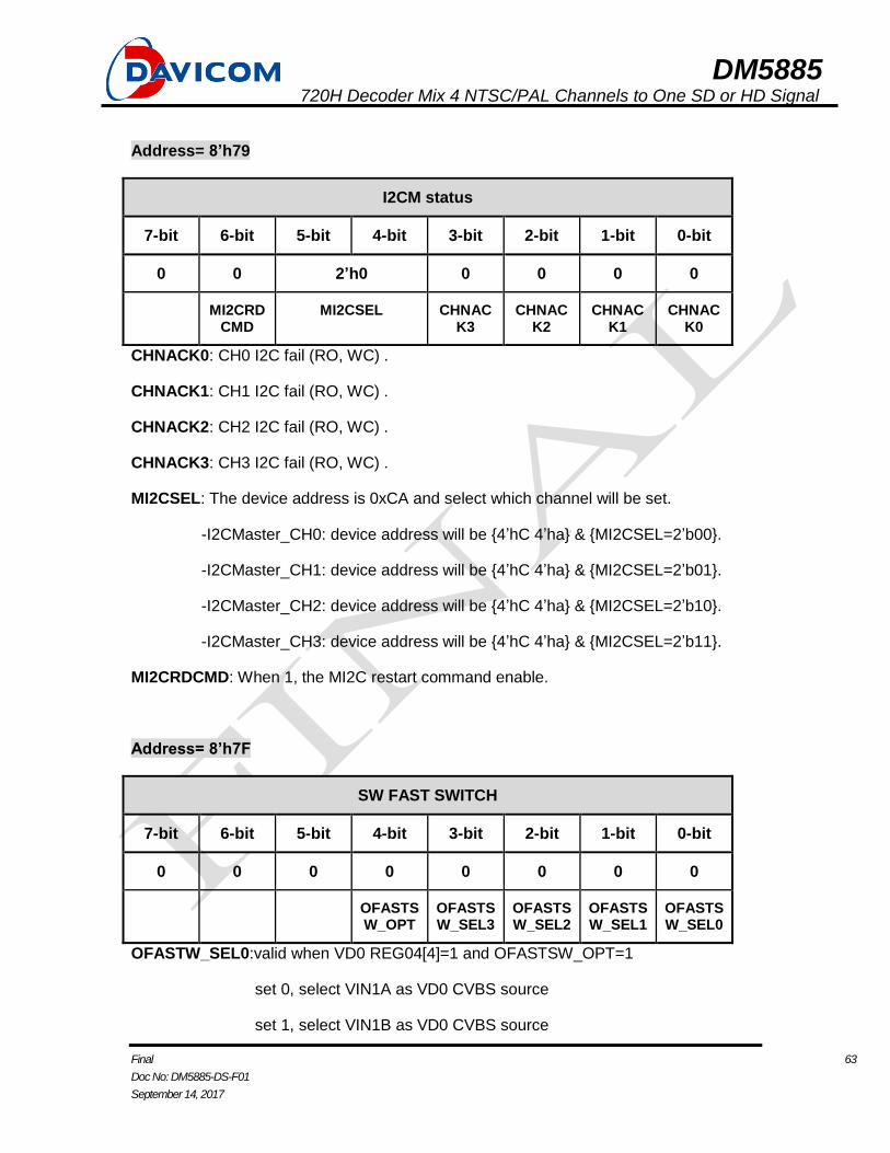
DM5885 720H Decoder Mix 4 NTSC/PAL Channels to One SD or HD Signal
Final 63
Doc No: DM5885-DS-F01
September 14, 2017
Address= 8’h79
I2CM status
7-bit 6-bit 5-bit 4-bit 3-bit 2-bit 1-bit 0-bit
0 0 2’h0 0 0 0 0
MI2CRDCMD
MI2CSEL CHNACK3
CHNACK2
CHNACK1
CHNACK0
CHNACK0: CH0 I2C fail (RO, WC) .
CHNACK1: CH1 I2C fail (RO, WC) .
CHNACK2: CH2 I2C fail (RO, WC) .
CHNACK3: CH3 I2C fail (RO, WC) .
MI2CSEL: The device address is 0xCA and select which channel will be set.
-I2CMaster_CH0: device address will be {4’hC 4’ha} & {MI2CSEL=2’b00}.
-I2CMaster_CH1: device address will be {4’hC 4’ha} & {MI2CSEL=2’b01}.
-I2CMaster_CH2: device address will be {4’hC 4’ha} & {MI2CSEL=2’b10}.
-I2CMaster_CH3: device address will be {4’hC 4’ha} & {MI2CSEL=2’b11}.
MI2CRDCMD: When 1, the MI2C restart command enable.
Address= 8’h7F
SW FAST SWITCH
7-bit 6-bit 5-bit 4-bit 3-bit 2-bit 1-bit 0-bit
0 0 0 0 0 0 0 0
OFASTSW_OPT
OFASTSW_SEL3
OFASTSW_SEL2
OFASTSW_SEL1
OFASTSW_SEL0
OFASTW_SEL0:valid when VD0 REG04[4]=1 and OFASTSW_OPT=1
set 0, select VIN1A as VD0 CVBS source
set 1, select VIN1B as VD0 CVBS source
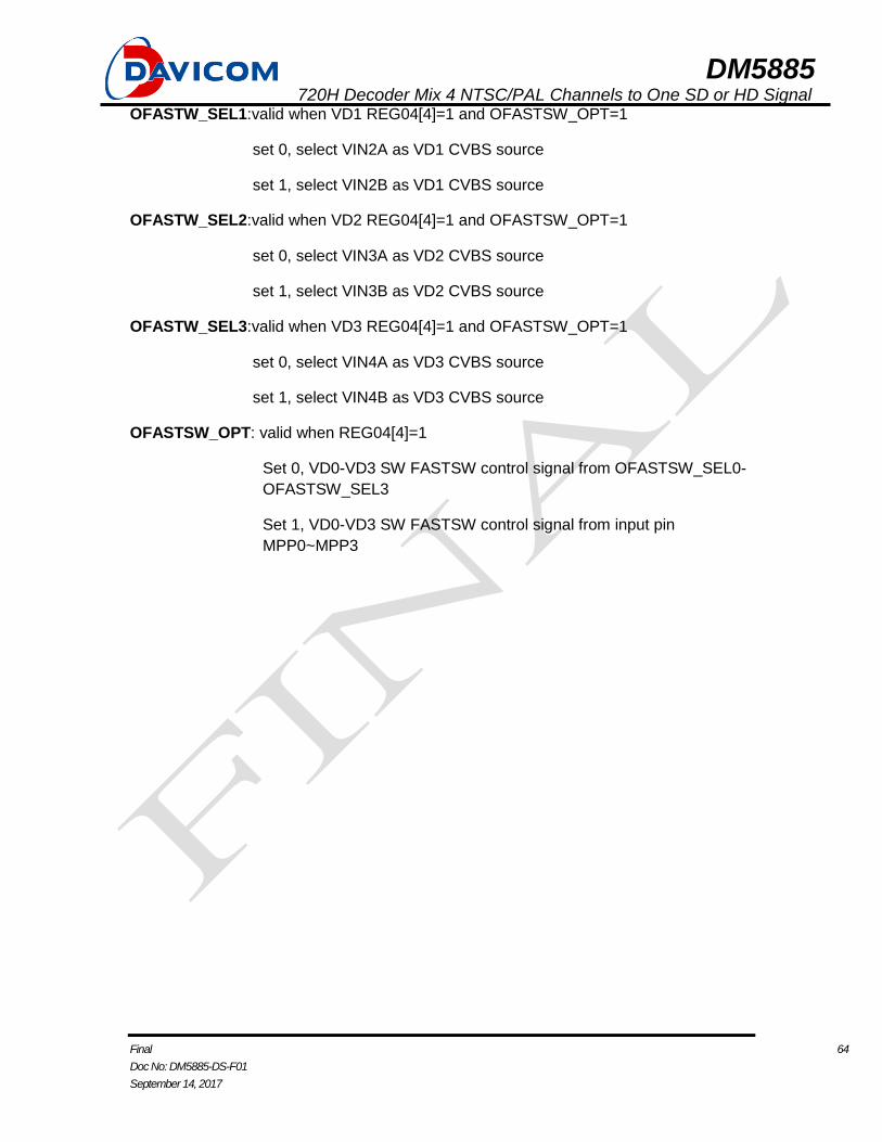
DM5885 720H Decoder Mix 4 NTSC/PAL Channels to One SD or HD Signal
Final 64
Doc No: DM5885-DS-F01
September 14, 2017
OFASTW_SEL1:valid when VD1 REG04[4]=1 and OFASTSW_OPT=1
set 0, select VIN2A as VD1 CVBS source
set 1, select VIN2B as VD1 CVBS source
OFASTW_SEL2:valid when VD2 REG04[4]=1 and OFASTSW_OPT=1
set 0, select VIN3A as VD2 CVBS source
set 1, select VIN3B as VD2 CVBS source
OFASTW_SEL3:valid when VD3 REG04[4]=1 and OFASTSW_OPT=1
set 0, select VIN4A as VD3 CVBS source
set 1, select VIN4B as VD3 CVBS source
OFASTSW_OPT: valid when REG04[4]=1
Set 0, VD0-VD3 SW FASTSW control signal from OFASTSW_SEL0-
OFASTSW_SEL3
Set 1, VD0-VD3 SW FASTSW control signal from input pin
MPP0~MPP3
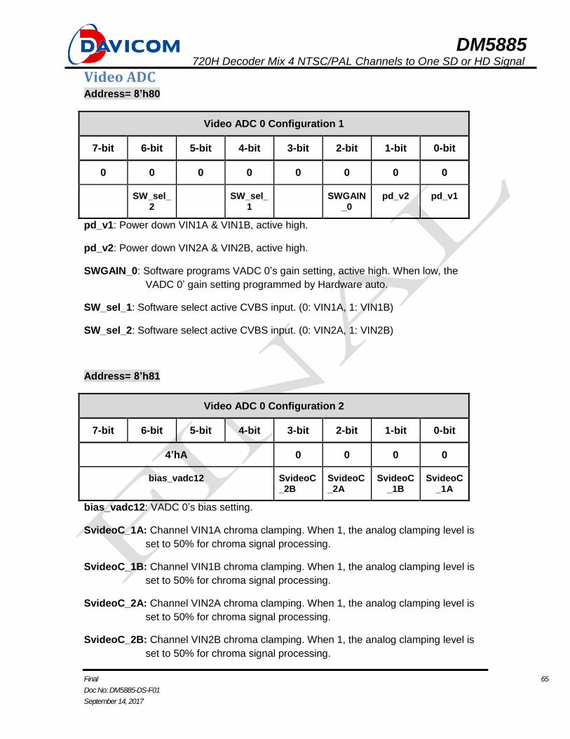
DM5885 720H Decoder Mix 4 NTSC/PAL Channels to One SD or HD Signal
Final 65
Doc No: DM5885-DS-F01
September 14, 2017
Video ADC Address= 8’h80
Video ADC 0 Configuration 1
7-bit 6-bit 5-bit 4-bit 3-bit 2-bit 1-bit 0-bit
0 0 0 0 0 0 0 0
SW_sel_2
SW_sel_1
SWGAIN_0
pd_v2 pd_v1
pd_v1: Power down VIN1A & VIN1B, active high.
pd_v2: Power down VIN2A & VIN2B, active high.
SWGAIN_0: Software programs VADC 0’s gain setting, active high. When low, the
VADC 0’ gain setting programmed by Hardware auto.
SW_sel_1: Software select active CVBS input. (0: VIN1A, 1: VIN1B)
SW_sel_2: Software select active CVBS input. (0: VIN2A, 1: VIN2B)
Address= 8’h81
Video ADC 0 Configuration 2
7-bit 6-bit 5-bit 4-bit 3-bit 2-bit 1-bit 0-bit
4’hA 0 0 0 0
bias_vadc12 SvideoC_2B
SvideoC_2A
SvideoC_1B
SvideoC_1A
bias_vadc12: VADC 0’s bias setting.
SvideoC_1A: Channel VIN1A chroma clamping. When 1, the analog clamping level is
set to 50% for chroma signal processing.
SvideoC_1B: Channel VIN1B chroma clamping. When 1, the analog clamping level is
set to 50% for chroma signal processing.
SvideoC_2A: Channel VIN2A chroma clamping. When 1, the analog clamping level is
set to 50% for chroma signal processing.
SvideoC_2B: Channel VIN2B chroma clamping. When 1, the analog clamping level is
set to 50% for chroma signal processing.
DM5885 720H Decoder Mix 4 NTSC/PAL Channels to One SD or HD Signal
Final 66
Doc No: DM5885-DS-F01
September 14, 2017
Address= 8’h82
Video ADC 0 Configuration 3
7-bit 6-bit 5-bit 4-bit 3-bit 2-bit 1-bit 0-bit
0 0 0 0 0 0 0 0
SW_gain1B SW_gain1A
SW_gain1A: VIN1A’s gain value, valid when REG80[2]=1.
SW_gain1B: VIN1B’s gain value, valid when REG80[2]=1.
Minimum gain is set by 4’h0. Maximum gain is set by 4’hf.
The characteristic is the same as REG83
Address= 8’h83
Video ADC 0 Configuration 4
7-bit 6-bit 5-bit 4-bit 3-bit 2-bit 1-bit 0-bit
0 0 0 0 0 0 0 0
SW_gain2B SW_gain2A
SW_gain2A: VIN2A’s gain value, valid when REG80[2]=1.
SW_gain2B: VIN2B’s gain value, valid when REG80[2]=1.
DM5885 720H Decoder Mix 4 NTSC/PAL Channels to One SD or HD Signal
Final 67
Doc No: DM5885-DS-F01
September 14, 2017
Address= 8’h84
Video ADC 0 Configuration 5
7-bit 6-bit 5-bit 4-bit 3-bit 2-bit 1-bit 0-bit
0 0 0 0 0 0 0 0
clmp1B clmp1A
Clmp1A: VIN1A’s clamp value.
Clmp1B: VIN1B’s clamp value.
The clamp can be used to adjust the sync tip value to the nominal value of 20.
Address= 8’h85
Video ADC 0 Configuration 6
7-bit 6-bit 5-bit 4-bit 3-bit 2-bit 1-bit 0-bit
0 0 0 0 0 0 0 0
Clmp2B clmp2A
Clmp2A: VIN2A’s clamp value.
Clmp2B: VIN2B’s clamp value.
Address= 8’h86
Video ADC 1 Configuration 1
7-bit 6-bit 5-bit 4-bit 3-bit 2-bit 1-bit 0-bit
0 0 0 0 0 0 0 0
SW_sel_4
SW_sel_3
SWGAIN_1
pd_v4 pd_v3
pd_v3: Power down VIN3A & VIN3B, active high.
pd_v4: Power down VIN4A & VIN4B, active high.
DM5885 720H Decoder Mix 4 NTSC/PAL Channels to One SD or HD Signal
Final 68
Doc No: DM5885-DS-F01
September 14, 2017
SWGAIN_1: Software programs VADC 1’s gain setting, active high. When low, the
VADC 1’ gain setting programmed by Hardware auto.
SW_sel_3: Software select active CVBS input. (0: VIN3A, 1: VIN3B)
SW_sel_4: Software select active CVBS input. (0: VIN4A, 1: VIN4B)
Address= 8’h87
Video ADC 1 Configuration 2
7-bit 6-bit 5-bit 4-bit 3-bit 2-bit 1-bit 0-bit
4’hA 0 0 0 0
bias_vadc34 SvideoC_4B
SvideoC_4A
SvideoC_3B
SvideoC_3A
bias_vadc34: VADC 1’s bias setting.
SvideoC_3A: Channel VIN3A chroma clamping. When 1, the analog clamping level is
set to 50% for chroma signal processing.
SvideoC_3B: Channel VIN3B chroma clamping. When 1, the analog clamping level is
set to 50% for chroma signal processing.
SvideoC_4A: Channel VIN4A chroma clamping. When 1, the analog clamping level is
set to 50% for chroma signal processing.
SvideoC_4B: Channel VIN4B chroma clamping. When 1, the analog clamping level is
set to 50% for chroma signal processing.
DM5885 720H Decoder Mix 4 NTSC/PAL Channels to One SD or HD Signal
Final 69
Doc No: DM5885-DS-F01
September 14, 2017
Address= 8’h88
Video ADC 1 Configuration 3
7-bit 6-bit 5-bit 4-bit 3-bit 2-bit 1-bit 0-bit
0 0 0 0 0 0 0 0
SW_gain3B SW_gain3A
SW_gain3A: VIN3A’s gain value, valid when REG86[2]=1.
SW_gain3B: VIN3B’s gain value, valid when REG86[2]=1.
Address= 8’h89
Video ADC 1 Configuration 4
7-bit 6-bit 5-bit 4-bit 3-bit 2-bit 1-bit 0-bit
0 0 0 0 0 0 0 0
SW_gain4B SW_gain4A
SW_gain4A: VIN4A’s gain value, valid when REG86[2]=1.
SW_gain4B: VIN4B’s gain value, valid when REG86[2]=1.
Address= 8’h8A
Video ADC 1 Configuration 5
7-bit 6-bit 5-bit 4-bit 3-bit 2-bit 1-bit 0-bit
0 0 0 0 0 0 0 0
Clmp3B Clmp3A
Clmp3A: VIN3A’s clamp value.
Clmp3B: VIN3B’s clamp value.
DM5885 720H Decoder Mix 4 NTSC/PAL Channels to One SD or HD Signal
Final 70
Doc No: DM5885-DS-F01
September 14, 2017
Address= 8’h8B
Video ADC 1 Configuration 6
7-bit 6-bit 5-bit 4-bit 3-bit 2-bit 1-bit 0-bit
0 0 0 0 0 0 0 0
Clmp4B Clmp4A
Clmp4A: VIN4A’s clamp value.
Clmp4B: VIN4B’s clamp value.
Address= 8’h8C
Video ADC LPF Option
7-bit 6-bit 5-bit 4-bit 3-bit 2-bit 1-bit 0-bit
0 0 0 0 2’h0 2’h0
lpf_34 lpf_12
lpf_12: VADC 0 LPF selected.
lpf_34: VADC 1 LPF selected.
lpf_xx: 2’h0: 6MHz
2’h1: 9MHz
Others: bypass
Address= 8’h8D
VADC Clk Delay Configuration 1
7-bit 6-bit 5-bit 4-bit 3-bit 2-bit 1-bit 0-bit
0 3’h0 0 3’h0
DLYMUX_ANA34 DLYMUX_ANA12
DM5885 720H Decoder Mix 4 NTSC/PAL Channels to One SD or HD Signal
Final 71
Doc No: DM5885-DS-F01
September 14, 2017
DLYMUX_ANA12: Programmable delay of digcore aclk_out0 from aclk_0.
(3’h0: zero delay 3’h7: max delay, add 0.6ns at every step)
DLYMUX_ANA34: Programmable delay of digcore aclk_out1 from aclk_1.
(3’h0: zero delay 3’h7: max delay, add 0.6ns at every step)
Address= 8’h8E
VADC Clk Delay Configuration 2
7-bit 6-bit 5-bit 4-bit 3-bit 2-bit 1-bit 0-bit
0 3’h0 0 3’h0
DLYMUX_ANA54 DLYMUX_ANA27
DLYMUX_ANA27: Programmable delay of digcore aclk27_out from aclk27.
(3’h0: zero delay 3’h7: max delay, add 0.6ns at every step)
DLYMUX_ANA54: Programmable delay of digcore aclk54_out from aclk54.
(3’h0: zero delay 3’h7: max delay, add 0.6ns at every step)
Address= 8’h8F
VADC Digcore Config
7-bit 6-bit 5-bit 4-bit 3-bit 2-bit 1-bit 0-bit
0 0 0 0 0 3’h0
DLYMUX_VD
DLYMUX_VD: Programmable delay of VD clk.
(3’h0: zero delay 3’h7: max delay, add 0.6ns at every step)
DM5885 720H Decoder Mix 4 NTSC/PAL Channels to One SD or HD Signal
Final 72
Doc No: DM5885-DS-F01
September 14, 2017
PLL Formula:
CLK_OUT = XIN * (M+2)/[(N+2)*OD*2]
Where CLK_OUT: PLL output frequency
XIN: PLL input frequency.
M: The numerator of PLL formula.
[N, OD]: The denominator of PLL formula.
Attention:
1. 100MHz <= CLK_OUT * OD <= 250MHz
2. 1MHz <= XIN/(N+2)<=25MHz
3. OD >=1
Truth Table:
PD BP OE CLK_OUT
0 0 0 CLK_OUT
0 0 0 XIN
Don’t Care 1 0 XIN
Don’t Care Don’t Care 1 0
Other Undefined
PD: Power down control; Active high.
BP: Bypass XIN to CLK_OUT; Active high.
OE: CLK_OUT enable pin, Active low.
Address= 8’h90
SW PLL Control
7-bit 6-bit 5-bit 4-bit 3-bit 2-bit 1-bit 0-bit
0 0 0 0 0 0 0 0
SWPLLRST
SWPLL2 SWPLL1
DM5885 720H Decoder Mix 4 NTSC/PAL Channels to One SD or HD Signal
Final 73
Doc No: DM5885-DS-F01
September 14, 2017
SWPLL1: set PLL1 input configuration from SWPLL1_XX set, otherwise hard wired with
chip default vale. (108MHz)
SWPLL2: set PLL2 input configuration from SWPLL2_XX set, otherwise hard wired with
chip default vale. (74.25MHz)
SWPLLRST: set 1, chip will enter a reset mode waiting for PLL stable in 1ms. After that,
SW needs to re-program all register setting except PLL configuration.
Address= 8’h91
SW PLL Config
7-bit 6-bit 5-bit 4-bit 3-bit 2-bit 1-bit 0-bit
0 0 0 0 0 0 0 0
SWPLL2_OE
SWPLL1_OE
SWPLL2_PD
SWPLL2_BP
SWPLL1_PD
SWPLL1_BP
SWPLL1_BP: PLL1_BP SW program source.
SWPLL1_PD: PLL1_PD SW program source.
SWPLL2_BP: PLL2_BP SW program source.
SWPLL2_PD: PLL2_PD SW program source.
SWPLL1_OE: PLL1_OE SW program source.
SWPLL2_OE: PLL2_OE SW program source.
Address= 8’h92
SWPLL1 M
7-bit 6-bit 5-bit 4-bit 3-bit 2-bit 1-bit 0-bit
8’h0
SWPLL1_M[7:0]
SWPLL1_M: PLL1_M SW program source.
DM5885 720H Decoder Mix 4 NTSC/PAL Channels to One SD or HD Signal
Final 74
Doc No: DM5885-DS-F01
September 14, 2017
Address= 8’h93
SWPLL1_N
7-bit 6-bit 5-bit 4-bit 3-bit 2-bit 1-bit 0-bit
0 0 0 5’h0
SWPLL1_M[8]
SWPLL1_N
SWPLL1_N: PLL1_N SW program source
Address= 8’h94
SWPLL2_M
7-bit 6-bit 5-bit 4-bit 3-bit 2-bit 1-bit 0-bit
8’h0
SWPLL2_M[7:0]
SWPLL2_M: PLL2_M SW program source
Address= 8’h95
SWPLL2_N
7-bit 6-bit 5-bit 4-bit 3-bit 2-bit 1-bit 0-bit
0 0 0 5’h0
SWPLL2_M[8]
SWPLL2_N
SWPLL2_N: PLL2_N SW program source
DM5885 720H Decoder Mix 4 NTSC/PAL Channels to One SD or HD Signal
Final 75
Doc No: DM5885-DS-F01
September 14, 2017
Address= 8’h96
SWPLL_OD
7-bit 6-bit 5-bit 4-bit 3-bit 2-bit 1-bit 0-bit
4’h0 4’h0
SWPLL2_OD SWPLL1_OD
SWPLL1_OD: PLL1_OD SW program source
SWPLL2_OD: PLL2_OD SW program source
DM5885 PLL SETTINGS Ref: 27MHz
Ref: 27MHz M N OD PD OE BP
108 MHz 14 0 1 0 0 0
74.25 MHz 20 0 2 0 0 0
Audio ADC/DAC
Address= 8’hF0
Audio ADC/DAC Test Mode
7-bit 6-bit 5-bit 4-bit 3-bit 2-bit 1-bit 0-bit
0 0 0 0 0 0 0 0
ADAC_mute
ADAC_reset
ADAC_pd
AADC_test
AADC_reset
AADC_reset: Audio ADC reset. (R/W: Active high)
AADC_test: Audio ADC test pin.
ADAC_pd: Audio DAC power down. (R/W: Active high)
ADAC_reset: Audio DAC reset. (R/W: Active high)
ADAC_mute: Audio DAC mute. (R/W: Active high)
DM5885 720H Decoder Mix 4 NTSC/PAL Channels to One SD or HD Signal
Final 76
Doc No: DM5885-DS-F01
September 14, 2017
Address= 8’hF1
Audio DAGC Config 1
7-bit 6-bit 5-bit 4-bit 3-bit 2-bit 1-bit 0-bit
4’h8 4’h8
AADC_DAGC_2 AADC_DAGC_1
AADC_DAGC_1: Audio ADC 1 digital gain control.
AADC_DAGC_2: Audio ADC 2 digital gain control.
ADAC_DAGC_X[3:0], MIXGAIN_X[3:0]
Set Real Gain dB Set Real Gain dB
4’h0 0 - 4’h8 1.00 0
4’h1 0.125 -18.06 4’h9 1.25 1.94
4’h2 0.25 -12.04 4’hA 1.5 3.52
4’h3 0.375 -8.52 4’hB 1.75 4.86
4’h4 0.5 -6.02 4’hC 2.00 6.02
4’h5 0.625 -4.08 4’hD 2.25 7.04
4’h6 0.75 -2.50 4’hE 2.50 7.96
4’h7 0.875 -1.16 4’hF 2.75 8.79
DM5885 720H Decoder Mix 4 NTSC/PAL Channels to One SD or HD Signal
Final 77
Doc No: DM5885-DS-F01
September 14, 2017
Address= 8’hF2
Audio DAGC Configuration 2
7-bit 6-bit 5-bit 4-bit 3-bit 2-bit 1-bit 0-bit
4’h8 4’h8
AADC_DAGC_4 AADC_DAGC_3
AADC_DAGC_3: Audio ADC 3 digital gain control.
AADC_DAGC_4: Audio ADC 4 digital gain control.
Address= 8’hF3
Audio DAGC Configuration 3
7-bit 6-bit 5-bit 4-bit 3-bit 2-bit 1-bit 0-bit
4’h8 4’h8
AADC_DAGC_P AADC_DAGC_5
AADC_DAGC_5: Audio ADC 5 digital gain control.
AADC_DAGC_P: Audio ADC digital gain control, source is selected from REGF8:
ADAC_SRC .
Address= 8’hF4
Audio ADC Format
7-bit 6-bit 5-bit 4-bit 3-bit 2-bit 1-bit 0-bit
0 0 0 0 2’h0 0 0
AADC_MULCH
AADC_FSRATE AADC_I2SMOD
E
AADC_I2SMODE: (Digital I2S/DSP record interface): (master only)
1’b0: I2S mode
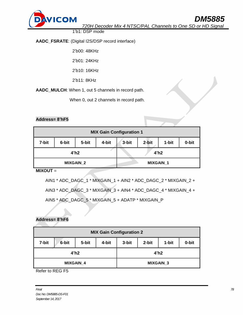
DM5885 720H Decoder Mix 4 NTSC/PAL Channels to One SD or HD Signal
Final 78
Doc No: DM5885-DS-F01
September 14, 2017
1’b1: DSP mode
AADC_FSRATE: (Digital I2S/DSP record interface)
2’b00: 48KHz
2’b01: 24KHz
2’b10: 16KHz
2’b11: 8KHz
AADC_MULCH: When 1, out 5 channels in record path.
When 0, out 2 channels in record path.
Address= 8’hF5
MIX Gain Configuration 1
7-bit 6-bit 5-bit 4-bit 3-bit 2-bit 1-bit 0-bit
4’h2 4’h2
MIXGAIN_2 MIXGAIN_1
MIXOUT =
AIN1 * ADC_DAGC_1 * MIXGAIN_1 + AIN2 * ADC_DAGC_2 * MIXGAIN_2 +
AIN3 * ADC_DAGC_3 * MIXGAIN_3 + AIN4 * ADC_DAGC_4 * MIXGAIN_4 +
AIN5 * ADC_DAGC_5 * MIXGAIN_5 + ADATP * MIXGAIN_P
Address= 8’hF6
MIX Gain Configuration 2
7-bit 6-bit 5-bit 4-bit 3-bit 2-bit 1-bit 0-bit
4’h2 4’h2
MIXGAIN_4 MIXGAIN_3
Refer to REG F5
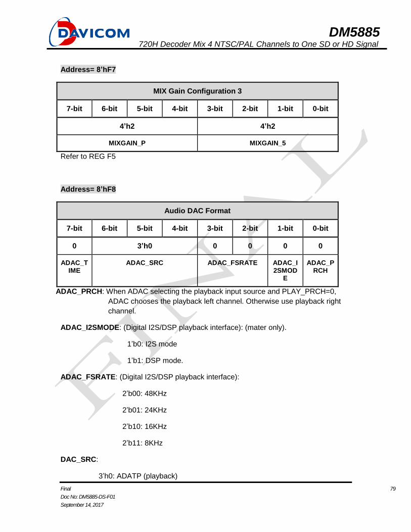
DM5885 720H Decoder Mix 4 NTSC/PAL Channels to One SD or HD Signal
Final 79
Doc No: DM5885-DS-F01
September 14, 2017
Address= 8’hF7
MIX Gain Configuration 3
7-bit 6-bit 5-bit 4-bit 3-bit 2-bit 1-bit 0-bit
4’h2 4’h2
MIXGAIN_P MIXGAIN_5
Refer to REG F5
Address= 8’hF8
Audio DAC Format
7-bit 6-bit 5-bit 4-bit 3-bit 2-bit 1-bit 0-bit
0 3’h0 0 0 0 0
ADAC_TIME
ADAC_SRC ADAC_FSRATE ADAC_I2SMOD
E
ADAC_PRCH
ADAC_PRCH: When ADAC selecting the playback input source and PLAY_PRCH=0,
ADAC chooses the playback left channel. Otherwise use playback right
channel.
ADAC_I2SMODE: (Digital I2S/DSP playback interface): (mater only).
1’b0: I2S mode
1’b1: DSP mode.
ADAC_FSRATE: (Digital I2S/DSP playback interface):
2’b00: 48KHz
2’b01: 24KHz
2’b10: 16KHz
2’b11: 8KHz
DAC_SRC:
3’h0: ADATP (playback)
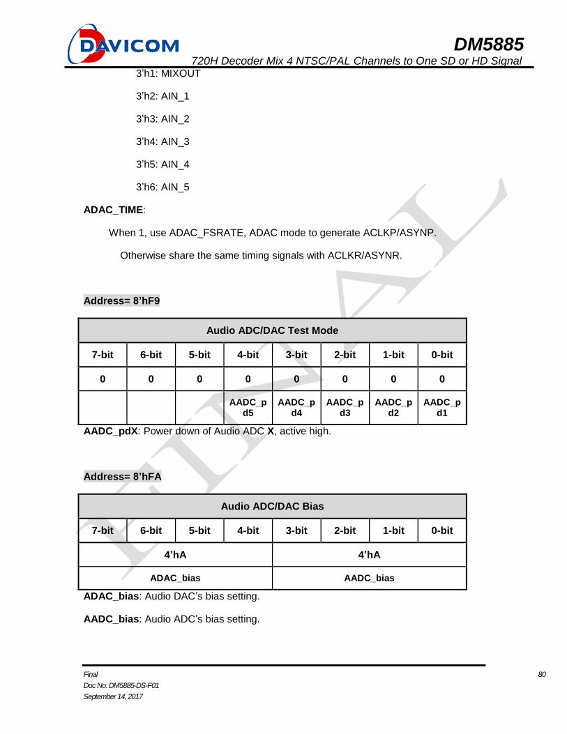
DM5885 720H Decoder Mix 4 NTSC/PAL Channels to One SD or HD Signal
Final 80
Doc No: DM5885-DS-F01
September 14, 2017
3’h1: MIXOUT
3’h2: AIN_1
3’h3: AIN_2
3’h4: AIN_3
3’h5: AIN_4
3’h6: AIN_5
ADAC_TIME:
When 1, use ADAC_FSRATE, ADAC mode to generate ACLKP/ASYNP.
Otherwise share the same timing signals with ACLKR/ASYNR.
Address= 8’hF9
Audio ADC/DAC Test Mode
7-bit 6-bit 5-bit 4-bit 3-bit 2-bit 1-bit 0-bit
0 0 0 0 0 0 0 0
AADC_pd5
AADC_pd4
AADC_pd3
AADC_pd2
AADC_pd1
AADC_pdX: Power down of Audio ADC X, active high.
Address= 8’hFA
Audio ADC/DAC Bias
7-bit 6-bit 5-bit 4-bit 3-bit 2-bit 1-bit 0-bit
4’hA 4’hA
ADAC_bias AADC_bias
ADAC_bias: Audio DAC’s bias setting.
AADC_bias: Audio ADC’s bias setting.
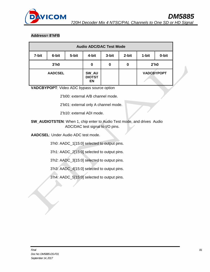
DM5885 720H Decoder Mix 4 NTSC/PAL Channels to One SD or HD Signal
Final 81
Doc No: DM5885-DS-F01
September 14, 2017
Address= 8’hFB
Audio ADC/DAC Test Mode
7-bit 6-bit 5-bit 4-bit 3-bit 2-bit 1-bit 0-bit
3’h0 0 0 0 2’h0
AADCSEL SW_AUDIOTST
EN
VADCBYPOPT
VADCBYPOPT: Video ADC bypass source option
2’b00: external A/B channel mode.
2’b01: external only A channel mode.
2’b10: external ADI mode.
SW_AUDIOTSTEN: When 1, chip enter to Audio Test mode, and drives Audio
ADC/DAC test signal to I/O pins.
AADCSEL: Under Audio ADC test mode.
3’h0: AADC_1[15:0] selected to output pins.
3’h1: AADC_2[15:0] selected to output pins.
3’h2: AADC_3[15:0] selected to output pins.
3’h3: AADC_4[15:0] selected to output pins.
3’h4: AADC_5[15:0] selected to output pins.
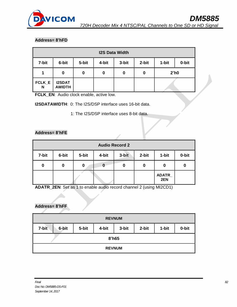
DM5885 720H Decoder Mix 4 NTSC/PAL Channels to One SD or HD Signal
Final 82
Doc No: DM5885-DS-F01
September 14, 2017
Address= 8’hFD
I2S Data Width
7-bit 6-bit 5-bit 4-bit 3-bit 2-bit 1-bit 0-bit
1 0 0 0 0 0 2’h0
FCLK_EN
I2SDATAWIDTH
FCLK_EN: Audio clock enable, active low.
I2SDATAWIDTH: 0: The I2S/DSP interface uses 16-bit data.
1: The I2S/DSP interface uses 8-bit data.
Address= 8’hFE
Audio Record 2
7-bit 6-bit 5-bit 4-bit 3-bit 2-bit 1-bit 0-bit
0 0 0 0 0 0 0 0
ADATR_2EN
ADATR_2EN: Set as 1 to enable audio record channel 2 (using MI2CD1)
Address= 8’hFF
REVNUM
7-bit 6-bit 5-bit 4-bit 3-bit 2-bit 1-bit 0-bit
8’h65
REVNUM
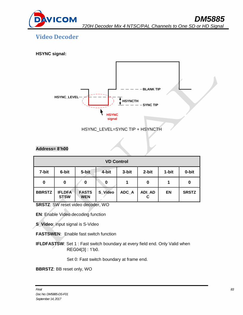
DM5885 720H Decoder Mix 4 NTSC/PAL Channels to One SD or HD Signal
Final 83
Doc No: DM5885-DS-F01
September 14, 2017
Video Decoder
HSYNC signal:
HSYNC
signal
BLANK TIP
SYNC TIP
HSYNC_LEVEL
HSYNCTH
HSYNC_LEVEL=SYNC TIP + HSYNCTH
Address= 8’h00
VD Control
7-bit 6-bit 5-bit 4-bit 3-bit 2-bit 1-bit 0-bit
0 0 0 0 1 0 1 0
BBRSTZ IFLDFASTSW
FASTSWEN
S_Video ADC_A ADI_ADC
EN SRSTZ
SRSTZ: SW reset video decoder, WO
EN: Enable Video decoding function
S_Video: input signal is S-Video
FASTSWEN: Enable fast switch function
IFLDFASTSW: Set 1 : Fast switch boundary at every field end. Only Valid when
REG04[3] : 1’b0.
Set 0: Fast switch boundary at frame end.
BBRSTZ: BB reset only, WO
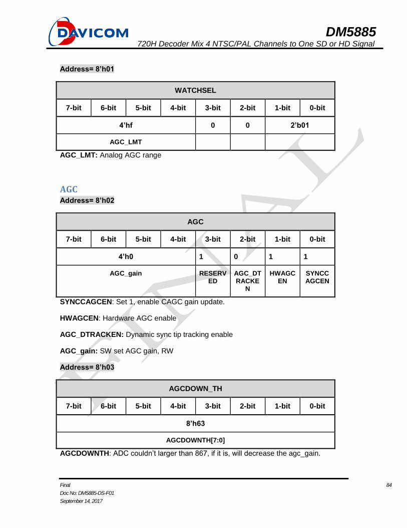
DM5885 720H Decoder Mix 4 NTSC/PAL Channels to One SD or HD Signal
Final 84
Doc No: DM5885-DS-F01
September 14, 2017
Address= 8’h01
WATCHSEL
7-bit 6-bit 5-bit 4-bit 3-bit 2-bit 1-bit 0-bit
4’hf 0 0 2’b01
AGC_LMT
AGC_LMT: Analog AGC range
AGC Address= 8’h02
AGC
7-bit 6-bit 5-bit 4-bit 3-bit 2-bit 1-bit 0-bit
4’h0 1 0 1 1
AGC_gain RESERVED
AGC_DTRACKE
N
HWAGCEN
SYNCCAGCEN
SYNCCAGCEN: Set 1, enable CAGC gain update.
HWAGCEN: Hardware AGC enable
AGC_DTRACKEN: Dynamic sync tip tracking enable
AGC_gain: SW set AGC gain, RW
Address= 8’h03
AGCDOWN_TH
7-bit 6-bit 5-bit 4-bit 3-bit 2-bit 1-bit 0-bit
8’h63
AGCDOWNTH[7:0]
AGCDOWNTH: ADC couldn’t larger than 867, if it is, will decrease the agc_gain.
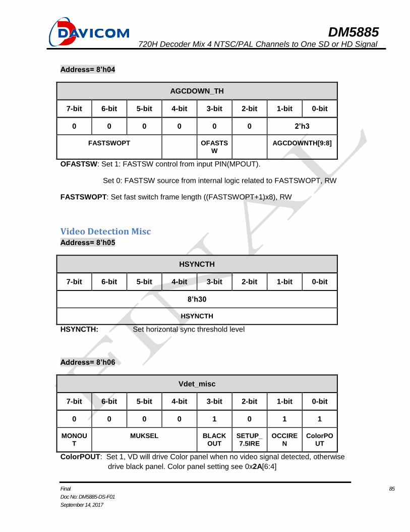
DM5885 720H Decoder Mix 4 NTSC/PAL Channels to One SD or HD Signal
Final 85
Doc No: DM5885-DS-F01
September 14, 2017
Address= 8’h04
AGCDOWN_TH
7-bit 6-bit 5-bit 4-bit 3-bit 2-bit 1-bit 0-bit
0 0 0 0 0 0 2’h3
FASTSWOPT OFASTSW
AGCDOWNTH[9:8]
OFASTSW: Set 1: FASTSW control from input PIN(MPOUT).
Set 0: FASTSW source from internal logic related to FASTSWOPT, RW
FASTSWOPT: Set fast switch frame length ((FASTSWOPT+1)x8), RW
Video Detection Misc Address= 8’h05
HSYNCTH
7-bit 6-bit 5-bit 4-bit 3-bit 2-bit 1-bit 0-bit
8’h30
HSYNCTH
HSYNCTH: Set horizontal sync threshold level
Address= 8’h06
Vdet_misc
7-bit 6-bit 5-bit 4-bit 3-bit 2-bit 1-bit 0-bit
0 0 0 0 1 0 1 1
MONOUT
MUKSEL BLACKOUT
SETUP_7.5IRE
OCCIREN
ColorPOUT
ColorPOUT: Set 1, VD will drive Color panel when no video signal detected, otherwise
drive black panel. Color panel setting see 0x2A[6:4]
DM5885 720H Decoder Mix 4 NTSC/PAL Channels to One SD or HD Signal
Final 86
Doc No: DM5885-DS-F01
September 14, 2017
OCCIREN: Set 1, VD will out CCIR656
SETUP_7.5IRE: Set 1, add 7.5 IRE to the BLANK_TIP
BLACKOUT: Set 1, VD will drive black panel or blue panel when no video signal
detected.
MONOUT: force CCIR656 Cb=128, Cr=128
Color Killer Address= 8’h08
ColorKill TH
7-bit 6-bit 5-bit 4-bit 3-bit 2-bit 1-bit 0-bit
8’h20
CBDIFFTH[7:0]
CBDIFFTH: Set the color burst difference threshold
2D Comb Filter Address= 8’h09
Com2D_CFG
7-bit 6-bit 5-bit 4-bit 3-bit 2-bit 1-bit 0-bit
0 0 0 0 0 0 0 0
FORCE_MONO
FORCE_VCOMB
NOTCHFLTSEL
DIS_VCOMB
DIS_VCOMB: Set 1 to disable vertical comb filter
NOTCHFLTSEL: Set 0, use the wide band notch filter
Set 1, use the narrow band notch filter
FORCE_MONO: Set 1 to force the MONO signal mode.
DM5885 720H Decoder Mix 4 NTSC/PAL Channels to One SD or HD Signal
Final 87
Doc No: DM5885-DS-F01
September 14, 2017
Address= 8’h0C
PAL SW CFG
7-bit 6-bit 5-bit 4-bit 3-bit 2-bit 1-bit 0-bit
2’h0 5’h1 0
Y_SHARP_GAIN RESERVED PALSWOPT
PALSWOPT: Set 1 to use standard pal switch define to demodulation.
For line lock camera, set this bit to 1.
Y_SHARP_GAIN:
2’h0 : no sharpness function
2’h1: sharpness gain 0.5
2’h2: sharpness gain 1
2’h3: sharpness gain 2
Address= 8’h10
VD Decoder status
7-bit 6-bit 5-bit 4-bit 3-bit 2-bit 1-bit 0-bit
0 0 0 0 0 0 0 0
PAL_Nc PAL-I,B,B1,G
,H,D/ PAL_N
PAL_M
PAL_60 NTSC-443
NTSC-J/NTSC-
M
COLOR KILL_52
5
COLORKILL_62
5
The register show the video decoded status
RO. Set 1 to enable SW force mode.

DM5885 720H Decoder Mix 4 NTSC/PAL Channels to One SD or HD Signal
Final 88
Doc No: DM5885-DS-F01
September 14, 2017
Address= 8’h11
VD_STS
7-bit 6-bit 5-bit 4-bit 3-bit 2-bit 1-bit 0-bit
0 0 0 0 0 0 0 0
CLKLOCK_STS
T
DET_NONILT
DET_NONILT: RO. Detect the non-interlaced signal format.
CLKLOCK_STST: RO. Clock offset lock status
Address= 8’h12
DAGC_LMT
7-bit 6-bit 5-bit 4-bit 3-bit 2-bit 1-bit 0-bit
4’h3 4’hf
CLKOFF_LOCK DAGC_LMT
DAGC_LMT: Digital AGC range
CLKOFF_LOCK: Clock offset locking function. 4’h0: always tracking
Others: clock offset lock within CLKOFF_LOCK * 8 ppm.
Address= 8’h13
VD_CFG
7-bit 6-bit 5-bit 4-bit 3-bit 2-bit 1-bit 0-bit
0 1 1 0 1 0 1 1
SWFAR54MD
HWFAR54OPT
GAINLOCK_OPT
CLKOFFDIS
CBADJ BLANK_SHIFTE
N
ALINELOCK
CLKOFF_TRACK
EN
CLKOFF_TRACKEN: CLKOFFSET tracking enable
DM5885 720H Decoder Mix 4 NTSC/PAL Channels to One SD or HD Signal
Final 89
Doc No: DM5885-DS-F01
September 14, 2017
ALINELOCK: active line lock option, fixed line start position.
BLANK_SHIFTEN: set 1, blank level will be modified according to color burst mean
value per line.
CBADJ: Color burst adjust
CLKOFFDIS: Disable clock offset tracking function
GAINLOCK_OPT: Enable gain locking function after 16 frame decoded.
HWFAR54OPT: Set 1, FAR4FS will operate in 54Mhz when detecting 4.43 subcarrier
SWFAR54MD: Software force FAR4FS operate in 54Mhz.
Address= 8’h14
VD_CFG
7-bit 6-bit 5-bit 4-bit 3-bit 2-bit 1-bit 0-bit
0 0 0 1 0 1 0 1
LLCFASTMD VDETOPT
LTRACKOPT
CLKLOCKOPT
CLKLOCKOPT: Set 0 : Always tracking clock offset when
abs(clkoffset)> CLKOFF_LOCK (REG12[7:4])
Set 1 : keep tracking until first time
abs(clkoffset)< CLKOFF_LOCK(REG12[7:4])
LTRACKOPT: Set 1: Hardware continues active line (video) decoding when miss
valid HSYNC signal until video loss.
Set 0: Hardware performs active line (video) decoding until valid
HSYNC signal detected.
VDETOPT: Set 1: using rising edge of HSYNC signal as line detection timing.
Set0: using falling edge of HSYNC signal as line detection timing.
For long cable application, set this bit to 1.
LLCFASTMD[1:0]:
Line lock Auto Detection stable period. Valid when REG3B[5]=1.
DM5885 720H Decoder Mix 4 NTSC/PAL Channels to One SD or HD Signal
Final 90
Doc No: DM5885-DS-F01
September 14, 2017
Set 0: check line lock mode right after decode started
Set 1: check line lock mode after 8 frames decoded.
Set 2, 3: check line lock mode after 16 frames decoded.
Address= 8’h15
CLKOFF_CTL
7-bit 6-bit 5-bit 4-bit 3-bit 2-bit 1-bit 0-bit
0 0 0 0 1 1 0 0
RESERVED
CLKFRACEN
FIXHSYNC_MD
L
SWFIXCLOCKO
FF
SWFIXCLOCKOFF: Set 1, SW fixed clock offset. Force clock offset value=
{REG25[4:0],REG24[7:0],REG23[7:0]}.
FIXHSYNC_MDL: Set 1, fixed the HSYNC_LEVEL to be REG05 HSYNCTH.
CLKFRACEN: Set 1, enable fraction clock offset tracking.
Address= 8’h17
CTI gain
7-bit 6-bit 5-bit 4-bit 3-bit 2-bit 1-bit 0-bit
0 0 6’d10
HMIDTRACK
HMIDTRACK: Set 1: tracking BLANK TIP each line at Front Porch Blanking position
(REG4B[7:0]).
Set 0: tracking BLANK TIP at CVBS serration period.
Note: 6’d10, d=decimal
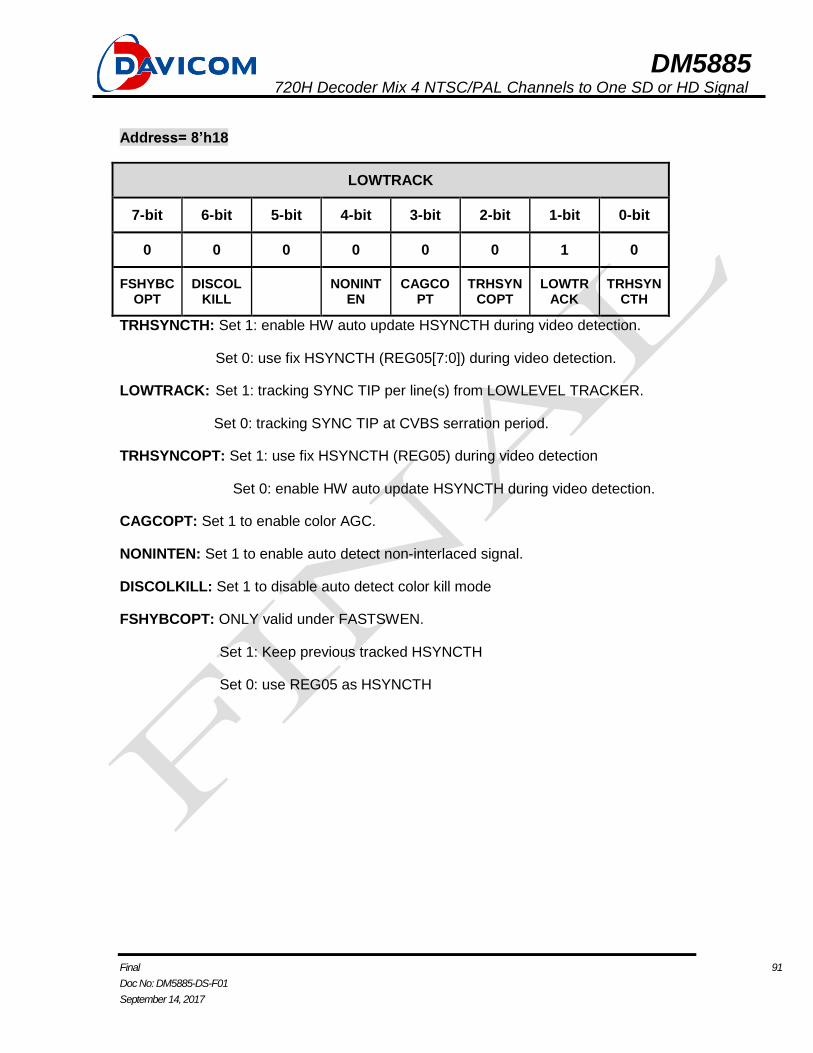
DM5885 720H Decoder Mix 4 NTSC/PAL Channels to One SD or HD Signal
Final 91
Doc No: DM5885-DS-F01
September 14, 2017
Address= 8’h18
LOWTRACK
7-bit 6-bit 5-bit 4-bit 3-bit 2-bit 1-bit 0-bit
0 0 0 0 0 0 1 0
FSHYBCOPT
DISCOLKILL
NONINTEN
CAGCOPT
TRHSYNCOPT
LOWTRACK
TRHSYNCTH
TRHSYNCTH: Set 1: enable HW auto update HSYNCTH during video detection.
Set 0: use fix HSYNCTH (REG05[7:0]) during video detection.
LOWTRACK: Set 1: tracking SYNC TIP per line(s) from LOWLEVEL TRACKER.
Set 0: tracking SYNC TIP at CVBS serration period.
TRHSYNCOPT: Set 1: use fix HSYNCTH (REG05) during video detection
Set 0: enable HW auto update HSYNCTH during video detection.
CAGCOPT: Set 1 to enable color AGC.
NONINTEN: Set 1 to enable auto detect non-interlaced signal.
DISCOLKILL: Set 1 to disable auto detect color kill mode
FSHYBCOPT: ONLY valid under FASTSWEN.
Set 1: Keep previous tracked HSYNCTH
Set 0: use REG05 as HSYNCTH
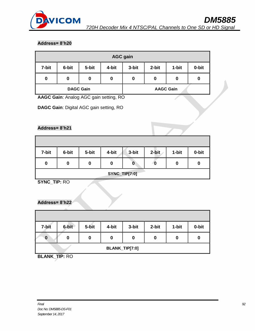
DM5885 720H Decoder Mix 4 NTSC/PAL Channels to One SD or HD Signal
Final 92
Doc No: DM5885-DS-F01
September 14, 2017
Address= 8’h20
AGC gain
7-bit 6-bit 5-bit 4-bit 3-bit 2-bit 1-bit 0-bit
0 0 0 0 0 0 0 0
DAGC Gain AAGC Gain
AAGC Gain: Analog AGC gain setting, RO
DAGC Gain: Digital AGC gain setting, RO
Address= 8’h21
7-bit 6-bit 5-bit 4-bit 3-bit 2-bit 1-bit 0-bit
0 0 0 0 0 0 0 0
SYNC_TIP[7:0]
SYNC_TIP: RO
Address= 8’h22
7-bit 6-bit 5-bit 4-bit 3-bit 2-bit 1-bit 0-bit
0 0 0 0 0 0 0 0
BLANK_TIP[7:0]
BLANK_TIP: RO
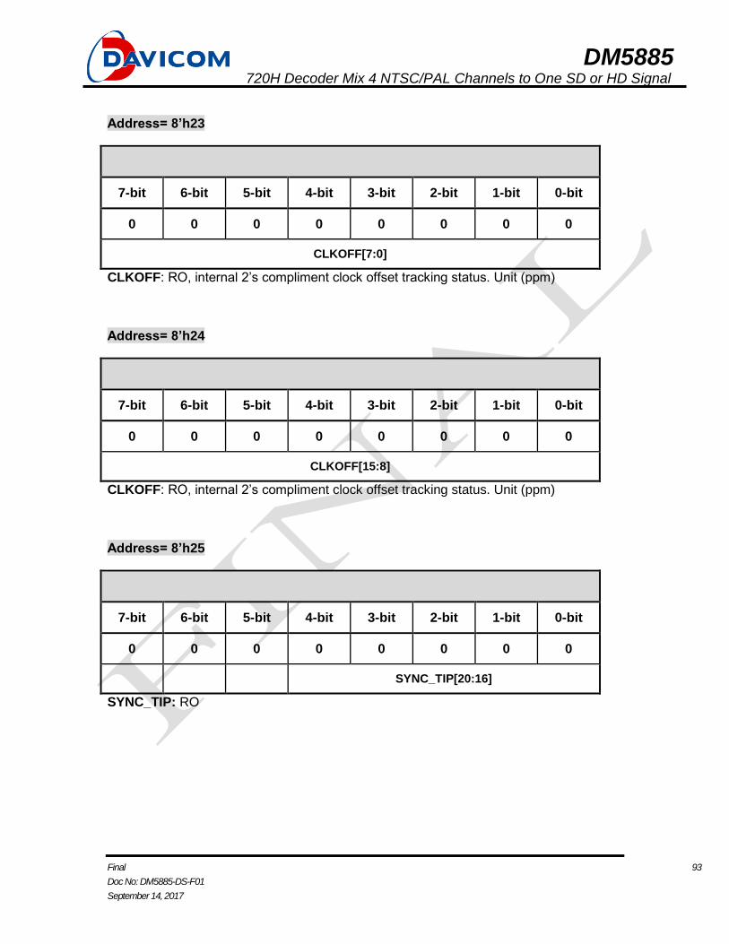
DM5885 720H Decoder Mix 4 NTSC/PAL Channels to One SD or HD Signal
Final 93
Doc No: DM5885-DS-F01
September 14, 2017
Address= 8’h23
7-bit 6-bit 5-bit 4-bit 3-bit 2-bit 1-bit 0-bit
0 0 0 0 0 0 0 0
CLKOFF[7:0]
CLKOFF: RO, internal 2’s compliment clock offset tracking status. Unit (ppm)
Address= 8’h24
7-bit 6-bit 5-bit 4-bit 3-bit 2-bit 1-bit 0-bit
0 0 0 0 0 0 0 0
CLKOFF[15:8]
CLKOFF: RO, internal 2’s compliment clock offset tracking status. Unit (ppm)
Address= 8’h25
7-bit 6-bit 5-bit 4-bit 3-bit 2-bit 1-bit 0-bit
0 0 0 0 0 0 0 0
SYNC_TIP[20:16]
SYNC_TIP: RO
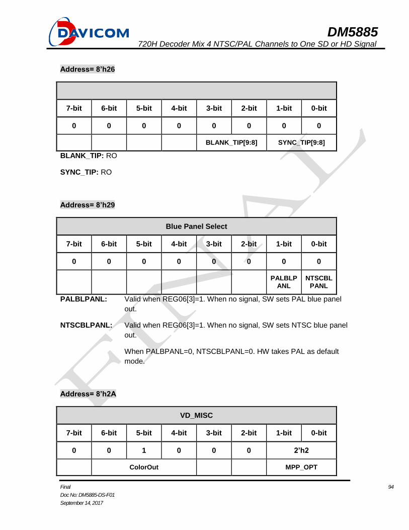
DM5885 720H Decoder Mix 4 NTSC/PAL Channels to One SD or HD Signal
Final 94
Doc No: DM5885-DS-F01
September 14, 2017
Address= 8’h26
7-bit 6-bit 5-bit 4-bit 3-bit 2-bit 1-bit 0-bit
0 0 0 0 0 0 0 0
BLANK_TIP[9:8] SYNC_TIP[9:8]
BLANK_TIP: RO
SYNC_TIP: RO
Address= 8’h29
Blue Panel Select
7-bit 6-bit 5-bit 4-bit 3-bit 2-bit 1-bit 0-bit
0 0 0 0 0 0 0 0
PALBLPANL
NTSCBLPANL
PALBLPANL: Valid when REG06[3]=1. When no signal, SW sets PAL blue panel
out.
NTSCBLPANL: Valid when REG06[3]=1. When no signal, SW sets NTSC blue panel
out.
When PALBPANL=0, NTSCBLPANL=0. HW takes PAL as default
mode.
Address= 8’h2A
VD_MISC
7-bit 6-bit 5-bit 4-bit 3-bit 2-bit 1-bit 0-bit
0 0 1 0 0 0 2’h2
ColorOut MPP_OPT
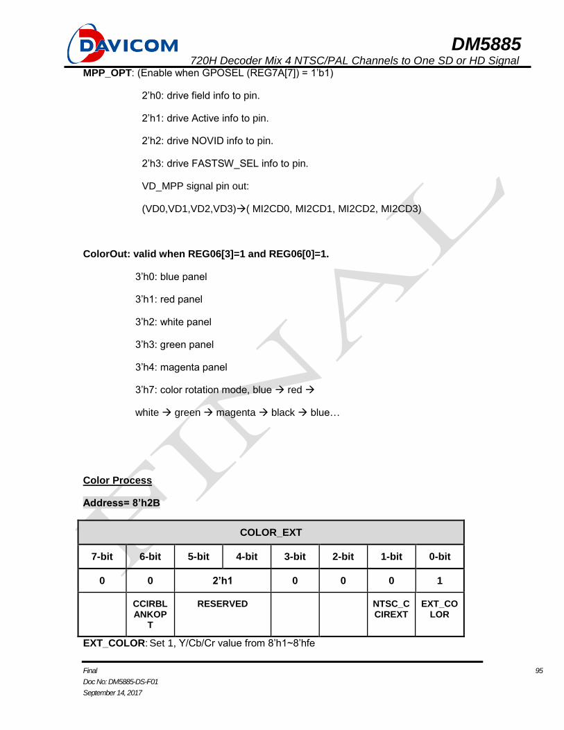
DM5885 720H Decoder Mix 4 NTSC/PAL Channels to One SD or HD Signal
Final 95
Doc No: DM5885-DS-F01
September 14, 2017
MPP_OPT: (Enable when GPOSEL (REG7A[7]) = 1’b1)
2’h0: drive field info to pin.
2’h1: drive Active info to pin.
2’h2: drive NOVID info to pin.
2’h3: drive FASTSW_SEL info to pin.
VD_MPP signal pin out:
(VD0,VD1,VD2,VD3)( MI2CD0, MI2CD1, MI2CD2, MI2CD3)
ColorOut: valid when REG06[3]=1 and REG06[0]=1.
3’h0: blue panel
3’h1: red panel
3’h2: white panel
3’h3: green panel
3’h4: magenta panel
3’h7: color rotation mode, blue red
white green magenta black blue…
Color Process
Address= 8’h2B
COLOR_EXT
7-bit 6-bit 5-bit 4-bit 3-bit 2-bit 1-bit 0-bit
0 0 2’h1 0 0 0 1
CCIRBLANKOP
T
RESERVED NTSC_CCIREXT
EXT_COLOR
EXT_COLOR: Set 1, Y/Cb/Cr value from 8’h1~8’hfe
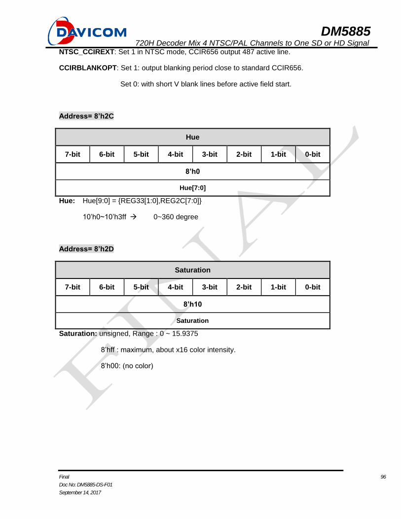
DM5885 720H Decoder Mix 4 NTSC/PAL Channels to One SD or HD Signal
Final 96
Doc No: DM5885-DS-F01
September 14, 2017
NTSC_CCIREXT: Set 1 in NTSC mode, CCIR656 output 487 active line.
CCIRBLANKOPT: Set 1: output blanking period close to standard CCIR656.
Set 0: with short V blank lines before active field start.
Address= 8’h2C
Hue
7-bit 6-bit 5-bit 4-bit 3-bit 2-bit 1-bit 0-bit
8’h0
Hue[7:0]
Hue: Hue[9:0] = {REG33[1:0],REG2C[7:0]}
10’h0~10’h3ff 0~360 degree
Address= 8’h2D
Saturation
7-bit 6-bit 5-bit 4-bit 3-bit 2-bit 1-bit 0-bit
8’h10
Saturation
Saturation: unsigned, Range : 0 ~ 15.9375
8’hff : maximum, about x16 color intensity.
8’h00: (no color)
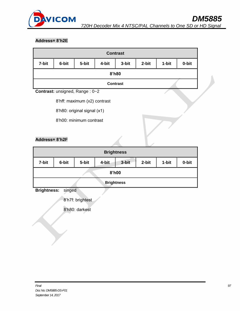
DM5885 720H Decoder Mix 4 NTSC/PAL Channels to One SD or HD Signal
Final 97
Doc No: DM5885-DS-F01
September 14, 2017
Address= 8’h2E
Contrast
7-bit 6-bit 5-bit 4-bit 3-bit 2-bit 1-bit 0-bit
8’h80
Contrast
Contrast: unsigned, Range : 0~2
8’hff: maximum (x2) contrast
8’h80: original signal (x1)
8’h00: minimum contrast
Address= 8’h2F
Brightness
7-bit 6-bit 5-bit 4-bit 3-bit 2-bit 1-bit 0-bit
8’h00
Brightness
Brightness: singed
8’h7f: brightest
8’h80: darkest
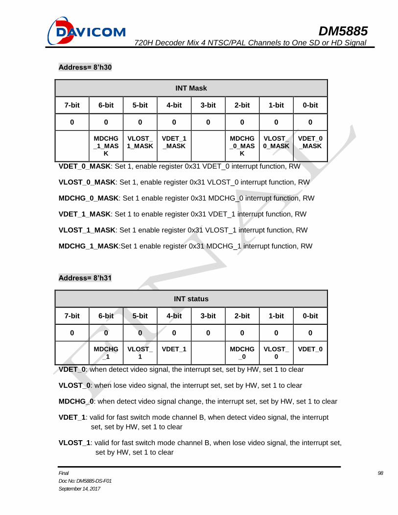
DM5885 720H Decoder Mix 4 NTSC/PAL Channels to One SD or HD Signal
Final 98
Doc No: DM5885-DS-F01
September 14, 2017
Address= 8’h30
INT Mask
7-bit 6-bit 5-bit 4-bit 3-bit 2-bit 1-bit 0-bit
0 0 0 0 0 0 0 0
MDCHG_1_MAS
K
VLOST_1_MASK
VDET_1_MASK
MDCHG_0_MAS
K
VLOST_0_MASK
VDET_0_MASK
VDET_0_MASK: Set 1, enable register 0x31 VDET_0 interrupt function, RW
VLOST_0_MASK: Set 1, enable register 0x31 VLOST_0 interrupt function, RW
MDCHG_0_MASK: Set 1 enable register 0x31 MDCHG_0 interrupt function, RW
VDET_1_MASK: Set 1 to enable register 0x31 VDET_1 interrupt function, RW
VLOST_1_MASK: Set 1 enable register 0x31 VLOST_1 interrupt function, RW
MDCHG_1_MASK:Set 1 enable register 0x31 MDCHG_1 interrupt function, RW
Address= 8’h31
INT status
7-bit 6-bit 5-bit 4-bit 3-bit 2-bit 1-bit 0-bit
0 0 0 0 0 0 0 0
MDCHG_1
VLOST_1
VDET_1 MDCHG_0
VLOST_0
VDET_0
VDET_0: when detect video signal, the interrupt set, set by HW, set 1 to clear
VLOST_0: when lose video signal, the interrupt set, set by HW, set 1 to clear
MDCHG_0: when detect video signal change, the interrupt set, set by HW, set 1 to clear
VDET_1: valid for fast switch mode channel B, when detect video signal, the interrupt
set, set by HW, set 1 to clear
VLOST_1: valid for fast switch mode channel B, when lose video signal, the interrupt set,
set by HW, set 1 to clear
DM5885 720H Decoder Mix 4 NTSC/PAL Channels to One SD or HD Signal
Final 99
Doc No: DM5885-DS-F01
September 14, 2017
MDCHG_1: valid for fast switch mode channel B, when detect video signal change
format, the interrupt set, set by HW, set 1 to clear
Address= 8’h33
HUE
7-bit 6-bit 5-bit 4-bit 3-bit 2-bit 1-bit 0-bit
0 0 0 0 0 0 0 0
Hue[9:8]
Hue: Hue[9:0] = {REG33[1:0],REG2C[7:0]}
10’h0~10’h3ff 0~360 degree
Address= 8’h34
FIELD OPTION
7-bit 6-bit 5-bit 4-bit 3-bit 2-bit 1-bit 0-bit
0 0 0 0 0 0 0 0
FIELD_INV
FIELD_ONLY
FIELD_ONLY: CCIR656 signal output field 0 only
FILED_INV: Inverse output CCIR656 signal field
Address= 8’h35
Chroma Average
7-bit 6-bit 5-bit 4-bit 3-bit 2-bit 1-bit 0-bit
0 0 0 0 0 0 0 1
CAVNTSCMD
CAVPALMD
CAVNTSCMD: Set 1, enable NTSC mode Cb/Cr line average.
DM5885 720H Decoder Mix 4 NTSC/PAL Channels to One SD or HD Signal
Final 100
Doc No: DM5885-DS-F01
September 14, 2017
Set 0, disable.
CAVPALMD: Set 1, enable PAL mode Cb/Cr line average.
Set 0, disable.
Address= 8’h36
MASK CCIR656 LINE
7-bit 6-bit 5-bit 4-bit 3-bit 2-bit 1-bit 0-bit
0 0 0 0 0 0 0 0
MASKALL
PAL_MSK3
PAL_MSK3: Set 1, it will mask field 0 and 1 last lines according to REG37
MASKALL: mask all active
Address= 8’h37
MASK LINE
7-bit 6-bit 5-bit 4-bit 3-bit 2-bit 1-bit 0-bit
0 3’h0 0 3’h0
MSK_LINE_F1 MSK_LINE_F0
MSK_LINE_F0: When REG36[0] = 1, Mask Field 0 last number of active lines (0-7)
MSK_LINE_F1: When REG36[0] = 1, Mask Field 1 last number of active lines (0-7)
DM5885 720H Decoder Mix 4 NTSC/PAL Channels to One SD or HD Signal
Final 101
Doc No: DM5885-DS-F01
September 14, 2017
Address= 8’h38
MONO TH
7-bit 6-bit 5-bit 4-bit 3-bit 2-bit 1-bit 0-bit
1 0 0 5’d31
MONO_EN
MONO_TH
MONO_TH: MONO mode AGC threshold. AGC max value 30. when set MONO_TH 31.
AGC will always less than MONO_TH.
MONO_EN: Set 0, when no valid color burst detected.
Output CCIR656 Y through Notch filter.
Set 1, when no valid color burst detected. Output CCIR656
Y through Notch filer if AGC_GAIN>=MONO_TH, otherwise output
CCIR656 Y with ADC data.
When No valid color burst detected (color kill mode). Output
CCIR656 Cb/Cr with 128 (no color).
Note: 5’d31, d=decimal
Address= 8’h39
COLOR BURST DETECT
7-bit 6-bit 5-bit 4-bit 3-bit 2-bit 1-bit 0-bit
0 3’h4 4’h5
COLBSTCYC COLBSTHSEL
COLBSTHSEL:Color Burst detection threshold.
4’h0:COLBSTH = 0.125*(BLANK TIP – SYNC TIP)
DM5885 720H Decoder Mix 4 NTSC/PAL Channels to One SD or HD Signal
Final 102
Doc No: DM5885-DS-F01
September 14, 2017
4’h1:COLBSTH = 0.25*(BLANK TIP – SYNC TIP)
4’h2:COLBSTH = 0.375*(BLANK TIP – SYNC TIP)
4’h3:COLBSTH = 0.5*(BLANK TIP – SYNC TIP)
4’h4:COLBSTH = 0.09375*(BLANK TIP – SYNC TIP)
4’h5:COLBSTH = 0.078125*(BLANK TIP – SYNC TIP)
4’h6:COLBSTH = 0.0625*(BLANK TIP – SYNC TIP)
4’h7:COLBSTH = 0.03125*(BLANK TIP – SYNC TIP)
4’h8:COLBSTH = 0
When color burst peak to peak value larger than COLBSTHSEL, it’s
been considered a good color burst signal cycle.
COLBSTCYC: When COLBSTCYC numbers of valid color bust cycle detected, VD
will decode video with color and Color AGC will optionally started.
Otherwise will enter color kill mode.
Address= 8’h3A
CAGC
7-bit 6-bit 5-bit 4-bit 3-bit 2-bit 1-bit 0-bit
1 0 0 0 0 1 0 0
CAGCEN
CAGCLOCKOP
cagc_gain
cagc_gain: RO. Chroma gain value. [5:2] integer, [1:0] fractional.
(max 15.75, min 1)
CAGCLOCKOPT: Set 1, enable color AGC tracking until CAGC gain stable.
Set 0, color AGC tracking for first 15 video decoded frames.
CAGCEN : Set 1, enable color AGC.
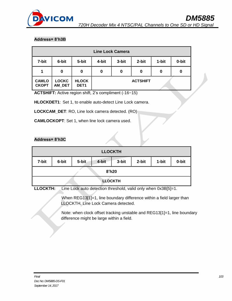
DM5885 720H Decoder Mix 4 NTSC/PAL Channels to One SD or HD Signal
Final 103
Doc No: DM5885-DS-F01
September 14, 2017
Address= 8’h3B
Line Lock Camera
7-bit 6-bit 5-bit 4-bit 3-bit 2-bit 1-bit 0-bit
1 0 0 0 0 0 0 0
CAMLOCKOPT
LOCKCAM_DET
HLOCKDET1
ACTSHIFT
ACTSHIFT: Active region shift, 2’s compliment (-16~15)
HLOCKDET1: Set 1, to enable auto-detect Line Lock camera.
LOCKCAM_DET: RO, Line lock camera detected. (RO)
CAMLOCKOPT: Set 1, when line lock camera used.
Address= 8’h3C
LLOCKTH
7-bit 6-bit 5-bit 4-bit 3-bit 2-bit 1-bit 0-bit
8’h20
LLOCKTH
LLOCKTH: Line Lock auto detection threshold, valid only when 0x3B[5]=1.
When REG13[1]=1, line boundary difference within a field larger than
LLOCKTH, Line Lock Camera detected.
Note: when clock offset tracking unstable and REG13[1]=1, line boundary
difference might be large within a field.
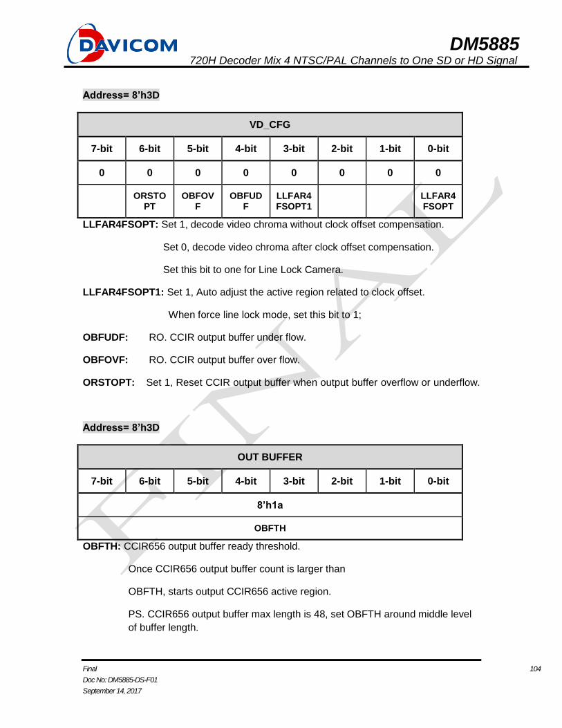
DM5885 720H Decoder Mix 4 NTSC/PAL Channels to One SD or HD Signal
Final 104
Doc No: DM5885-DS-F01
September 14, 2017
Address= 8’h3D
VD_CFG
7-bit 6-bit 5-bit 4-bit 3-bit 2-bit 1-bit 0-bit
0 0 0 0 0 0 0 0
ORSTOPT
OBFOVF
OBFUDF
LLFAR4FSOPT1
LLFAR4FSOPT
LLFAR4FSOPT: Set 1, decode video chroma without clock offset compensation.
Set 0, decode video chroma after clock offset compensation.
Set this bit to one for Line Lock Camera.
LLFAR4FSOPT1: Set 1, Auto adjust the active region related to clock offset.
When force line lock mode, set this bit to 1;
OBFUDF: RO. CCIR output buffer under flow.
OBFOVF: RO. CCIR output buffer over flow.
ORSTOPT: Set 1, Reset CCIR output buffer when output buffer overflow or underflow.
Address= 8’h3D
OUT BUFFER
7-bit 6-bit 5-bit 4-bit 3-bit 2-bit 1-bit 0-bit
8’h1a
OBFTH
OBFTH: CCIR656 output buffer ready threshold.
Once CCIR656 output buffer count is larger than
OBFTH, starts output CCIR656 active region.
PS. CCIR656 output buffer max length is 48, set OBFTH around middle level
of buffer length.
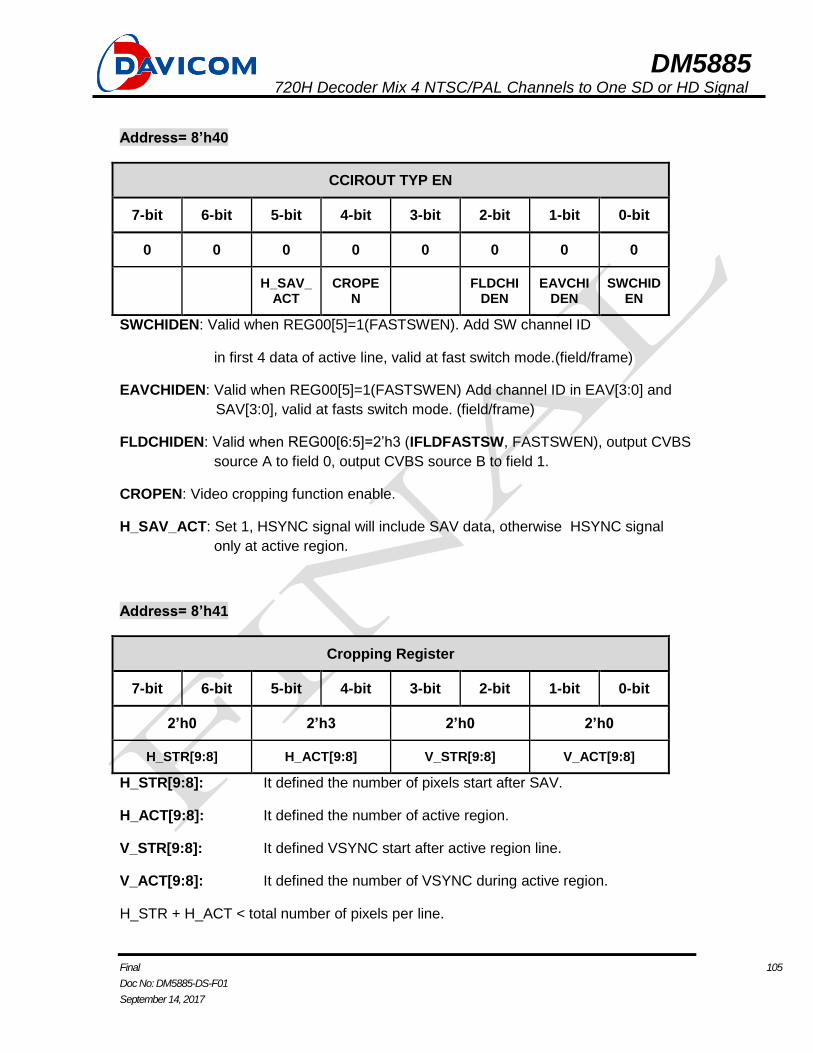
DM5885 720H Decoder Mix 4 NTSC/PAL Channels to One SD or HD Signal
Final 105
Doc No: DM5885-DS-F01
September 14, 2017
Address= 8’h40
CCIROUT TYP EN
7-bit 6-bit 5-bit 4-bit 3-bit 2-bit 1-bit 0-bit
0 0 0 0 0 0 0 0
H_SAV_ACT
CROPEN
FLDCHIDEN
EAVCHIDEN
SWCHIDEN
SWCHIDEN: Valid when REG00[5]=1(FASTSWEN). Add SW channel ID
in first 4 data of active line, valid at fast switch mode.(field/frame)
EAVCHIDEN: Valid when REG00[5]=1(FASTSWEN) Add channel ID in EAV[3:0] and
SAV[3:0], valid at fasts switch mode. (field/frame)
FLDCHIDEN: Valid when REG00[6:5]=2’h3 (IFLDFASTSW, FASTSWEN), output CVBS
source A to field 0, output CVBS source B to field 1.
CROPEN: Video cropping function enable.
H_SAV_ACT: Set 1, HSYNC signal will include SAV data, otherwise HSYNC signal
only at active region.
Address= 8’h41
Cropping Register
7-bit 6-bit 5-bit 4-bit 3-bit 2-bit 1-bit 0-bit
2’h0 2’h3 2’h0 2’h0
H_STR[9:8] H_ACT[9:8] V_STR[9:8] V_ACT[9:8]
H_STR[9:8]: It defined the number of pixels start after SAV.
H_ACT[9:8]: It defined the number of active region.
V_STR[9:8]: It defined VSYNC start after active region line.
V_ACT[9:8]: It defined the number of VSYNC during active region.
H_STR + H_ACT < total number of pixels per line.
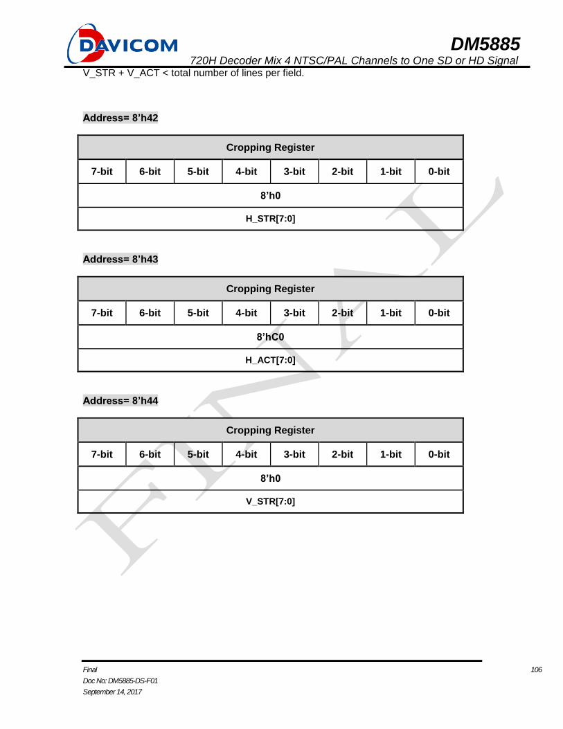
DM5885 720H Decoder Mix 4 NTSC/PAL Channels to One SD or HD Signal
Final 106
Doc No: DM5885-DS-F01
September 14, 2017
V_STR + V_ACT < total number of lines per field.
Address= 8’h42
Cropping Register
7-bit 6-bit 5-bit 4-bit 3-bit 2-bit 1-bit 0-bit
8’h0
H_STR[7:0]
Address= 8’h43
Cropping Register
7-bit 6-bit 5-bit 4-bit 3-bit 2-bit 1-bit 0-bit
8’hC0
H_ACT[7:0]
Address= 8’h44
Cropping Register
7-bit 6-bit 5-bit 4-bit 3-bit 2-bit 1-bit 0-bit
8’h0
V_STR[7:0]
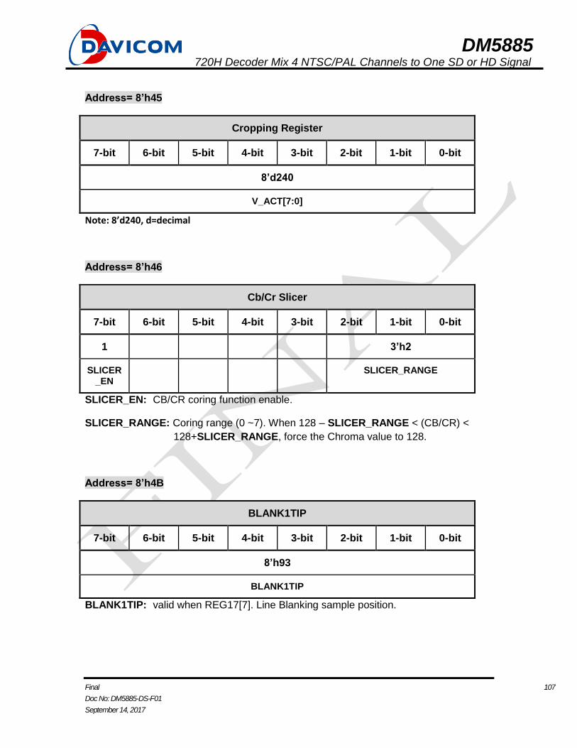
DM5885 720H Decoder Mix 4 NTSC/PAL Channels to One SD or HD Signal
Final 107
Doc No: DM5885-DS-F01
September 14, 2017
Address= 8’h45
Cropping Register
7-bit 6-bit 5-bit 4-bit 3-bit 2-bit 1-bit 0-bit
8’d240
V_ACT[7:0]
Note: 8’d240, d=decimal
Address= 8’h46
Cb/Cr Slicer
7-bit 6-bit 5-bit 4-bit 3-bit 2-bit 1-bit 0-bit
1 3’h2
SLICER_EN
SLICER_RANGE
SLICER_EN: CB/CR coring function enable.
SLICER_RANGE: Coring range (0 ~7). When 128 – SLICER_RANGE < (CB/CR) <
128+SLICER_RANGE, force the Chroma value to 128.
Address= 8’h4B
BLANK1TIP
7-bit 6-bit 5-bit 4-bit 3-bit 2-bit 1-bit 0-bit
8’h93
BLANK1TIP
BLANK1TIP: valid when REG17[7]. Line Blanking sample position.
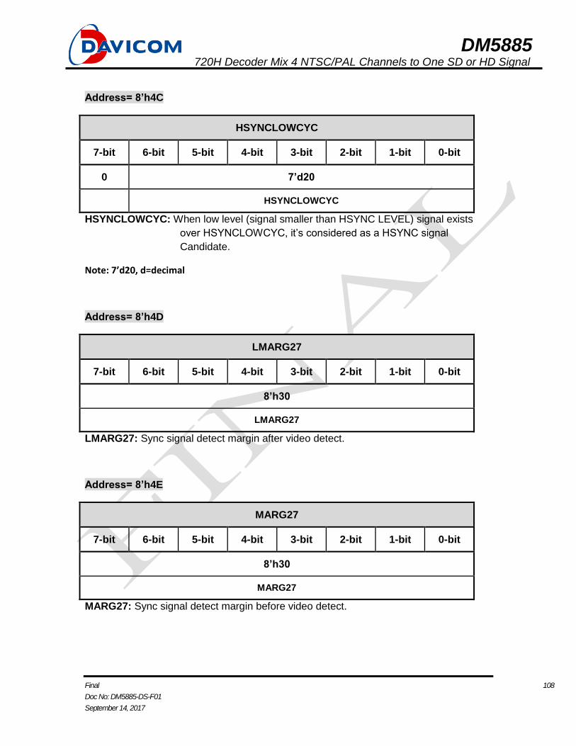
DM5885 720H Decoder Mix 4 NTSC/PAL Channels to One SD or HD Signal
Final 108
Doc No: DM5885-DS-F01
September 14, 2017
Address= 8’h4C
HSYNCLOWCYC
7-bit 6-bit 5-bit 4-bit 3-bit 2-bit 1-bit 0-bit
0 7’d20
HSYNCLOWCYC
HSYNCLOWCYC: When low level (signal smaller than HSYNC LEVEL) signal exists
over HSYNCLOWCYC, it’s considered as a HSYNC signal
Candidate.
Note: 7’d20, d=decimal
Address= 8’h4D
LMARG27
7-bit 6-bit 5-bit 4-bit 3-bit 2-bit 1-bit 0-bit
8’h30
LMARG27
LMARG27: Sync signal detect margin after video detect.
Address= 8’h4E
MARG27
7-bit 6-bit 5-bit 4-bit 3-bit 2-bit 1-bit 0-bit
8’h30
MARG27
MARG27: Sync signal detect margin before video detect.
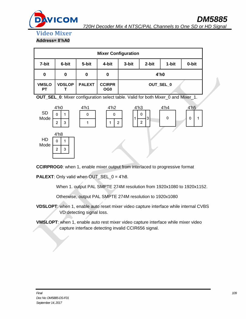
DM5885 720H Decoder Mix 4 NTSC/PAL Channels to One SD or HD Signal
Final 109
Doc No: DM5885-DS-F01
September 14, 2017
Video Mixer Address= 8’hA0
Mixer Configuration
7-bit 6-bit 5-bit 4-bit 3-bit 2-bit 1-bit 0-bit
0 0 0 0 4’h0
VMSLOPT
VDSLOPT
PALEXT CCIRPROG0
OUT_SEL_0
OUT_SEL_0: Mixer configuration select table. Valid for both Mixer_0 and Mixer_1.
0 1
2 3
0
1
0
1 2
0 0 110
23
SD
Mode
4'h0 4'h1 4'h2 4'h3 4'h4 4'h5
0 1
2 3
HD
Mode
4'h8
CCIRPROG0: when 1, enable mixer output from interlaced to progressive format
PALEXT: Only valid when OUT_SEL_0 = 4’h8.
When 1. output PAL SMPTE 274M resolution from 1920x1080 to 1920x1152.
Otherwise, output PAL SMPTE 274M resolution to 1920x1080
VDSLOPT: when 1, enable auto reset mixer video capture interface while internal CVBS
VD detecting signal loss.
VMSLOPT: when 1, enable auto rest mixer video capture interface while mixer video
capture interface detecting invalid CCIR656 signal.
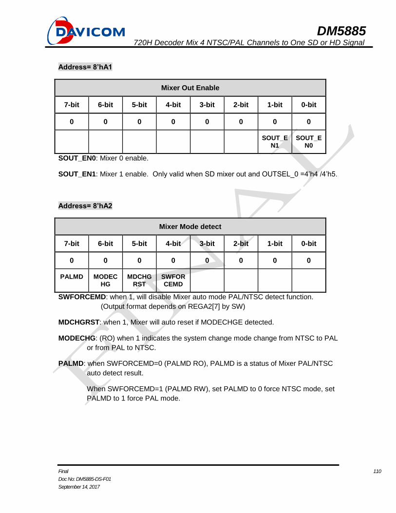
DM5885 720H Decoder Mix 4 NTSC/PAL Channels to One SD or HD Signal
Final 110
Doc No: DM5885-DS-F01
September 14, 2017
Address= 8’hA1
Mixer Out Enable
7-bit 6-bit 5-bit 4-bit 3-bit 2-bit 1-bit 0-bit
0 0 0 0 0 0 0 0
SOUT_EN1
SOUT_EN0
SOUT_EN0: Mixer 0 enable.
SOUT_EN1: Mixer 1 enable. Only valid when SD mixer out and OUTSEL_0 =4’h4 /4’h5.
Address= 8’hA2
Mixer Mode detect
7-bit 6-bit 5-bit 4-bit 3-bit 2-bit 1-bit 0-bit
0 0 0 0 0 0 0 0
PALMD MODECHG
MDCHGRST
SWFORCEMD
SWFORCEMD: when 1, will disable Mixer auto mode PAL/NTSC detect function.
(Output format depends on REGA2[7] by SW)
MDCHGRST: when 1, Mixer will auto reset if MODECHGE detected.
MODECHG: (RO) when 1 indicates the system change mode change from NTSC to PAL
or from PAL to NTSC.
PALMD: when SWFORCEMD=0 (PALMD RO), PALMD is a status of Mixer PAL/NTSC
auto detect result.
When SWFORCEMD=1 (PALMD RW), set PALMD to 0 force NTSC mode, set
PALMD to 1 force PAL mode.
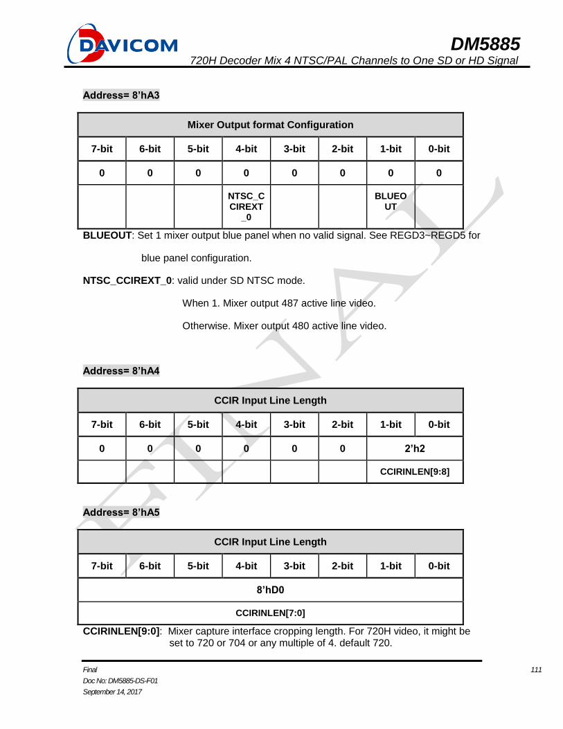
DM5885 720H Decoder Mix 4 NTSC/PAL Channels to One SD or HD Signal
Final 111
Doc No: DM5885-DS-F01
September 14, 2017
Address= 8’hA3
Mixer Output format Configuration
7-bit 6-bit 5-bit 4-bit 3-bit 2-bit 1-bit 0-bit
0 0 0 0 0 0 0 0
NTSC_CCIREXT
_0
BLUEOUT
BLUEOUT: Set 1 mixer output blue panel when no valid signal. See REGD3~REGD5 for
blue panel configuration.
NTSC_CCIREXT_0: valid under SD NTSC mode.
When 1. Mixer output 487 active line video.
Otherwise. Mixer output 480 active line video.
Address= 8’hA4
CCIR Input Line Length
7-bit 6-bit 5-bit 4-bit 3-bit 2-bit 1-bit 0-bit
0 0 0 0 0 0 2’h2
CCIRINLEN[9:8]
Address= 8’hA5
CCIR Input Line Length
7-bit 6-bit 5-bit 4-bit 3-bit 2-bit 1-bit 0-bit
8’hD0
CCIRINLEN[7:0]
CCIRINLEN[9:0]: Mixer capture interface cropping length. For 720H video, it might be set to 720 or 704 or any multiple of 4. default 720.
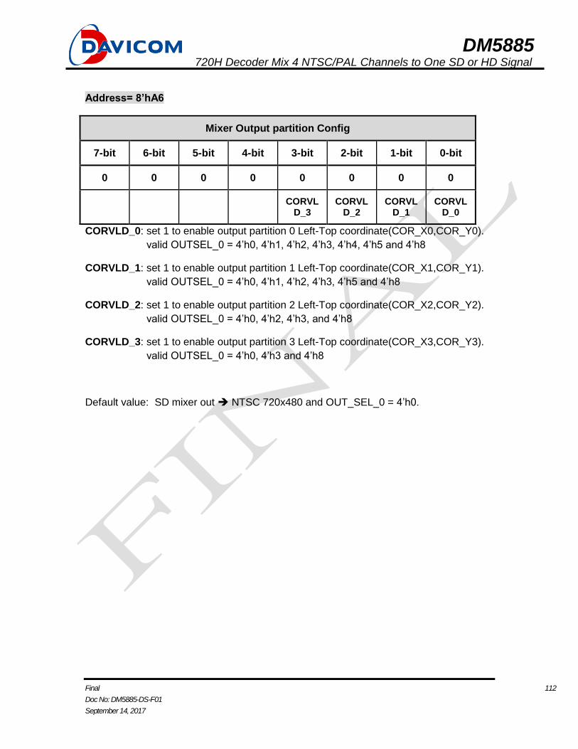
DM5885 720H Decoder Mix 4 NTSC/PAL Channels to One SD or HD Signal
Final 112
Doc No: DM5885-DS-F01
September 14, 2017
Address= 8’hA6
Mixer Output partition Config
7-bit 6-bit 5-bit 4-bit 3-bit 2-bit 1-bit 0-bit
0 0 0 0 0 0 0 0
CORVLD_3
CORVLD_2
CORVLD_1
CORVLD_0
CORVLD_0: set 1 to enable output partition 0 Left-Top coordinate(COR_X0,COR_Y0).
valid OUTSEL_0 = 4’h0, 4’h1, 4’h2, 4’h3, 4’h4, 4’h5 and 4’h8
CORVLD_1: set 1 to enable output partition 1 Left-Top coordinate(COR_X1,COR_Y1).
valid OUTSEL_0 = 4’h0, 4’h1, 4’h2, 4’h3, 4’h5 and 4’h8
CORVLD_2: set 1 to enable output partition 2 Left-Top coordinate(COR_X2,COR_Y2).
valid OUTSEL_0 = 4’h0, 4’h2, 4’h3, and 4’h8
CORVLD_3: set 1 to enable output partition 3 Left-Top coordinate(COR_X3,COR_Y3).
valid OUTSEL_0 = 4’h0, 4’h3 and 4’h8
Default value: SD mixer out NTSC 720x480 and OUT_SEL_0 = 4’h0.
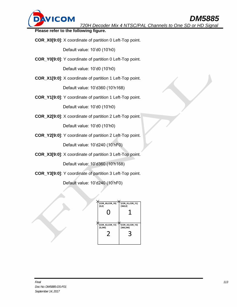
DM5885 720H Decoder Mix 4 NTSC/PAL Channels to One SD or HD Signal
Final 113
Doc No: DM5885-DS-F01
September 14, 2017
Please refer to the following figure.
COR_X0[9:0]: X coordinate of partition 0 Left-Top point.
Default value: 10’d0 (10’h0)
COR_Y0[9:0]: Y coordinate of partition 0 Left-Top point.
Default value: 10’d0 (10’h0)
COR_X1[9:0]: X coordinate of partition 1 Left-Top point.
Default value: 10’d360 (10’h168)
COR_Y1[9:0]: Y coordinate of partition 1 Left-Top point.
Default value: 10’d0 (10’h0)
COR_X2[9:0]: X coordinate of partition 2 Left-Top point.
Default value: 10’d0 (10’h0)
COR_Y2[9:0]: Y coordinate of partition 2 Left-Top point.
Default value: 10’d240 (10’hF0)
COR_X3[9:0]: X coordinate of partition 3 Left-Top point.
Default value: 10’d360 (10’h168)
COR_Y3[9:0]: Y coordinate of partition 3 Left-Top point.
Default value: 10’d240 (10’hF0)
0 1
2 3
[COR_X0,COR_Y0][0,0]
[COR_X1,COR_Y1][360,0]
[COR_X2,COR_Y2][0,240]
[COR_X3,COR_Y3][360,240]
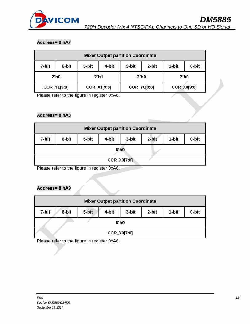
DM5885 720H Decoder Mix 4 NTSC/PAL Channels to One SD or HD Signal
Final 114
Doc No: DM5885-DS-F01
September 14, 2017
Address= 8’hA7
Mixer Output partition Coordinate
7-bit 6-bit 5-bit 4-bit 3-bit 2-bit 1-bit 0-bit
2’h0 2’h1 2’h0 2’h0
COR_Y1[9:8] COR_X1[9:8] COR_Y0[9:8] COR_X0[9:8]
Please refer to the figure in register 0xA6.
Address= 8’hA8
Mixer Output partition Coordinate
7-bit 6-bit 5-bit 4-bit 3-bit 2-bit 1-bit 0-bit
8’h0
COR_X0[7:0]
Please refer to the figure in register 0xA6.
Address= 8’hA9
Mixer Output partition Coordinate
7-bit 6-bit 5-bit 4-bit 3-bit 2-bit 1-bit 0-bit
8’h0
COR_Y0[7:0]
Please refer to the figure in register 0xA6.
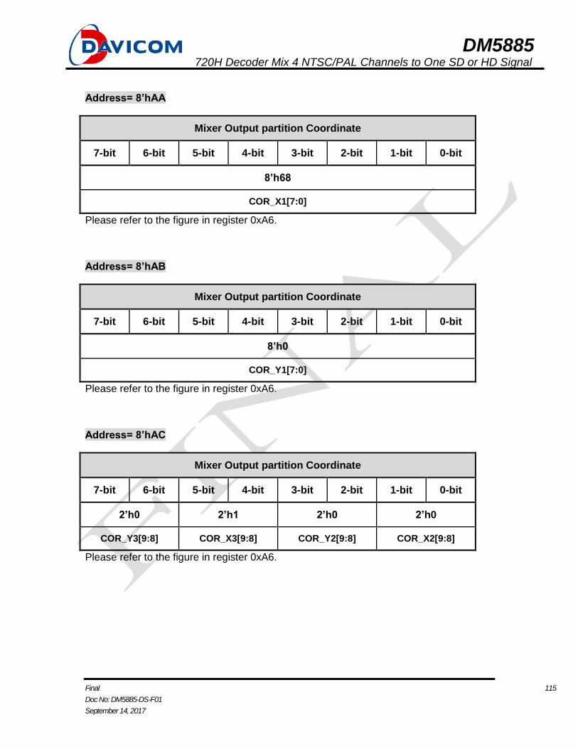
DM5885 720H Decoder Mix 4 NTSC/PAL Channels to One SD or HD Signal
Final 115
Doc No: DM5885-DS-F01
September 14, 2017
Address= 8’hAA
Mixer Output partition Coordinate
7-bit 6-bit 5-bit 4-bit 3-bit 2-bit 1-bit 0-bit
8’h68
COR_X1[7:0]
Please refer to the figure in register 0xA6.
Address= 8’hAB
Mixer Output partition Coordinate
7-bit 6-bit 5-bit 4-bit 3-bit 2-bit 1-bit 0-bit
8’h0
COR_Y1[7:0]
Please refer to the figure in register 0xA6.
Address= 8’hAC
Mixer Output partition Coordinate
7-bit 6-bit 5-bit 4-bit 3-bit 2-bit 1-bit 0-bit
2’h0 2’h1 2’h0 2’h0
COR_Y3[9:8] COR_X3[9:8] COR_Y2[9:8] COR_X2[9:8]
Please refer to the figure in register 0xA6.
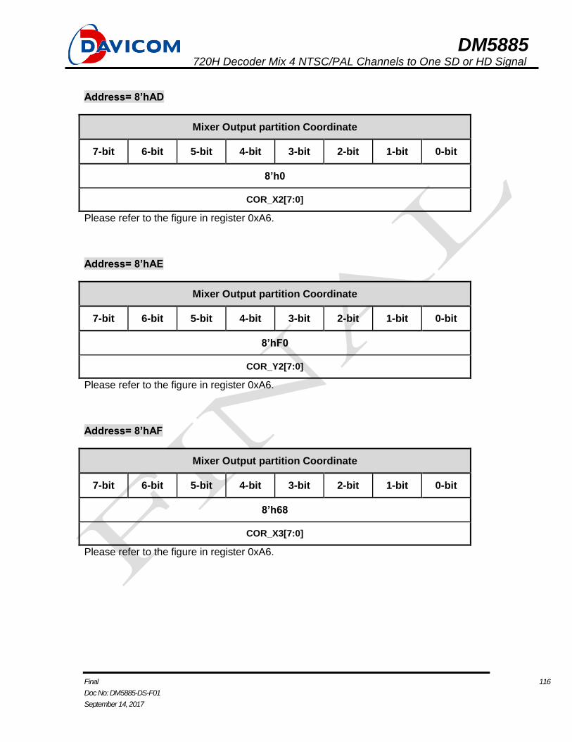
DM5885 720H Decoder Mix 4 NTSC/PAL Channels to One SD or HD Signal
Final 116
Doc No: DM5885-DS-F01
September 14, 2017
Address= 8’hAD
Mixer Output partition Coordinate
7-bit 6-bit 5-bit 4-bit 3-bit 2-bit 1-bit 0-bit
8’h0
COR_X2[7:0]
Please refer to the figure in register 0xA6.
Address= 8’hAE
Mixer Output partition Coordinate
7-bit 6-bit 5-bit 4-bit 3-bit 2-bit 1-bit 0-bit
8’hF0
COR_Y2[7:0]
Please refer to the figure in register 0xA6.
Address= 8’hAF
Mixer Output partition Coordinate
7-bit 6-bit 5-bit 4-bit 3-bit 2-bit 1-bit 0-bit
8’h68
COR_X3[7:0]
Please refer to the figure in register 0xA6.
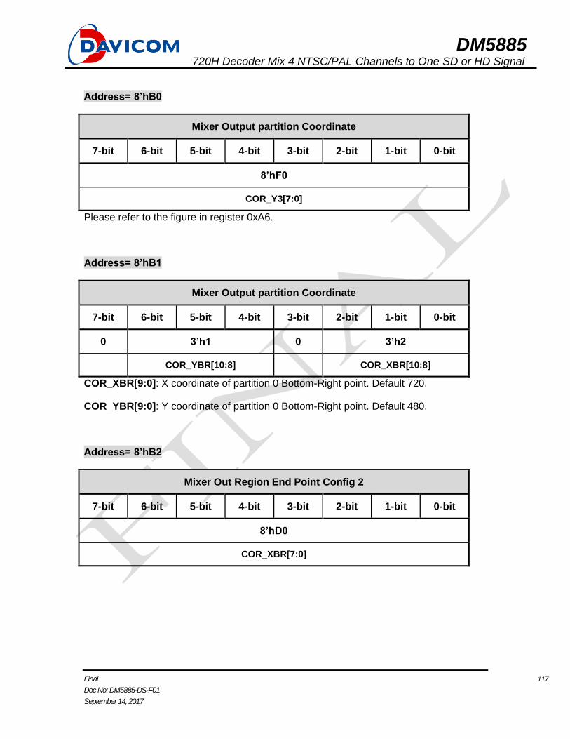
DM5885 720H Decoder Mix 4 NTSC/PAL Channels to One SD or HD Signal
Final 117
Doc No: DM5885-DS-F01
September 14, 2017
Address= 8’hB0
Mixer Output partition Coordinate
7-bit 6-bit 5-bit 4-bit 3-bit 2-bit 1-bit 0-bit
8’hF0
COR_Y3[7:0]
Please refer to the figure in register 0xA6.
Address= 8’hB1
Mixer Output partition Coordinate
7-bit 6-bit 5-bit 4-bit 3-bit 2-bit 1-bit 0-bit
0 3’h1 0 3’h2
COR_YBR[10:8] COR_XBR[10:8]
COR_XBR[9:0]: X coordinate of partition 0 Bottom-Right point. Default 720.
COR_YBR[9:0]: Y coordinate of partition 0 Bottom-Right point. Default 480.
Address= 8’hB2
Mixer Out Region End Point Config 2
7-bit 6-bit 5-bit 4-bit 3-bit 2-bit 1-bit 0-bit
8’hD0
COR_XBR[7:0]
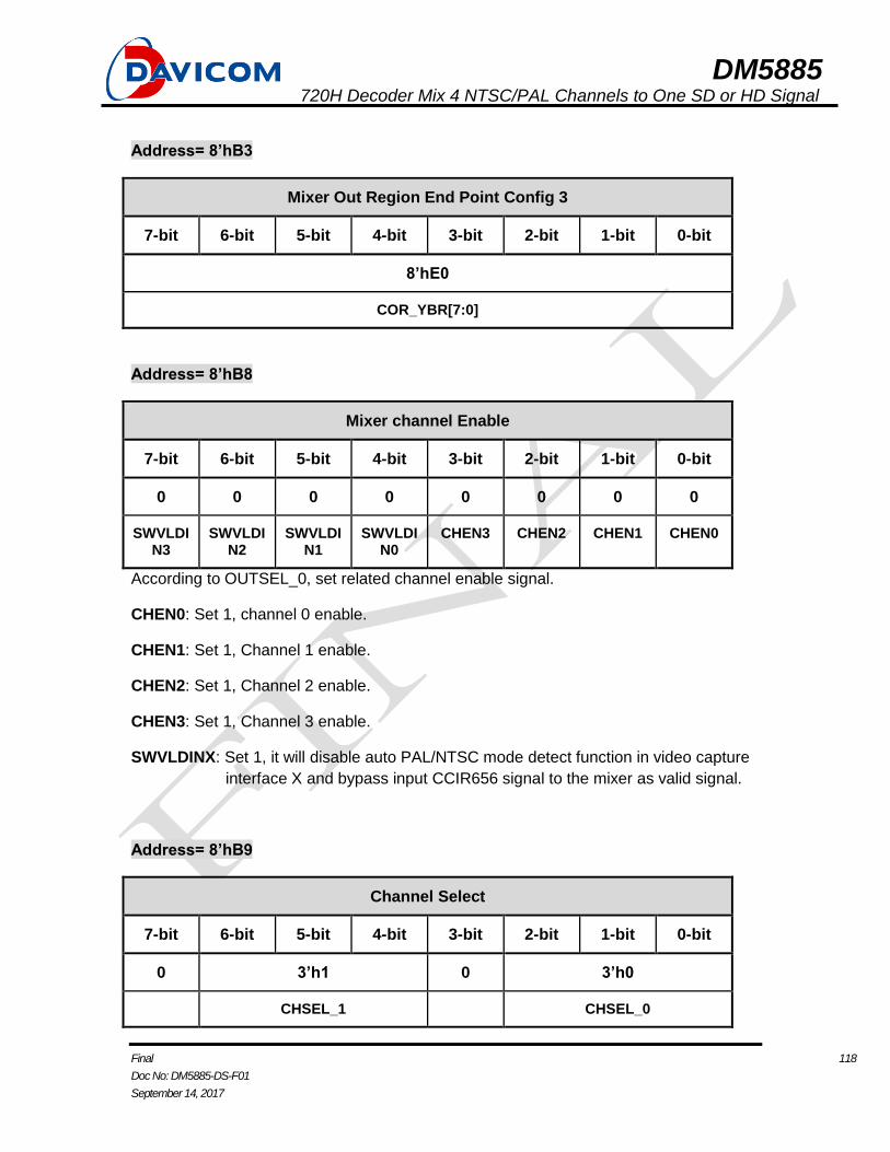
DM5885 720H Decoder Mix 4 NTSC/PAL Channels to One SD or HD Signal
Final 118
Doc No: DM5885-DS-F01
September 14, 2017
Address= 8’hB3
Mixer Out Region End Point Config 3
7-bit 6-bit 5-bit 4-bit 3-bit 2-bit 1-bit 0-bit
8’hE0
COR_YBR[7:0]
Address= 8’hB8
Mixer channel Enable
7-bit 6-bit 5-bit 4-bit 3-bit 2-bit 1-bit 0-bit
0 0 0 0 0 0 0 0
SWVLDIN3
SWVLDIN2
SWVLDIN1
SWVLDIN0
CHEN3 CHEN2 CHEN1 CHEN0
According to OUTSEL_0, set related channel enable signal.
CHEN0: Set 1, channel 0 enable.
CHEN1: Set 1, Channel 1 enable.
CHEN2: Set 1, Channel 2 enable.
CHEN3: Set 1, Channel 3 enable.
SWVLDINX: Set 1, it will disable auto PAL/NTSC mode detect function in video capture
interface X and bypass input CCIR656 signal to the mixer as valid signal.
Address= 8’hB9
Channel Select
7-bit 6-bit 5-bit 4-bit 3-bit 2-bit 1-bit 0-bit
0 3’h1 0 3’h0
CHSEL_1 CHSEL_0
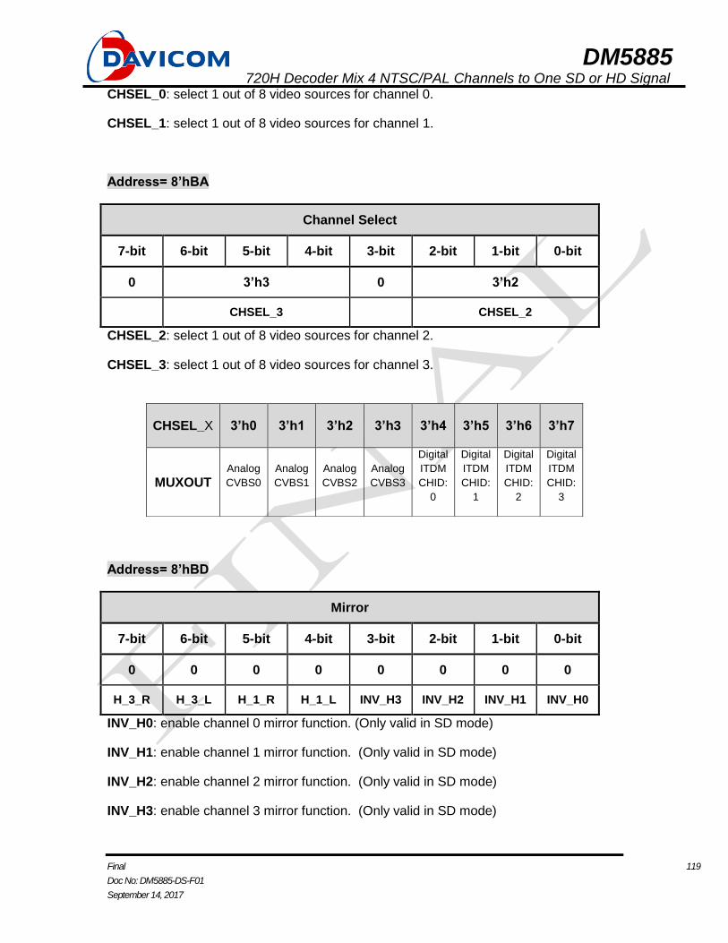
DM5885 720H Decoder Mix 4 NTSC/PAL Channels to One SD or HD Signal
Final 119
Doc No: DM5885-DS-F01
September 14, 2017
CHSEL_0: select 1 out of 8 video sources for channel 0.
CHSEL_1: select 1 out of 8 video sources for channel 1.
Address= 8’hBA
Channel Select
7-bit 6-bit 5-bit 4-bit 3-bit 2-bit 1-bit 0-bit
0 3’h3 0 3’h2
CHSEL_3 CHSEL_2
CHSEL_2: select 1 out of 8 video sources for channel 2.
CHSEL_3: select 1 out of 8 video sources for channel 3.
Address= 8’hBD
Mirror
7-bit 6-bit 5-bit 4-bit 3-bit 2-bit 1-bit 0-bit
0 0 0 0 0 0 0 0
H_3_R H_3_L H_1_R H_1_L INV_H3 INV_H2 INV_H1 INV_H0
INV_H0: enable channel 0 mirror function. (Only valid in SD mode)
INV_H1: enable channel 1 mirror function. (Only valid in SD mode)
INV_H2: enable channel 2 mirror function. (Only valid in SD mode)
INV_H3: enable channel 3 mirror function. (Only valid in SD mode)
CHSEL_X 3’h0 3’h1 3’h2 3’h3 3’h4 3’h5 3’h6 3’h7
MUXOUT Analog
CVBS0
Analog
CVBS1
Analog
CVBS2
Analog
CVBS3
Digital
ITDM
CHID:
0
Digital
ITDM
CHID:
1
Digital
ITDM
CHID:
2
Digital
ITDM
CHID:
3
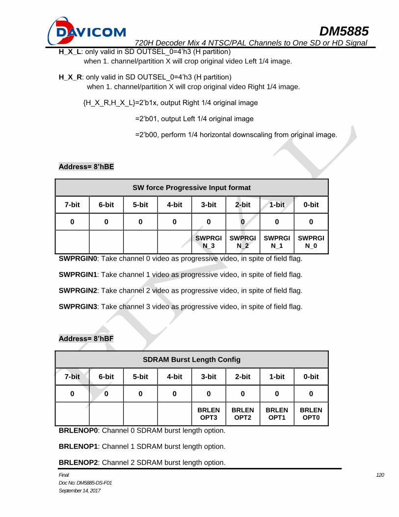
DM5885 720H Decoder Mix 4 NTSC/PAL Channels to One SD or HD Signal
Final 120
Doc No: DM5885-DS-F01
September 14, 2017
H_X_L: only valid in SD OUTSEL_0=4’h3 (H partition)
when 1. channel/partition X will crop original video Left 1/4 image.
H_X_R: only valid in SD OUTSEL_0=4’h3 (H partition)
when 1. channel/partition X will crop original video Right 1/4 image.
{H_X_R,H_X_L}=2’b1x, output Right 1/4 original image
=2’b01, output Left 1/4 original image
=2’b00, perform 1/4 horizontal downscaling from original image.
Address= 8’hBE
SW force Progressive Input format
7-bit 6-bit 5-bit 4-bit 3-bit 2-bit 1-bit 0-bit
0 0 0 0 0 0 0 0
SWPRGIN_3
SWPRGIN_2
SWPRGIN_1
SWPRGIN_0
SWPRGIN0: Take channel 0 video as progressive video, in spite of field flag.
SWPRGIN1: Take channel 1 video as progressive video, in spite of field flag.
SWPRGIN2: Take channel 2 video as progressive video, in spite of field flag.
SWPRGIN3: Take channel 3 video as progressive video, in spite of field flag.
Address= 8’hBF
SDRAM Burst Length Config
7-bit 6-bit 5-bit 4-bit 3-bit 2-bit 1-bit 0-bit
0 0 0 0 0 0 0 0
BRLENOPT3
BRLENOPT2
BRLENOPT1
BRLENOPT0
BRLENOP0: Channel 0 SDRAM burst length option.
BRLENOP1: Channel 1 SDRAM burst length option.
BRLENOP2: Channel 2 SDRAM burst length option.
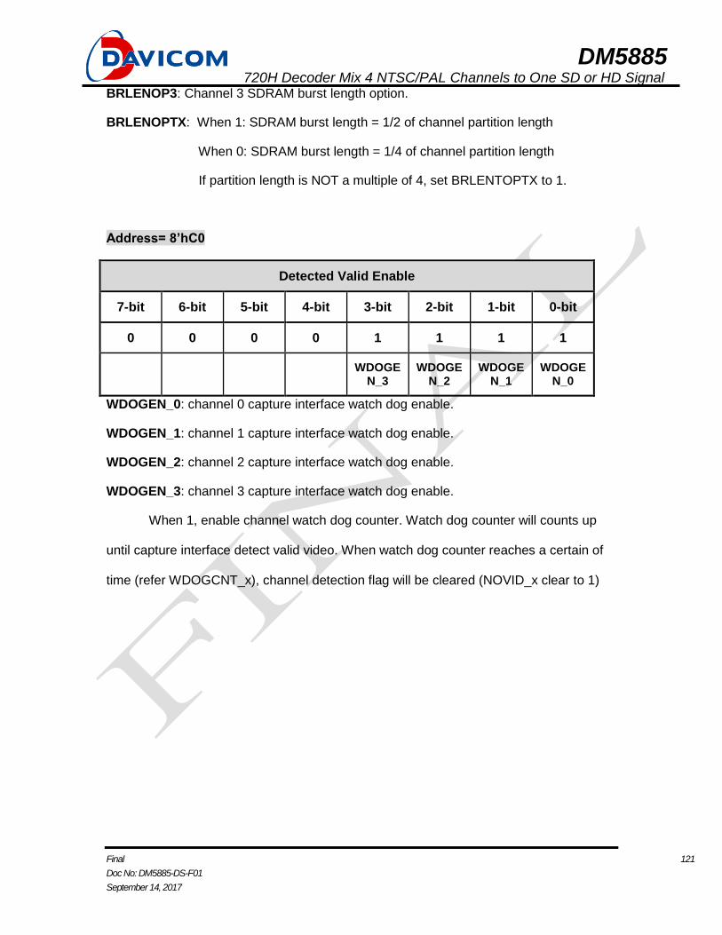
DM5885 720H Decoder Mix 4 NTSC/PAL Channels to One SD or HD Signal
Final 121
Doc No: DM5885-DS-F01
September 14, 2017
BRLENOP3: Channel 3 SDRAM burst length option.
BRLENOPTX: When 1: SDRAM burst length = 1/2 of channel partition length
When 0: SDRAM burst length = 1/4 of channel partition length
If partition length is NOT a multiple of 4, set BRLENTOPTX to 1.
Address= 8’hC0
Detected Valid Enable
7-bit 6-bit 5-bit 4-bit 3-bit 2-bit 1-bit 0-bit
0 0 0 0 1 1 1 1
WDOGEN_3
WDOGEN_2
WDOGEN_1
WDOGEN_0
WDOGEN_0: channel 0 capture interface watch dog enable.
WDOGEN_1: channel 1 capture interface watch dog enable.
WDOGEN_2: channel 2 capture interface watch dog enable.
WDOGEN_3: channel 3 capture interface watch dog enable.
When 1, enable channel watch dog counter. Watch dog counter will counts up
until capture interface detect valid video. When watch dog counter reaches a certain of
time (refer WDOGCNT_x), channel detection flag will be cleared (NOVID_x clear to 1)
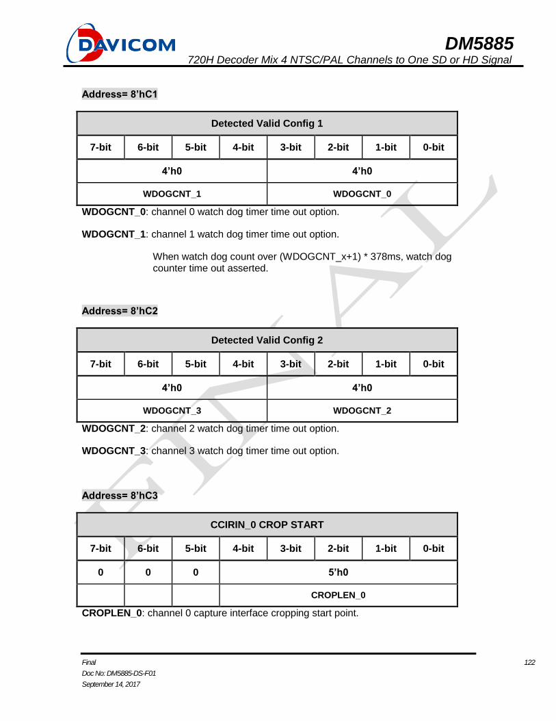
DM5885 720H Decoder Mix 4 NTSC/PAL Channels to One SD or HD Signal
Final 122
Doc No: DM5885-DS-F01
September 14, 2017
Address= 8’hC1
Detected Valid Config 1
7-bit 6-bit 5-bit 4-bit 3-bit 2-bit 1-bit 0-bit
4’h0 4’h0
WDOGCNT_1 WDOGCNT_0
WDOGCNT_0: channel 0 watch dog timer time out option.
WDOGCNT_1: channel 1 watch dog timer time out option.
When watch dog count over (WDOGCNT_x+1) * 378ms, watch dog counter time out asserted.
Address= 8’hC2
Detected Valid Config 2
7-bit 6-bit 5-bit 4-bit 3-bit 2-bit 1-bit 0-bit
4’h0 4’h0
WDOGCNT_3 WDOGCNT_2
WDOGCNT_2: channel 2 watch dog timer time out option.
WDOGCNT_3: channel 3 watch dog timer time out option.
Address= 8’hC3
CCIRIN_0 CROP START
7-bit 6-bit 5-bit 4-bit 3-bit 2-bit 1-bit 0-bit
0 0 0 5’h0
CROPLEN_0
CROPLEN_0: channel 0 capture interface cropping start point.

DM5885 720H Decoder Mix 4 NTSC/PAL Channels to One SD or HD Signal
Final 123
Doc No: DM5885-DS-F01
September 14, 2017
Address= 8’hC4
CCIRIN_1 CROP START
7-bit 6-bit 5-bit 4-bit 3-bit 2-bit 1-bit 0-bit
0 0 0 5’h0
CROPLEN_1
CROPLEN_1: channel 1 capture interface cropping start point.
Address= 8’hC5
CCIRIN_2 CROP START
7-bit 6-bit 5-bit 4-bit 3-bit 2-bit 1-bit 0-bit
0 0 0 5’h0
CROPLEN_2
CROPLEN_2: channel 2 capture interface cropping start point.
Address= 8’hC6
CCIRIN_3 CROP START
7-bit 6-bit 5-bit 4-bit 3-bit 2-bit 1-bit 0-bit
0 0 0 5’h0
CROPLEN_3
CROPLEN_3: channel 3 capture interface cropping start point.
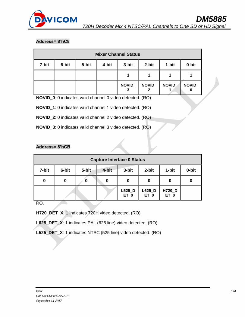
DM5885 720H Decoder Mix 4 NTSC/PAL Channels to One SD or HD Signal
Final 124
Doc No: DM5885-DS-F01
September 14, 2017
Address= 8’hC8
Mixer Channel Status
7-bit 6-bit 5-bit 4-bit 3-bit 2-bit 1-bit 0-bit
1 1 1 1
NOVID_3
NOVID_2
NOVID_1
NOVID_0
NOVID_0: 0 indicates valid channel 0 video detected. (RO)
NOVID_1: 0 indicates valid channel 1 video detected. (RO)
NOVID_2: 0 indicates valid channel 2 video detected. (RO)
NOVID_3: 0 indicates valid channel 3 video detected. (RO)
Address= 8’hCB
Capture Interface 0 Status
7-bit 6-bit 5-bit 4-bit 3-bit 2-bit 1-bit 0-bit
0 0 0 0 0 0 0 0
L525_DET_0
L625_DET_0
H720_DET_0
RO.
H720_DET_X: 1 indicates 720H video detected. (RO)
L625_DET_X: 1 indicates PAL (625 line) video detected. (RO)
L525_DET_X: 1 indicates NTSC (525 line) video detected. (RO)
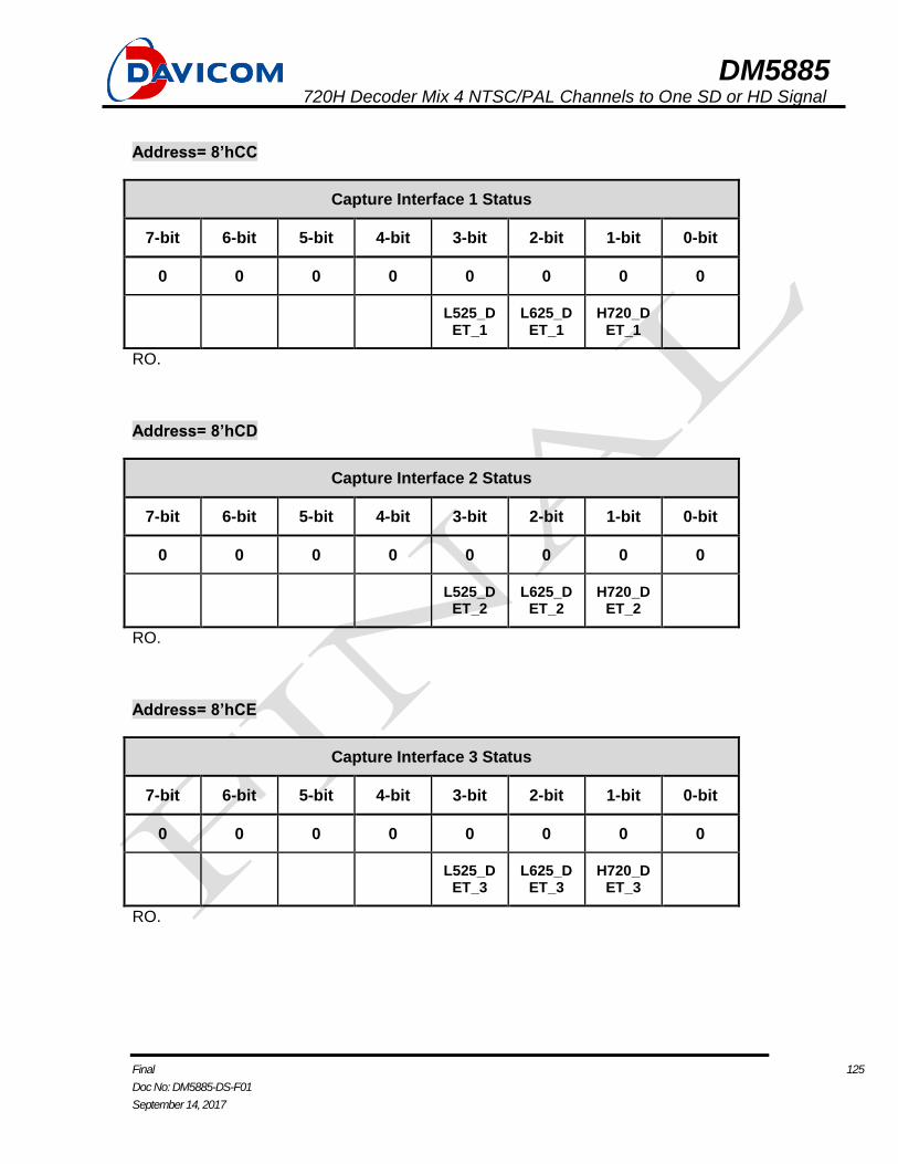
DM5885 720H Decoder Mix 4 NTSC/PAL Channels to One SD or HD Signal
Final 125
Doc No: DM5885-DS-F01
September 14, 2017
Address= 8’hCC
Capture Interface 1 Status
7-bit 6-bit 5-bit 4-bit 3-bit 2-bit 1-bit 0-bit
0 0 0 0 0 0 0 0
L525_DET_1
L625_DET_1
H720_DET_1
RO.
Address= 8’hCD
Capture Interface 2 Status
7-bit 6-bit 5-bit 4-bit 3-bit 2-bit 1-bit 0-bit
0 0 0 0 0 0 0 0
L525_DET_2
L625_DET_2
H720_DET_2
RO.
Address= 8’hCE
Capture Interface 3 Status
7-bit 6-bit 5-bit 4-bit 3-bit 2-bit 1-bit 0-bit
0 0 0 0 0 0 0 0
L525_DET_3
L625_DET_3
H720_DET_3
RO.
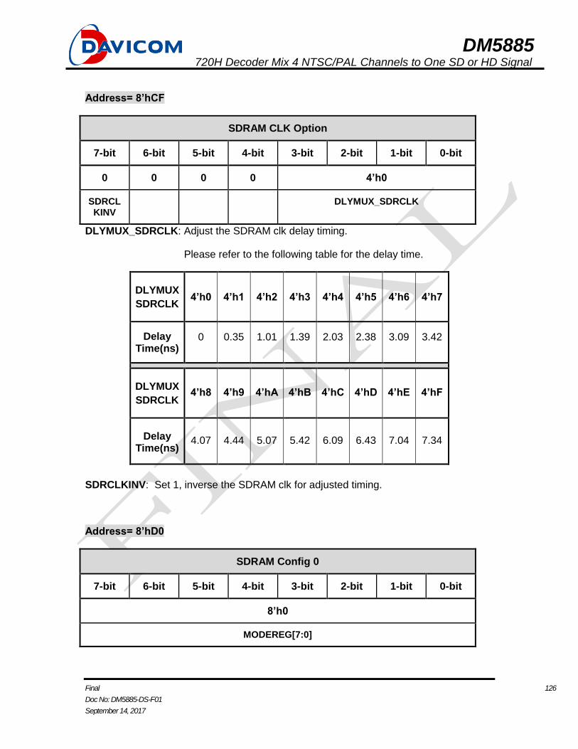
DM5885 720H Decoder Mix 4 NTSC/PAL Channels to One SD or HD Signal
Final 126
Doc No: DM5885-DS-F01
September 14, 2017
Address= 8’hCF
SDRAM CLK Option
7-bit 6-bit 5-bit 4-bit 3-bit 2-bit 1-bit 0-bit
0 0 0 0 4’h0
SDRCLKINV
DLYMUX_SDRCLK
DLYMUX_SDRCLK: Adjust the SDRAM clk delay timing.
Please refer to the following table for the delay time.
DLYMUX
SDRCLK 4’h0 4’h1 4’h2 4’h3 4’h4 4’h5 4’h6 4’h7
Delay Time(ns)
0 0.35 1.01 1.39 2.03 2.38 3.09 3.42
DLYMUX
SDRCLK 4’h8 4’h9 4’hA 4’hB 4’hC 4’hD 4’hE 4’hF
Delay Time(ns)
4.07 4.44 5.07 5.42 6.09 6.43 7.04 7.34
SDRCLKINV: Set 1, inverse the SDRAM clk for adjusted timing.
Address= 8’hD0
SDRAM Config 0
7-bit 6-bit 5-bit 4-bit 3-bit 2-bit 1-bit 0-bit
8’h0
MODEREG[7:0]
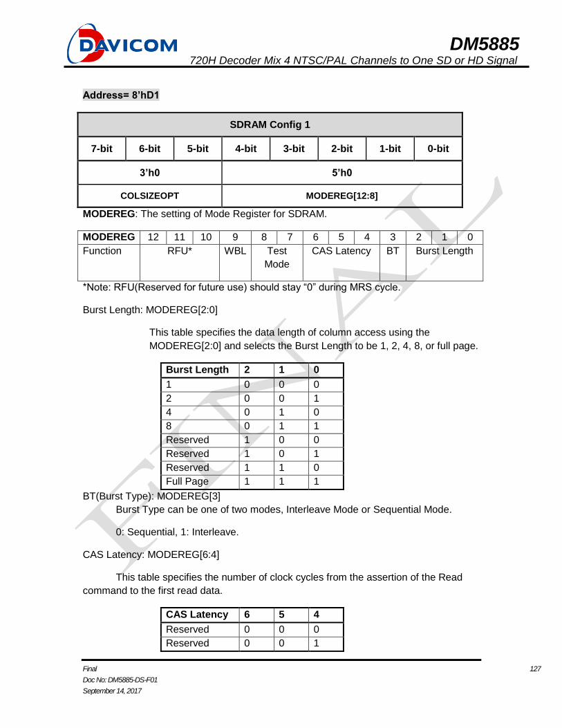
DM5885 720H Decoder Mix 4 NTSC/PAL Channels to One SD or HD Signal
Final 127
Doc No: DM5885-DS-F01
September 14, 2017
Address= 8’hD1
SDRAM Config 1
7-bit 6-bit 5-bit 4-bit 3-bit 2-bit 1-bit 0-bit
3’h0 5’h0
COLSIZEOPT MODEREG[12:8]
MODEREG: The setting of Mode Register for SDRAM.
MODEREG 12 11 10 9 8 7 6 5 4 3 2 1 0
Function RFU* WBL Test
Mode
CAS Latency BT Burst Length
*Note: RFU(Reserved for future use) should stay “0” during MRS cycle.
Burst Length: MODEREG[2:0]
This table specifies the data length of column access using the
MODEREG[2:0] and selects the Burst Length to be 1, 2, 4, 8, or full page.
Burst Length 2 1 0
1 0 0 0
2 0 0 1
4 0 1 0
8 0 1 1
Reserved 1 0 0
Reserved 1 0 1
Reserved 1 1 0
Full Page 1 1 1
BT(Burst Type): MODEREG[3]
Burst Type can be one of two modes, Interleave Mode or Sequential Mode.
0: Sequential, 1: Interleave.
CAS Latency: MODEREG[6:4]
This table specifies the number of clock cycles from the assertion of the Read
command to the first read data.
CAS Latency 6 5 4
Reserved 0 0 0
Reserved 0 0 1
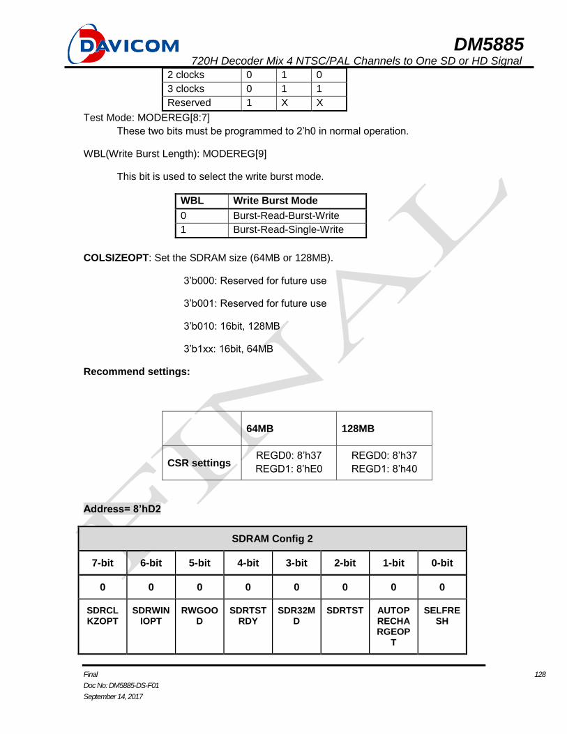
DM5885 720H Decoder Mix 4 NTSC/PAL Channels to One SD or HD Signal
Final 128
Doc No: DM5885-DS-F01
September 14, 2017
2 clocks 0 1 0
3 clocks 0 1 1
Reserved 1 X X
Test Mode: MODEREG[8:7]
These two bits must be programmed to 2’h0 in normal operation.
WBL(Write Burst Length): MODEREG[9]
This bit is used to select the write burst mode.
WBL Write Burst Mode
0 Burst-Read-Burst-Write
1 Burst-Read-Single-Write
COLSIZEOPT: Set the SDRAM size (64MB or 128MB).
3’b000: Reserved for future use
3’b001: Reserved for future use
3’b010: 16bit, 128MB
3’b1xx: 16bit, 64MB
Recommend settings:
64MB 128MB
CSR settings REGD0: 8’h37
REGD1: 8’hE0
REGD0: 8’h37
REGD1: 8’h40
Address= 8’hD2
SDRAM Config 2
7-bit 6-bit 5-bit 4-bit 3-bit 2-bit 1-bit 0-bit
0 0 0 0 0 0 0 0
SDRCLKZOPT
SDRWINIOPT
RWGOOD
SDRTSTRDY
SDR32MD
SDRTST AUTOPRECHARGEOP
T
SELFRESH
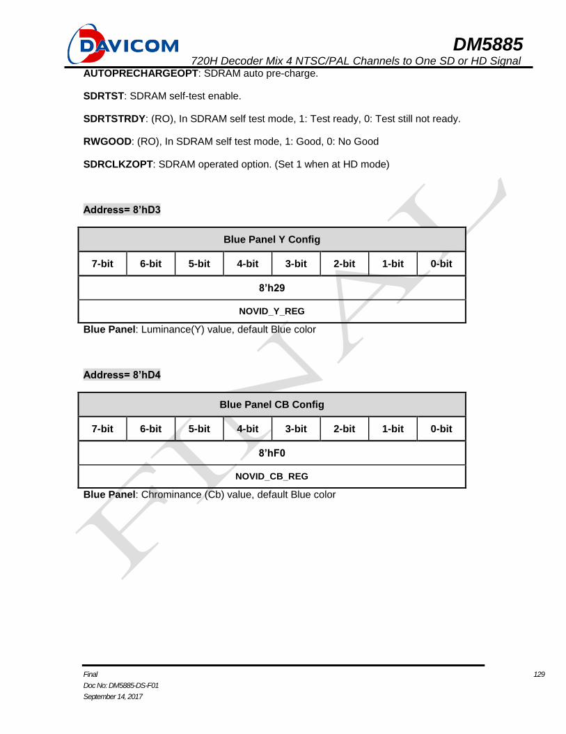
DM5885 720H Decoder Mix 4 NTSC/PAL Channels to One SD or HD Signal
Final 129
Doc No: DM5885-DS-F01
September 14, 2017
AUTOPRECHARGEOPT: SDRAM auto pre-charge.
SDRTST: SDRAM self-test enable.
SDRTSTRDY: (RO), In SDRAM self test mode, 1: Test ready, 0: Test still not ready.
RWGOOD: (RO), In SDRAM self test mode, 1: Good, 0: No Good
SDRCLKZOPT: SDRAM operated option. (Set 1 when at HD mode)
Address= 8’hD3
Blue Panel Y Config
7-bit 6-bit 5-bit 4-bit 3-bit 2-bit 1-bit 0-bit
8’h29
NOVID_Y_REG
Blue Panel: Luminance(Y) value, default Blue color
Address= 8’hD4
Blue Panel CB Config
7-bit 6-bit 5-bit 4-bit 3-bit 2-bit 1-bit 0-bit
8’hF0
NOVID_CB_REG
Blue Panel: Chrominance (Cb) value, default Blue color
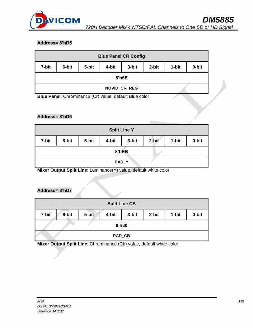
DM5885 720H Decoder Mix 4 NTSC/PAL Channels to One SD or HD Signal
Final 130
Doc No: DM5885-DS-F01
September 14, 2017
Address= 8’hD5
Blue Panel CR Config
7-bit 6-bit 5-bit 4-bit 3-bit 2-bit 1-bit 0-bit
8’h6E
NOVID_CR_REG
Blue Panel: Chrominance (Cr) value, default Blue color
Address= 8’hD6
Split Line Y
7-bit 6-bit 5-bit 4-bit 3-bit 2-bit 1-bit 0-bit
8’hEB
PAD_Y
Mixer Output Split Line: Luminance(Y) value, default white color
Address= 8’hD7
Split Line CB
7-bit 6-bit 5-bit 4-bit 3-bit 2-bit 1-bit 0-bit
8’h80
PAD_CB
Mixer Output Split Line: Chrominance (Cb) value, default white color
DM5885 720H Decoder Mix 4 NTSC/PAL Channels to One SD or HD Signal
Final 131
Doc No: DM5885-DS-F01
September 14, 2017
Address= 8’hD8
Split Line CR
7-bit 6-bit 5-bit 4-bit 3-bit 2-bit 1-bit 0-bit
8’h80
PAD_CR
Mixer Output Split Line: Chrominance (Cr) value, default white color
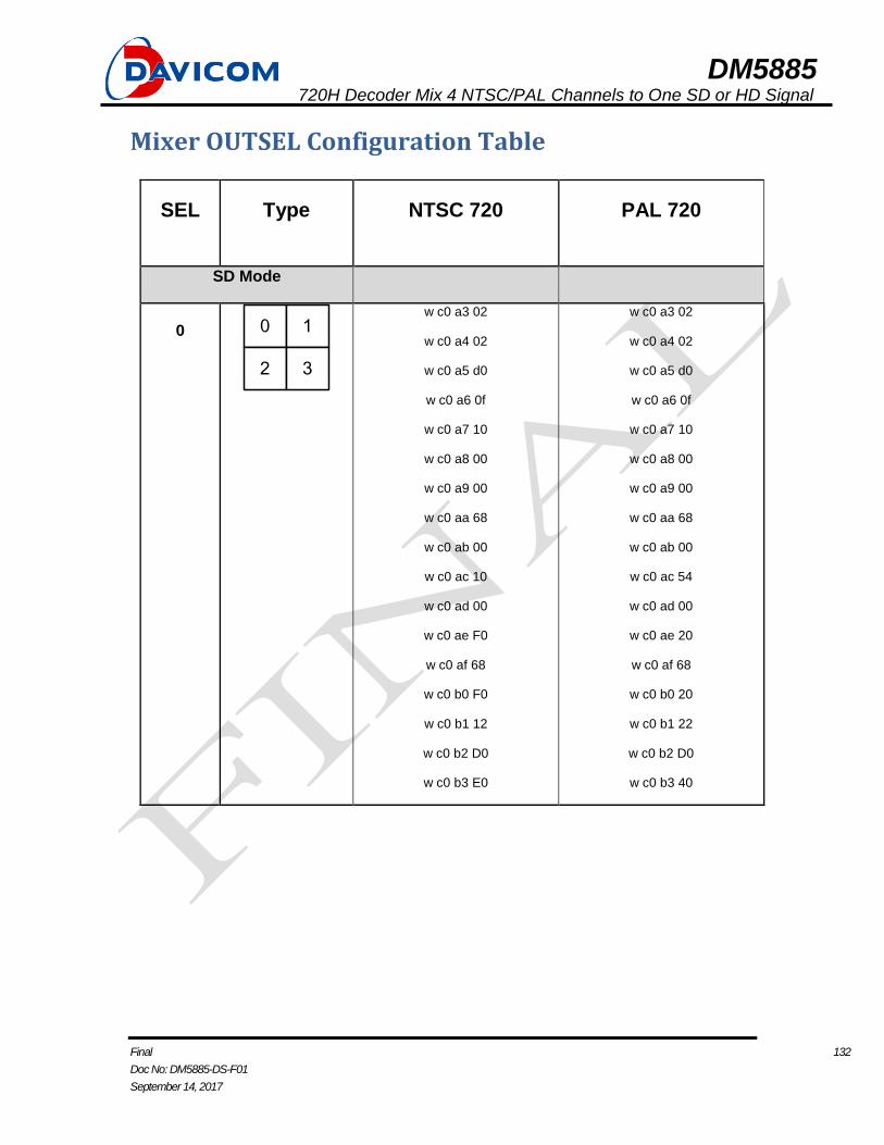
DM5885 720H Decoder Mix 4 NTSC/PAL Channels to One SD or HD Signal
Final 132
Doc No: DM5885-DS-F01
September 14, 2017
Mixer OUTSEL Configuration Table
SEL Type NTSC 720 PAL 720
SD Mode
0 0 1
2 3
w c0 a3 02
w c0 a4 02
w c0 a5 d0
w c0 a6 0f
w c0 a7 10
w c0 a8 00
w c0 a9 00
w c0 aa 68
w c0 ab 00
w c0 ac 10
w c0 ad 00
w c0 ae F0
w c0 af 68
w c0 b0 F0
w c0 b1 12
w c0 b2 D0
w c0 b3 E0
w c0 a3 02
w c0 a4 02
w c0 a5 d0
w c0 a6 0f
w c0 a7 10
w c0 a8 00
w c0 a9 00
w c0 aa 68
w c0 ab 00
w c0 ac 54
w c0 ad 00
w c0 ae 20
w c0 af 68
w c0 b0 20
w c0 b1 22
w c0 b2 D0
w c0 b3 40
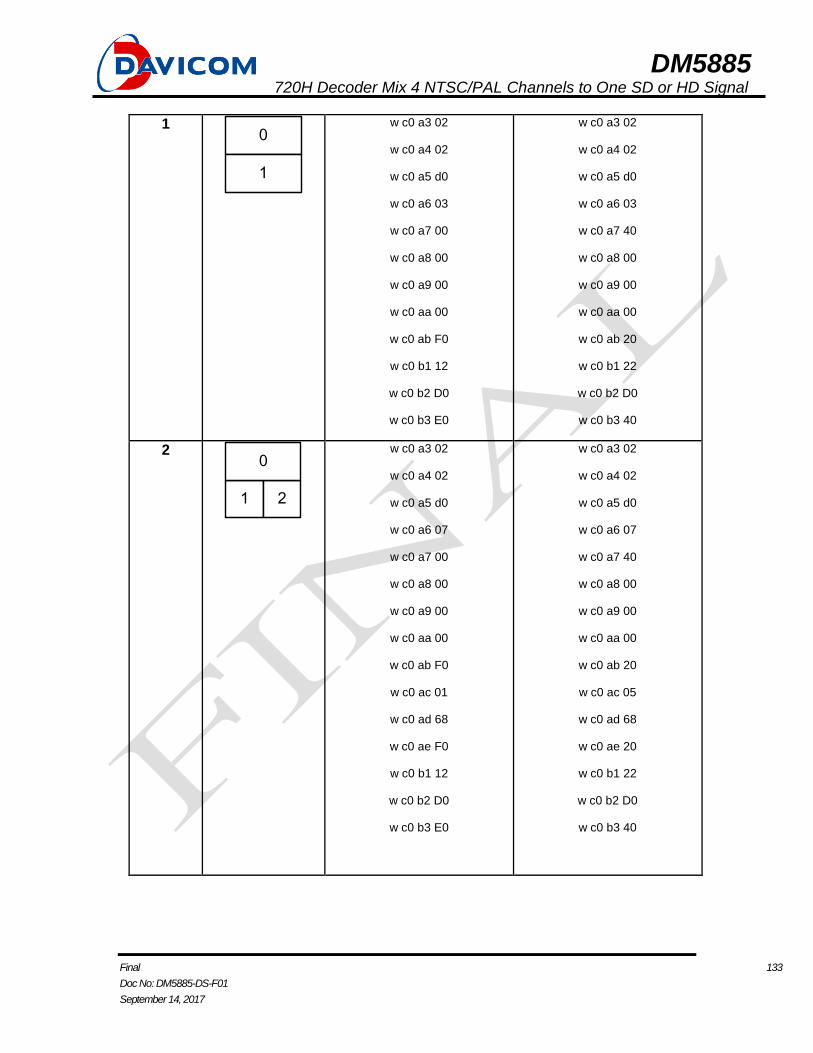
DM5885 720H Decoder Mix 4 NTSC/PAL Channels to One SD or HD Signal
Final 133
Doc No: DM5885-DS-F01
September 14, 2017
1 0
1
w c0 a3 02
w c0 a4 02
w c0 a5 d0
w c0 a6 03
w c0 a7 00
w c0 a8 00
w c0 a9 00
w c0 aa 00
w c0 ab F0
w c0 b1 12
w c0 b2 D0
w c0 b3 E0
w c0 a3 02
w c0 a4 02
w c0 a5 d0
w c0 a6 03
w c0 a7 40
w c0 a8 00
w c0 a9 00
w c0 aa 00
w c0 ab 20
w c0 b1 22
w c0 b2 D0
w c0 b3 40
2
1 2
0
w c0 a3 02
w c0 a4 02
w c0 a5 d0
w c0 a6 07
w c0 a7 00
w c0 a8 00
w c0 a9 00
w c0 aa 00
w c0 ab F0
w c0 ac 01
w c0 ad 68
w c0 ae F0
w c0 b1 12
w c0 b2 D0
w c0 b3 E0
w c0 a3 02
w c0 a4 02
w c0 a5 d0
w c0 a6 07
w c0 a7 40
w c0 a8 00
w c0 a9 00
w c0 aa 00
w c0 ab 20
w c0 ac 05
w c0 ad 68
w c0 ae 20
w c0 b1 22
w c0 b2 D0
w c0 b3 40

DM5885 720H Decoder Mix 4 NTSC/PAL Channels to One SD or HD Signal
Final 134
Doc No: DM5885-DS-F01
September 14, 2017
3
1
0
3
2
w c0 a3 02
w c0 a4 02
w c0 a5 d0
w c0 a6 0f
w c0 a7 00
w c0 a8 B4
w c0 a9 00
w c0 aa 00
w c0 ab 00
w c0 ac 20
w c0 ad B4
w c0 ae F0
w c0 af 1C
w c0 b0 00
w c0 b1 12
w c0 b2 D0
w c0 b3 E0
w c0 a3 02
w c0 a4 02
w c0 a5 d0
w c0 a6 0f
w c0 a7 00
w c0 a8 B4
w c0 a9 00
w c0 aa 00
w c0 ab 00
w c0 ac 24
w c0 ad B4
w c0 ae 20
w c0 af 1C
w c0 b0 00
w c0 b1 22
w c0 b2 D0
w c0 b3 40
4
0
w c0 a3 02
w c0 a4 02
w c0 a5 d0
w c0 a6 01
w c0 a7 00
w c0 a8 00
w c0 a9 00
w c0 b1 12
w c0 b2 D0
w c0 b3 E0
w c0 a3 02
w c0 a4 02
w c0 a5 d0
w c0 a6 01
w c0 a7 00
w c0 a8 00
w c0 a9 00
w c0 b1 22
w c0 b2 D0
w c0 b3 40
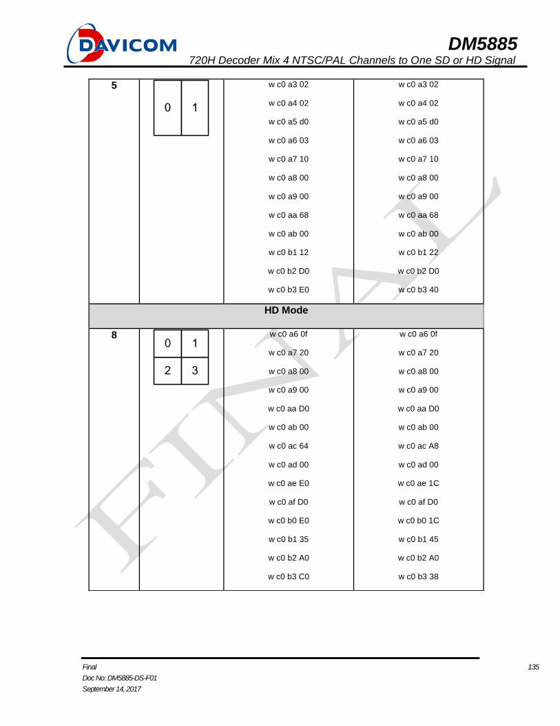
DM5885 720H Decoder Mix 4 NTSC/PAL Channels to One SD or HD Signal
Final 135
Doc No: DM5885-DS-F01
September 14, 2017
5
0 1
w c0 a3 02
w c0 a4 02
w c0 a5 d0
w c0 a6 03
w c0 a7 10
w c0 a8 00
w c0 a9 00
w c0 aa 68
w c0 ab 00
w c0 b1 12
w c0 b2 D0
w c0 b3 E0
w c0 a3 02
w c0 a4 02
w c0 a5 d0
w c0 a6 03
w c0 a7 10
w c0 a8 00
w c0 a9 00
w c0 aa 68
w c0 ab 00
w c0 b1 22
w c0 b2 D0
w c0 b3 40
HD Mode
8 0 1
2 3
w c0 a6 0f
w c0 a7 20
w c0 a8 00
w c0 a9 00
w c0 aa D0
w c0 ab 00
w c0 ac 64
w c0 ad 00
w c0 ae E0
w c0 af D0
w c0 b0 E0
w c0 b1 35
w c0 b2 A0
w c0 b3 C0
w c0 a6 0f
w c0 a7 20
w c0 a8 00
w c0 a9 00
w c0 aa D0
w c0 ab 00
w c0 ac A8
w c0 ad 00
w c0 ae 1C
w c0 af D0
w c0 b0 1C
w c0 b1 45
w c0 b2 A0
w c0 b3 38
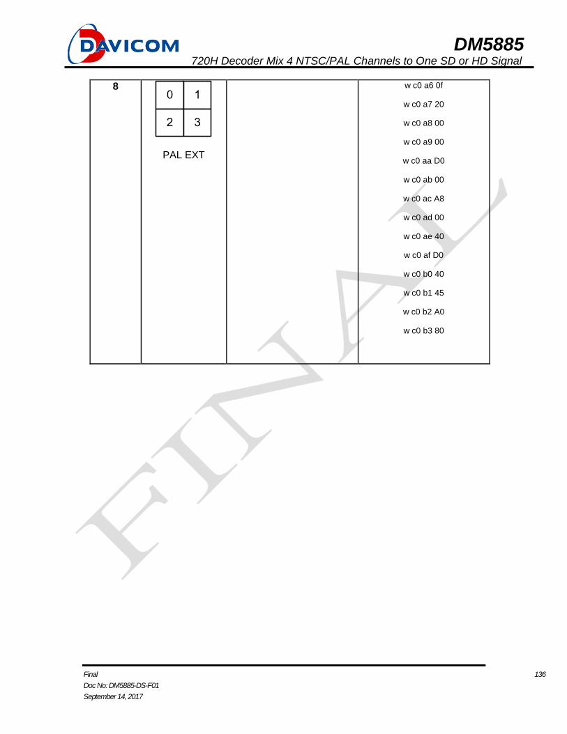
DM5885 720H Decoder Mix 4 NTSC/PAL Channels to One SD or HD Signal
Final 136
Doc No: DM5885-DS-F01
September 14, 2017
8 0 1
2 3
PAL EXT
w c0 a6 0f
w c0 a7 20
w c0 a8 00
w c0 a9 00
w c0 aa D0
w c0 ab 00
w c0 ac A8
w c0 ad 00
w c0 ae 40
w c0 af D0
w c0 b0 40
w c0 b1 45
w c0 b2 A0
w c0 b3 80
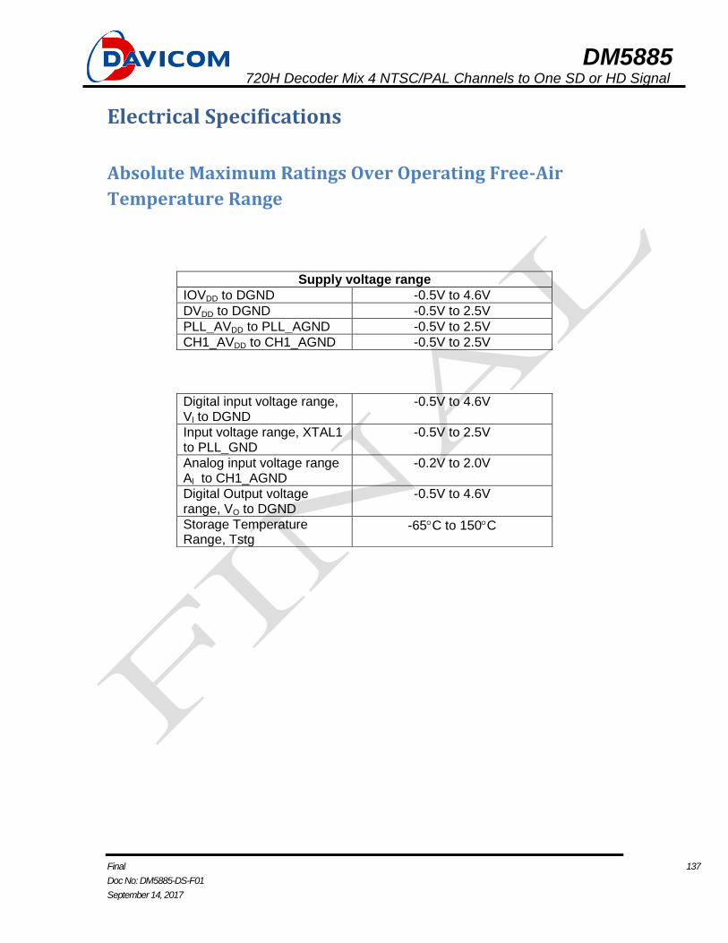
DM5885 720H Decoder Mix 4 NTSC/PAL Channels to One SD or HD Signal
Final 137
Doc No: DM5885-DS-F01
September 14, 2017
Electrical Specifications
Absolute Maximum Ratings Over Operating Free-Air
Temperature Range
Supply voltage range
IOVDD to DGND -0.5V to 4.6V
DVDD to DGND -0.5V to 2.5V
PLL_AVDD to PLL_AGND -0.5V to 2.5V
CH1_AVDD to CH1_AGND -0.5V to 2.5V
Digital input voltage range, Vl to DGND
-0.5V to 4.6V
Input voltage range, XTAL1 to PLL_GND
-0.5V to 2.5V
Analog input voltage range Al to CH1_AGND
-0.2V to 2.0V
Digital Output voltage range, VO to DGND
-0.5V to 4.6V
Storage Temperature Range, Tstg
-65C to 150C
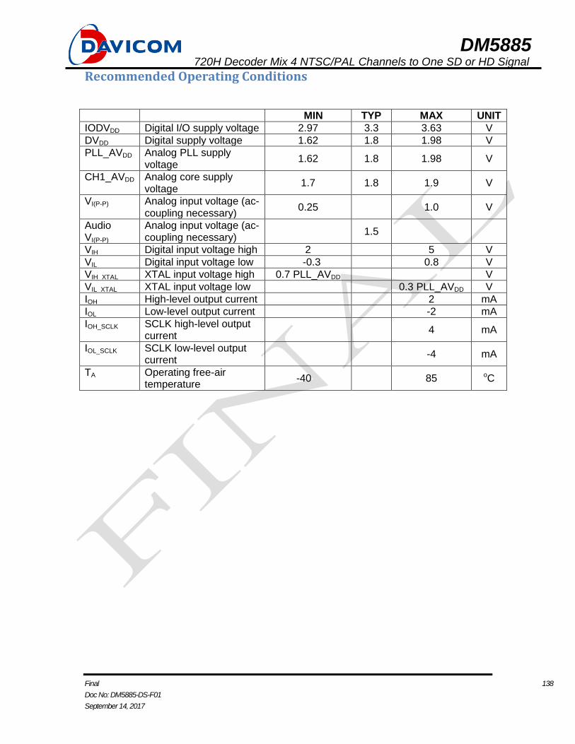
DM5885 720H Decoder Mix 4 NTSC/PAL Channels to One SD or HD Signal
Final 138
Doc No: DM5885-DS-F01
September 14, 2017
Recommended Operating Conditions
MIN TYP MAX UNIT
IODVDD Digital I/O supply voltage 2.97 3.3 3.63 V
DVDD Digital supply voltage 1.62 1.8 1.98 V
PLL_AVDD Analog PLL supply voltage
1.62 1.8 1.98 V
CH1_AVDD Analog core supply voltage
1.7 1.8 1.9 V
VI(P-P) Analog input voltage (ac-coupling necessary)
0.25 1.0 V
Audio VI(P-P)
Analog input voltage (ac-coupling necessary)
1.5
VIH Digital input voltage high 2 5 V
VIL Digital input voltage low -0.3 0.8 V
VIH_XTAL XTAL input voltage high 0.7 PLL_AVDD V
VIL_XTAL XTAL input voltage low 0.3 PLL_AVDD V
IOH High-level output current 2 mA
IOL Low-level output current -2 mA
IOH_SCLK SCLK high-level output current
4 mA
IOL_SCLK SCLK low-level output current
-4 mA
TA Operating free-air temperature
-40 85 oC

DM5885 720H Decoder Mix 4 NTSC/PAL Channels to One SD or HD Signal
Final 139
Doc No: DM5885-DS-F01
September 14, 2017
Crystal Specifications CRYSTAL
SPECIFICATIONS MIN NOM MAX UNIT
Frequency 27.0/36.0 MHz
Frequency tolerance 100 ppm
Electrical Characteristics DVDD = 1.8 V, PLL_AVDD = 1.8 V, CH1_AVDD = 1.8 V, IOVDD = 3.3 V
For minimum/maximum values: TA = -40C to 85C, and for typical values: TA = 25C
unless otherwise noted
DC Electrical Characteristics
PARAMETER TEST
CONDITIONS (see NOTE 1)
MIN TYP MAX UNIT
IDD(IO_D) Digital I/O supply current Color bar input 31.2 66.7 mA
IDD(D) Digital core supply current
Color bar input 212 297 mA
IDD(PLL_A) Analog PLL supply current
12
IDD(CH1-A) IDD(A) Analog ADC/DAC supply current
Color bar input 99.3 mA
PTOT Total power dissipation, normal mode
Color bar input 684.5 952.3 mW
PDOWN Total power dissipation, power-down mode
Color bar input 15.3 mW
Ci Input capacitance By design 8 pF
VOH Output voltage high IOH = 2 mA 0.8 IOVDD V
VOL Output voltage low IOL = -2 mA 0.22 IOVDD V
VOH_SCLK SCLK output voltage high
IOH = 4 mA 2.3 V
VOL_SCLK SCLK output voltage low IOL = -2 mA 0.6 V
NOTE 1: Measured with a load of 15 pf.
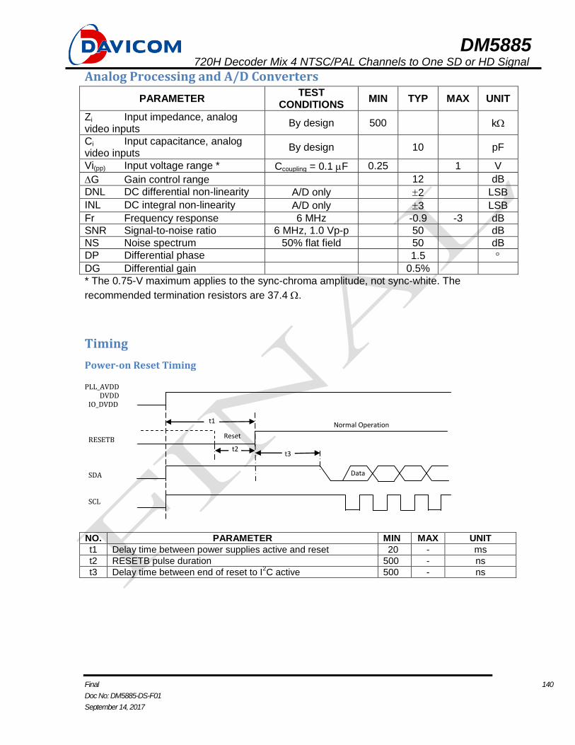
DM5885 720H Decoder Mix 4 NTSC/PAL Channels to One SD or HD Signal
Final 140
Doc No: DM5885-DS-F01
September 14, 2017
Analog Processing and A/D Converters
PARAMETER TEST
CONDITIONS MIN TYP MAX UNIT
Zi Input impedance, analog video inputs
By design 500 k
Ci Input capacitance, analog video inputs
By design 10 pF
Vi(pp) Input voltage range * Ccoupling = 0.1 F 0.25 1 V
G Gain control range 12 dB
DNL DC differential non-linearity A/D only 2 LSB
INL DC integral non-linearity A/D only 3 LSB
Fr Frequency response 6 MHz -0.9 -3 dB
SNR Signal-to-noise ratio 6 MHz, 1.0 Vp-p 50 dB
NS Noise spectrum 50% flat field 50 dB
DP Differential phase 1.5
DG Differential gain 0.5%
* The 0.75-V maximum applies to the sync-chroma amplitude, not sync-white. The
recommended termination resistors are 37.4 .
Timing
Power-on Reset Timing
PLL_AVDD DVDD
IO_DVDD RESETB SDA SCL
NO. PARAMETER MIN MAX UNIT
t1 Delay time between power supplies active and reset 20 - ms
t2 RESETB pulse duration 500 - ns
t3 Delay time between end of reset to I2C active 500 - ns
Reset
Normal Operation t1
t2 t3
Data
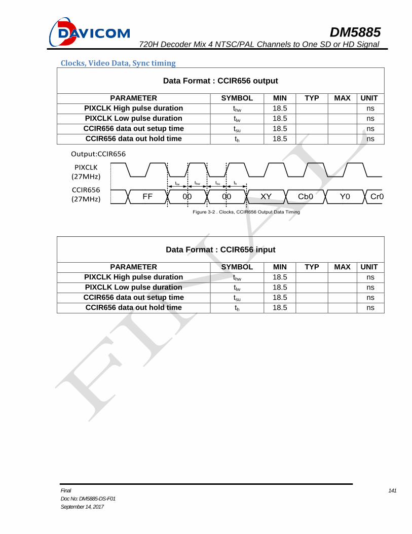
DM5885 720H Decoder Mix 4 NTSC/PAL Channels to One SD or HD Signal
Final 141
Doc No: DM5885-DS-F01
September 14, 2017
Clocks, Video Data, Sync timing
Data Format : CCIR656 output
PARAMETER SYMBOL MIN TYP MAX UNIT
PIXCLK High pulse duration thw 18.5 ns
PIXCLK Low pulse duration tlw 18.5 ns
CCIR656 data out setup time tsu 18.5 ns
CCIR656 data out hold time th 18.5 ns
Cr000 XY Cb0 Y000FF
PIXCLK(27MHz)
CCIR656(27MHz)
Output:CCIR656
tsu ththwtlw
Figure 3-2 . Clocks, CCIR656 Output Data Timing
Data Format : CCIR656 input
PARAMETER SYMBOL MIN TYP MAX UNIT
PIXCLK High pulse duration thw 18.5 ns
PIXCLK Low pulse duration tlw 18.5 ns
CCIR656 data out setup time tsu 18.5 ns
CCIR656 data out hold time th 18.5 ns
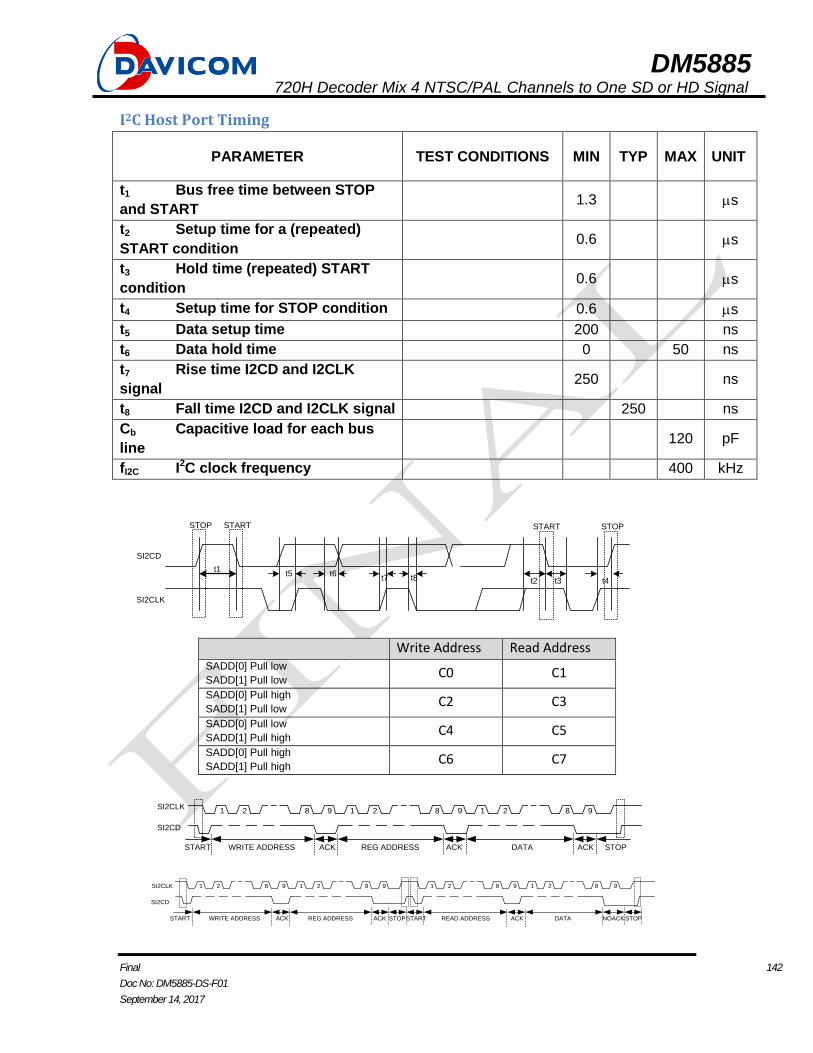
DM5885 720H Decoder Mix 4 NTSC/PAL Channels to One SD or HD Signal
Final 142
Doc No: DM5885-DS-F01
September 14, 2017
I2C Host Port Timing
PARAMETER TEST CONDITIONS MIN TYP MAX UNIT
t1 Bus free time between STOP
and START
1.3 s
t2 Setup time for a (repeated)
START condition
0.6 s
t3 Hold time (repeated) START
condition
0.6 s
t4 Setup time for STOP condition 0.6 s
t5 Data setup time 200 ns
t6 Data hold time 0 50 ns
t7 Rise time I2CD and I2CLK
signal
250 ns
t8 Fall time I2CD and I2CLK signal 250 ns
Cb Capacitive load for each bus
line
120 pF
fI2C I2C clock frequency 400 kHz
STARTSTOP START STOP
t1t7 t8
t5 t6t2 t3 t4
SI2CD
SI2CLK
Write Address Read Address SADD[0] Pull low
SADD[1] Pull low C0 C1
SADD[0] Pull high
SADD[1] Pull low C2 C3
SADD[0] Pull low
SADD[1] Pull high C4 C5
SADD[0] Pull high
SADD[1] Pull high C6 C7
1 2 8 9
ACK
1 2 8 9
ACKREG ADDRESS DATASTART ACK STOPWRITE ADDRESS
1 2 8 9SI2CLK
SI2CD
2 8 9 1 2 8 91 9
NOACKACKACK REG ADDRESS ACK DATA
8 9 1 2
READ ADDRESSSTART STARTSTOP STOP
1 2 8SI2CLK
SI2CD
WRITE ADDRESS
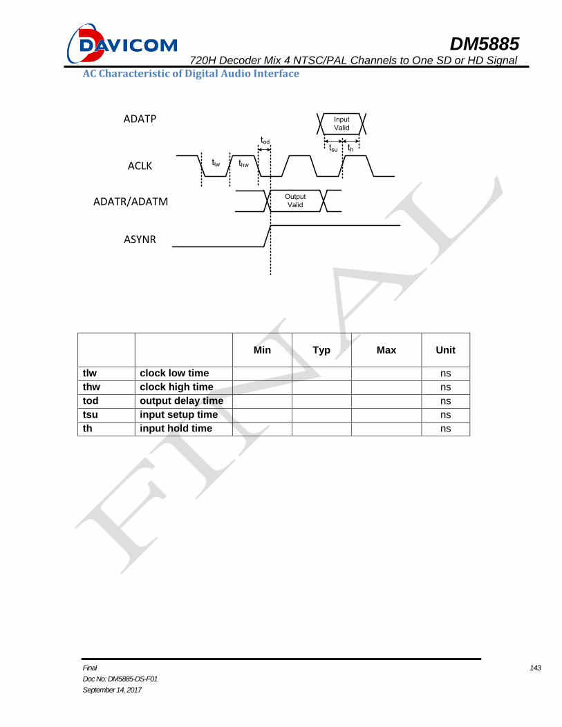
DM5885 720H Decoder Mix 4 NTSC/PAL Channels to One SD or HD Signal
Final 143
Doc No: DM5885-DS-F01
September 14, 2017
AC Characteristic of Digital Audio Interface
Output
Valid
ACLK
ADATR/ADATM
tsu th
thwtlw
ASYNR
ADATP Input
Valid
tod
Min Typ Max Unit
tlw clock low time ns
thw clock high time ns
tod output delay time ns
tsu input setup time ns
th input hold time ns
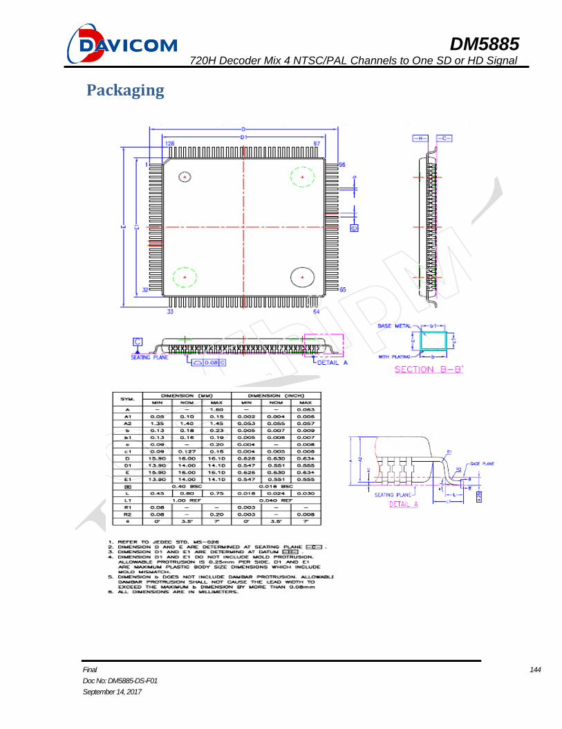
DM5885 720H Decoder Mix 4 NTSC/PAL Channels to One SD or HD Signal
Final 144
Doc No: DM5885-DS-F01
September 14, 2017
Packaging
DM5885 720H Decoder Mix 4 NTSC/PAL Channels to One SD or HD Signal
Final 145
Doc No: DM5885-DS-F01
September 14, 2017
Ordering Information Part Number Pin Count Package
DM5885EP 128
LQFP
(Pb-Free and
Halogen-Free)
Disclaimer The information appearing in this publication is
believed to be accurate. Integrated circuits sold by
DAVICOM Semiconductor are covered by the
warranty and patent indemnification provisions
stipulated in the terms of sale only. DAVICOM makes
no warranty, express, statutory, implied or by
description regarding the information in this
publication or regarding the information in this
publication or regarding the freedom of the described
chip(s) from patent infringement. FURTHER,
DAVICOM MAKES NO WARRANTY OF
MERCHANTABILITY OR FITNESS FOR ANY
PURPOSE. DAVICOM reserves the right to halt
production or alter the specifications and prices at
any time without notice. Accordingly, the reader is
cautioned to verify that the data sheets and other
information in this publication are current before
placing orders. Products described herein are
intended for use in normal commercial applications.
Applications involving unusual environmental or
reliability requirements, e.g. military equipment or
medical life support equipment, are specifically not
recommended without additional processing by
DAVICOM for such applications. Please note that
application circuits illustrated in this document are for
reference purposes only.
DAVICOM’s terms and conditions printed on the
order acknowledgment govern all sales by DAVICOM.
DAVICOM will not be bound by any terms
inconsistent with these unless DAVICOM agrees
otherwise in writing. Acceptance of the buyer’s orders
shall be based on these terms.
Company Overview DAVICOM Semiconductor Inc. develops and
manufactures integrated circuits for integration into
data communication products. Our mission is to
design and produce IC products that are the
industry’s best value for Data, Audio, Video, and
Internet/Intranet applications. To achieve this goal,
we have built an organization that is able to develop
chipsets in response to the evolving technology
requirements of our customers while still delivering
products that meet their cost requirements.
Products We offer only products that satisfy high performance
requirements and which are compatible with major
hardware and software standards. Our currently
available and soon to be released products are based
on our proprietary designs and deliver high quality,
high performance chipsets that comply with modem
communication standards and Ethernet networking
standards.
Contact Windows For additional information about DAVICOM products, contact the Sales department at:
Headquarters
Hsin-chu Office: No.6 Li-Hsin Rd. VI, Science-based Industrial Park, Hsin-chu City, Taiwan, R.O.C. TEL: +886-3-5798797
FAX: +886-3-5646929
MAIL: [email protected]
HTTP: http://www.davicom.com.tw
WARNING Conditions beyond those listed for the absolute maximum may destroy or damage the products. In addition, conditions for sustained periods at near the limits of the operating ranges will stress and may temporarily (and permanently) affect and damage structure, performance and function.

![PVCPR11 Edital 3.5 GHz v03.ppt [Modo de Compatibilidade]...2011/06/09 · 35 MHz 35 MHz 10 MHz 10 MHz 10 MHz 10 MHz 10 MHz 10 MHz 3.400,00 MHz 3.600,00 MHz 10 MHz 35 MHz 10 MHz 10](https://img.pdfslide.tips/doc/110x75/5f7286506e7f433bb4685297/pvcpr11-edital-35-ghz-v03ppt-modo-de-compatibilidade-20110609-35-mhz.jpg)