Embed Size (px)
Citation preview
DPD/ETPA/RFIC, Multi - port device test for
Intelligent device
1
Keven Chang 張啟文 Module Specialist

Agenda
1. Key Intelligent Device Challenges
2. Technology Overview
3. Measurement Considerations
4. Measurement Architectures & Solutions
5. Q&A
2
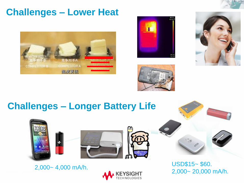
Challenges – Lower Heat
08-May-12
Modular Solutions Presentation
3
Challenges – Longer Battery Life
USD$15~ $60.
2,000~ 20,000 mA/h. 2,000~ 4,000 mA/h.

Challenges – Lower Size ? & Testing Cost
08-May-12
Modular Solutions Presentation
4
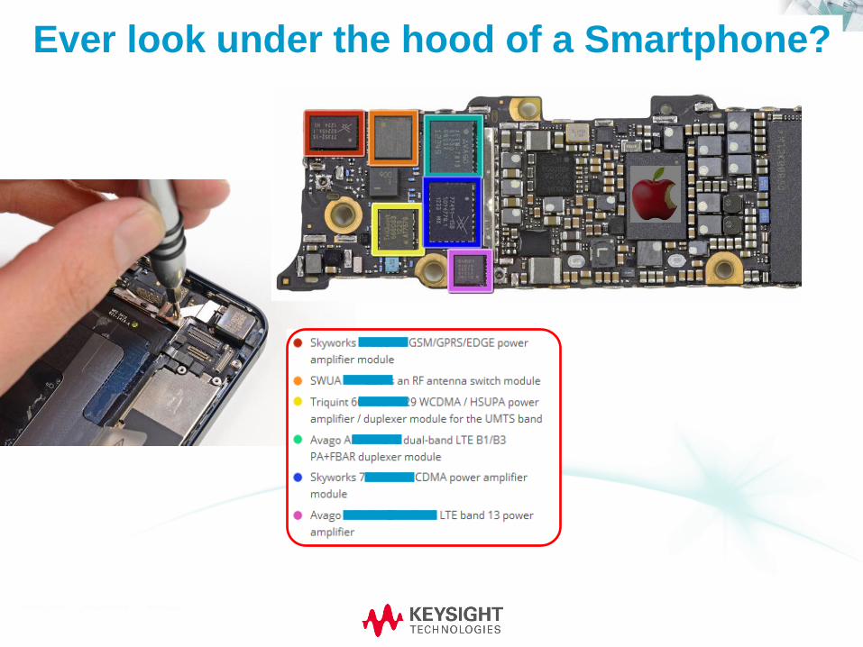
Ever look under the hood of a Smartphone?

Agenda
1. Key Intelligent Device Challenges
2. Technology Overview
3. Measurement Considerations
4. Measurement Architectures & Solutions
5. Q&A
6

Digital Pre-Distortion (DPD) Why & How
Modern communication systems
• Signals have high peak-to-average power ratios (PAPR).
• Must operate with high power-added efficiency (PAE).
High PAPR is a consequence of high spectral efficiency
• Multiple-Carrier Signals (MC GSM, MC WCDMA)
• CDMA (WCDMA, CDMA2000)
• OFDM (LTE, WiMAX)
High PAE is achieved when the RF power amplifier (PA) is driven towards saturation
Operation near saturation inherently results in higher signal distortion
Maximum
correctable
power
Psat
INPUT
POWER
OUTPUT
POWER
LINEAR
REGION
DPD
REGION
LINEARIZED
DPD + PA
PA, WITH GAIN
COMPRESSION
DPD GAIN
EXPANSION
+ =
7
DPD corrects PA nonlinearities resulting in higher performing power amplifiers

DPD Architecture and Bandwidth Requirement
Digital
Pre-
Distortion
RF
Up-converter Coupler PA
DPD
Extraction
and Control
RF Down-
Converter &
Digitizer
3-5 x BW 3-5 x BW 3-5 x BW
3-5 x BW 3-5 x BW
Sample rate must be 3-5 x the BW of the RF signal
7/3/2014
Techniques to Reduce Characterization Test
Times of PAD Devices 8
Before DPD After DPD
Poor EVM Good EVM
Poor ACP Good ACP
Volterra Series Adaptive Process
Memory Polynomial Process
LUT Adaptive process

Dynamic EVM The Why & How
A Simplified Envelope Tracking Technique
Used for Wireless LAN
• Device is turned off between packets
to conserve power
• Testing must ensure device turns on & off
quickly without negative transient or
thermal effects
Dynamic EVM test method
• Square wave pulse applied to PA enable
(during RF burst)
Test equipment same as
for envelope tracking
9
Wireless LAN Brust Signal
PA ON/OFF Signal Time advance (Before & After)
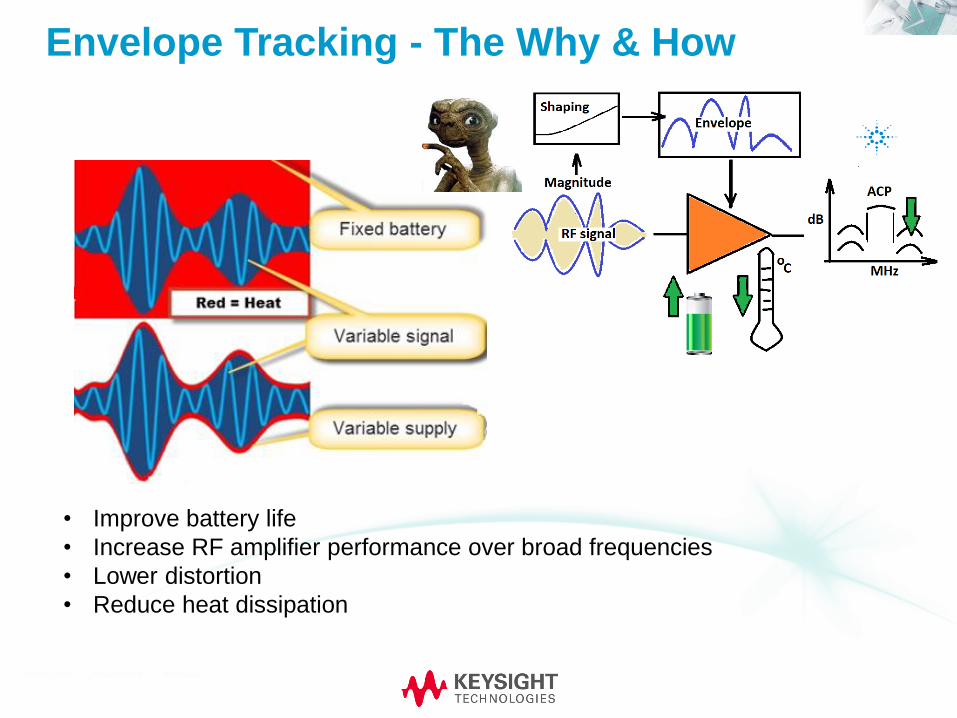
• Improve battery life
• Increase RF amplifier performance over broad frequencies
• Lower distortion
• Reduce heat dissipation
Envelope Tracking - The Why & How
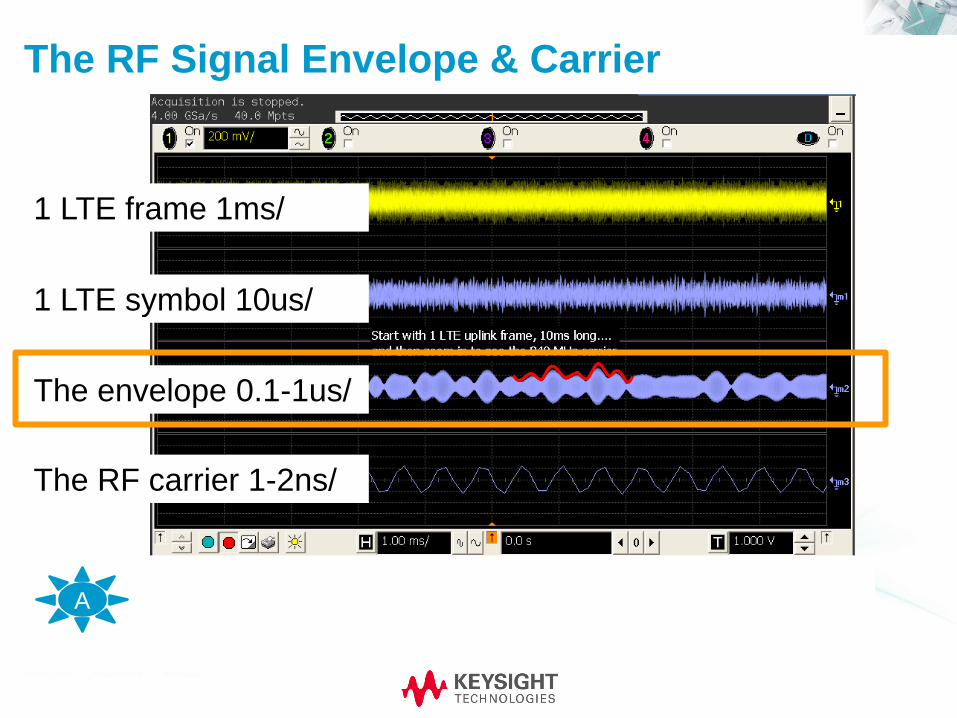
The RF Signal Envelope & Carrier
1 LTE symbol 10us/
1 LTE frame 1ms/
The envelope 0.1-1us/
The RF carrier 1-2ns/
A

The Evolution of a Handset PA
Techniques to Reduce Characterization Test
Times of PAD Devices 12

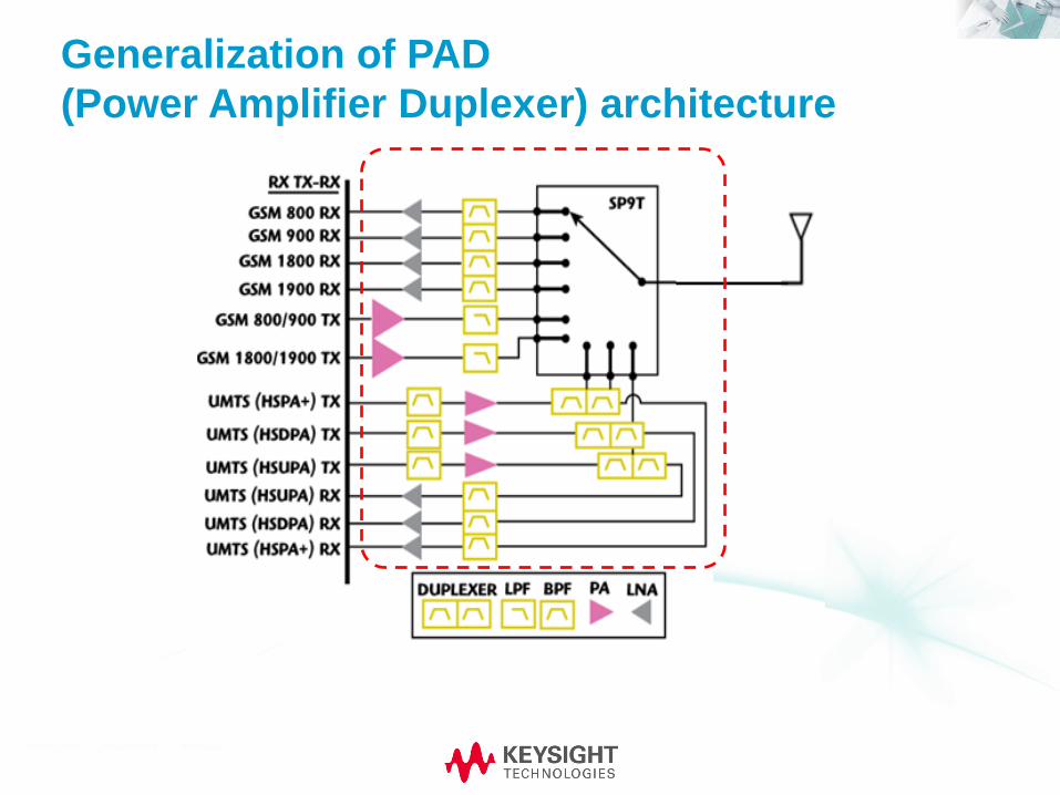
Generalization of PAD
(Power Amplifier Duplexer) architecture
Techniques to Reduce Characterization Test
Times of PAD Devices 13
Filters &
Duplexer
Antenna
Switch
RF
Transceiver
PA
DC Supply
DC Modulator
MIPI
RFFE
Device Control
Filters &
Duplexer
Filters &
Duplexer
PA
Rx
Rx
Rx
IQ Envelope
Mode
Switch

Agenda
1. Key Intelligent Device Challenges
2. Technology Overview
3. Measurement Considerations
4. Measurement Architectures & Solutions
5. Q&A
14

Review – ACPR Adjacent Channel Power (Leackage) Ratio (ACLR)
08-May-12
Modular Solutions Presentation
15
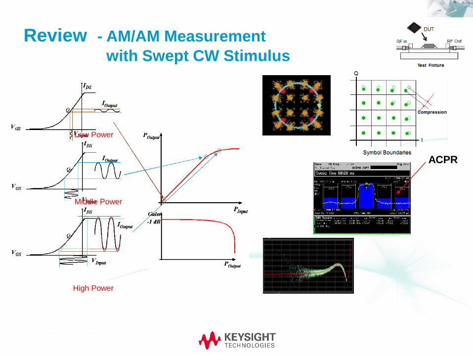
Review - AM/AM Measurement
with Swept CW Stimulus
Low Power
Middle Power
High Power
ACPR
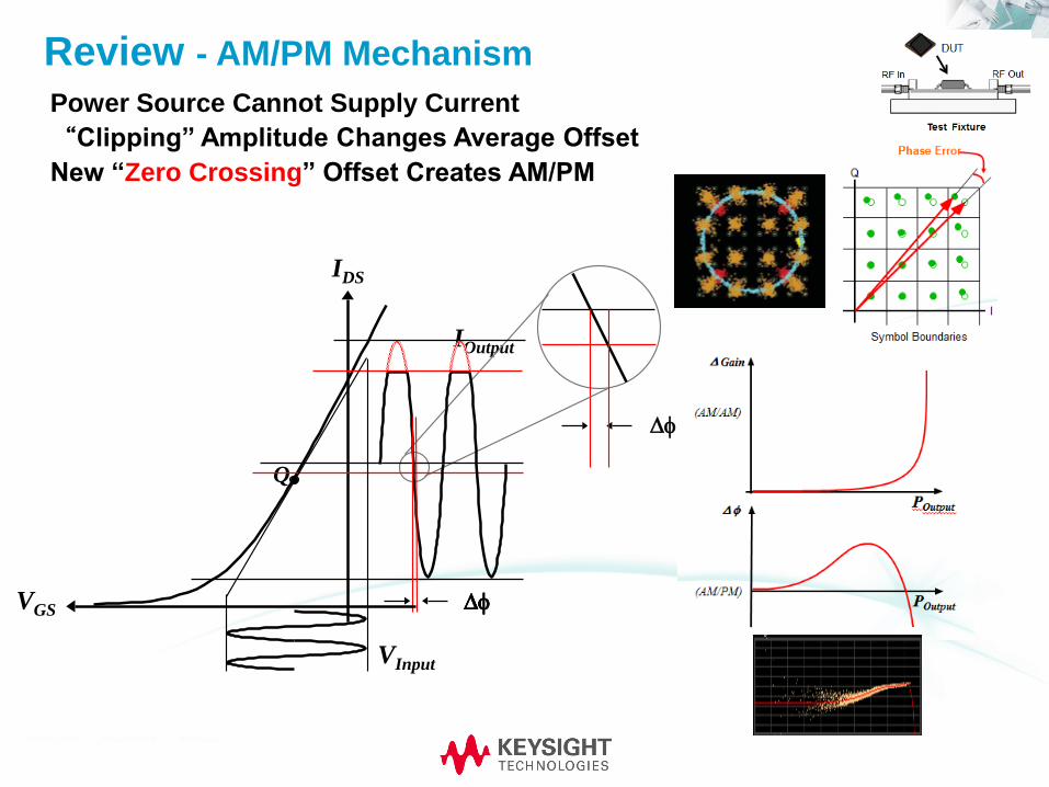
Review - AM/PM Mechanism
Power Source Cannot Supply Current
“Clipping” Amplitude Changes Average Offset
New “Zero Crossing” Offset Creates AM/PM
Q
VInput
VGS
IDS
IOutput
Df
Df Df

Review - PAE (Power Added Efficiency)
PA
E
RF output voltage
PAE ~ RF Pout
Supply Pin
100%
50-60%
at peak
output
What you want
What we expected!
Power
Added
Efficiency

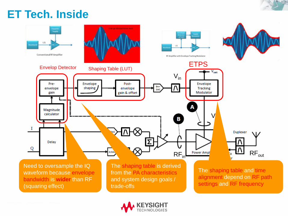
ET Tech. Inside
08-May-12
Modular Solutions Presentation
19
08-May-12
Modular Solutions Presentation
20
ET Tech. Inside
ETPS Envelop Detector Shaping Table (LUT)
Vcc
RFout RFin
Vin
Need to oversample the IQ
waveform because envelope
bandwidth is wider than RF
(squaring effect)
The shaping table is derived
from the PA characteristics
and system design goals /
trade-offs
The shaping table and time
alignment depend on RF path
settings and RF frequency
PA
Supply
voltage
RF output voltage
• Supply does not go to 0V
• PA operating in linear range
• PA input determines output
performance
• Smooth transition controls
envelope bandwidth
• Voltage may not be limited
• Higher peak voltage extends
PA operating range
• PA in compression
• Supply determines PA output
amplitude
• Curve sets PA amplitude
linearity and efficiency
• Supply does not go to 0V
• PA operating in linear range
• PA input signal largely
determines output distortion
• Voltage not always clipped
• Clipping gives simple CFR
• Higher peak voltage extends
PA operating range
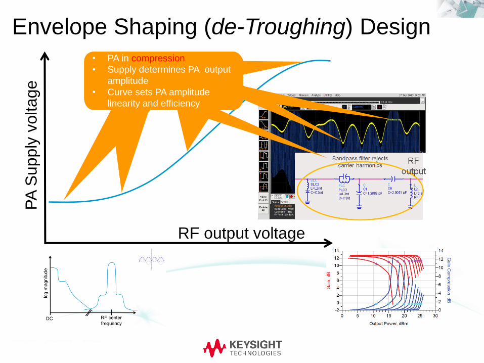
Envelope Shaping (de-Troughing) Design
• PA in compression
• Supply determines PA output
amplitude
• Curve sets PA amplitude
linearity and efficiency

A
RF spectrum The main power
content has the same
bandwidth as the RF log m
agnitude
RF center
frequency DC
Constant scaling
(MHz / div)
Distortion
(ACP)
DC
component
The Envelope Spectrum & How to Control It
The roll off
depends on use of
shaping curve to
minimize sharp
signal transitions
Envelope
spectrum
The roll off
depends on use of
shaping curve to
minimize sharp
signal transitions

ET PA takes
less power
+23 dBm PA output
Yes - Reduction in Average Power

ET PA, ETPS & System Analysis
Linearity & time alignment Mixed RF & Baseband
24

Does ET work? Fixed supply

Does ET work? Tracking supply
PA operating in ET
mode has less
distortion
PA operating in ET
mode has less
distortion
PA operating in ET
mode has less
distortion
PA operating in ET
mode has less
distortion
A

08-May-12
Modular Solutions Presentation
27
Timing Misalignment

Timing Misalignment Causes ACP Variation
28
5 MHz LTE 25RB 1ns steps
A
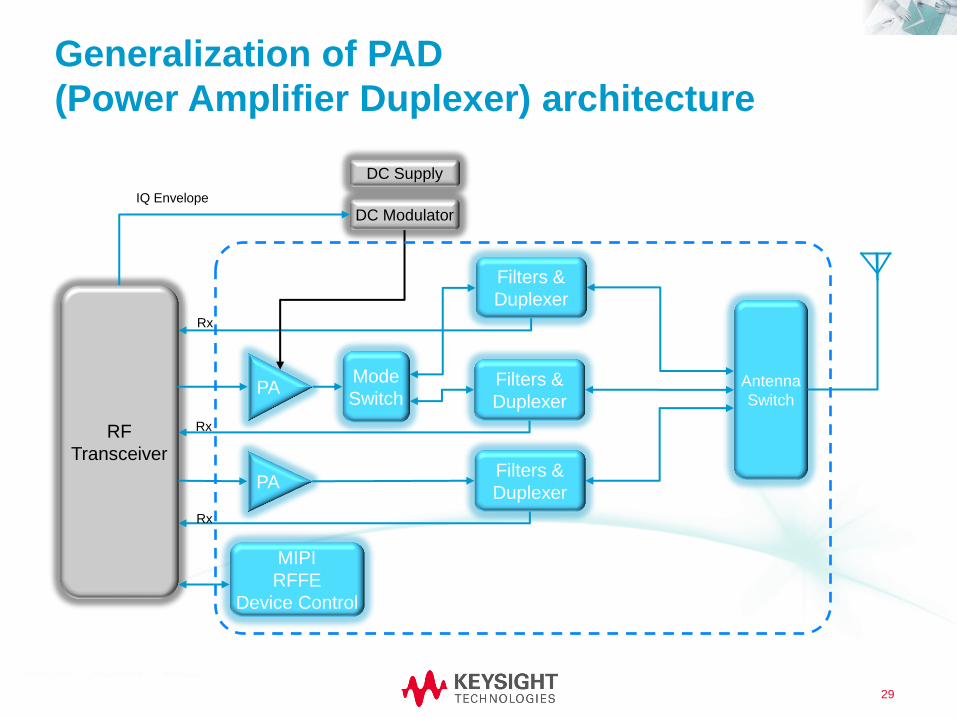
Generalization of PAD
(Power Amplifier Duplexer) architecture
Techniques to Reduce Characterization Test
Times of PAD Devices 29
Filters &
Duplexer
Antenna
Switch
RF
Transceiver
PA
DC Supply
DC Modulator
MIPI
RFFE
Device Control
Filters &
Duplexer
Filters &
Duplexer
PA
Rx
Rx
Rx
IQ Envelope
Mode
Switch
Generalization of PAD
(Power Amplifier Duplexer) architecture
08-May-12
Modular Solutions Presentation
31
Generalization of PAD
(Power Amplifier Duplexer) architecture
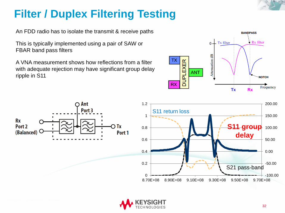
Filter / Duplex Filtering Testing
An FDD radio has to isolate the transmit & receive paths
This is typically implemented using a pair of SAW or
FBAR band pass filters
A VNA measurement shows how reflections from a filter
with adequate rejection may have significant group delay
ripple in S11
-100.00
-50.00
0.00
50.00
100.00
150.00
200.00
0
0.2
0.4
0.6
0.8
1
1.2
8.70E+08 8.90E+08 9.10E+08 9.30E+08 9.50E+08 9.70E+08
S11 group
delay
S21 pass-band
S11 return loss
Techniques to Reduce Characterization Test
Times of PAD Devices 32

Agenda
1. Key PA Challenges & Technology
2. ET Measurement Considerations
3. Measurement Architectures & Solutions
4. Q&A
33

Power Amplifier Test Solutions
34
• PA Testing Solutions Across Product Delivery
Design Verification Production
LXI
Benchtop
PXI
Modular

ETPA (Envelop Tracking Power Amplify)
Benchtop Solutions for R&D and DVT
35
RF Out RF In
Vcc Vbat
RFFE
PA
ETPS
ET Waveform
I/Q Waveform
AWG: 33522B
Proprietary
Control
Trigger V.. V..
SystemVue , Simulation s/w
Generated Waveforms
Signal Generation
s/w
or
DC Power Analyzer
N7605B
VSA
VSG : M5182A
DSO9000
VSA s/w
High performance,
low cost envelope
generation
Time alignment & linearity
(AM/AM, AM/PM, Gain
compression)
Waveform creation
includes shaped envelope
& envelope download
Soltuions
AM/AM
AM/PM
Gain Compression
PAE
ACLR
Delta EVM
Dynamic EVM
Shaping Table
Example:
Scout RFFE
USB Dongle
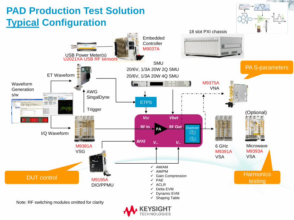
PAD Production Test Solution
Typical Configuration
36
RF Out RF In
Vcc Vbat
V.. RFFE V..
PA
ET Waveform
I/Q Waveform
M9381A
VSG
6 GHz
M9391A
VSA
AWG
SingalDyne
Trigger
ETPS
USB Power Meter(s)
Waveform
Generation
s/w
Harmonics
testing
Embedded
Controller
M9037A
18 slot PXI chassis
Note: RF switching modules omitted for clarity
PA S-parameters
DUT control
(Optional)
Microwave
M9393A
VSA
M9375A
VNA
M9195A
DIO/PPMU
SMU
AM/AM
AM/PM
Gain Compression
PAE
ACLR
Delta EVM
Dynamic EVM
Shaping Table
20/6V, 1/3A 20W 4Q SMU
20/6V, 1/3A 20W 2Q SMU
U2021XA USB RF sensors
Duplexer
Ready to Go Measure
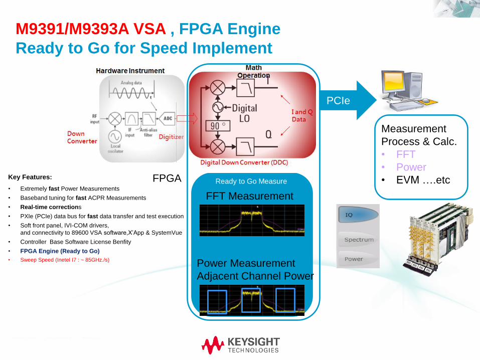
M9391/M9393A VSA , FPGA Engine
Ready to Go for Speed Implement
FPGA
PCIe
FFT Measurement
Power Measurement
Adjacent Channel Power
Measurement
Process & Calc.
• FFT
• Power
• EVM ….etc Key Features:
• Extremely fast Power Measurements
• Baseband tuning for fast ACPR Measurements
• Real-time corrections
• PXIe (PCIe) data bus for fast data transfer and test execution
• Soft front panel, IVI-COM drivers,
and connectivity to 89600 VSA software,X’App & SystemVue
• Controller Base Software License Benfity
• FPGA Engine (Ready to Go)
• Sweep Speed (Inetel I7 : ~ 85GHz./s)

M9381A VSG
38
RF/MW
DAC
DAC
LPF
Q
90 LO
I
I/Q
Waveform
File
16 Q RAM
16
16
16 I RAM
I/Q modulator (Up Converter)
LPF
ALC 16
16
Baseband Generator
160
MS/s
Q
90 LO
I
Baseband Frequency and Amplitude Offset
with the M9381A Vector Signal Generator
160
MHz
20 dB
< 200 us
• Signal Processing ASIC in baseband generator supports changing Frequency and Amplitude of RF Signal
without Adjusting Analog Hardware (fastune technology innovation)
• Power Servo Loop Approach:
• Set the “RF Power Level” to the maximum level that may be required from the source
• Use the “baseband power level” to adjust the power level to the required input level
• <200 us amplitude changes using command interface ,<10us (List Mode)
M937x Multiport VNA
Measurements for PA , Duplexer , Switch
Multiple M937xA VNAs in PXI
For best performance, you need:
• True multiport VNA with independent modules
• Improved throughput
• High fidelity measurements without needing
external port switches
• Full N-port correction
Techniques to Reduce Characterization Test
Times of PAD Devices 39
Filters &
Duplexer
Antenna
Switch
RF
Transceiver
PA
DC Supply
DC Modulator
MIPI
RFFE
Device Control
Filters &
Duplexer
Filters &
Duplexer
PA
Rx
Rx
Rx
IQ Envelope
Mode
Switch

M937x PXI VNA
40
Options
010 : Time domain
551 : N-port calibrated measurement
102 : Additional VNA features and capabilities
Fixture simulator Manual & automated port extend & Equation editor
897 : Built-in performance test software for inclusive calibration
898 : Built-in performance test software for standards compliant calibration
32-port True Crossbar 26.5 GHz VNA in 4U Chassis

M937X PXI VNA Performance
41
8
16
24
Nu
mb
er
of p
ort
s o
n D
UT
Number of sweeps for an N-port measurement
100 200 300 400 500 0
56
8
240
112
16
552
264
24
24
M937xA with 24-ports
4-port Switch Matrix VNA
2-port Switch Matrix VNA
Cycle Time
M9372A
8753ES 848 msec
57 msec
1,601 pts, full 2-p cal, small span
IFBW = 6 kHz (8753ES), 500 kHz (E5071C) 600 kHz (M9372A)
x15 faster
E5071C 41 msec
Trace Noise Dynamic Range
IFBW = 10 Hz,
Max specified power
The same quality results you have
come to expect in our VNA

Keysight Phase 2 (2014.Sept. 15th)
Reference Solution Block Diagram
Drivers
Device Under Test Hardware Software Application
Target Market - RF PA production test
- RF PA DVT with ET/DPD test
Description - High Speed ET, DPD
- > 6 GHz Harmonics
- Multi-port VNA
New features - Agilent modules : VNA, M9393A VSA
- 3rd party modules : AWG
- Software : Signal Studio for RF PA
PXI VSG
ETPS
Reference
Solution Libraries
X-Apps
Signal
Studio for RF PA
+ LTE
Reference
Solution
GUI
PXI VSA
Customer
Test
Applicatio
n
RF PA
RFFE
PXI VNA
LXI SMU
USB DIO
Duplexer
eFTD Sept 2014
PXI AWG Signadyne

08-May-12
Modular Solutions Presentation
43

M9451A FPGA DPD PXIe Measurement Accelerator
08-May-12
Modular Solutions Presentation
44
M9451A DPD FPGA speeds up DPD/ET test applications Key features include:
Digital Pre-Distortion
– Open or closed loop
– PA optimization techniques: Look up table (LUT)
– Fast peer-to-peer (P2P) data transfer to/from PXI signal generator and signal
analyzer
Envelope Tracking
– Hardware accelerated envelope tracking waveform generation
– Fast data transfer to arbitrary waveform generator (AWG
M9451A Digital Pre-Distortion and Envelope Tracking Block Diagram

PA Test Reference Solution Phase 3 - Resource Manager, X’App , SFP IVI Measure
- Application WCDMA,CDMA2K,EVDO,TD-SCDMA,LTE,WLAN
- Testing Item
- Power Servo
- DC Current
- ACPR
- EVM
- Harmonic
- SEM
- ETPA
- DPD
- DC: SMU
- ET : ARB
- RFFE
- Power Sensor
- Calibration
-Speed Performance.

08-May-12
Modular Solutions Presentation
46
M9381A VSG Key Features:
• Frequency range: 1 MHz to 3 or 6 GHz (options)
• Modulation bandwidth: 40, 100, 160 MHz (options)
• Phase Noise (10 kHz offset @ 1GHz carrier) -125 dBc/Hz typical
• Frequency Settling Time to within 1kHz <220 us
• <10 us utilizing baseband tuning within modulation BW (+/-80 MHz)
• Amplitude Settling Time <120 us
• <10 us for changes 0 to 20 dB utilizing baseband tuning within modulation BW (+/-80 MHz)
• RF Flatness Corrected <0.4 dB (140 MHz BW)
• Min/Max Output power -120dBm (Specified, settable to -130 dBm) /+19dBm
• Real-time corrections
• Generator Memory 1024 MSa
• PXIe (PCIe) data bus for fast data transfer and test execution
M9393A VSA Key Features
• 9KHz~8.4/14/18/27 GHz (upgradeable Solftware Options)
• 40/100/160 MHz Bandwidth (upgradeable Solftware Options)
• ~ 150 us Frequency Tuning
• ~ 10 us Amplitude Switching
• +/- 0.15 dB Amplitude Accuracy across frequency and temperature
• Connectivity to 89600 VSA, Modular X-Apps, Modular spectrum application
• Power Spectral Engine for fast spectrum capture (FFT-based)
• 27GHz. Sweep ~ 1 Second (RBW: 10KHz)
M9391A VSA Key Features:
• Frequency range: 1 MHz to 3 or 6 GHz (options)
• Analysis bandwidth: 40, 100, 160 MHz (options)
• Absolute amplitude accuracy ±0.7 dB to 3 GHz, and ±0.9 dB to 6 GHz
• TOI +23 dBm
• Displayed average noise level -140dBm/Hz (-156dBm/Hz with PreAmp)
• WCDMA ACLR Dynamic Range -68 dBc
• Real-time Power Measurements
• Baseband tuning for Fast ACPR Measurements
• Real-time corrections
• PXIe (PCIe) data bus for fast data transfer and test execution
PXI Hardware Reference

08-May-12
Modular Solutions Presentation
47
M9195A DSR Key Features & Specifications
16 per pin programmable channels for logic levels, delay
Parametric Measurement Unit (PMU) per channel
Single and multi-site configurability
Flexible per bit timing control
On-the-fly pattern generation and editing
Allocation of deep pattern memory per channel
High voltage drivers and open drain control pins
Software tools for quick test development
M937xA PXI VNA Key Features & Specifications
Full 2-port S-parameters in a single-slot module
N-port multiport configurations available with multiple modules
Configurable as multiple independent VNAs
Compatible with electronic calibration (ECal) modules
Test multiple devices simultaneously, with multi-VNA capability
Test multiport devices faster than using switch matrices
The fastest measurement speed in a PXI VNA
Best accuracy derived from the best PXI VNA specifications
Fast sweep speed: 18 msec, 401 points, 600 kHz IFBW
Dynamic range: 95 dB specified at 24 GHz, 65 dB typical at 26.5 GHz
Trace noise: 0.006 dB at 24 GHz, 0.020 dB at 26.5 GHz
Stability: ± 0.020 dB/ºC
PXI Hardware Reference
M9451A DPD FPGA speeds up DPD/ET test applications Key features include:
Digital Pre-Distortion
– Open or closed loop
– PA optimization techniques: Look up table (LUT)
– Fast peer-to-peer (P2P) data transfer to/from PXI signal generator and signal
analyzer
Envelope Tracking
– Hardware accelerated envelope tracking waveform generation
– Fast data transfer to arbitrary waveform generator (AWG
08-May-12
Modular Solutions Presentation
48
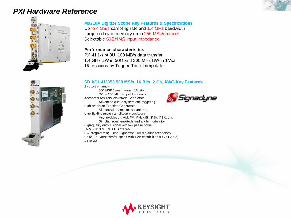
M9210A Digitize Scope Key Features & Specifications
Up to 4 GS/s sampling rate and 1.4 GHz bandwidth
Large on-board memory up to 256 MSa/channel
Selectable 50Ω/1MΩ input impedance
Performance characteristics
PXI-H 1-slot 3U, 100 MB/s data transfer
1.4 GHz BW in 50Ω and 300 MHz BW in 1MΩ
15 ps accuracy Trigger-Time-Interpolator
SD AOU-H3353 500 MS/s, 16 Bits, 2 Ch, AWG Key Features 2 output channels
500 MSPS per channel, 16 bits
DC to 200 MHz output frequency
Advanced Arbitrary Waveform Generators
Advanced queue system and triggering
High-precision Function Generators
Sinusoidal, triangular, square, etc.
Ultra-flexible angle / amplitude modulators
Any modulation: AM, FM, PM, ASK, FSK, PSK, etc.
Simultaneous amplitude and angle modulation
High-quality output signal with low phase noise
16 MB, 128 MB or 1 GB of RAM
HW programming using Signadyne HVI real-time technology
Up to 1.6 GB/s transfer speed with P2P capabilities (PCIe Gen 2)
1 slot 3U
PXI Hardware Reference
Summary
49
ET is fast becoming an important capability for PA’s supporting linear modulation schemes
ET provides: Improved PA efficiency Lower distortion Broader frequency coverage Longer handset battery life
ET measurements and characterization can be challenging Agilent Technologies can provide the needed hardware and
software needed for ET systems testing from R&D through DVT to Production test

Reference Material
50
www.agilent.com/find/envelope_tracking
• Envelope tracking solution guide
• Videos: ET signal generation and analysis
• App Note: Simulating ET in ADS
• Article: X-parameter models for an RF PA using ET
EEsof RF Power Amplifier Design Webcast Series
• Part 5: Envelope Tracking Simulation and Analysis

Questions
51
Additional Reading:
OpenET Alliance
Simulation and X-parameter Models for PA’s with ET
Envelope Tracking Simulation and Analysis
![DAMAGE CONTROL (DC) - dcfpnavymil.org Damage Control (DC) [1].pdf201 Damage Control (DC) Communications-----59 202 Emergency Escape Breathing Device (EEBD ... 210 Aqueous Film Forming](https://img.pdfslide.tips/doc/110x75/5ac86b917f8b9a40728cbe54/damage-control-dc-damage-control-dc-1pdf201-damage-control-dc-communications-59.jpg)