Embed Size (px)
Citation preview
Effects of Triphenylborane Addition to Decaphenylcyclopentasilane Thin Films
Takeo Oku1*, Naoki Hibi1, Atsushi Suzuki1, Tsuyoshi Akiyama1, Masahiro Yamada2, Sakiko Fukunishi3 and Kazufumi Kohno3
1Department of Materials Science, The University of Shiga Prefecture, Shiga 522-8533,
Japan 2Osaka Gas Co., Ltd., Osaka 554-0051, Japan 3Osaka Gas Chemicals Co., Ltd., Osaka 554-0051, Japan
E-mail: [email protected]
(Received July 18, 2014)
Organic thin film solar cells are potential ‘next generation’ solar cells. Many p-type
semiconductors have been used in organic solar cells, but there have been far fewer reports
involving n-type organic semiconductors. Developing new n-type organic semiconductors is
therefore desirable. Decaphenylpentasilane (DPPS) thin films were spin-coated from solutions
containing boron (B), and the effects of B addition on film microstructures and electronic
properties were investigated. Microstructures of DPPS thin films were investigated by X-ray
diffraction, and DPPS thin films doped with B (DPPS(B)) showed the reduction of crystallinity
upon annealing at 300 °C, while DPPS thin films exhibited crystalline structures. DPPS(B) thin
films exhibited decreased electrical resistances upon the B doping and annealing. The desorption
of phenyl and methyl groups from the DPPS(B) thin films was observed by Raman scattering
measurements.
1. Introduction
Polysilanes are a p-type semiconductor, and have been applied as electronic conductive materials
and photovoltaic systems [1-11]. Polysilanes are organic polymers containing main chain Si-Si
bonds and side chain organic substituents, which are known as σ-conjugate polymers, and their
hole mobility is ~10–4 cm2 V–1 s–1 [1]. Although the polysilanes could be applied as a p-type
semiconductor on organic thin film solar cells for these characteristics, few studies on polysilane
solar cells have been reported. Doped polysilanes as an n-type semiconductor have been developed
and applied for organic solar cells [11,12].
The purpose of the present work is to prepare decaphenylcyclopentasilane thin films using
spin-coating mixture solutions of decaphenylpentasilane (DPPS) with triphenyl borane, and to
evaluate the effect of boron (B) and annealing temperatures on their electronic properties and
microstructures. It is expected that amorphous silicon doped with boron would function as a p-type
semiconductor. Spin-coating is a low-cost method, and is essential for mass production of solar
cells [13]. Optical property and desorption of phenyl group were investigated from
ultraviolet-visible (UV-vis) absorption and Raman scattering spectra. Microstructure analysis was
carried out by X-ray diffraction (XRD) analysis. The mechanism of microstructural change is
discussed on the basis of the experimental results.
2. Experimental
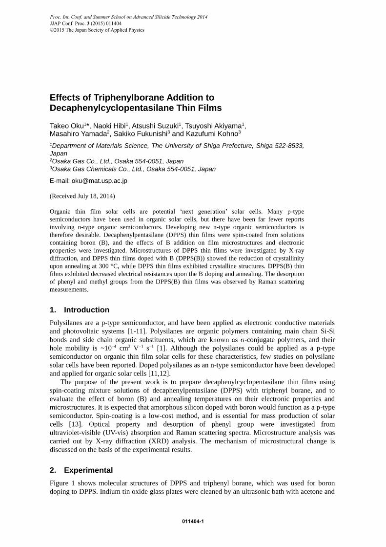
Figure 1 shows molecular structures of DPPS and triphenyl borane, which was used for boron
doping to DPPS. Indium tin oxide glass plates were cleaned by an ultrasonic bath with acetone and
JJAP Conf. Proc. (2015) 011404©2015 The Japan Society of Applied Physics
3Proc. Int. Conf. and Summer School on Advanced Silicide Technology 2014
011404-1
methanol, and then were dried with nitrogen gas. The triphenylborane and DPPS were mixed in 1
mL tetrahydrofuran. The mixed solution was spin-coated at 1000 rpm, and then annealed at
100~300 °C. Gold contacts were evaporated as a top electrode by vacuum deposition to measure
the electrical resistance of the film. The current density–voltage characteristics (Hokuto Denko
HSV-110) of the devices were measured to investigate the electrical resistances of the films. The
microstructures of the DPPS thin films were investigated by XRD analysis (Philips X’Pert-MPD
System) with CuKα radiation at 40 kV operating voltage and 40 mA operating current. Raman
scattering spectra were recorded with a laser Raman spectrometer (Jasco NRS-5100). The Raman
scattering spectra and optical images of the thin films after annealing were observed using an
excitation laser with a wavelength at 532 nm. Optical properties were investigated by UV-vis
absorption spectroscopy (Jasco, V-670). The molecular structures of the DPPS monomers were
optimized by ab-initio calculation based on the density functional theory using Gaussian 09. The
active modes in Raman scattering spectra were calculated by DFT/B3LYP/6-31G in the frequency
mode.
Fig. 1. Structures of (a) DPPS and (b) triphenylborane.
3. Results and Discussion
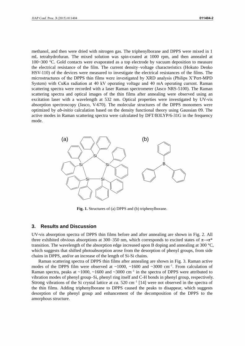
UV-vis absorption spectra of DPPS thin films before and after annealing are shown in Fig. 2. All
three exhibited obvious absorptions at 300–350 nm, which corresponds to excited states of π→π*
transition. The wavelength of the absorption edge increased upon B doping and annealing at 300 °C,
which suggests that shifted photoabsorption arose from the desorption of phenyl groups, from side
chains in DPPS, and/or an increase of the length of Si-Si chains.
Raman scattering spectra of DPPS thin films after annealing are shown in Fig. 3. Raman active
modes of the DPPS film were observed at ~1000, ~1600 and ~3000 cm–1. From calculation of
Raman spectra, peaks at ~1000, ~1600 and ~3000 cm–1 in the spectra of DPPS were attributed to
vibration modes of phenyl group–Si, phenyl ring itself and C-H bonds in phenyl group, respectively.
Strong vibrations of the Si crystal lattice at ca. 520 cm–1 [14] were not observed in the spectra of
the thin films. Adding triphenylborane to DPPS caused the peaks to disappear, which suggests
desorption of the phenyl group and enhancement of the decomposition of the DPPS to the
amorphous structure.
Si Si
Si
Si
Si B
(a) (b)
011404-2JJAP Conf. Proc. (2015) 0114043
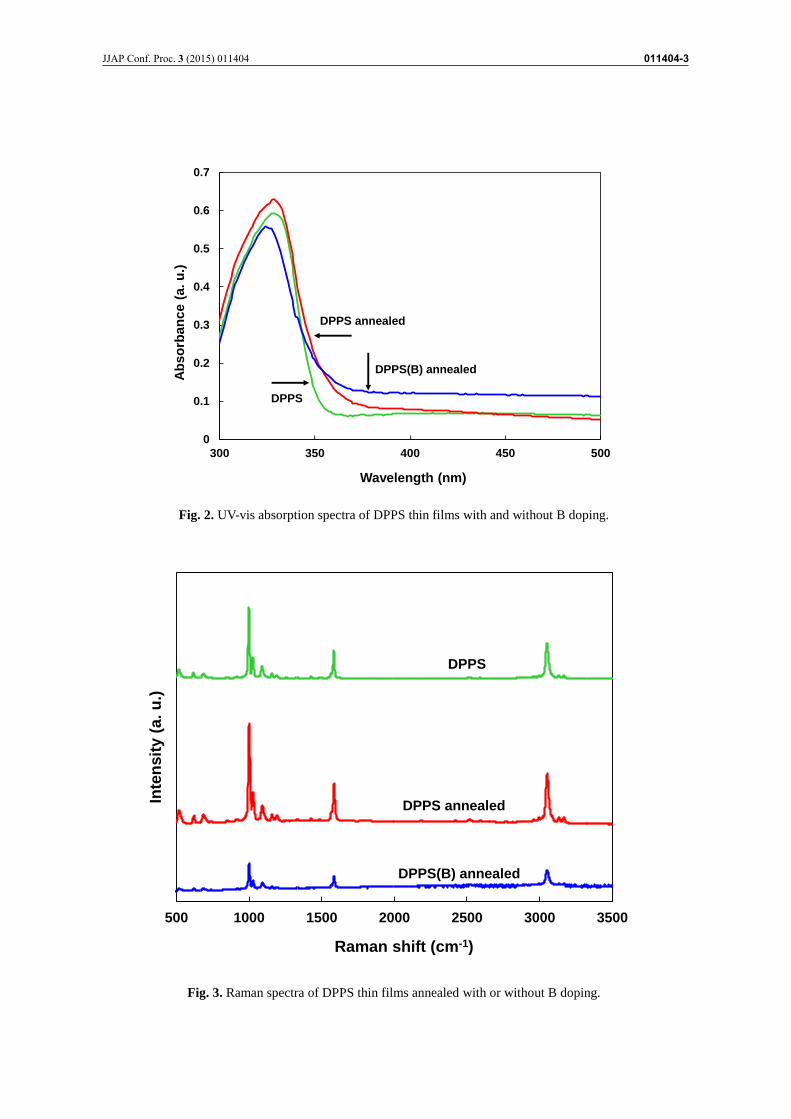
Fig. 2. UV-vis absorption spectra of DPPS thin films with and without B doping.
Fig. 3. Raman spectra of DPPS thin films annealed with or without B doping.
0
0.1
0.2
0.3
0.4
0.5
0.6
0.7
300 350 400 450 500
Ab
so
rban
ce (
a. u
.)
Wavelength (nm)
DPPS
DPPS(B) annealed
DPPS annealed
500 1000 1500 2000 2500 3000 3500
Inte
nsit
y (
a.
u.)
Raman shift (cm-1)
DPPS
DPPS(B) annealed
DPPS annealed
011404-3JJAP Conf. Proc. (2015) 0114043
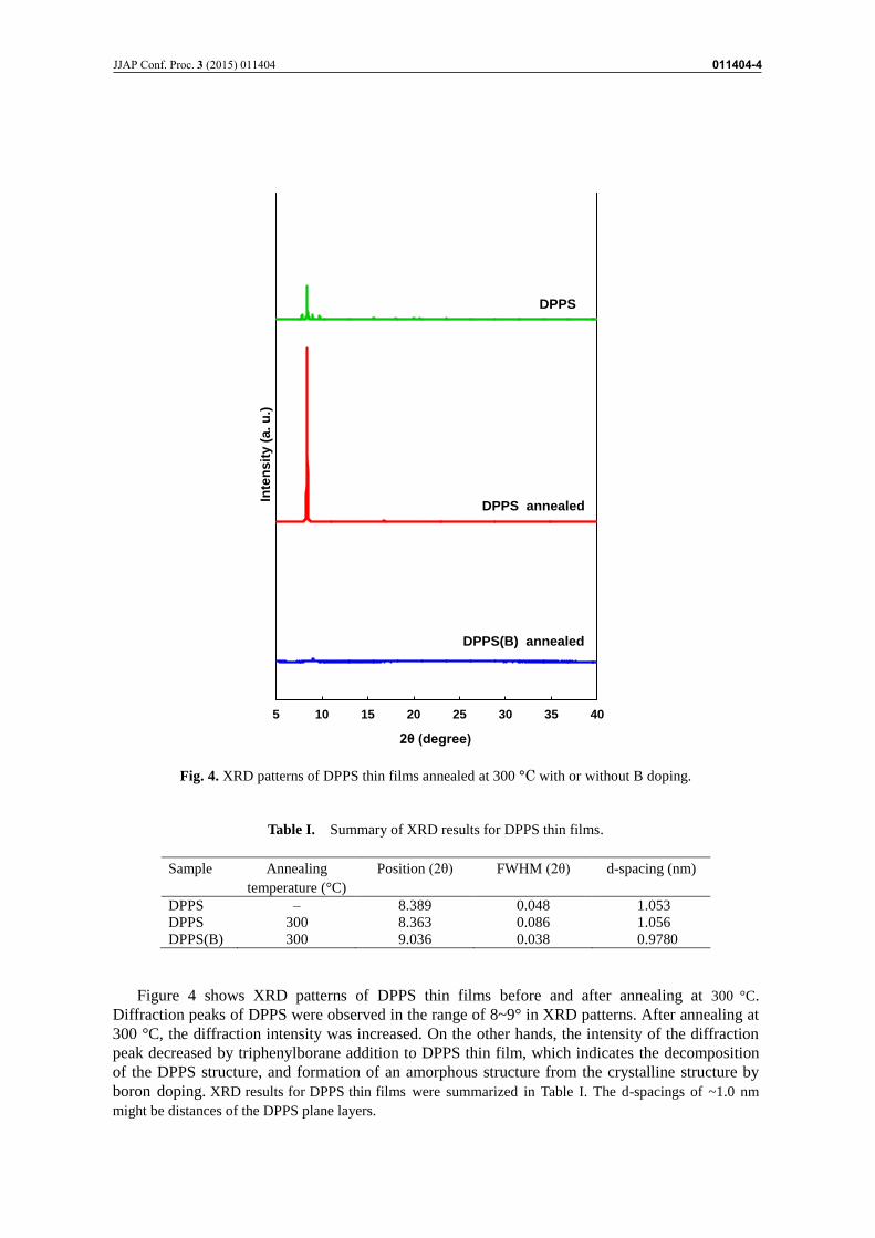
Fig. 4. XRD patterns of DPPS thin films annealed at 300 °C with or without B doping.
Table I. Summary of XRD results for DPPS thin films.
Sample Annealing
temperature (°C)
Position (2θ) FWHM (2θ) d-spacing (nm)
DPPS – 8.389 0.048 1.053
DPPS 300 8.363 0.086 1.056
DPPS(B) 300 9.036 0.038 0.9780
Figure 4 shows XRD patterns of DPPS thin films before and after annealing at 300 °C.
Diffraction peaks of DPPS were observed in the range of 8~9° in XRD patterns. After annealing at
300 °C, the diffraction intensity was increased. On the other hands, the intensity of the diffraction
peak decreased by triphenylborane addition to DPPS thin film, which indicates the decomposition
of the DPPS structure, and formation of an amorphous structure from the crystalline structure by
boron doping. XRD results for DPPS thin films were summarized in Table I. The d-spacings of ~1.0 nm
might be distances of the DPPS plane layers.
5 10 15 20 25 30 35 40
Inte
ns
ity (
a. u
.)
2θ (degree)
DPPS
DPPS(B) annealed
DPPS annealed
011404-4JJAP Conf. Proc. (2015) 0114043
J-V characteristics of the DPPS thin films were measured in the dark, and electrical resistances
of the DPPS thin films were calculated. Film thickness was measured to be ~200 nm by an atomic
force microscope. Volume resistivities of as-prepared, annealed, and annealed with B doping DPPS
were measured to be 6.6×10⁴, 5.6×10⁴, and 5.5×10⁴ Ω cm, respectively. The DPPS(B) thin films
exhibited decreased electrical resistances upon B doping and annealing.
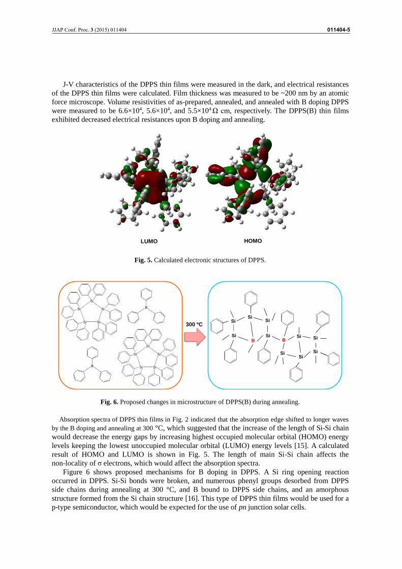
Fig. 5. Calculated electronic structures of DPPS.
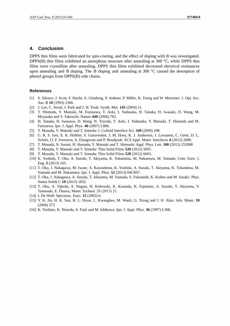
Fig. 6. Proposed changes in microstructure of DPPS(B) during annealing.
Absorption spectra of DPPS thin films in Fig. 2 indicated that the absorption edge shifted to longer waves
by the B doping and annealing at 300 °C, which suggested that the increase of the length of Si-Si chain
would decrease the energy gaps by increasing highest occupied molecular orbital (HOMO) energy
levels keeping the lowest unoccupied molecular orbital (LUMO) energy levels [15]. A calculated
result of HOMO and LUMO is shown in Fig. 5. The length of main Si-Si chain affects the
non-locality of σ electrons, which would affect the absorption spectra.
Figure 6 shows proposed mechanisms for B doping in DPPS. A Si ring opening reaction
occurred in DPPS. Si-Si bonds were broken, and numerous phenyl groups desorbed from DPPS
side chains during annealing at 300 °C, and B bound to DPPS side chains, and an amorphous
structure formed from the Si chain structure [16]. This type of DPPS thin films would be used for a
p-type semiconductor, which would be expected for the use of pn junction solar cells.
HOMOLUMO
Si Si
Si
Si
Si B
Si Si
Si
Si
Si
Si SiSi
SiSiB B
Si
Si
Si
Si
Si
300 ºC
B
011404-5JJAP Conf. Proc. (2015) 0114043
4. Conclusion
DPPS thin films were fabricated by spin-coating, and the effect of doping with B was investigated.
DPPS(B) thin films exhibited an amorphous structure after annealing at 300 °C, while DPPS thin
films were crystalline after annealing. DPPS thin films exhibited decreased electrical resistances
upon annealing and B doping. The B doping and annealing at 300 °C caused the desorption of
phenyl groups from DPPS(B) side chains.
References
[1] S. Silence, J. Scott, F. Hache, E. Ginsbrug, P. Jenkner, P. Miller, R. Twieg and W. Moermer: J. Opt. Soc.
Am. B 10 (1993) 2306.
[2] J. Lee, C. Seoul, J. Park and J. H. Youk: Synth. Met. 145 (2004) 11.
[3] T. Shimoda, Y. Matsuki, M. Furusawa, T. Aoki, I. Yudasaka, H. Tanaka, H. Iwasaki, D. Wang, M.
Miyasaka and Y. Takeuchi: Nature 440 (2006) 783.
[4] H. Tanaka, H. Iwasawa, D. Wang, N. Toyoda, T. Aoki, I. Yudasaka, Y. Matsuki, T. Shimoda and M.
Furusawa: Jpn. J. Appl. Phys. 46 (2007) L886.
[5] T. Masuda, Y. Matsuki and T. Simoda: J. Colloid Interface Sci. 340 (2009) 298.
[6] G. R. S. Iyer, E. K. Hobbie, S. Guruvenket, J. M. Hoey, K. J. Anderson, J. Lovaasen, C. Gette, D. L.
Schulz, O. F. Swenson, A. Elangovan and P. Boudjouk: ACS Appl. Mater. Interfaces 4 (2012) 2680.
[7] T. Masuda, N. Sotani, H. Hamada, Y. Matsuki and T. Shimoda: Appl. Phys. Lett. 100 (2012) 253908
[8] T. Masuda, Y. Matsuki and T. Simoda: Thin Solid Films 520 (2012) 5091.
[9] T. Masuda, Y. Matsuki and T. Simoda: Thin Solid Films 520 (2012) 6603.
[10] K. Yoshida, T. Oku, A. Suzuki, T. Akiyama, K. Tokumitsu, M. Nakamura, M. Yamada: Cent. Euro. J.
Eng. 3 (2013) 165.
[11] T. Oku, J. Nakagawa, M. Iwase, A. Kawashima, K. Yoshida, A. Suzuki, T. Akiyama, K. Tokumitsu, M.
Yamada and M. Nakamura: Jpn. J. Appl. Phys. 52 (2013) 04CR07.
[12] T. Oku, J. Nakagawa, A. Suzuki, T. Akiyama, M. Yamada, S. Fukunishi, K. Kohno and M. Sasaki: Phys.
Status Solidi C 10 (2013) 1832.
[13] T. Oku, A. Takeda, A. Nagata, H. Kidowaki, K. Kumada, K. Fujimoto, A. Suzuki, T. Akiyama, Y.
Yamasaki, E. Ōsawa, Mater. Technol. 28 (2013) 21.
[14] I. De Wolf: Spectrosc. Euro. 15 (2003) 6.
[15] Y. K. Jin, H. K. Sun, H. L. Hyun, L. Kwanghee, M. Wanli, G. Xiong and J. H. Alan: Adv. Mater. 18
(2006) 572
[16] K. Yoshino, K. Hosoda, A. Fujii and M. Ishikawa: Jpn. J. Appl. Phys. 36 (1997) L368.
011404-6JJAP Conf. Proc. (2015) 0114043


![increasing [HNP-2] · addition of HNP-2, which would show the effects of any fusion, aggregation, micellization or increase in size due to the presence of the peptide. Liposome dispersions](https://img.pdfslide.tips/doc/110x75/5fcf4304fc3ccc0e7807db8d/increasing-hnp-2-addition-of-hnp-2-which-would-show-the-effects-of-any-fusion.jpg)


![RESEARCH Open Access Effects of human papillomavirus …teosome pathway [5]. In addition, HPV E6 is able to bind several other cellular proteins, some of which can mediate transforming](https://img.pdfslide.tips/doc/110x75/608c28c235c25c778a5ca530/research-open-access-effects-of-human-papillomavirus-teosome-pathway-5-in-addition.jpg)


