Embed Size (px)
Citation preview

Enhancement- and depletion-modeAlGaN/GaN HEMTs on3C-SiC(111)/Si(111) pseudosubstrates
Wael Jatal1, Uwe Baumann2, Heiko O. Jacobs1, Frank Schwierz3, and J€org Pezoldt*,1
1 FG Nanotechnologie, Institut f€ur Mikro- und Nanotechnologien MacroNano1
und Institut f€ur Mikro- und Nanoelektronik, TU Ilmenau,Postfach 100565, 98684 Ilmenau, Germany
2 IMMS gGmbH, Ehrenbergstr. 27, 98693 Ilmenau, Germany3 FG Festk€orperelektronik, Institut f€ur Mikro- und Nanotechnologien MacroNano
1
und Institut f€ur Mikro- und Nanoelektronik, TUIlmenau, Postfach 100565, 98684 Ilmenau, Germany
Received 15 June 2016, revised 2 February 2017, accepted 2 February 2017Published online 28 February 2017
Keywords 3C-SiC, AlGaN, chemical vapor deposition, high electron mobility transistors, silicon, substrates
* Corresponding author: e-mail [email protected], Phone: þ49 3677 693412, Fax: þ49 3677 693709
The realization of depletion-mode planar and both enhance-ment- and depletion-mode tri-gate high electron mobilitytransistors (HEMTs) based on Al0.2Ga0.8N/AlN/GaN hetero-structures grown on silicon substrates using an ultrathin 3C-SiC transition layer is presented. This substrate configurationsimplifies heterostructure growth compared to SiC and thick3C-SiC substrates. The threshold voltage of the tri-gate devicesstrongly depends on the AlGaN/GaN body (fin) width. Atransition from depletion-mode to enhancement-mode opera-tion occurred at 110 nm body width for tri-gate devices withoutSi3N4 passivation, and is expected to occur at 75 nm for
devices with Si3N4 passivation. Threshold voltages of �0.25/0.35V were achieved at fin widths of 82/100 nm with/withoutSi3N4 passivation, respectively, for the tri-gate HEMTs incomparison to �3.5V for the planar HEMTs. Cutofffrequencies fT of 45GHz and maximum frequencies ofoscillation fmax of 50GHz have been measured for our best100-nm tri-gate enhancement-mode HEMTs, while depletion-mode planar HEMTs with the same gate length showed110GHz for both fT and fmax. This demonstrates theapplicability of the developed substrate configuration forhigh-performance device applications.
� 2017 WILEY-VCH Verlag GmbH & Co. KGaA, Weinheim
1 Introduction AlGaN/GaN high electron mobilitytransistors (HEMTs) are promising devices for radiofrequency (RF) power amplification [1], and combine highoperation frequencies with high output powers. For largescale fabrication of these devices three substrates can beused: sapphire, silicon carbide and silicon. The substrateproviding the highest thermal conductivity, smallest lattice,and thermal mismatch is SiC. These material properties arepreconditions for reliable high power density devices [2, 3].Meanwhile available with large diameters, the remainingdrawback of the SiC substrates is their relatively high price.A reasonable alternative solution compared to sapphireis silicon (Si), providing larger diameters at lower costscombined with a better thermal conductivity thansapphire [4–6]. However, the main drawback of thissubstrate is the large lattice and thermal mismatch aswell as chemical interactions between Si and the group
III-nitrides. The thermal and lattice mismatch leads to hightensile strains during heteroepitaxial growth and the coolingdown period. These strains cause high dislocation densities,cracks, and wafer warpage affecting the device processingand reliability. High temperature chemical reaction betweengallium and silicon roughens the Si surface and affectsdetrimentally the nucleation and growth of GaN and Si. Thiseffect is denoted as melt-back etching. A second effect is theappearance of autodoping effects in the III-nitride hetero-structure originating from diffusion of the substrate atoms,here silicon, into the heteroepitaxial layer [7]. Both, melt-back etching and Si outdiffusion, lead to void formation inthe Si substrate. Additionally, the incorporation of metalatoms into the Si substrate may change the resistivity of thesubstrate in the near interface region [8]. A possiblesolution, but not the only one, for the aforementionedchallenges is the incorporation of an additional layer
Phys. Status Solidi A 214, No. 4, 1600415 (2017) / DOI 10.1002/pssa.201600415
applications and materials science
statu
s
soli
di
www.pss-a.comph
ysi
ca a
� 2017 WILEY-VCH Verlag GmbH & Co. KGaA, Weinheim

improving the lattice mismatch and serving as a diffusionbarrier. Such a material is SiC, firstly employed byTakeuchi [9] and Davis [10]. Later, micrometer thick 3C-SiC(111) layers were used for the same purpose [6, 10–13].Albeit, it was shown that for reliable heteroepitaxialgrowth [14] and device fabrication thick silicon carbidelayers are not necessary [15–17]. A further advantage of aSiC transition layer is its high thermal conductivity. A recentreview of the influence of the buffer layer on the AlGaN/GaN heterostructure and HEMT performance on Sisubstrates is given in [18].
Typically, AlGaN/GaN HEMTs are depletion-mode(D-mode) devices [19], but for simple circuit design andimproved system reliability, enhancement-mode (E-mode)are desired. A recent realization of E-mode HEMTs aremulti-mesa-channel (MMC) structures or nanochannelarrays (NCA). They employ a tri-gate structure [19, 20–26],where the gate is wrapped around narrow AlGaN/GaNbodies from three sides (from the top and from bothperpendicular sidewalls), similar to the tri-gate Si MOS-FETs which currently enjoy increasing popularity. Otherpossibilities to fabricate E-mode AlGaN/GaN HEMTs areultrathin AlGaN barriers [27], gate recess [28], or fluorineplasma treatment [29]. In this article, we report on theprocessing and characterization of D- and E-mode tri-gateHEMTs based on GaN/Al0.2Ga0.8N/AlN/GaN heterostruc-tures grown on Si substrates using an ultrathin SiC transitionlayer.
2 Experimental2.1 LPCVD growth of the SiC transition
layer The 3C-SiC/Si(111) pseudosubstrates for the subse-quent GaN growth were prepared using a two-step growthmethod developed by Nishino [28, 30]. First, a very thin SiClayer (3 nm) is realized by carbonization of the Si surfacewhere only a carbon-based precursor (C2H4) is present in thereactor. Next a silicon precursor (SiH4) is added, leading tothe epitaxial growth of a thicker SiC layer. We used a lowpressure CVD process at a substrate temperature of1060 8C [29, 31]. The background pressure in the UHVchamber was 5� 10�9mbar and the process pressure wasabout 0.0014mbar. The epitaxial growth was monitored insitu by spectroscopic ellipsometry and reflection of highenergy electron diffraction. The chosen silicon carbidethickness prevented the Ga-induced melt back etching andthe Si-outdiffusion in the subsequent metal organicchemical vapour deposition (MOCVD) growth [13–16].The needed 3C-SiC(111) layer thickness was 50 nm.
2.2 MOCVDgrowth The heteroepitaxial growth ofthe GaN/Al0.2Ga0.8N/AlN/GaN heterostructures using anactive layer stack of GaN/Al0.2Ga0.8N/AlN with layerthicknesses of 2/20/1 nm on the GaN buffer wasperformed by MOCVD. First, a 100-nm AlN nucleationlayer was grown at 950 8C. The formation of anamorphous and nonstoichiometric silicon nitride layerwas suppressed by shortly forerunning the aluminum
precursor trimethylaluminium (TMAL). After recrystal-lization at 1160 8C, 500 nm GaN growth was started at1060 8C and proceeded at 1150 8C. Strain engineeringwas done by inserting an AlN layer during GaNbuffer growth to prevent cracking of the GaN bufferlayer during cool-down. On top of the AlN insertionlayer a 500 nm buffer was grown, followed by thebarrier consisting of an 1-nm AlN layer and a 20-nmAl0.2Ga0.8N. The GaN cap was 2 nm thick. Thecharacteristics of the 2DEG were measured by capaci-tance–voltage and Hall measurements, which revealed anelectron density of 7.5� 1012 cm�2 and a low fieldmobility of 1760 cm2 Vs�1, respectively.
2.3 Processing HEMT devices Figure 1 showsscanning electron (SEM) and optical microscopy (OM)images of the gate region and the device layout of fabricatedplanar and tri-gate AlGaN/AlN/GaN devices. The channelof the tri-gate HEMTs consists of a set of parallelnanochannel bodies forming a nanochannel body array.
The lateral device dimensions were defined by electronbeam lithography. Device isolation was realized using amesa structure. The mesa and the body arrays of the tri-gatedevices were fabricated by dry etching in a chlorine-basedplasma process. Ohmic contacts were realized using astandard Ti/Al/Ti/Au metallization scheme. The thicknessesof the different metal layers were 20/80/30/100 nm. Contactannealing was performed in a rapid thermal processingreactor at 850 8C for 45 s. The contact resistance hasbeen determined by the transmission line method.Current–voltage characteristics measured in the voltage
Figure 1 SEM images of the channel region of an E-mode tri-gateHEMT showing the nanochannel bodies and the gate with a gatelength Lg of 0.1mm and a body width of 82 nm (a) and of a D-modeplanar AlGaN/GaN HEMT showing the gate with Lg of 0.1mm (c).OM images displaying the device layout of the tri-gate (b) andthe planar (d) HEMTs with the source (S), gate (G) and drain(D) including the contact pads.
1600415 (2 of 7) W. Jatal et al.: Enhancement- and depletion-mode AlGaN/GaN HEMTs
� 2017 WILEY-VCH Verlag GmbH & Co. KGaA, Weinheim www.pss-a.com
ph
ysic
a ssp stat
us
solid
i a

range�1 toþ1V using a HP4145 semiconductor parameteranalyzer were used to extract the contact resistance. Thespecific contact resistance and the contact resistance ofthe Ti/Al/Ti/Au contacts were 1.12� 10�7V cm2 and0.13� 0.01Vmm, respectively. A 3 nm thick SiN passiv-ation layer was deposited on both the planar and the tri-gateAlGaN/AlN/GaN HEMTs using plasma enhanced chemicalvapor deposition at 350 8C to reduce the surface effectsresponsible for limiting both the RF performance andbreakdown voltages of the devices [32]. Ni/Au gates werepatterned by electron beam lithography and lift-off, andwere located in the center between the source and the drain,with a drain-source separation of 2mm. The tri-gatetransistors have a rectangular gate, whereas the planartransistors possess a T-gate. Finally, the overlay metalliza-tion and contact pads were formed by depositing Ti/Au. On-wafer RF measurements in the 0.1–50GHz range werecarried out with a Casacade Microtech Probe and aHP8510B network analyzer.
3 Results and discussion The dependence of thethreshold voltage on the body width of the tri-gate HEMTswith and without SiN passivation is shown in Fig. 2.
The threshold voltage shows a nearly linear dependenceon the body width. At a body width of 110 nm without SiNpassivation, a threshold voltageVTH¼ 0Vwas achieved. Forthe identical heterostructure with SiN passivation, a zerothreshold voltage is expected for a bodywidth around 70 nm.For unpassivated tri-gate HEMTs, a maximum thresholdvoltage of 0.35V was obtained at a body width of 100 nm.Therefore, normally off operation can be achieved byproperly choosing the body width. The reasons for thedepletion of the 2DEG in tri-gate structures are threefold.First, the top-gate (the gate portion located on the body top)depletes the 2DEGas in planarHEMTstructures. Second, thegate portions covering the vertical body sidewalls cause afringing field (curved field lines from the sidewall gatestoward the 2DEG), which does not exist in planar HEMTs.The thirdeffect contributing to the2DEGdepletionoriginates
from strain reduction (partial relaxation) in the narrowAlGaN/GaN bodies [22]. The steeper threshold voltagedependence in comparison to Ref. [26] was achieved bychanging the etching conditions to improve the sidewallgeometry. The SiN passivation increases the effective barrierthickness and changes the stress state and interface statedensity. In the present case, these effects decrease the bodywidth needed for normal off, i.e., E-mode, operation. Thethreshold voltage shift in the tri-gate devices with SiNpassivation originates mainly from two effects, namely thepositive charge in the SiN layer [33] and the stress induced bythe deposited SiN [34] leading to an increase of the chargecarrier density of the 2DEG. The effect of the body widthonVTH fromFig. 2 is supported by simulations carried out fortri-gate AlGaN/GaN HEMTs in Ref. [35].
Figure 3(a) and (b) show the output characteristics of tri-gate AlGaN/GaNHEMTswithout and with SiN passivation,as well as of a planar HEMT (Fig. 3c). The transistor withSiN passivation has a body width, Wbody, of 100 nm, a gatelength Lg¼ 100 nm, and shows D-mode operation, whereasthe transistor without SiN passivation, Wbody¼ 82 nm, andLg¼ 200 nm is an E-mode device. Figure 3(c) displays theoutput characteristics of a planar HEMT fabricated on thesame heterostructure using a 100-nm T-gate. The on-offratios Ion/Ioff of the devices are 10
4 for the E-mode tri-gatedevice without SiN, 105 for the D-mode tri-gate device withSiN, and 108 for the planar device.
Figure 4 shows the transfer characteristics of the devicesfrom Fig. 3. The drain current and the transconductanceare normalized to the effective channel width. The tri-gateHEMTs demonstrate reasonably good current–voltagebehavior. Maximum drain current densities of 445 and655mAmm�1 were achieved for tri-gate HEMTs withoutand with SiN passivation, respectively, obtained for a gate-source voltage VGS of 4V and a drain-source voltage VDS of10V. The transconductances gm reached values of 120 and200mSmm�1 at VDS¼ 5V for the tri-gate HEMTs withoutand with SiN passivation. The increased drain currents andtransconductances of the passivated devices stem frompositive charges in the SiN causing an increase of the chargecarrier density in the 2DEG. For the planar AlGaN/GaNHEMT, a drain current density of 600mAmm�1 and atransconductance of 180mSmm�1 have been obtained forVGS¼ 0V and VDS¼ 10V. The output characteristics of theE- and D-mode HEMTs exhibit a reasonably goodsaturation, which is essential for good RF performance.The transconductance gm for the E-mode devices reachedvalues of 190mSmm�1 at VDS¼ 5V. A threshold voltage of�0.25V was achieved for the tri-gate device with SiNpassivation, which represents a significant shift toward E-mode operation in comparison to the threshold voltage of�3.5V for the planar D-mode HEMT. A positive thresholdvoltage of 0.35� 0.08V was obtained extrapolating thetransfer characteristic shown in Fig. 3(a) for the devicewithout SiN passivation.
Figure 5 displays the gate leakage characteristics ofthe HEMTs measured at VDS¼ 0V. The gate leakage of the
Figure 2 Threshold voltage VTH versus body width Wbody of thetri-gate HEMTs with and without SiN passivation.
Phys. Status Solidi A 214, No. 4 (2017) (3 of 7) 1600415
www.pss-a.com � 2017 WILEY-VCH Verlag GmbH & Co. KGaA, Weinheim
Original
Paper
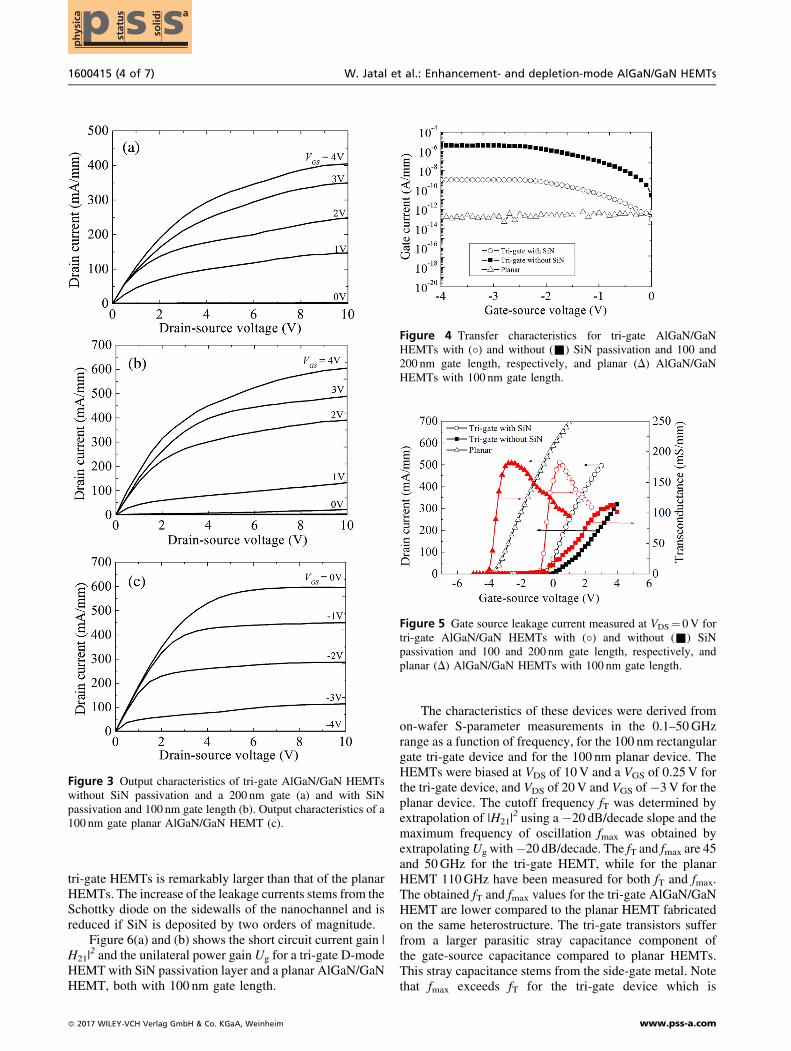
tri-gate HEMTs is remarkably larger than that of the planarHEMTs. The increase of the leakage currents stems from theSchottky diode on the sidewalls of the nanochannel and isreduced if SiN is deposited by two orders of magnitude.
Figure 6(a) and (b) shows the short circuit current gain |H21|
2 and the unilateral power gain Ug for a tri-gate D-modeHEMT with SiN passivation layer and a planar AlGaN/GaNHEMT, both with 100 nm gate length.
The characteristics of these devices were derived fromon-wafer S-parameter measurements in the 0.1–50GHzrange as a function of frequency, for the 100 nm rectangulargate tri-gate device and for the 100 nm planar device. TheHEMTs were biased at VDS of 10V and a VGS of 0.25V forthe tri-gate device, and VDS of 20V and VGS of�3V for theplanar device. The cutoff frequency fT was determined byextrapolation of |H21|
2 using a�20 dB/decade slope and themaximum frequency of oscillation fmax was obtained byextrapolatingUg with�20 dB/decade. The fT and fmax are 45and 50GHz for the tri-gate HEMT, while for the planarHEMT 110GHz have been measured for both fT and fmax.The obtained fT and fmax values for the tri-gate AlGaN/GaNHEMT are lower compared to the planar HEMT fabricatedon the same heterostructure. The tri-gate transistors sufferfrom a larger parasitic stray capacitance component ofthe gate-source capacitance compared to planar HEMTs.This stray capacitance stems from the side-gate metal. Notethat fmax exceeds fT for the tri-gate device which is
Figure 4 Transfer characteristics for tri-gate AlGaN/GaNHEMTs with (�) and without (&) SiN passivation and 100 and200 nm gate length, respectively, and planar (D) AlGaN/GaNHEMTs with 100 nm gate length.
Figure 5 Gate source leakage current measured at VDS¼ 0V fortri-gate AlGaN/GaN HEMTs with (�) and without (&) SiNpassivation and 100 and 200 nm gate length, respectively, andplanar (D) AlGaN/GaN HEMTs with 100 nm gate length.
Figure 3 Output characteristics of tri-gate AlGaN/GaN HEMTswithout SiN passivation and a 200 nm gate (a) and with SiNpassivation and 100 nm gate length (b). Output characteristics of a100 nm gate planar AlGaN/GaN HEMT (c).
1600415 (4 of 7) W. Jatal et al.: Enhancement- and depletion-mode AlGaN/GaN HEMTs
� 2017 WILEY-VCH Verlag GmbH & Co. KGaA, Weinheim www.pss-a.com
ph
ysic
a ssp stat
us
solid
i a

uncommon if rectangular gates are used, but was alsoobserved in Ref. [23, 26].
Figure 7 shows the cutoff frequency of the fabricatedE-mode tri-gate and D-mode planar AlGaN/GaN HEMTs asa function of gate length, together with the correspondingdata of AlGaN/GaN HEMTs on SiC and Si substrates
compiled from the literature. The cutoff frequencies of theE- and D-mode tri-gate HEMTs are still below those of theD-mode planar devices, but show a pronounced dependenceon the gate length between 100 and 250 nm. The degradedcutoff frequencies of the E-mode HEMTs are again causedby the larger stray capacitance of the tri-gate transistorconfiguration [36].
Figure 8 shows fT and fmax of our tri-gate HEMTs withand without SiN passivation as a function of body width. fTand fmax increase continuously for decreasing body width.Furthermore, fT and fmax of the tri-gate transistor with SiNpassivation are higher than those of the tri-gate transistorwithout SiN. The decreased fT and fmax of the tri-gate HEMTwithout SiN passivation compared to the tri-gate transistorwith SiN passivation stems from the increased gatecapacitance and the reduced charge carrier densities ofthe 2DEG.
4 Conclusions Tri-gate and planar HEMTs based ona GaN/Al0.2Ga0.8N/AlN/GaN heterostructure grown on Sisubstrates using a SiC transition layer have been fabricatedand characterized. The critical body width for the transitionfrom D- to E-mode operation was 110 nm for our tri-gatedevices without SiN passivation and 75 nm for the tri-gateHEMTs with passivation. Cutoff frequencies of 45 and110GHz have been obtained for our best tri-gate and planar100-nm gate HEMTs, respectively, and the maximumfrequencies of oscillation of these devices are 50GHz (tri-gate) and 110GHz (planar).
References
[1] U. K. Mishra, L. Shen, T. E. Kazior, and Y.-F. Wu, Proc.IEEE 96, 287 (2008).
[2] Y.-F.Wu, D. Kapolnek, J. P. Ibbetson, P. Parikh, B. P. Keller,and U. K. Mishra, IEEE Trans. Electron Devices 48, 586(2001).
[3] Y. Cordier, M. Hugues, F. Semond, F. Natali, P. Lorenzini, Z.Bougrioua, J. Massies, E. Frayssinet, B. Beaumont, P. Gibart,and J.-P. Faurie, J. Cryst. Growth 278, 383 (2005).
Figure 6 (a) Short-circuit current gain and unilateral power gainversus frequency for a tri-gate AlGaN/GaN HEMT (a), and for aplanar device (b), both with 100-nm gates.
Figure 7 Comparison of the cutoff frequencies of our E-modetri-gate and D-mode planar GaN/Al0.2Ga0.8N/AlN/GaN HEMTson Si with our last results [17, 26, 37, 38] and with the best fT datareported by other groups for AlGaN/GaN HEMTs on Si [39–46]and on SiC [4, 47–53].
Figure 8 Comparison of the fT and fmax versus body width of thenanochannels of the tri-gate GaN/Al0.2Ga0.8N/AlN/ GaN HEMTwithout and with SiN passivation layer with Ti/Al/Ti/Au ohmiccontacts. 100 and 200 denote the gate length in nm.
Phys. Status Solidi A 214, No. 4 (2017) (5 of 7) 1600415
www.pss-a.com � 2017 WILEY-VCH Verlag GmbH & Co. KGaA, Weinheim
Original
Paper

[4] D. C. Dumka, C. Lee, H. Q. Tsern, P. Saumier, and M.Kumar, Electron. Lett. 40, 1023 (2004).
[5] J. W. Johnson, E. L. Piner, A. Vescan, R. Therrien, P.Rajagopal, J. C. Roberts, J. D. Brown, S. Singhal, andK. L. Linthicum, IEEE Electron Device Lett. 25, 459(2004).
[6] Y. Cordier, M. Portail, S. Chenot, O. Tottereau, M. Zielinski,and Th. Chassagne, J. Cryst. Growth 310, 4417 (2008).
[7] A. Dadger, A. Strittmatter, J. Blasing, M. Poschenrieder, O.Contreras, P. Veit, T. Riemann, F. Bertram, A. Reiher, A.Krtschil, A. Diez, T. Hempel, T. Finger, A. Kasic, M.Schubert, D. Bimberg, F. A. Ponce, J. Christen, and A. Krost,Phys. Status Solidi C 0, 1583 (2003).
[8] H. Witte, C. Hums, C. Baer, K.-M. Guenther, A. Krtschil, A.Dadgar,andA.Krost, J.Phys.D:Appl.Phys.42, 205103(2009).
[9] T. Takeuchi, H. Amano, K. Hiramatsu, N. Sawaki, and I.Akasaki, J. Cryst. Growth 115, 634 (1991).
[10] R. F. Davis, Th Gehrke, K. J. Linthicum, E. Preble, P.Rajagopal, G Ronning, Ch Zorman, and M Mehregany, J.Cryst. Growth 231, 335 (2001).
[11] Y. Cordier, S. Chenot, M. La€ugt, O. Tottereau, S. Joblot, F.Semond, J. Massies, L. D. Cioccio, and H. Moriceau, Phys.Status Solidi C 4, 2670 (2007).
[12] Y. Cordier, M. Portail, S. Chenot, O. Tottereau, M. Zielinski,and T. Chassagne, Phys. Status Solidi C 5, 1983 (2008).
[13] Y. Cordier, M. Portail, S. Chenot, O. Tottereau, M.Zielinski, and T. Chassagne, Mater. Sci. Forum 600–603,1277 (2009).
[14] Y. Cordier, E. Frayssinet, M. Portail, M. Zielinski, T.Chassagne, M. Korytov, A. Courville, S. Roy, M. Nemoz, M.Chmielowska, P. Venn�egu�es, H. P. D. Schenk, M. Kennard,A. Bavard, and D. Rondi, J. Cryst. Growth 398, 23 (2014).
[15] K. Tonisch, W. Jatal, R. Granzner, M. Kittler, U. Baumann,F. Schwierz, and J. Pezoldt, Mater. Sci. Forum 645–648,1219–1222 (2010).
[16] K. Tonisch, W. Jatal, F. Niebelschuetz, H. Romanus, F.Schwierz, U. Baumann, and J. Pezoldt, Thin Solid Films 520,491 (2011).
[17] W. Jatal, K. Tonisch, U. Baumann, F. Schwierz, and J.Pezoldt, Mater. Sci. Forum 740–742, 1115 (2013).
[18] Y. Cordier, Phys. Status Solidi A 212, 1049 (2015).[19] O. Ambacher, B. Foutz, J. Smart, J. Shealy, N. Weimann, K.
Chu, M. Murphy, A. Sierakowski, W. Schaff, L. F. Eastman,R. Dimitrov, A. Mitchell, and M. Stutzmann, J. Appl. Phys.87, 334 (2000).
[20] K. Ohi and T. Hashizume, Jpn. J. Appl. Phys. 48, 081002(2009).
[21] K. Ohi, J. T. Asubar, K. Nishiguchi, and T. Hashizume, IEEETrans. Electron Devices 60, 2997 (2013).
[22] S. H. Liu, Y. Cai, R. M. Gong, J. Y. Wang, C. H. Zeng, W. H.Shi, Z. H. Feng, J. J. Wang, J. Y. Yin, P. W. Cheng, H. Qin,and B. S. Zhang, Chin. Phys. Lett. 28, 077202 (2011).
[23] S. Liu, Y. Cai, G. Gu, J. Wang, C. Zeng, W. Shi, Z. Feng, H.Qin, Z. Cheng, K. J. Chen, and B. Zhang, IEEE ElectronDevice Lett. 33, 354 (2012).
[24] B. Lu, E. Matioli, and T. Palacios, in: Proc. 24th Intern.Symp. on Power Semiconductor Devices and ICs, Bruges,Belgium, 2012 (IEEE, Piscataway, 2012), pp. 33–36.
[25] B. Lu, E. Matioli, and T. Palacios, IEEE Electron DeviceLett. 33, 360 (2012).
[26] W. Jatal, U. Baumann, H. O. Jacobs, F. Schwierz, and J.Pezoldt, Mater. Sci. Forum 858, 1174 (2016).
[27] K. Shinohara, D. C. Regan, Y. Tang, A. I. Corrion, D. F.Brown, J. C. Wong, J. F. Robinson, H. H. Fung, A. Schmitz,T. C. Oh, S. J. Kim, P. S. Chen, R. G. Nagele, A. D. Mar-gomenos, and M. Micovic, IEEE Trans. Electron Devices 60,2982 (2013).
[28] A. Wakeijima, A. Ando, A. Watanabe, K. Inoue, T. Kubo,Y. Osada, R. Kamimura, and T. Egawa, Appl. Phys. Express8, 026502 (2015).
[29] Y. Cai, Y. Zhou, K. J. Chen, and K. M. Lau, IEEE ElectronDev. Lett. 26, 435 (2005).
[30] S. Nishino, J. A. Powell, and H. A. Will, Appl. Phys. Lett. 42,460 (1983).
[31] Ch. F€orster, V. Cimalla, O. Ambacher, and J. Pezoldt, Mater.Sci. Forum 483–485, 201 (2005).
[32] B. M. Green, K. K. Chu, E. M. Chumbes, J. A. Smart, J. A.Shealy, and L. F. Eastman, IEEE Electron Device Lett. 21,268 (2000).
[33] Z. Liu, S. Huang, Q. Bao, X. Wang, K. Wei, H. Jiang, H.Cui, J. Li, C. Zhao, X. Liu, J. Zhang, Q. Zhou, W. Chen, B.Zhang, and L. Jia, J. Vac. Sci. Technol. B 34, 041202(2016).
[34] M. Azize and T. Palacios, Appl. Phys. Lett. 98, 042103(2011).
[35] M. Alsharef, R. Granzner, and F. Schwierz, IEEE Trans.Electron Devices 60, 3335–3341 (2013).
[36] D. S. Lee, H. W. Wang, A. Hsu, M. Azize, O. Laboutin,Y. Cao, J. W. Johnson, E. Beam, A. Ketterson, M. L.Schuette, P. Saunier, and T. Palacios, IEEE Electron DeviceLett. 34, 969 (2013).
[37] W. Jatal, U. Baumann, K. Tonisch, F. Schwierz, and J.Pezoldt, IEEE Electron Device Lett. 36, 123 (2015).
[38] W. Jatal, K. Tonisch, U. Baumann, F. Schwierz, and J.Pezoldt, in: Conf. Proc. 10th Inter. Conf. on AdvancedSemiconductor Devices and Microsystems, SmoleniceCastle, Slovakia, (IEEE, Piscataway, 2014), pp. 117–120.
[39] F. Medjdoub, N. Waldhoff, M. Zegaoui, B. Grimbert, N.Rolland, and P. A. Rolland, IEEE Electron Device Lett. 32,1230 (2011).
[40] D.Marti, S. Tirelli, A. R. Alt, J. Roberts, and C. R. Bolognesi,IEEE Electron Device Lett. 33, 1372 (2012).
[41] F. Medjdoub, M. Zegaoui, and N. Rolland, Electron. Lett. 47,1345 (2011).
[42] F. Medjdoub, M. Zegaoui, D. Ducatteau, N. Rolland, andP. A. Rolland, IEEE Electron Device Lett. 32, 874 (2011).
[43] D. Ducatteau, A. Minko, V. Hoël, E. Morvan, E. Delos, B.Grimbert, H. Lahreche, P. Bove, C. Gaqui�ere, J. C. DeJaeger, and S. Delage, IEEE Electron Device Lett. 27, 7(2006).
[44] Z. H. Liu, G. I. Ng, S. Arulkumaran, Y. K. Thu Maung, K. L.Teo, S. C. Foo, V. Sahmuganathan, T. Xu, and C. H. Lee,IEEE Electron Device Lett. 31, 96 (2010).
[45] S. Rennesson, F. Lecourt, N. Defrance, M. Chmielowska, S.Chenot, M. Lesecq, V. Hoel, E. Okada, Y. Cordier, and J.-C. De Jaeger, IEEE Trans. Electron Devices 60, 3105(2013).
[46] P. D. Christy, Y. Katayama, A. Wakejima, and T. Egawa,Electron. Lett. 51, 1366 (2015).
[47] K. Shinohara, D. Regan, A. Corrion, D. Brown, Y. Tang, J.Wong, G. Candia, A. Schmitz, H. Fung, S. Kim, and M.Micovic, in: 2012 Intern. Electron Device Meeting, Techni-cal Digest, San Fransisco, CA, USA, 2012 (IEEE, Piscat-away, 2012), pp. 27.2.1–27.2.4.
1600415 (6 of 7) W. Jatal et al.: Enhancement- and depletion-mode AlGaN/GaN HEMTs
� 2017 WILEY-VCH Verlag GmbH & Co. KGaA, Weinheim www.pss-a.com
ph
ysic
a ssp stat
us
solid
i a

[48] K. Shinohara, D. Regan, I. Milosavljevic, A. L. Corrion, D. F.Brown, P. J. Willadsen, C. Butler, A. Schmitz, S. Kim, V.Lee, A. Ohoka, P. M. Asbeck, and M. Micovic, IEEEElectron Device Lett. 32, 1074 (2011).
[49] T. Palacios, A. Chakraborty, S. Heikman, S. Keller, S. P.DenBaars, and U. K. Mishra, IEEE Electron Device Lett. 27,13 (2006).
[50] U. Singisetti, M. Hoi Wong, J. S. Speck, and U. K. Mishra,IEEE Electron Device Lett. 33, 26 (2012).
[51] V. Kumar, W. Lu, R. Schwindt, A. Kuliev, G. Simin, J. Yang,M. Asif Khan, and I. Adesida, IEEE Electron Device Lett. 23,455 (2002).
[52] V. Kumar, D. H. Kim, A. Basu, and I. Adesida, IEEEElectron Device Lett. 29, 18 (2008).
[53] D.-H. Youn, V. Kumar, J.-H. Lee, R. Schwindt, W.-J.Chang, J.-Y. Hong, C.-M. Jeon, S.-B. Bae, M.-R. Park,K.-S. Lee, J.-L. Lee, and I. Adesida, Electron. Lett. 39, 566(2003).
Phys. Status Solidi A 214, No. 4 (2017) (7 of 7) 1600415
www.pss-a.com � 2017 WILEY-VCH Verlag GmbH & Co. KGaA, Weinheim
Original
Paper