Embed Size (px)
Citation preview
Fundamentals of Semiconductor Physics
万 歆Zhejiang Institute of Modern Physics
[email protected]://zimp.zju.edu.cn/~xinwan/
Fall 2007

Preview• The electrical properties of a singlecrystal materials are determined by the
chemical composition and the arrangement of atoms in the solid. This can be understood in the quantum theory of solids.
• In a real crystal, the lattice is not perfect, containing imperfections or defects. The presence of substitutional impurity atoms can dramatically alter the electrical properties of a semiconductor material; in fact, we intentionally add impurities (by doping) to it to change its conductivity.
• The number of electrons in a semiconductor is very large, which should be treated by statistical mechanics. One is interested in the statistical behavior of the system.
• The process by which electrons move is called transport. Nearequilibrium and nonequilibrium processes are needed to understand the currentvoltage characteristics of semiconductor devices.
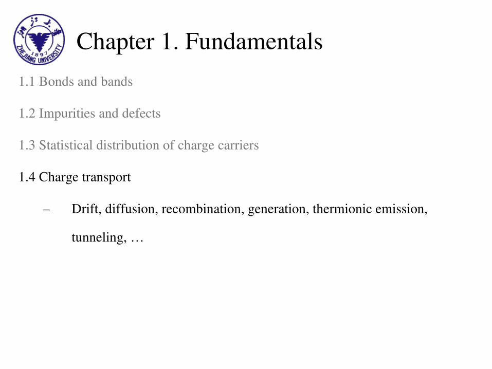
Chapter 1. Fundamentals1.1 Bonds and bands
1.2 Impurities and defects
1.3 Statistical distribution of charge carriers
1.4 Charge transport
Total 6 hours.
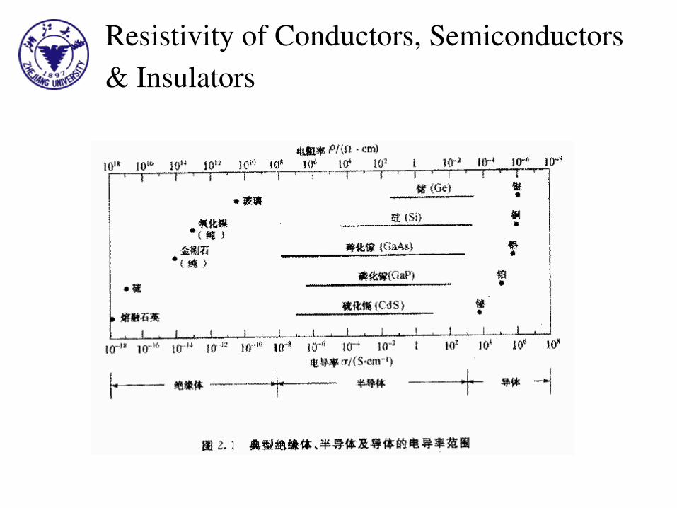
Resistivity of Conductors, Semiconductors & Insulators

Semiconductorforming Elements
TeSbSnInCd
SeAsGeGaZn
SPSiAl
ONCB
Yu/Cardona
Chapter 1. Fundamentals
1.1 Bonds and bands– Crystal structures– Bond picture– Band picture
• “Nearly free” electron model• Tightbinding model (LCMO)• k∙p perturbation
1.2 Impurities and defects
1.3 Statistical distribution of charge carriers
1.4 Charge transport
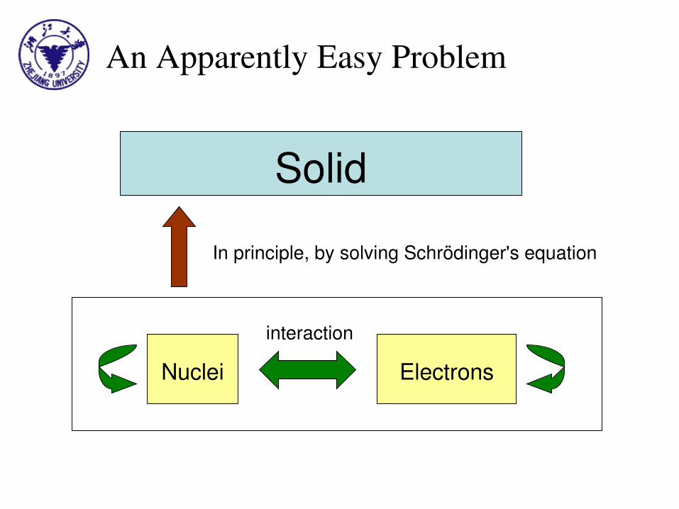
An Apparently Easy Problem
Solid
Nuclei Electronsinteraction
In principle, by solving Schrödinger's equation
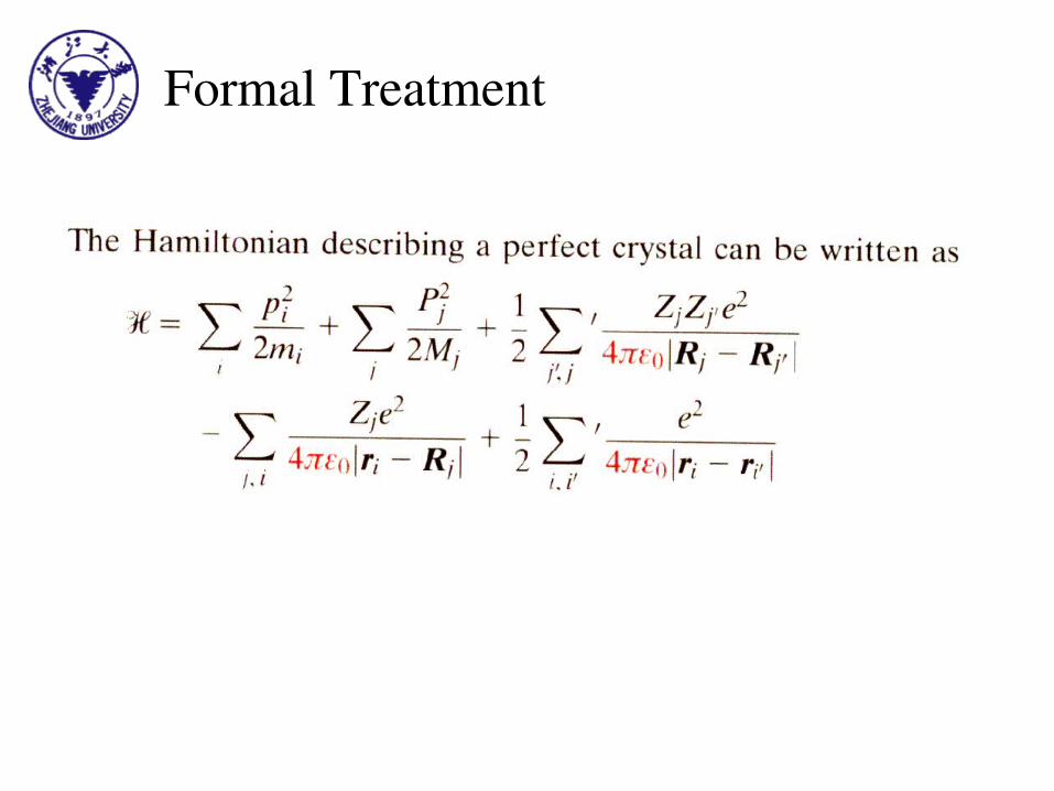
Formal Treatment

Approximation 1Separation of electrons into
valence electrons and core electrons
Ion cores = core electrons + nuclei
e.g. Si: [Ne] 3s23p2
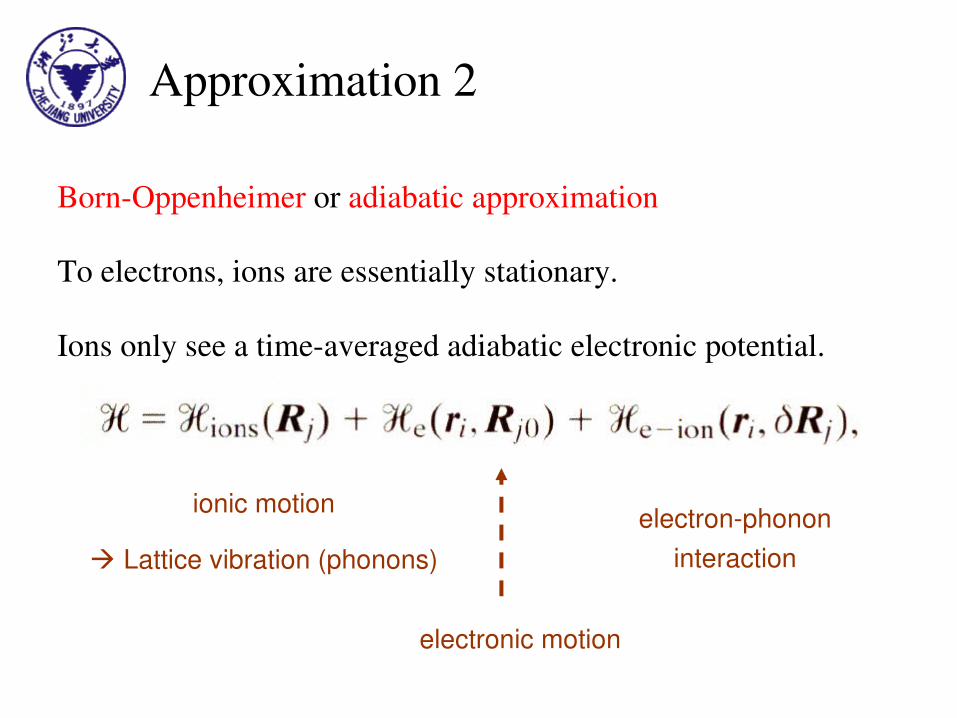
Approximation 2
BornOppenheimer or adiabatic approximation
To electrons, ions are essentially stationary.
Ions only see a timeaveraged adiabatic electronic potential.
electronphonon interaction
ionic motion
Lattice vibration (phonons)
electronic motion
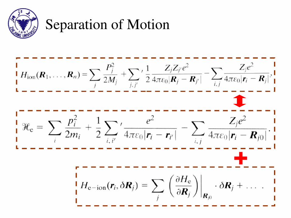
Separation of Motion
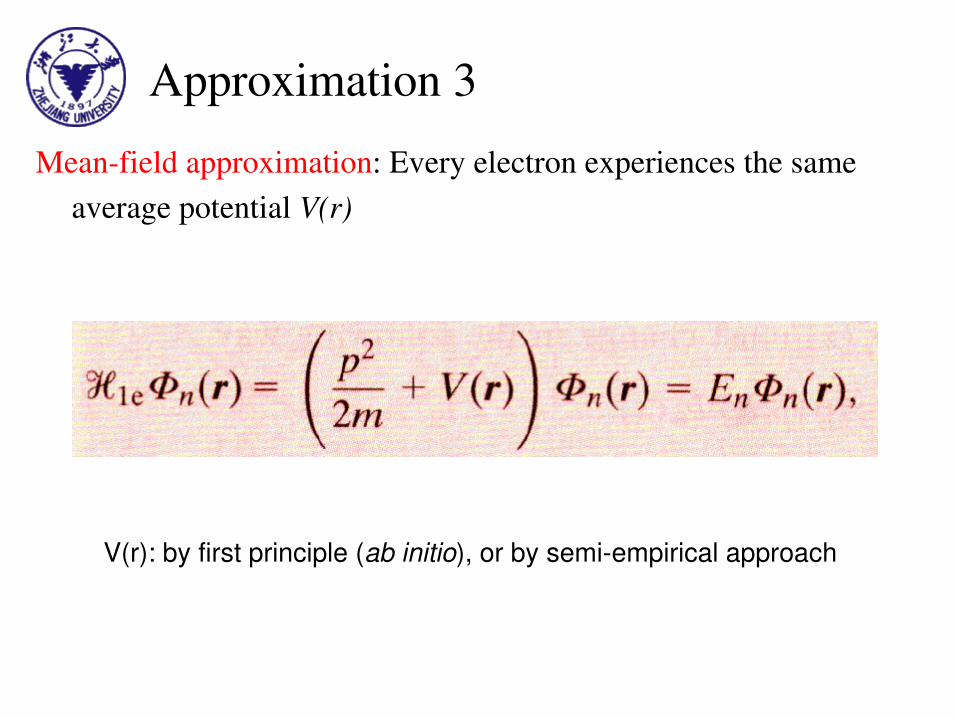
Approximation 3Meanfield approximation: Every electron experiences the same
average potential V(r)
V(r): by first principle (ab initio), or by semiempirical approach
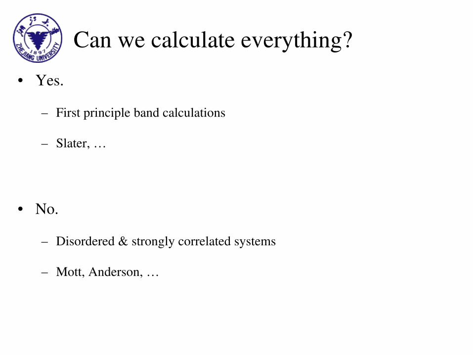
Can we calculate everything?• Yes.
– First principle band calculations
– Slater, …
• No.
– Disordered & strongly correlated systems
– Mott, Anderson, …
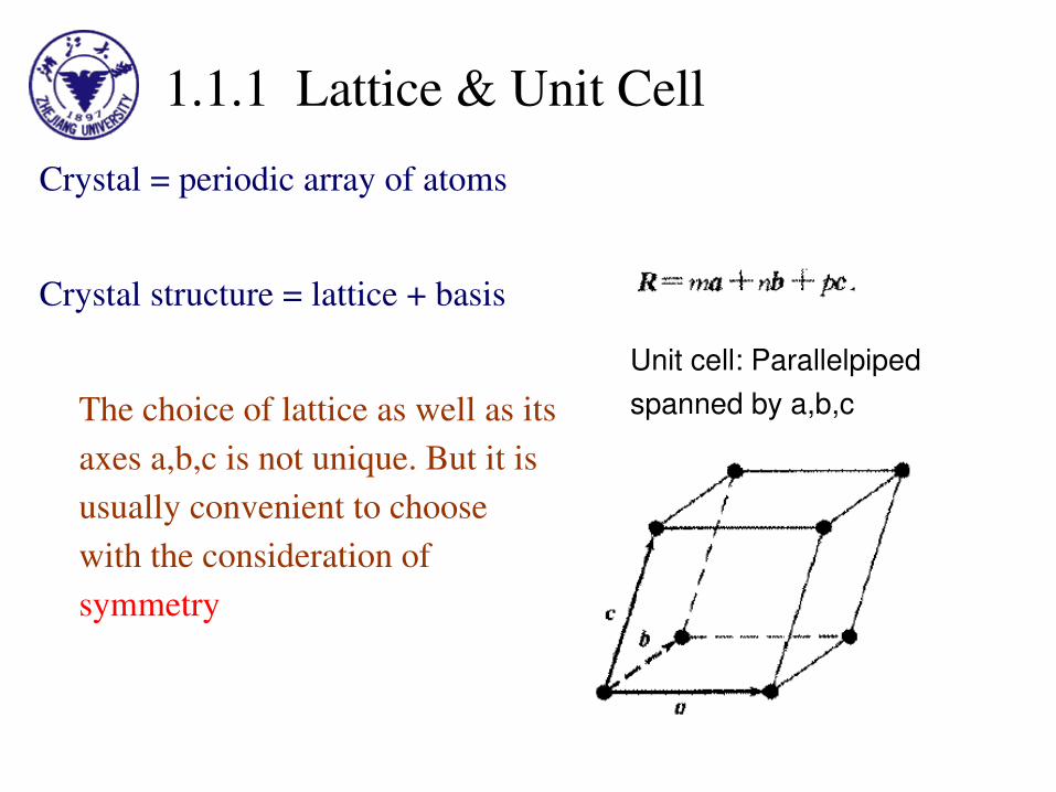
1.1.1 Lattice & Unit CellCrystal = periodic array of atoms
Crystal structure = lattice + basis
The choice of lattice as well as its axes a,b,c is not unique. But it is usually convenient to choose with the consideration of symmetry
Unit cell: Parallelpiped spanned by a,b,c
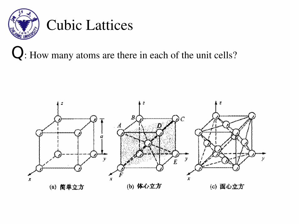
Cubic Lattices
Q: How many atoms are there in each of the unit cells?
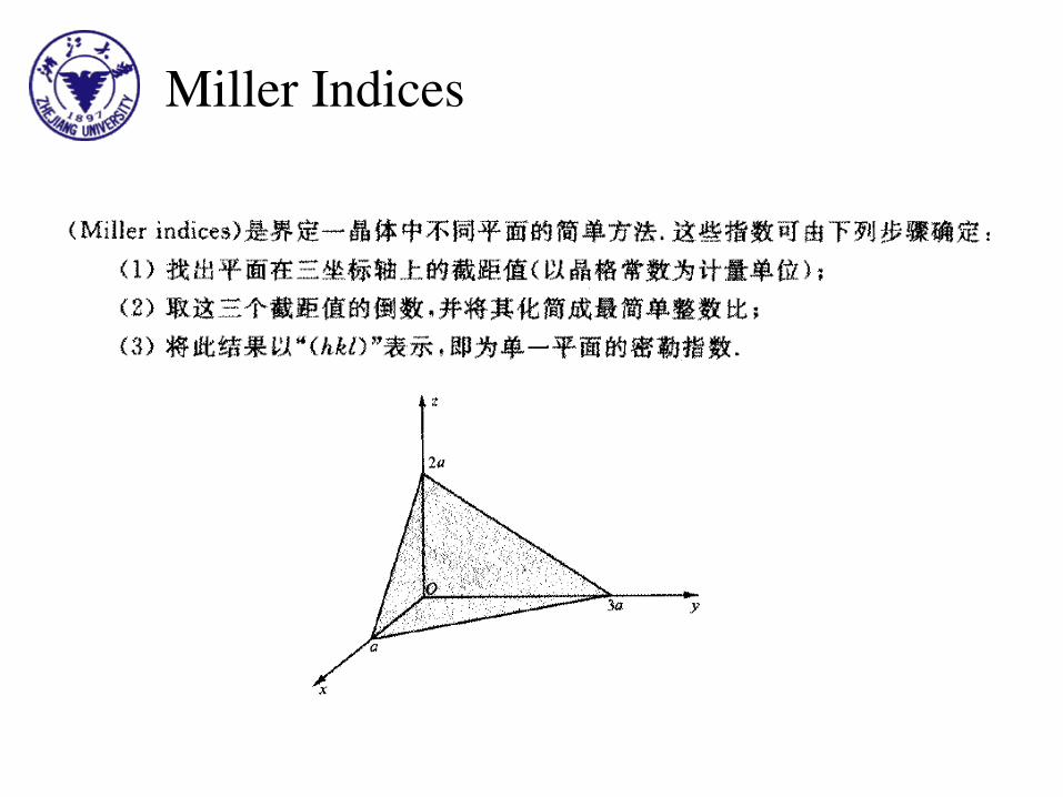
Miller Indices
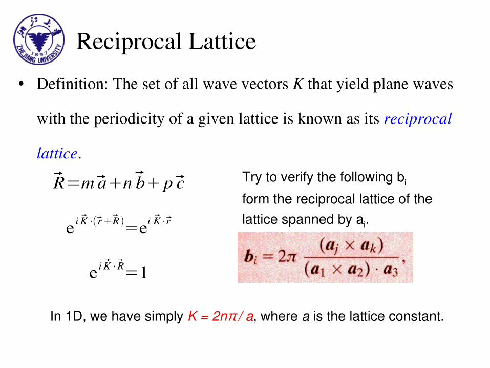
Reciprocal Lattice• Definition: The set of all wave vectors K that yield plane waves
with the periodicity of a given lattice is known as its reciprocal
lattice.Try to verify the following bi form the reciprocal lattice of the lattice spanned by ai.
In 1D, we have simply K = 2nπ / a, where a is the lattice constant.
R=manbpc
e i K⋅rR =ei K⋅r
e i K⋅R=1
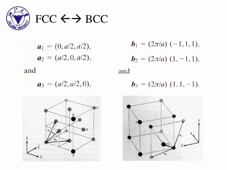
FCC BCC
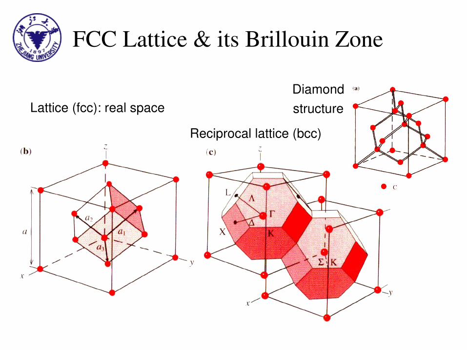
FCC Lattice & its Brillouin Zone
Lattice (fcc): real space
Reciprocal lattice (bcc)
Diamond structure
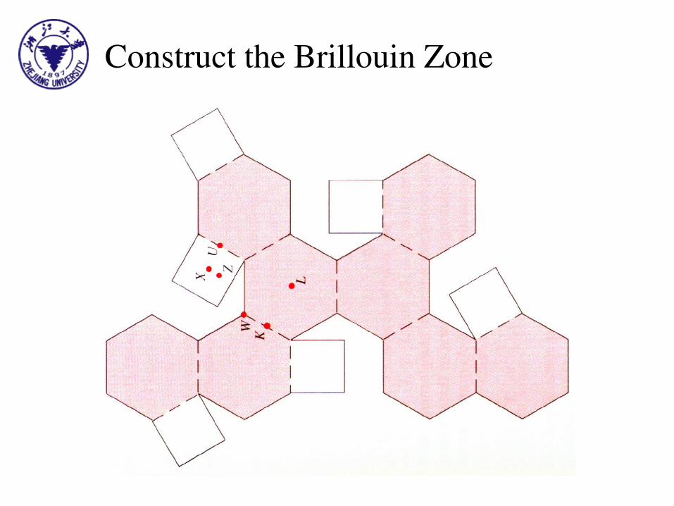
Construct the Brillouin Zone
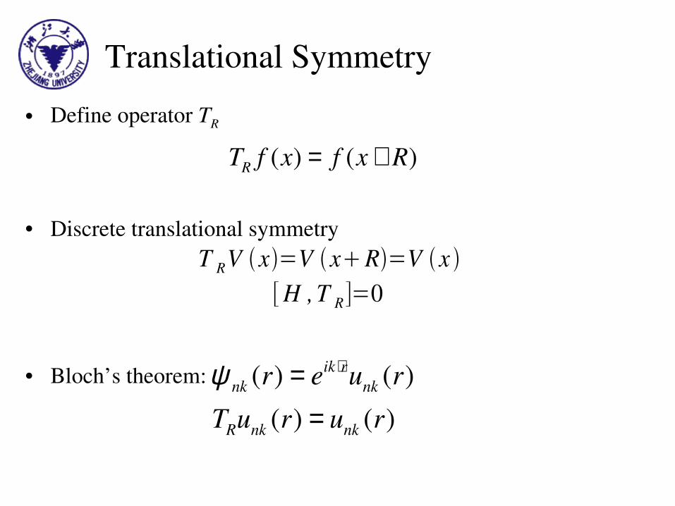
Translational Symmetry• Define operator TR
• Discrete translational symmetry
• Bloch’s theorem:
( ) ( )RT f x f x R= +
( ) ( )( ) ( )
ik rnk nk
R nk nk
r e u rT u r u rψ ∠=
=
T RV x=V xR=V x [H , T R]=0
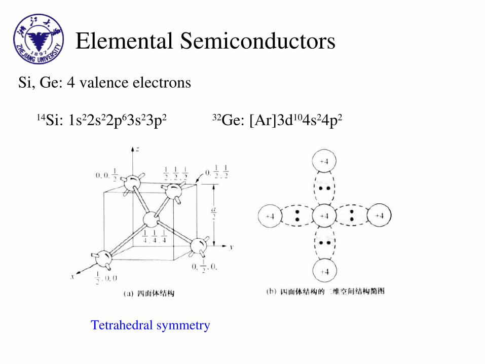
Elemental SemiconductorsSi, Ge: 4 valence electrons
14Si: 1s22s22p63s23p2 32Ge: [Ar]3d104s24p2
Tetrahedral symmetry
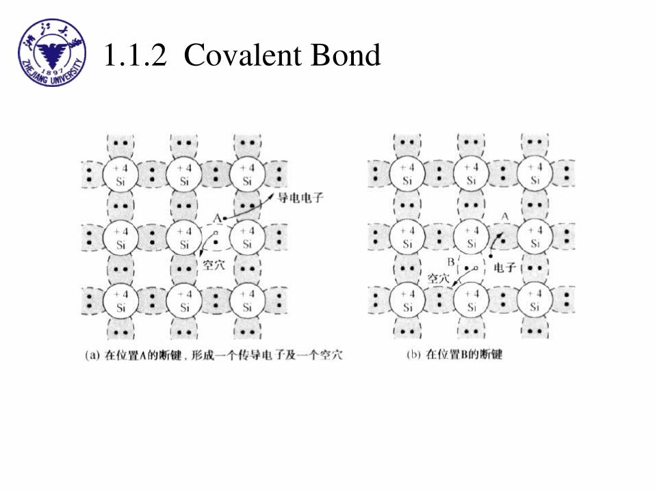
1.1.2 Covalent Bond
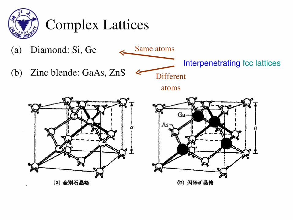
Complex Lattices(a) Diamond: Si, Ge
(b) Zinc blende: GaAs, ZnSInterpenetrating fcc lattices
Same atoms
Different atoms
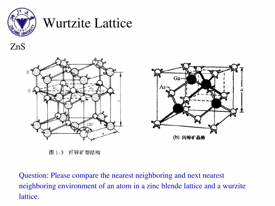
Wurtzite LatticeZnS
Question: Please compare the nearest neighboring and next nearest neighboring environment of an atom in a zinc blende lattice and a wurzite lattice.
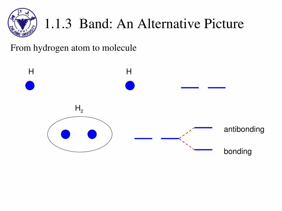
1.1.3 Band: An Alternative PictureFrom hydrogen atom to molecule
H H
H2
bonding
antibonding
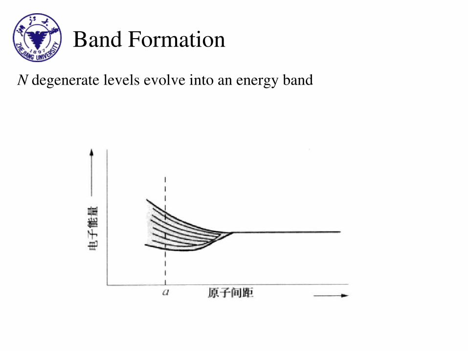
Band FormationN degenerate levels evolve into an energy band
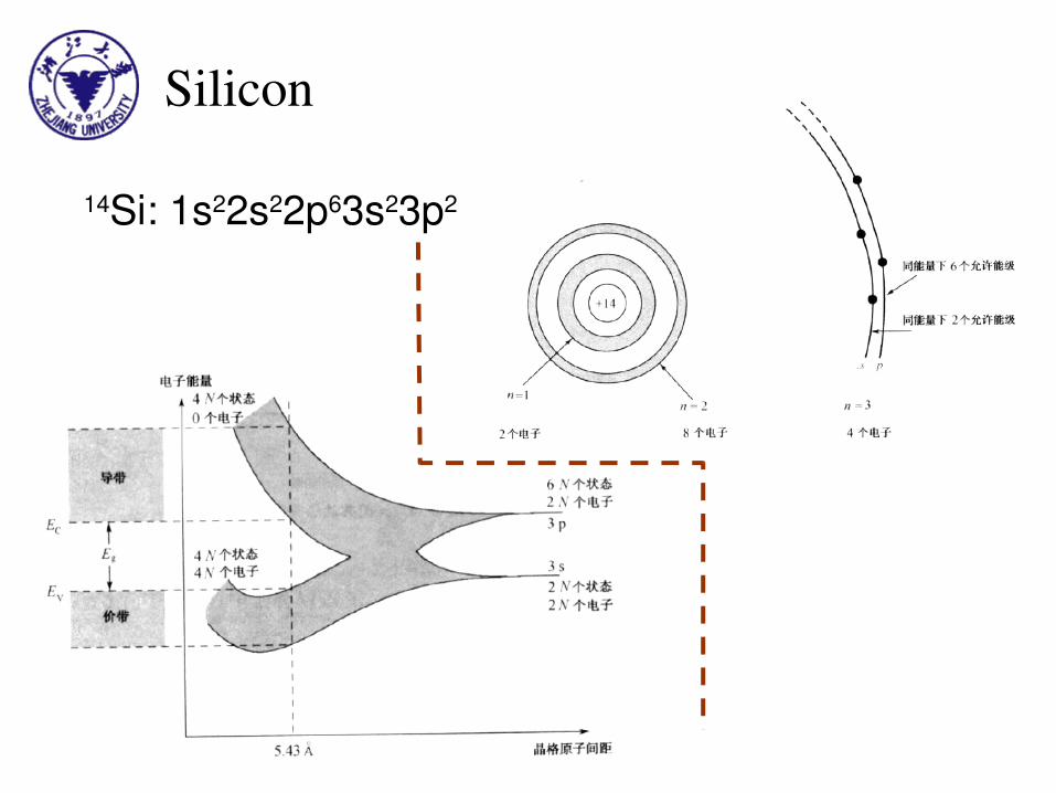
Silicon
14Si: 1s22s22p63s23p2

ResistivityConduction band, valence band & band gap
constant ,T 0 ∞ ,T 0
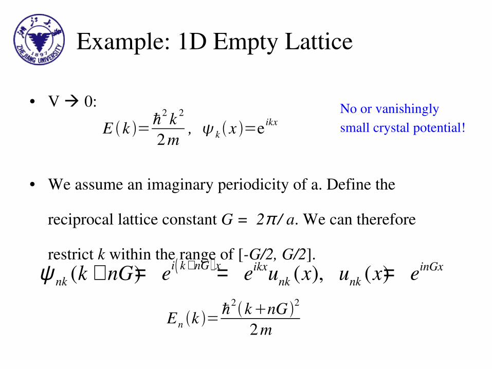
Example: 1D Empty Lattice
( )( ) ( ), ( )i k nG x ikx inGxnk nk nkk nG e e u x u x eψ ++ = = =
• V 0:
• We assume an imaginary periodicity of a. Define the
reciprocal lattice constant G = 2π / a. We can therefore
restrict k within the range of [G/2, G/2].
No or vanishingly small crystal potential!
En k =ℏ
2knG
2
2 m
E k =ℏ2 k 2
2 m , k x =e ikx
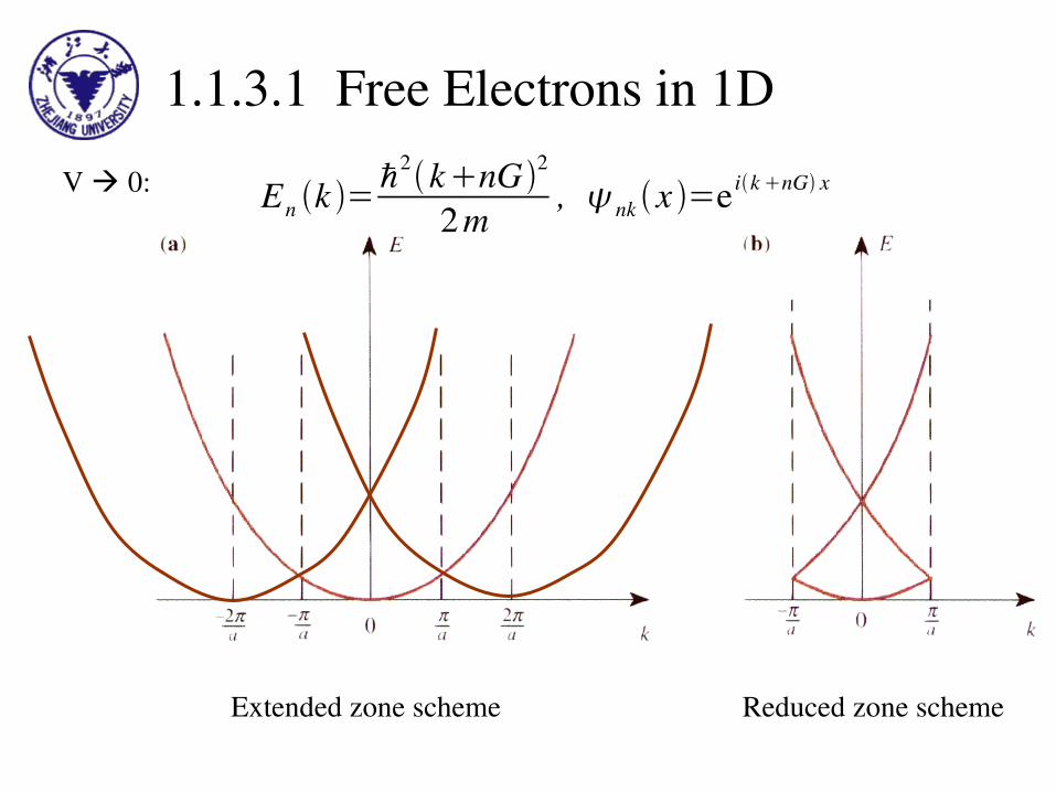
1.1.3.1 Free Electrons in 1DV 0:
Extended zone scheme Reduced zone scheme
En k =ℏ
2knG
2
2 m , nk x =e iknG x

Comments• The wave vector k is not momentum p/ħ, since Hamiltonian does
not have complete translational invariance. Rather, ħk is known as
crystal momentum (quantum number characteristic of the
translational symmetry of a periodic potential).
• The wave vector k can be confined to the first Brillouin zone.
• More in A/M Chapter 8.
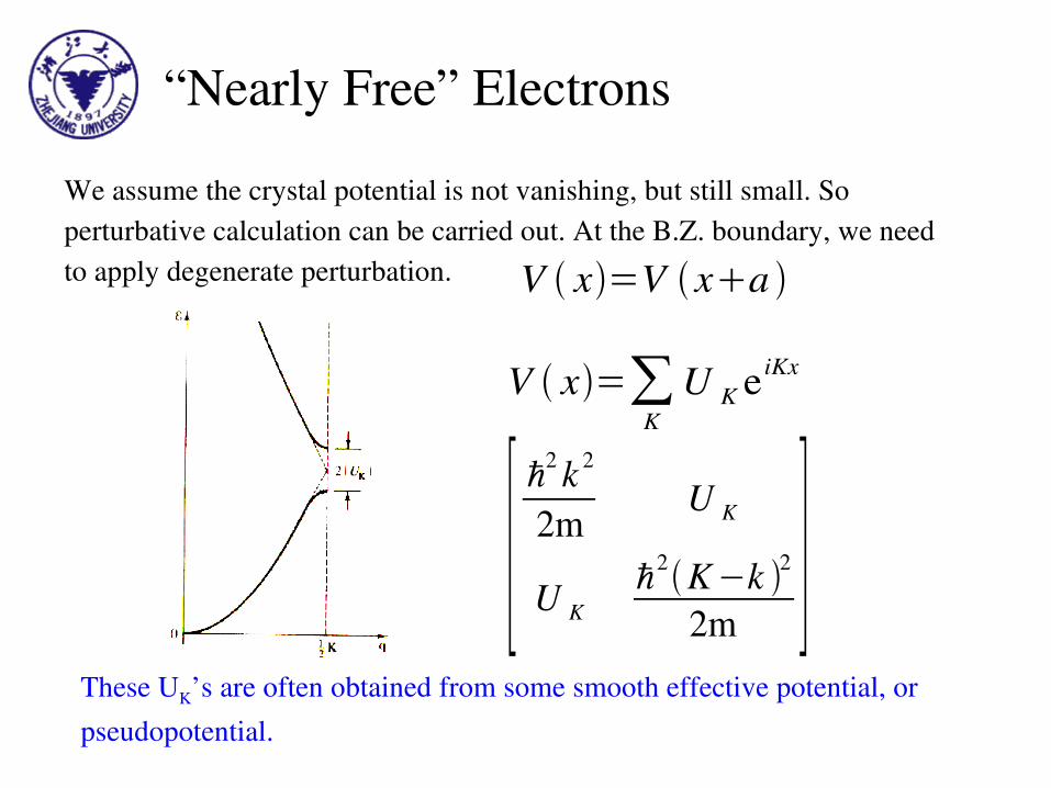
“Nearly Free” Electrons
We assume the crystal potential is not vanishing, but still small. So perturbative calculation can be carried out. At the B.Z. boundary, we need to apply degenerate perturbation.
These UK’s are often obtained from some smooth effective potential, or pseudopotential.
V x=V xa
V x=∑K
U K e iKx
[ℏ
2 k 2
2m U K
U Kℏ
2K−k 2
2m ]
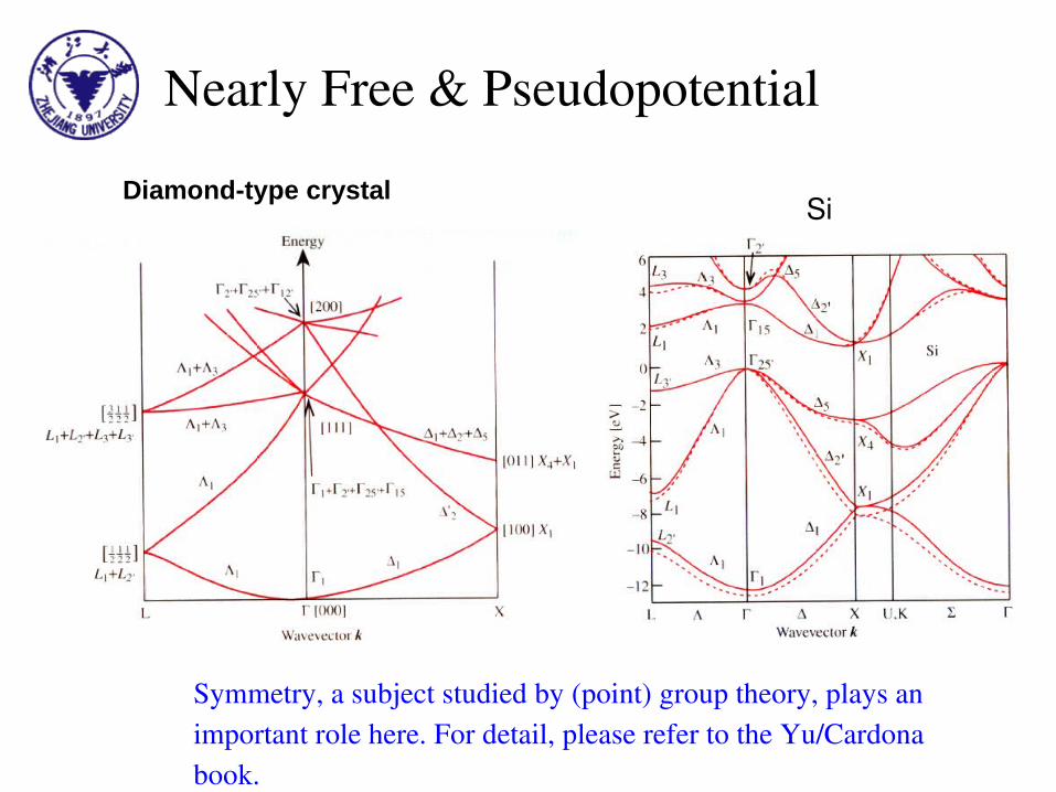
Nearly Free & Pseudopotential
SiDiamondtype crystal
Symmetry, a subject studied by (point) group theory, plays an important role here. For detail, please refer to the Yu/Cardona book.
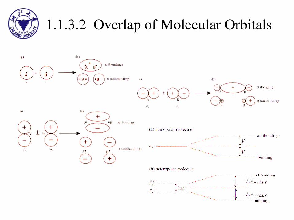
1.1.3.2 Overlap of Molecular Orbitals
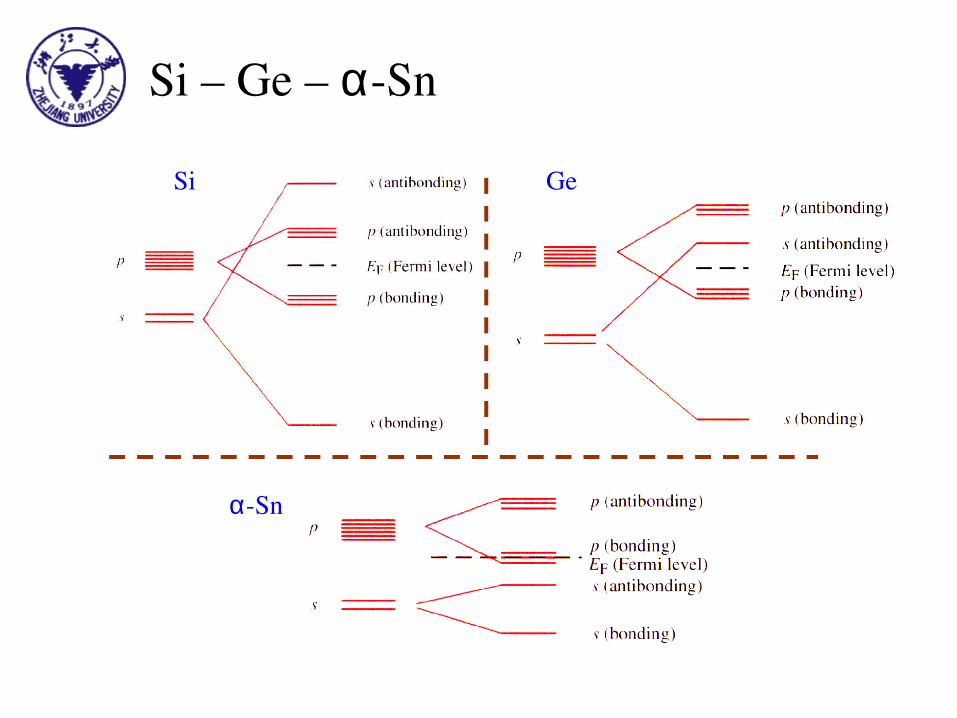
Si – Ge – αSn
Si Ge
αSn

ComparisonNearly free e’s + pseudopotential
• Electrons nearly free
• Wave functions approximated by
plane waves
• Electrons in conduction band are
delocalized, so can be approximated
well by nearly free electrons
Tightbinding or LCMO approach
• e’s tightly bound to nuclei
• Linear combination of atomic wave
functions
• Valence electrons are concentrated
mainly in the bonds and so they
retain more of their atomic
character.
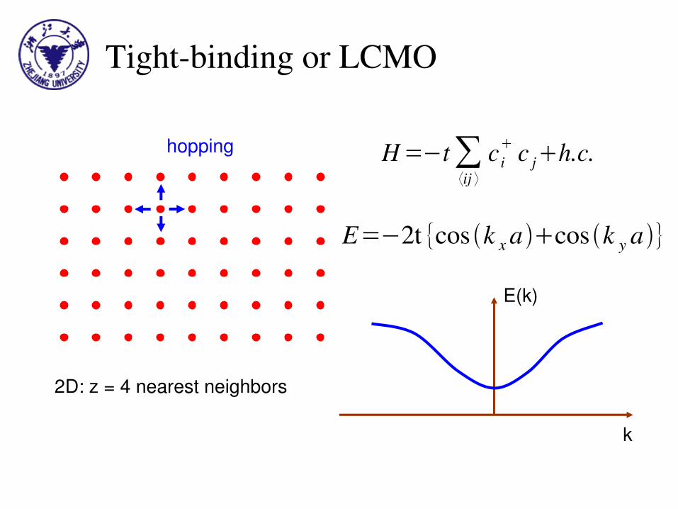
Tightbinding or LCMO
hopping
E(k)
k
2D: z = 4 nearest neighbors
H=−t∑⟨ij ⟩
c i c jh.c.
E=−2t {cos k x acos k y a}
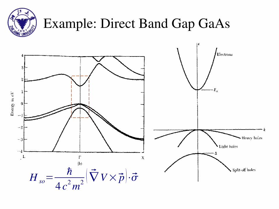
Example: Direct Band Gap GaAs
H so=ℏ
4 c2 m2 ∇V×p ⋅
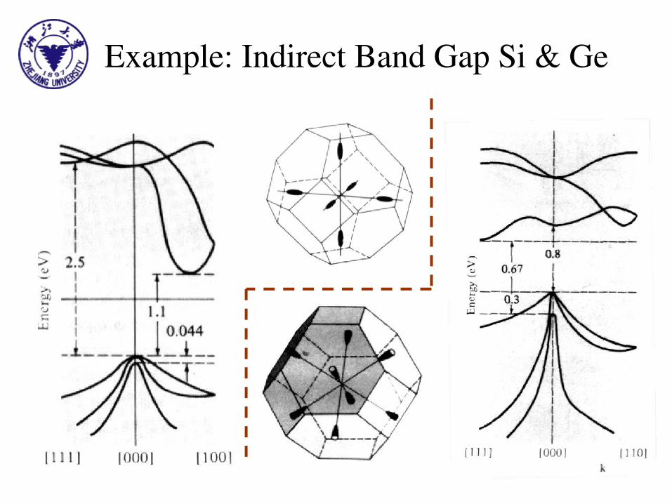
Example: Indirect Band Gap Si & Ge
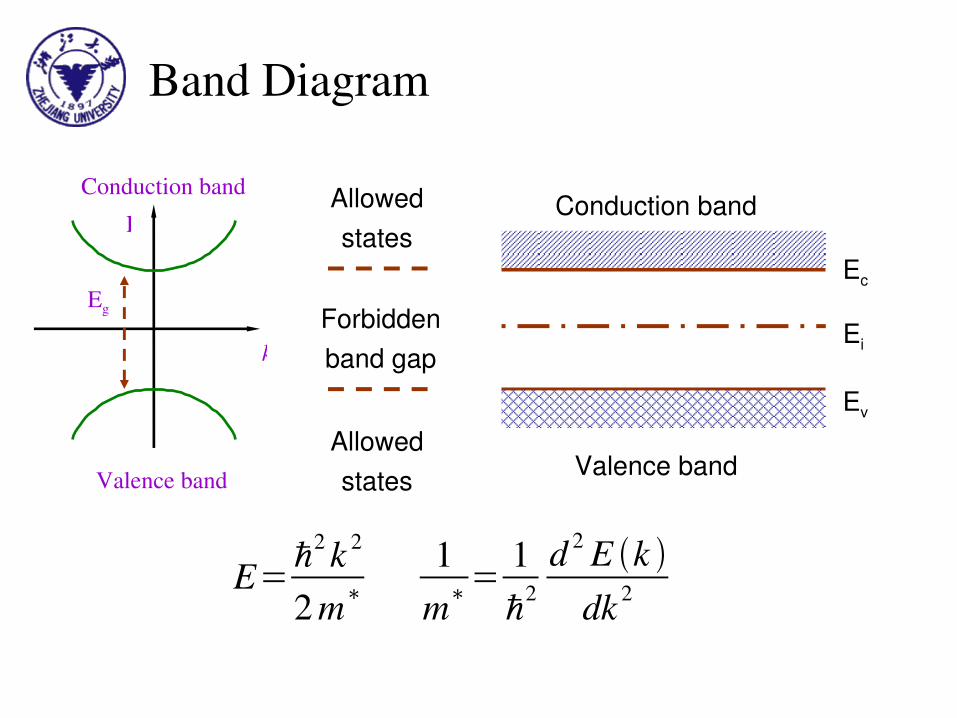
Band Diagram
Conduction band
Valence band
E
k
Conduction band
Valence band
Allowed states
Allowed states
Forbidden band gap
Ec
Ei
Ev
Eg
E=ℏ2 k 2
2 m∗
1m∗
=1ℏ
2d 2 E k
dk 2
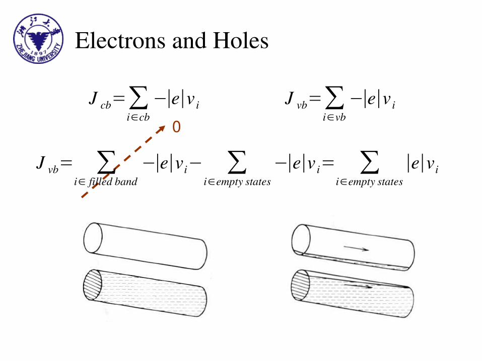
Electrons and Holes
0J cb=∑
i∈cb−∣e∣v i J vb=∑
i∈vb−∣e∣v i
J vb= ∑i∈ filled band
−∣e∣vi− ∑i∈empty states
−∣e∣v i= ∑i∈empty states
∣e∣vi
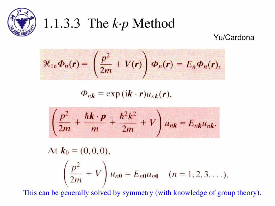
1.1.3.3 The k∙p MethodYu/Cardona
This can be generally solved by symmetry (with knowledge of group theory).
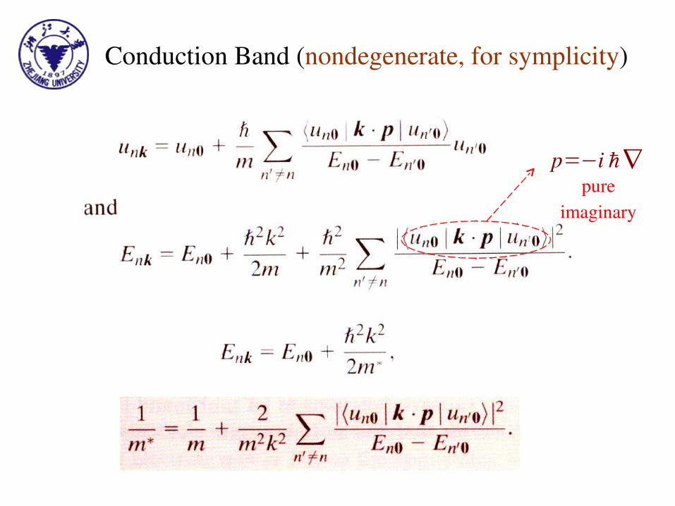
Conduction Band (nondegenerate, for symplicity)
pure imaginary
p=−i ℏ∇
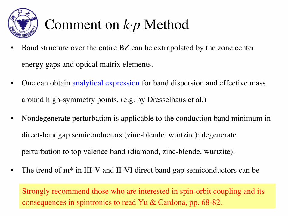
Comment on k∙p Method• Band structure over the entire BZ can be extrapolated by the zone center
energy gaps and optical matrix elements.
• One can obtain analytical expression for band dispersion and effective mass
around highsymmetry points. (e.g. by Dresselhaus et al.)
• Nondegenerate perturbation is applicable to the conduction band minimum in
directbandgap semiconductors (zincblende, wurtzite); degenerate
perturbation to top valence band (diamond, zincblende, wurtzite).
• The trend of m* in IIIV and IIVI direct band gap semiconductors can be
explained.Strongly recommend those who are interested in spinorbit coupling and its consequences in spintronics to read Yu & Cardona, pp. 6882.
Chapter 1. Fundamentals1.1 Bonds and bands
1.2 Impurities and defects
– Classification of defects
– Point defects
– Shallow (hydrogenic) impurities
– Heavy doping
1.3 Statistical distribution of charge carriers
1.4 Charge transport
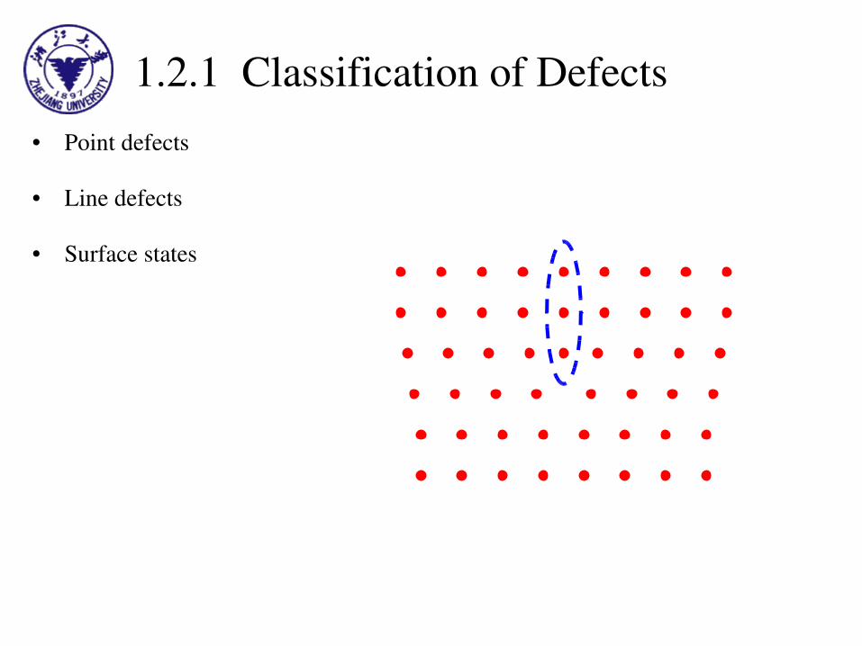
1.2.1 Classification of Defects• Point defects
• Line defects
• Surface states
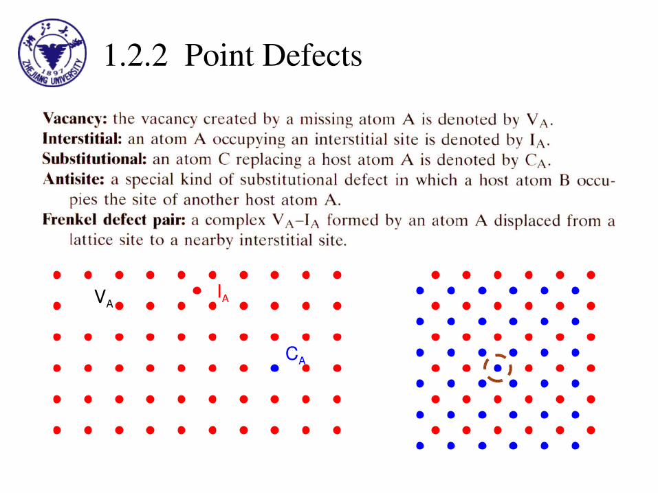
1.2.2 Point Defects
VAIA
CA
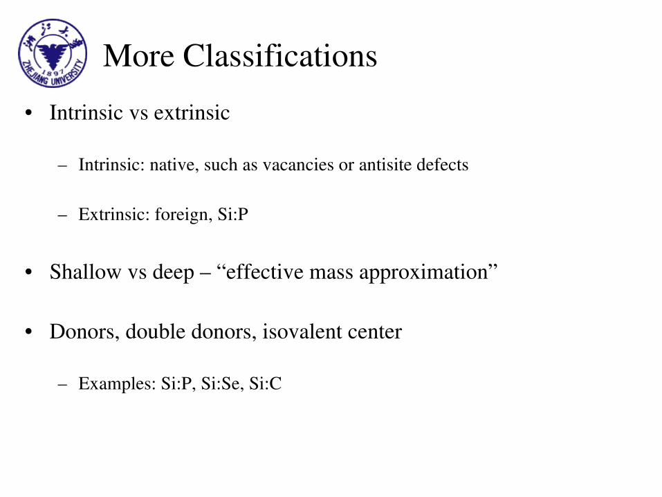
More Classifications• Intrinsic vs extrinsic
– Intrinsic: native, such as vacancies or antisite defects
– Extrinsic: foreign, Si:P
• Shallow vs deep – “effective mass approximation”
• Donors, double donors, isovalent center
– Examples: Si:P, Si:Se, Si:C

1.2.3 Shallow Impurity States
reHH cryst ε
2
−= impurity potential
TeSbSnInCd
SeAsGeGaZn
SPSiAl
ONCB
Si:P
Effective mass approximation
• Break translational symmetry
• No Bloch’s theorem!?
Screened Coulomb potential
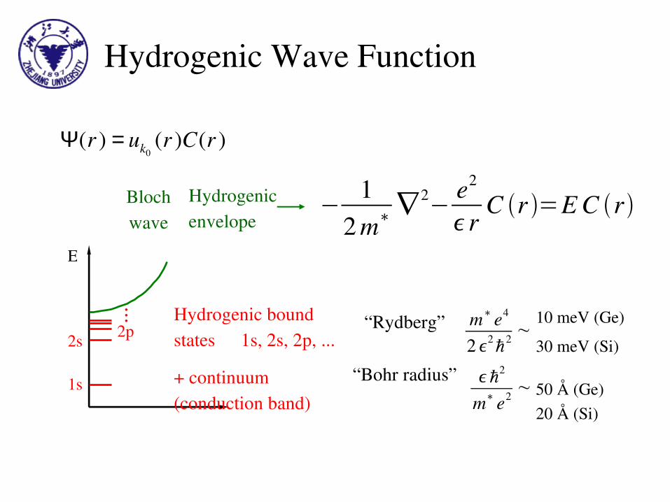
Hydrogenic Wave Function
1s
E
2s 2p
...
0( ) ( ) ( )kr u r C rΨ =
Bloch wave
Hydrogenic envelope
Hydrogenic bound states 1s, 2s, 2p, ...
+ continuum (conduction band)
“Rydberg”
“Bohr radius”
10 meV (Ge)
30 meV (Si)
50 Å (Ge)20 Å (Si)
−1
2 m∗∇
2−
e2
r C r =E C r
ℏ2
m∗ e2 ~
m∗ e4
2 2ℏ2 ~
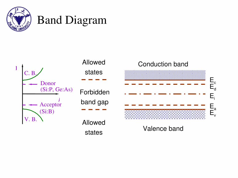
Band Diagram
Donor (Si:P, Ge:As)
C. B.
V. B.
Acceptor (Si:B)
E
k
Conduction band
Valence band
Allowed states
Allowed states
Forbidden band gap
EcEd
Ei
EaEv
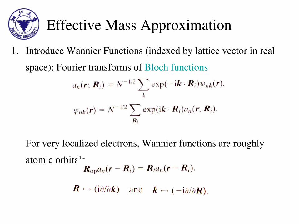
Effective Mass Approximation1. Introduce Wannier Functions (indexed by lattice vector in real
space): Fourier transforms of Bloch functions
For very localized electrons, Wannier functions are roughly atomic orbitals.
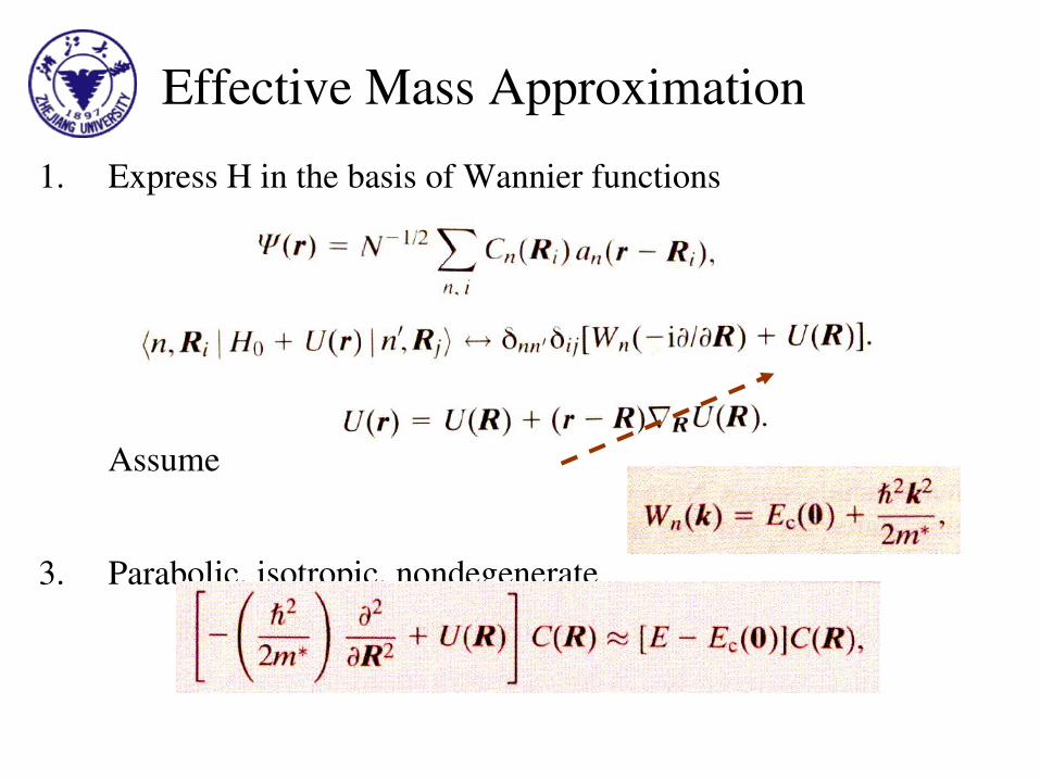
Effective Mass Approximation1. Express H in the basis of Wannier functions
Assume
3. Parabolic, isotropic, nondegenerate
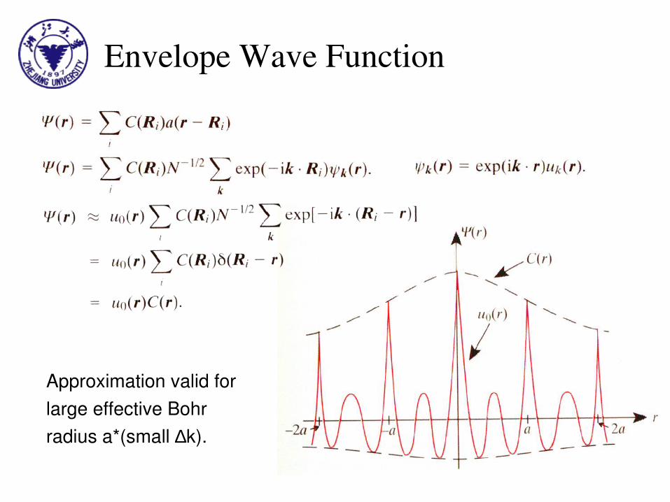
Envelope Wave Function
Approximation valid for large effective Bohr radius a*(small ∆k).
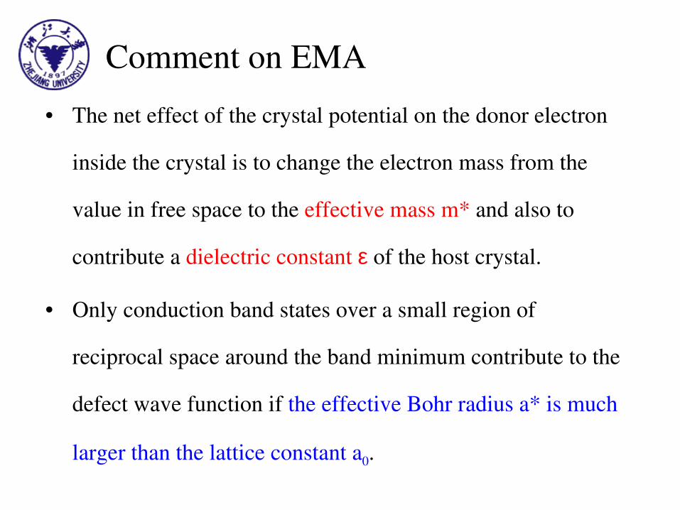
Comment on EMA• The net effect of the crystal potential on the donor electron
inside the crystal is to change the electron mass from the
value in free space to the effective mass m* and also to
contribute a dielectric constant ε of the host crystal.
• Only conduction band states over a small region of
reciprocal space around the band minimum contribute to the
defect wave function if the effective Bohr radius a* is much
larger than the lattice constant a0.

1.2.4 Heavy Doping• Light doping: impurity atoms
do not interact with each
other impurity level
• Heavy doping: perturb the
band structure of the host
crystal reduction of
bandgap
E
ρ(E)
EcEd
Ev
Eg
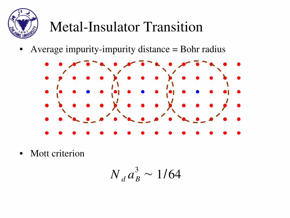
MetalInsulator Transition• Average impurityimpurity distance = Bohr radius
• Mott criterion
N d aB3 ~ 1/64
Chapter 1. Fundamentals1.1 Bonds and bands
1.2 Impurities and defects
1.3 Statistical distribution of charge carriers
– Thermal equilibrium
– Massaction law
– Fermi level
1.4 Charge transport
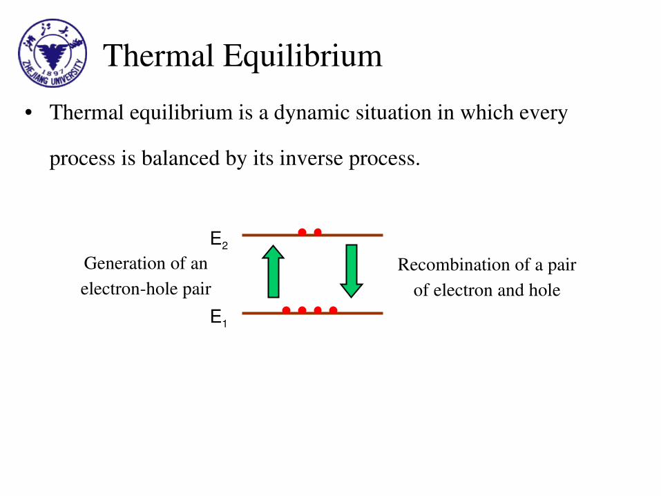
Thermal Equilibrium• Thermal equilibrium is a dynamic situation in which every
process is balanced by its inverse process.
E1
E2
Generation of an electronhole pair
Recombination of a pair of electron and hole
MassAction Law
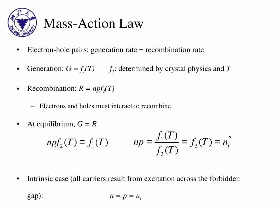
• Electronhole pairs: generation rate = recombination rate
• Generation: G = f1(T) f1: determined by crystal physics and T
• Recombination: R = npf2(T)
– Electrons and holes must interact to recombine
• At equilibrium, G = R
• Intrinsic case (all carriers result from excitation across the forbidden
gap): n = p = ni
2 1( ) ( )npf T f T= 213
2
( ) ( )( ) i
f Tnp f T nf T
= = =
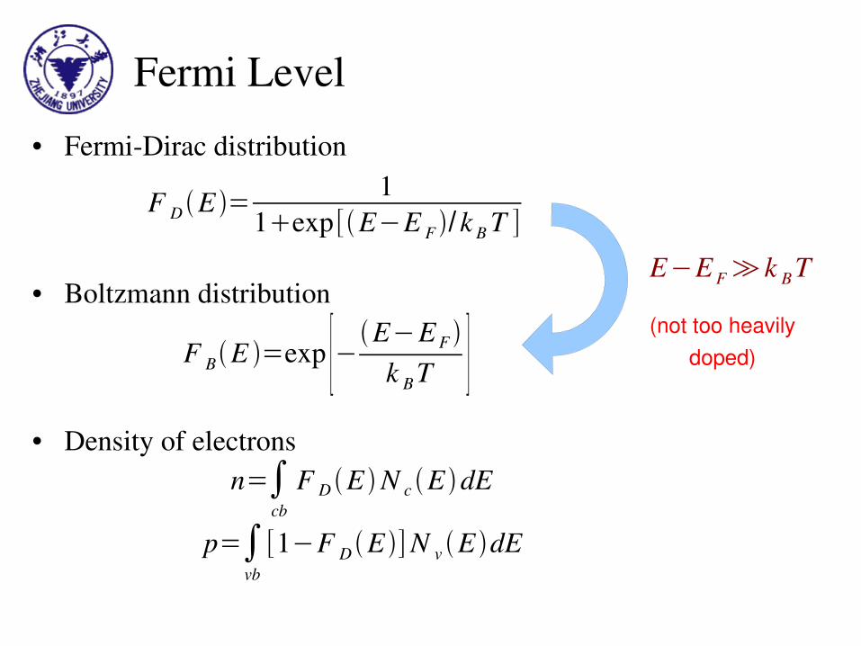
Fermi Level• FermiDirac distribution
• Boltzmann distribution
• Density of electrons
(not too heavily doped)
E−E F≫k B T
F D E =1
1exp [E−E F /k B T ]
F BE =exp [−E−E F
k B T ]
n=∫cb
F D E N c E dE
p=∫vb[1−F D E ]N v E dE
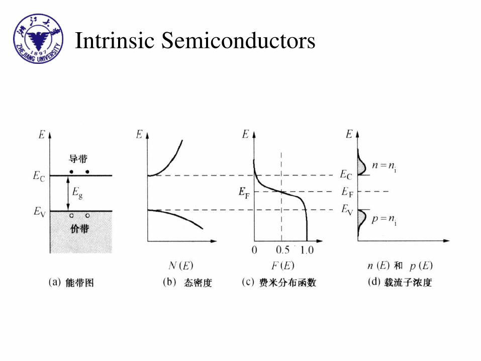
Intrinsic Semiconductors
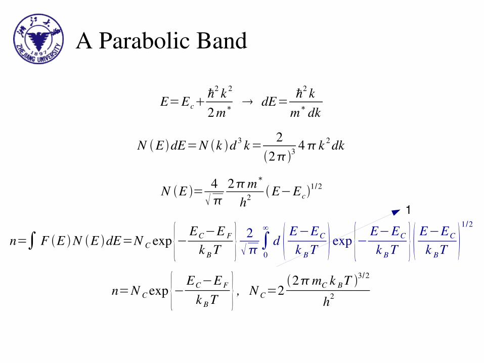
A Parabolic Band
E=Ecℏ2 k 2
2 m∗ dE= ℏ2 k
m∗dk
N E dE=N k d 3 k= 223
4 k 2 dk
N E = 4
2m∗
h2 E−Ec1/2
n=∫ F E N E dE=N C exp {−EC−E F
k B T } 2∫0
∞
d E−EC
k B T exp {− E−EC
k B T } E−EC
k BT 1/2
n=N C exp {−EC−E F
k B T } , N C=22mC k BT 3/2
h2
1
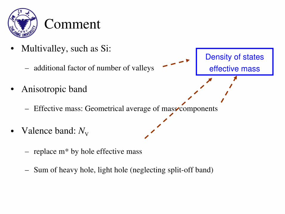
Comment• Multivalley, such as Si:
– additional factor of number of valleys
• Anisotropic band
– Effective mass: Geometrical average of mass components
• Valence band: NV
– replace m* by hole effective mass
– Sum of heavy hole, light hole (neglecting splitoff band)
Density of states effective mass

Intrinsic Carrier Concentration
n=N C exp {−EC−E F
k B T } , N C=22mC k B T 3/2
h2
n=N V exp {−E F−EV
k B T } , N V=22mV k B T 3/2
h2
ni2=np=N C N V exp {−EC−EV
k B T }=N C N V exp {− E g
k B T }
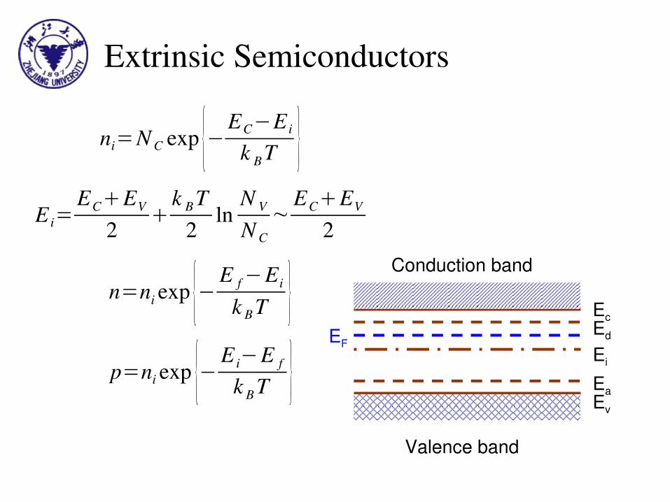
Extrinsic Semiconductors
Conduction band
Valence band
EcEd
Ei
EaEv
EF
ni=N C exp {−EC−E i
k B T }E i=
ECEV
2
k B T2
lnN V
N C~
ECEV
2
n=ni exp {−E f−Ei
k B T }p=ni exp {−E i−E f
k B T }

Doped Semiconductors• Assuming full ionization,
charge neutrality
• With intentional doping,
typically for ntype
• Majority carriers
• Minority carriers
• Compensation
N d p=N an
n− p=n−ni
2
n =N d−N a
n=N d−N a
2{ N d−N a
2 2
ni2 }
1/2
N d−N a≫ni
n=N d−N a
p=ni
2
N d−N a
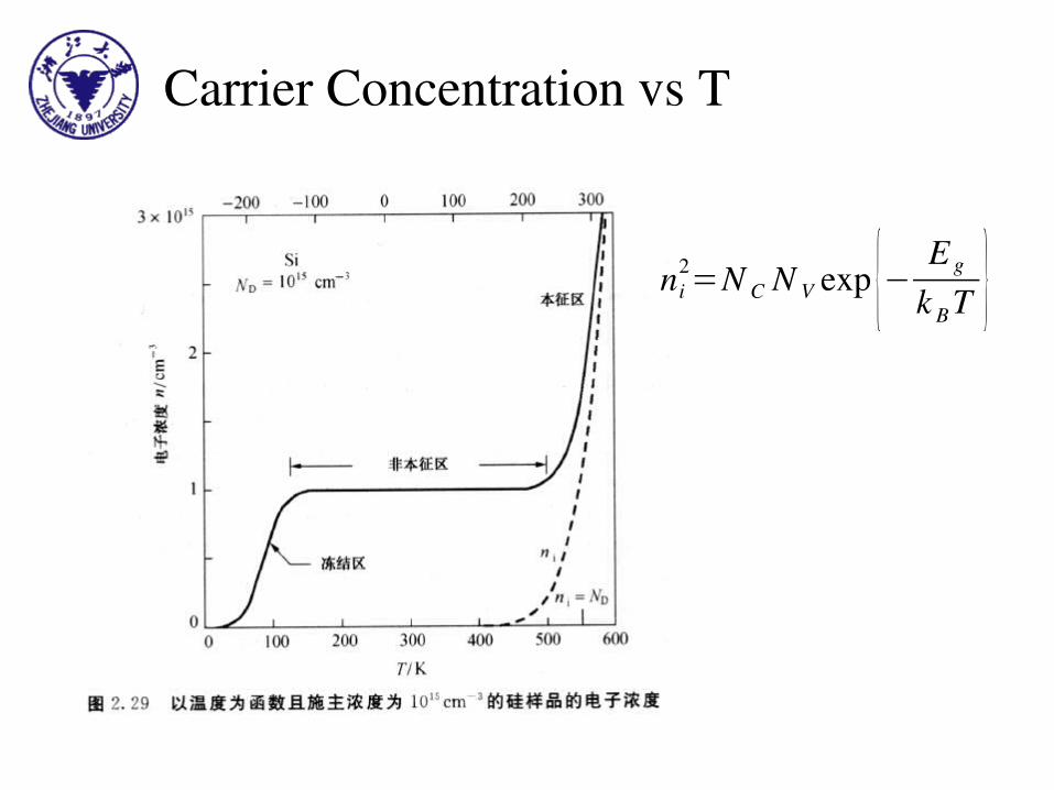
Carrier Concentration vs T
ni2=N C N V exp {− E g
k B T }
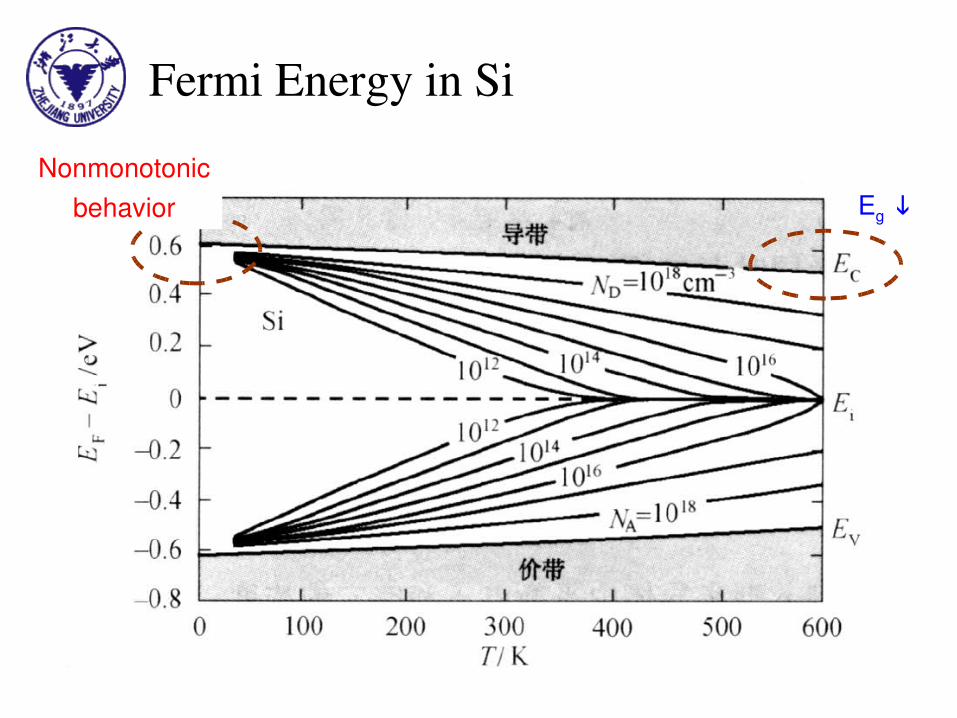
Fermi Energy in Si
Eg ↓Nonmonotonic
behavior
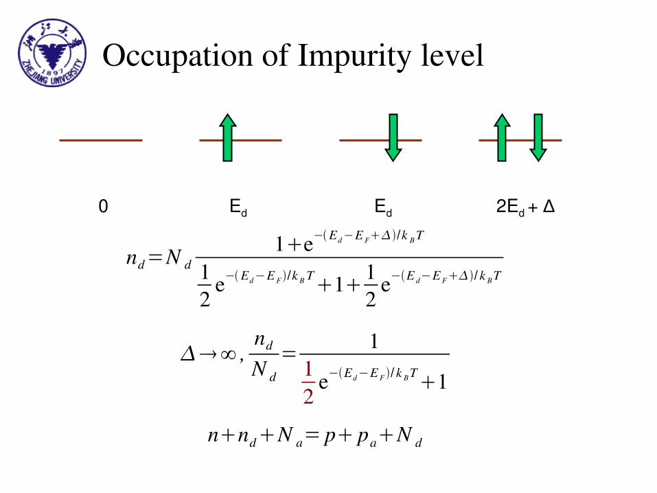
Occupation of Impurity level
0 Ed Ed 2Ed + ∆
nd=N d1e−Ed−E F/k B T
12
e−Ed−E F /k B T11
2e−E d−E F/ k B T
∞ ,nd
N d=
112 e−Ed−E F / k B T
1
nndN a= p paN d
Chapter 1. Fundamentals1.1 Bonds and bands
1.2 Impurities and defects
1.3 Statistical distribution of charge carriers
1.4 Charge transport
– Drift, diffusion, recombination, generation, thermionic emission,
tunneling, …
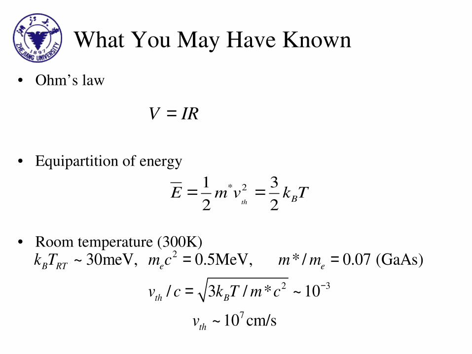
What You May Have Known• Ohm’s law
• Equipartition of energy
• Room temperature (300K)
V IR=
* 21 32 2th BE m v k T= =
2
2 3
7
~ 30meV, 0.5MeV, * / 0.07 (GaAs)
/ 3 / * ~ 10
~ 10 cm/s
B RT e e
th B
th
k T m c m m
v c k T m cv
−
= =
=
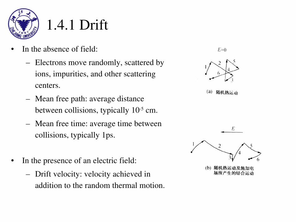
1.4.1 Drift• In the absence of field:
– Electrons move randomly, scattered by ions, impurities, and other scattering centers.
– Mean free path: average distance between collisions, typically 105 cm.
– Mean free time: average time between collisions, typically 1ps.
• In the presence of an electric field:– Drift velocity: velocity achieved in
addition to the random thermal motion.
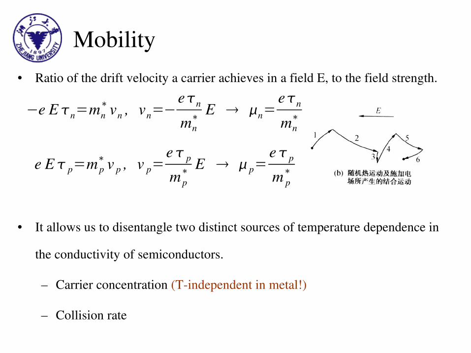
Mobility• Ratio of the drift velocity a carrier achieves in a field E, to the field strength.
• It allows us to disentangle two distinct sources of temperature dependence in
the conductivity of semiconductors.
– Carrier concentration (Tindependent in metal!)
– Collision rate
−e E n=mn∗vn , vn=−
en
mn∗
E n=en
mn∗
e E p=m p∗ v p , v p=
e p
m p∗
E p=ep
m p∗
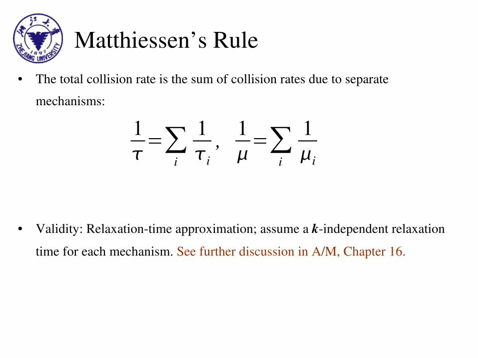
Matthiessen’s Rule• The total collision rate is the sum of collision rates due to separate
mechanisms:
• Validity: Relaxationtime approximation; assume a kindependent relaxation time for each mechanism. See further discussion in A/M, Chapter 16.
1=∑
i
1i
, 1=∑
i
1i
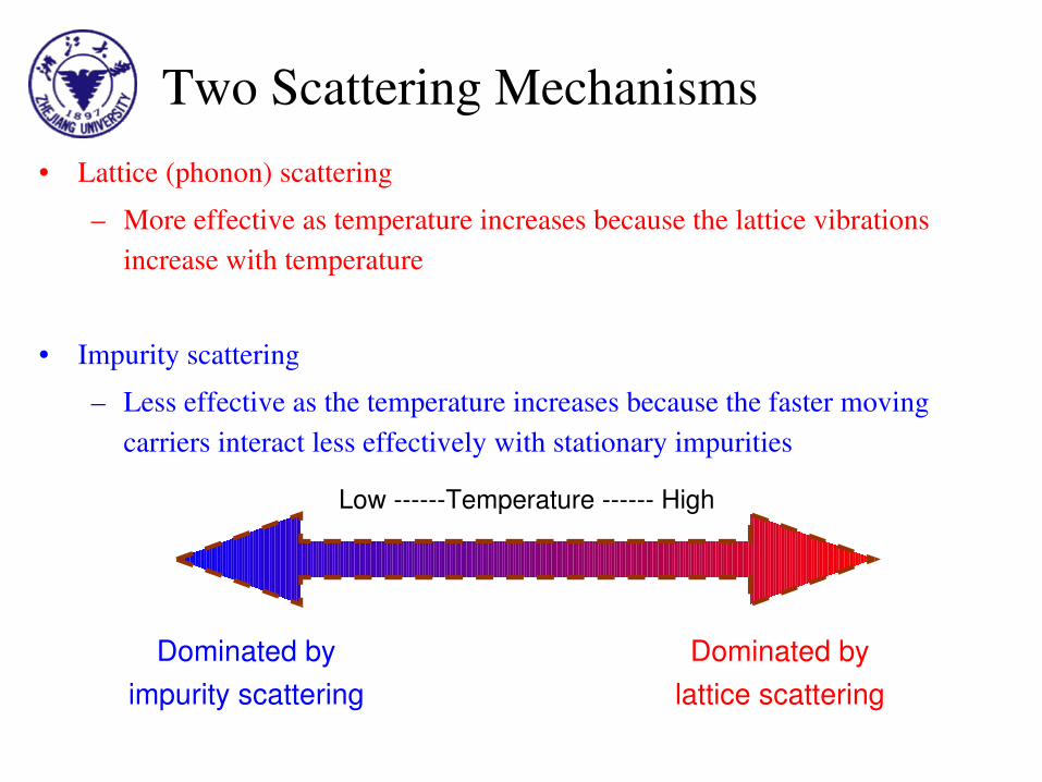
Two Scattering Mechanisms• Lattice (phonon) scattering
– More effective as temperature increases because the lattice vibrations increase with temperature
• Impurity scattering– Less effective as the temperature increases because the faster moving
carriers interact less effectively with stationary impurities
Dominated by impurity scattering
Dominated by lattice scattering
Low Temperature High
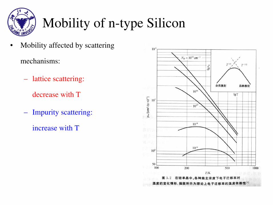
Mobility of ntype Silicon• Mobility affected by scattering
mechanisms:
– lattice scattering:
decrease with T
– Impurity scattering:
increase with T
Conductivity & Resistivity
( )1, 1
n p
n
p
pn p
n
ne
J J J ne pe E E
np
ee
peσ µ µ
σ
ρµ
µ µ
σ µ= = =
+
=
+
= + = +
J n=I n
A =∑i=1
n
−e vi =−n e vn=n en E
J p=I p
A =∑i=1
p
e vi =n e v p=n e p E
n=en
mn∗
, vn=−en
mn∗
E
p=e p
m p∗
, v p=e p
m p∗
E
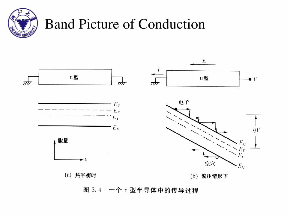
Band Picture of Conduction
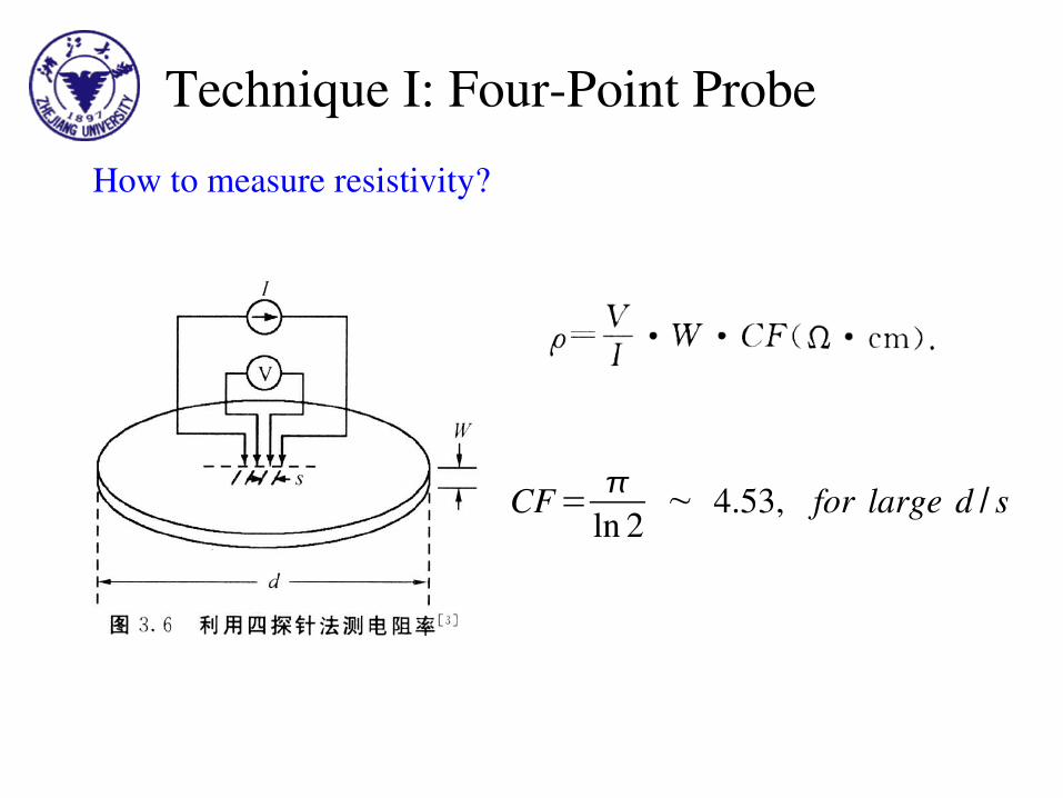
Technique I: FourPoint ProbeHow to measure resistivity?
CF=
ln 2~ 4.53, for large d / s
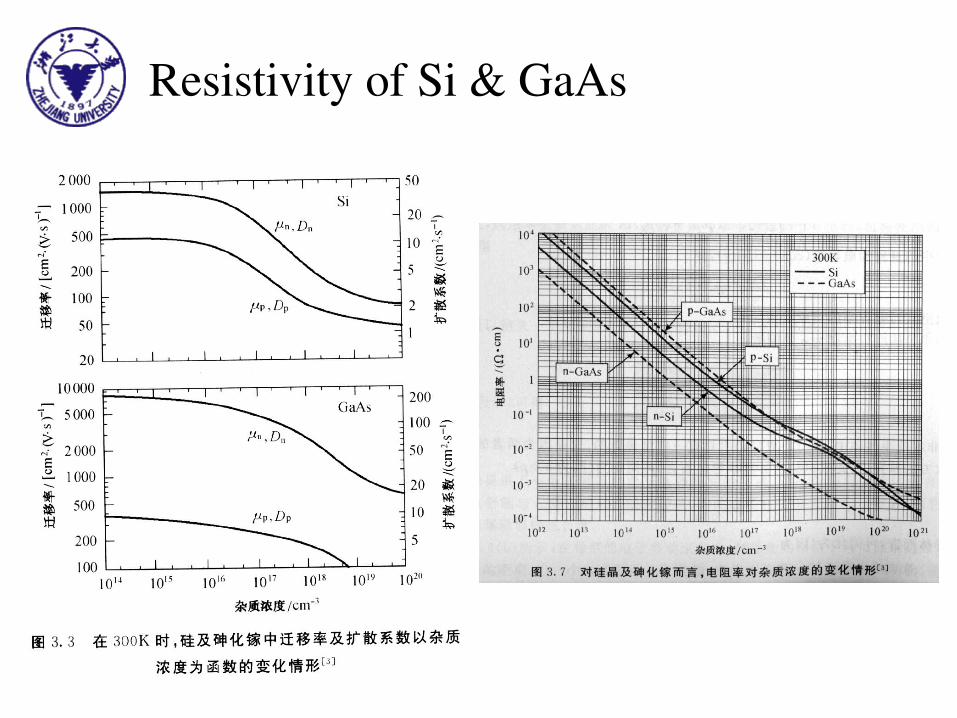
Resistivity of Si & GaAs

Technique II: Hall Effect• How to measure carrier type and concentration?
e E y=ev x
c B z E y=v x
c B z
E y=J p
p e c B z=RH J p B z
RH=1
p e c for holes
RH=−1n e c for electrons
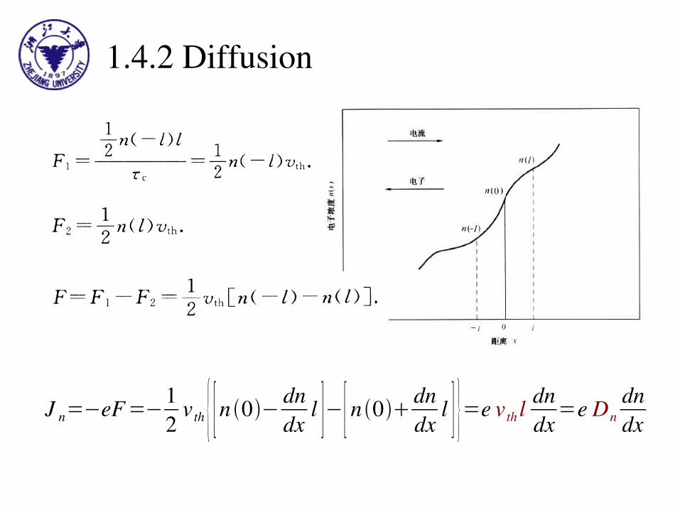
1.4.2 Diffusion
J n=−eF=−12
v th { [ n 0− dndx l ]−[ n 0 dn
dx l ] }=e v th l dndx=e Dn
dndx

Einstein Relation• Relates the two important constants that characterize freecarrier
transport by drift and by diffusion in a solid.
Dn=vth l=v th2 n
12
mn∗vth
2=
12
k B T Dn=k B T
e n
n=en
mn∗
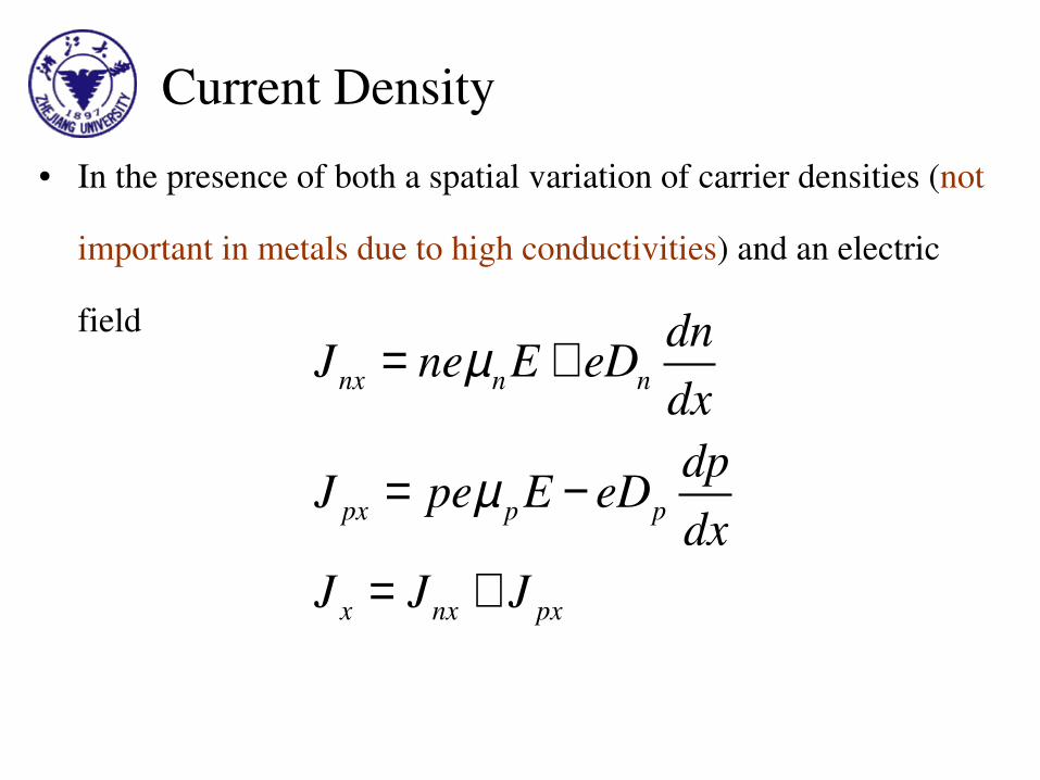
Current Density• In the presence of both a spatial variation of carrier densities (not
important in metals due to high conductivities) and an electric
field nx n n
px p p
x nx px
dnJ ne E eDdxdpJ pe E eDdx
J J J
µ
µ
= +
= −
= +
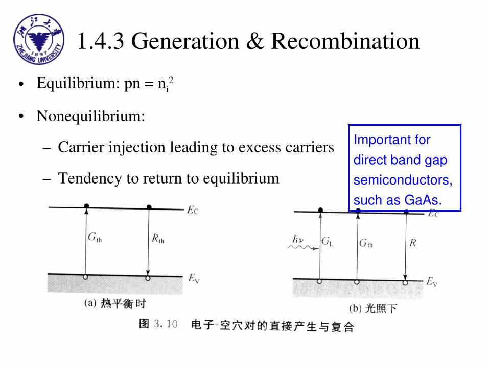
1.4.3 Generation & Recombination• Equilibrium: pn = ni
2
• Nonequilibrium:
– Carrier injection leading to excess carriers
– Tendency to return to equilibrium
Important for direct band gap semiconductors, such as GaAs.
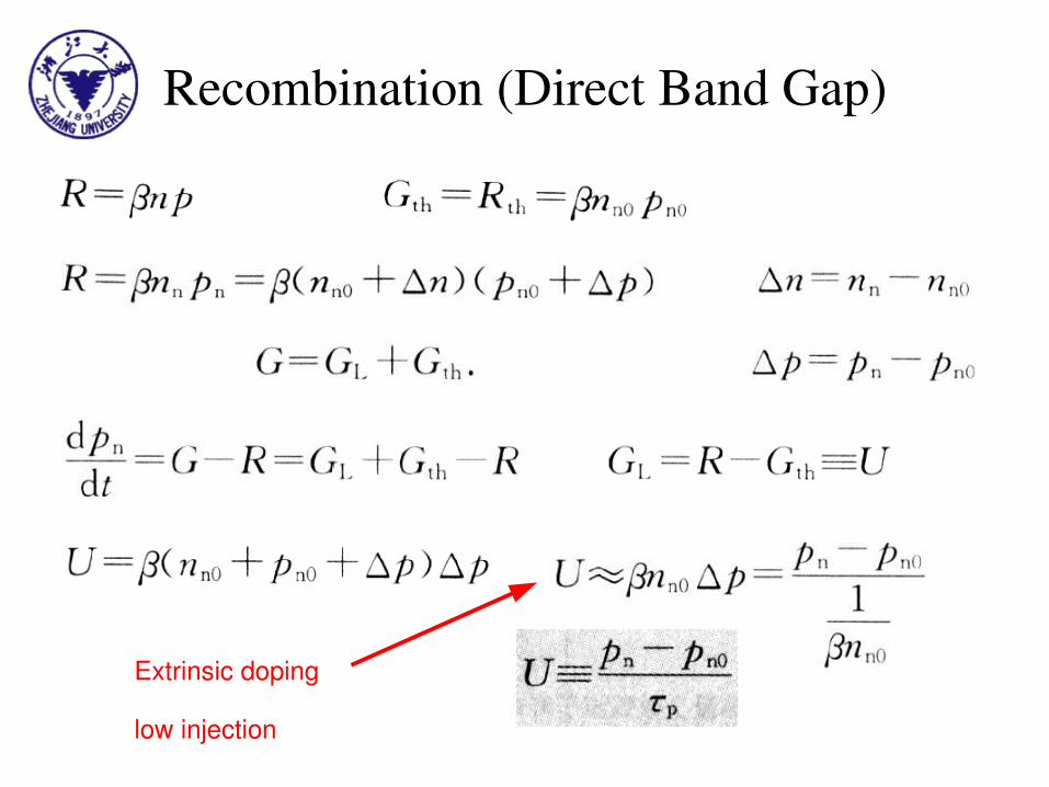
Recombination (Direct Band Gap)
Extrinsic doping
low injection
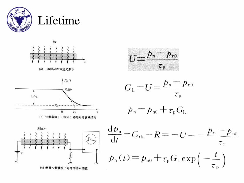
Lifetime
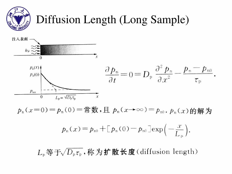
Diffusion Length (Long Sample)

Question: Short Sample
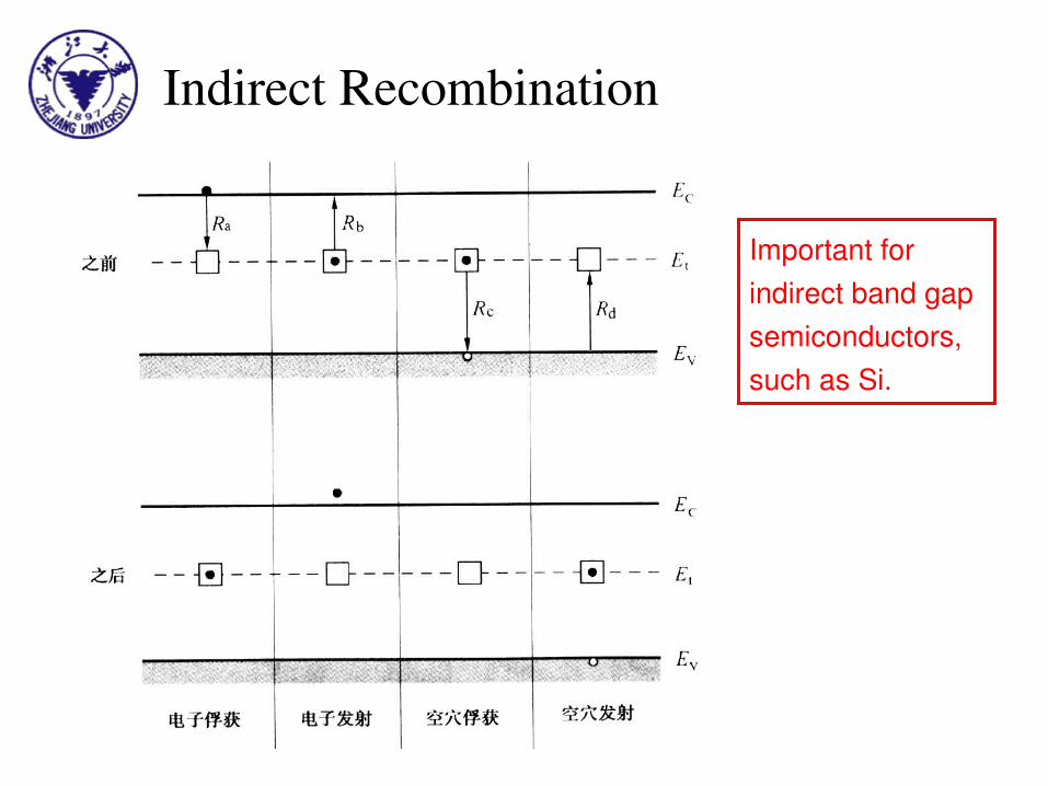
Indirect Recombination
Important for indirect band gap semiconductors, such as Si.
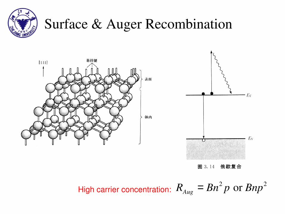
Surface & Auger Recombination
2 2 or AugR Bn p Bnp=High carrier concentration:
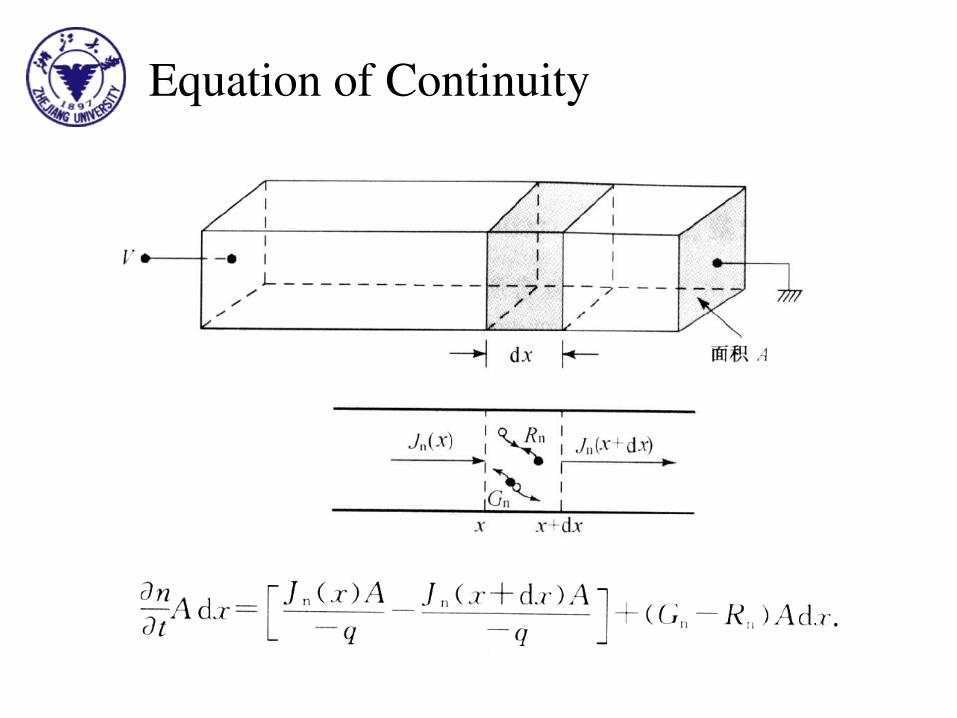
Equation of Continuity
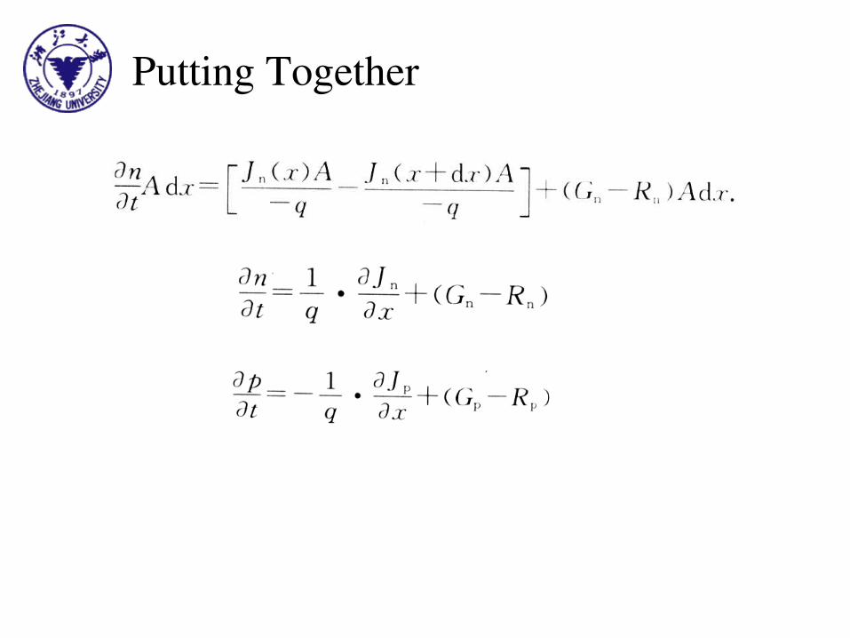
Putting Together
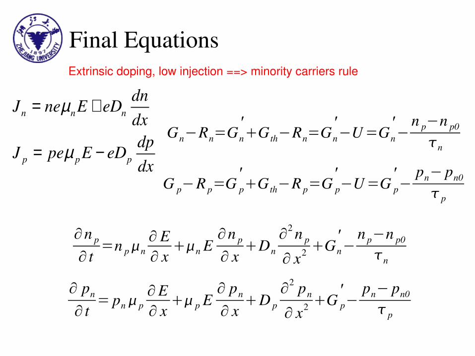
Final Equations
n n n
p p p
dnJ ne E eDdxdpJ pe E eDdx
µ
µ
= +
= −
∂n p
∂ t =n pn∂ E∂ x n E
∂n p
∂ x Dn∂
2 n p
∂ x2 Gn'−
n p−n p0
n
∂ pn
∂ t = pn p∂E∂ x p E
∂ pn
∂ x D p∂
2 pn
∂ x2 G p'−
pn− pn0
p
Extrinsic doping, low injection ==> minority carriers rule
Gn−Rn=Gn'G th−Rn=Gn
'−U=Gn
'−
n p−n p0
n
G p−R p=G p'G th−R p=G p
'−U=G p
'−
pn− pn0
p
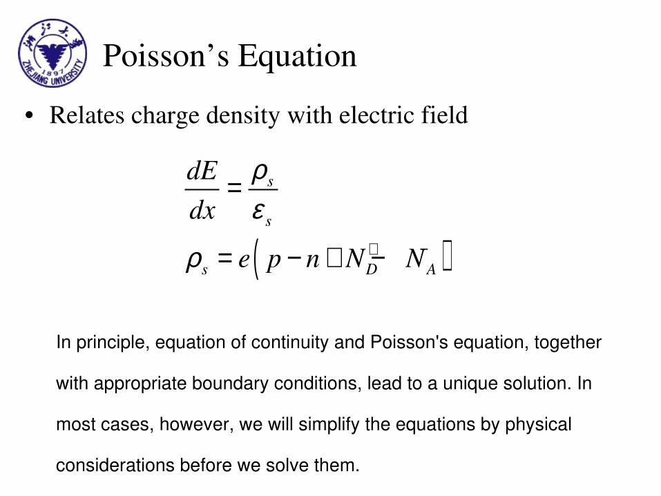
Poisson’s Equation
• Relates charge density with electric field
( )
s
s
s D A
dEdx
e p n N N
ρε
ρ + −
=
= − + −
In principle, equation of continuity and Poisson's equation, together
with appropriate boundary conditions, lead to a unique solution. In
most cases, however, we will simplify the equations by physical
considerations before we solve them.

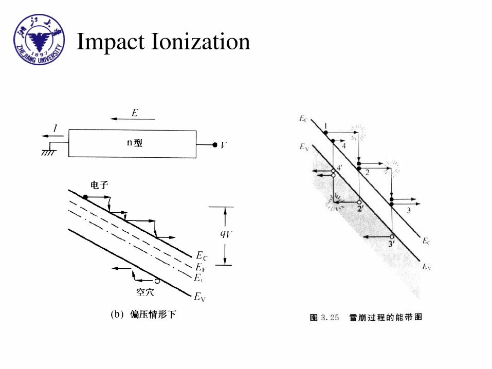
1.4.4 Thermionic Emission
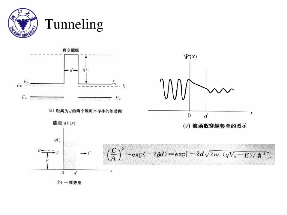
Tunneling
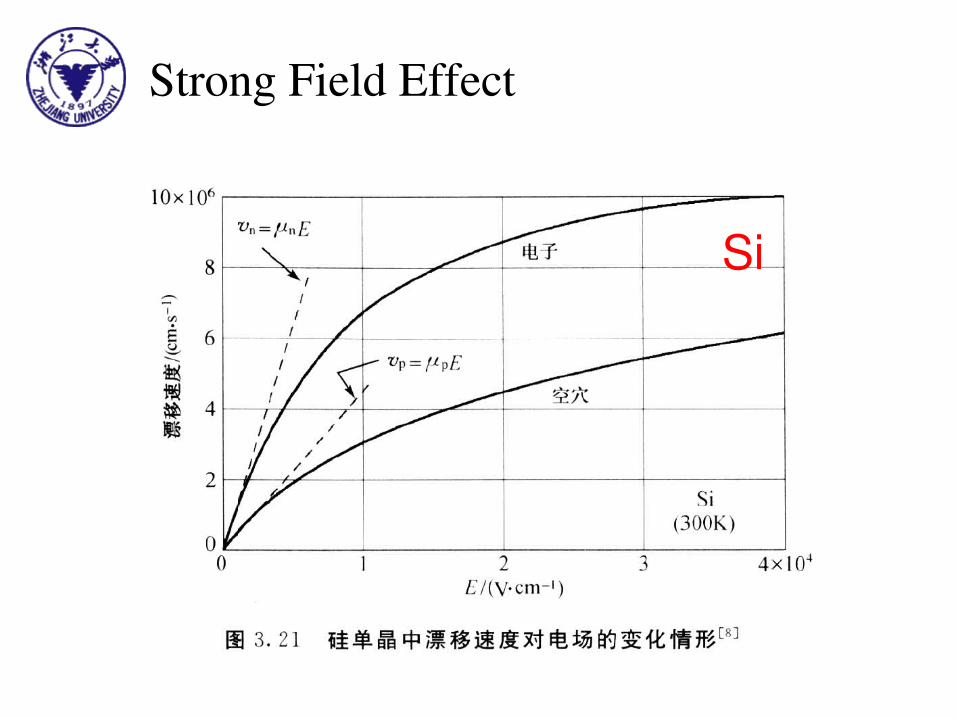
Strong Field Effect
Si
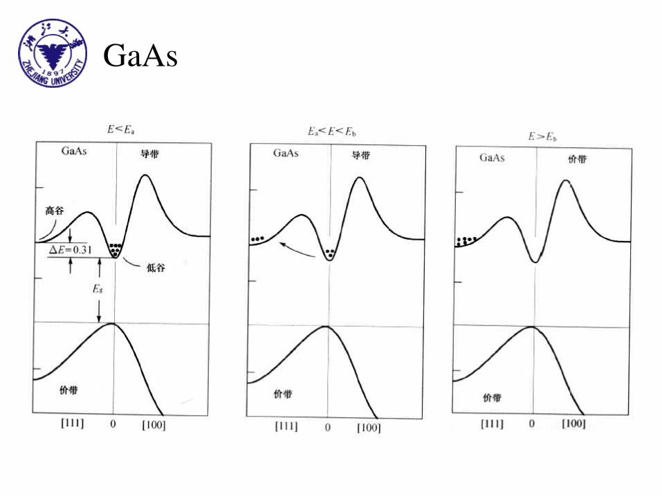
GaAs
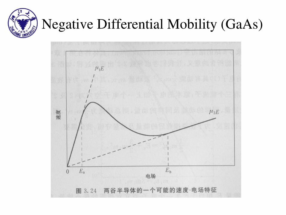
Negative Differential Mobility (GaAs)
Impact Ionization