Embed Size (px)
Citation preview

2012年 11月 12日 第14回窒化物半導体応用研究会 1
◆ はじめに
◆ 窒化ガリウム研究史
◆ GaN系LED, homo, DH, QW
◆ 白色LEDの現状と将来展望
GaN系白色LEDの現状
日亜化学工業株式会社 第二部門 開発本部
向井孝志

2012年 11月 12日 第14回窒化物半導体応用研究会 2
1879~
0.5 M years
1946~ 1996~

2012年 11月 12日 第14回窒化物半導体応用研究会 3

2012年 11月 12日 第14回窒化物半導体応用研究会 4
◆ はじめに
◆ 窒化ガリウム研究史
◆ GaN系LED, homo, DH, QW
◆ 白色LEDの現状と将来展望

2012年 11月 12日 第14回窒化物半導体応用研究会 5
1930s GaN研究始まり 1970頃 MIS構造 青色LED 商業ベース発表(RCA) 1980頃 MIS青色 フリップチップ型(Matsusita) GaN結晶性、p-GaNの壁 1983年 AlNバッファ層 , MBE(Yoshida) 1986年 AlNバッファ層 , MOCVD(Akasaki) GaN結晶性良くなる 1989年 p-GaN:Mg + 電子線処理(Amano) 低抵抗p-GaN第1歩
GaN研究史(Topics)

2012年 11月 12日 第14回窒化物半導体応用研究会 6
GaN開発史(日亜化学)と実用化
1989年 GaN開発開始 1991年 GaNバッファ層で良質のGaN膜 1992年 p-GaN Mgドープ+アニール H補償の提案 1992年 良質のInGaN 1993年 青色LED発表 1995年 LD室温パルス発振 1993年 1 mW 青色LED λp: 450(nm) ηext 2.2(%) 1994年 2 mW 青色LED λp: 450(nm) ηext 4.4(%) 1995年 3 mW 青色LED λp: 465(nm) ηext 5.6(%) 2 mW 緑色LED λp: 520(nm) ηext 4.2(%) 1996年 白色LED 視感効率 7.5(lm/W) 1999年 5 mW 青紫LD 2000年 30 mW青紫LD 2001年 紫外LD、青色LD (366~470nm)

2012年 11月 12日 第14回窒化物半導体応用研究会 7
基板の問題
・格子整合
・熱膨張係数
・耐熱性
・化学的安定性
サファイア、SiC、GaAs、Si GaN?
2012年 11月 12日 第14回窒化物半導体応用研究会 8
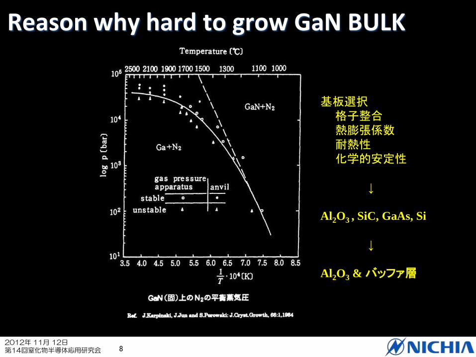
Reason why hard to grow GaN BULK
基板選択
格子整合
熱膨張係数
耐熱性
化学的安定性
↓
Al2O3 , SiC, GaAs, Si
↓
Al2O3 & バッファ層

2012年 11月 12日 第14回窒化物半導体応用研究会 9
Pioneers (MOCVD and Nitride growth)
Manasevit (1968) MOCVD
Maruska, Pankove, Akasaki Nitride Res. (around 1970)
Amano LT-buffer p-type
Nagatomo InGaN
Nishinaga, NEC Micro-Channel Epitaxy, ELO
Above and many other researches enabled practical GaN devices

2012年 11月 12日 第14回窒化物半導体応用研究会 10
低温成長GaN-Buffer層
低キャリア濃度 → p型GaN (アンドープ)
・表面平坦性の改善
・残留ドナー濃度の低減
・高移動度
効果

2012年 11月 12日 第14回窒化物半導体応用研究会 11
GaN成長の概略 - 成長プロファイル
基板クリーニング GaN成長
GaNバッファー層成長
510 ℃
1035 ℃
N源 NH3 Ga源 TMG キャリアガス H2
成長条件
・NH3 4 ℓ/min ・TMG 27 μmol/min, buf. 54 μmol/min ・サブフローガス H2 10 ℓ/min N2 10 ℓ/min ・メインフローキャリアガス H2 2 ℓ/min

2012年 11月 12日 第14回窒化物半導体応用研究会 12
GaNの伝導型制御
1. p型GaN(AlGaN)
ドーパント Mg、Zn、Cd、Be
問題点 As Depoで高抵抗(106 Ω㎝)
解決策 電子線照射(1989,Akasaki)
アニーリング(1992,Nakamura)

2012年 11月 12日 第14回窒化物半導体応用研究会 13
アニール処理
低抵抗p型GaN
MgとHの結合 → 高抵抗
アニール
Mg-Hの解離 → 低抵抗
2012年 11月 12日 第14回窒化物半導体応用研究会 14
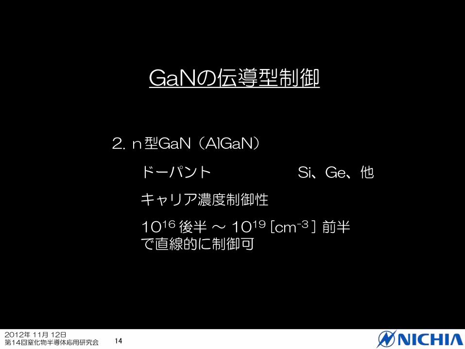
GaNの伝導型制御
2. n型GaN(AlGaN)
ドーパント Si、Ge、他
キャリア濃度制御性
1016 後半 ~ 1019 [cm-3 ] 前半 で直線的に制御可

2012年 11月 12日 第14回窒化物半導体応用研究会 15
◆ はじめに
◆ 窒化ガリウム研究史
◆ GaN系LED, homo, DH, QW
◆ 白色LEDの現状と将来展望

2012年 11月 12日 第14回窒化物半導体応用研究会 16
n-GaN/p-GaN HOMO-LED
・発光出力 <100(μW) ηext < 0.18(%)
・発光スペクトル: 450(nm) + 560(nm) (青白い発光)
要高出力化
1. HOMO-LEDの最適化
2. DH構造 → 活性層としてのInGaN
2012年 11月 12日 第14回窒化物半導体応用研究会 17
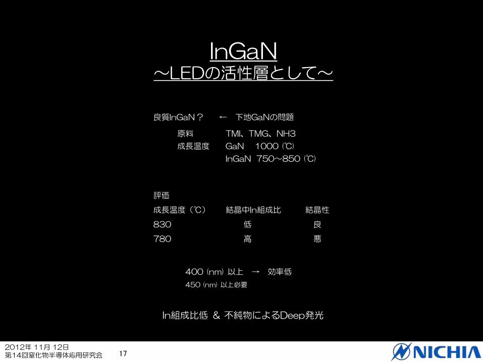
InGaN ~LEDの活性層として~
良質InGaN ? ← 下地GaNの問題
原料 TMI、TMG、NH3
成長温度 GaN 1000 (℃)
InGaN 750~850 (℃)
評価
成長温度(℃) 結晶中In組成比 結晶性
830 低 良
780 高 悪
400 (nm) 以上 → 効率低
450 (nm) 以上必要
In組成比低 & 不純物によるDeep発光
2012年 11月 12日 第14回窒化物半導体応用研究会 18
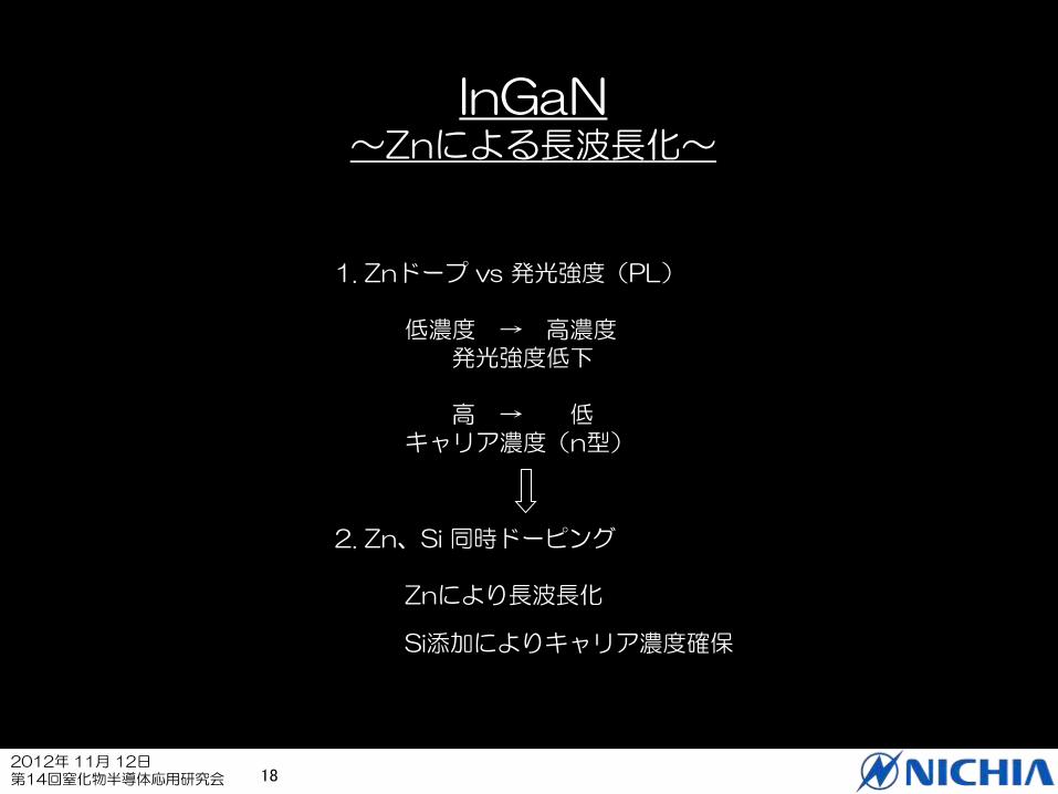
InGaN ~Znによる長波長化~
1. Znドープ vs 発光強度(PL)
低濃度 → 高濃度 発光強度低下
高 → 低 キャリア濃度(n型)
2. Zn、Si 同時ドーピング
Znにより長波長化
Si添加によりキャリア濃度確保

2012年 11月 12日 第14回窒化物半導体応用研究会 19
特性 DH-LED(InGaN:Zn+Si)
発光出力 2.4 (mW)
順方向電圧 3.6 (V)
ピーク波長 450 (nm)
スペクトル半値幅 70 (nm)
If = 20(mA) , Ta=25(℃)

2012年 11月 12日 第14回窒化物半導体応用研究会 20
量子井戸(QW)構造 InGaN・LED
1. コンセプト
・GaN/InGaN ミスフィットの問題
InGaN層を薄く → 格子歪み
(2.5~3 nm)ミスフィット転位防止
↓↓
高Inモル分率
(青色LEDの高性能化/緑色InGaN・LED)

2012年 11月 12日 第14回窒化物半導体応用研究会 21
量子井戸(QW)構造 InGaN・LED
2. 青、緑色 SQW・LED
・構造
InGaNの薄膜化 (その他同じ)
高Inモル分率
アンドープInGaN
・構造の確認
ガス切替
合金化 TEM、SIMSで確認
Si、Mgの拡散
2012年 11月 12日 第14回窒化物半導体応用研究会 22
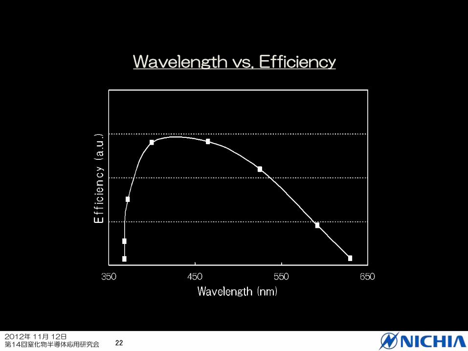
Wavelength vs. Efficiency
350 450 550 650
Wavelength (nm)
Effic
ien
cy (
a.u
.)

2012年 11月 12日 第14回窒化物半導体応用研究会 23
◆ はじめに
◆ 窒化ガリウム研究史
◆ GaN系LED, homo, DH, QW
◆ 白色LEDの現状と将来展望

2012年 11月 12日 第14回窒化物半導体応用研究会 24

2012年 11月 12日 第14回窒化物半導体応用研究会 25
Theoretical Limit of Luminous Efficiency Calculation from∫I(l)KmV(l)S(l)dl
I(l): Spectrum intensity of a white light source
KmV(l): Spectral luminous efficacy(683 lm/W @l=555nm)
S(l): Stokes Loss
∫I(l)dl=1W i.e. WPE of excitation source is 100%.
405nm-based White LED
203 lm/W Blue-based White LED(YAG)
263 lm/W
Tri-Phosphor FL
154 lm/W
Full LED system has the highest potential. Blue-based White LED is practically best way.
Full LED system
B:445nm, G:555nm, R:600 (line spectrum)
402 lm/W (Ra not considered)
Flat spectrum
180 lm/W
Other than YAG
(closed-door)
306 lm/W

2012年 11月 12日 第14回窒化物半導体応用研究会 26

2012年 11月 12日 第14回窒化物半導体応用研究会 27
Recent result in Nichia High Power White LED
Single chip type:
v: 203 lm
L: 183 lm/W
WPE: 48.3 %
at 350mA, 3.18 V
chromaticity coordinates (x, y)=(0.36, 0.39)
Tcp: 4700 K
Multi chip type:
v: 1913 lm
L: 135 lm/W
WPE: 37.1 %
at 1 A, 14.16 V (4-series)
chromaticity coordinates (x, y)=(0.35, 0.38)
Tcp: 4700 K

2012年 11月 12日 第14回窒化物半導体応用研究会 28
Energy conversion of white LED
0%
20%
40%
60%
80%
100%
100% Elec. input 64%
32%
4%
Blue light
Loss in chip
14%
36%
14%
Blue light
Yellow light
Loss in package
50% 160 lm/W
Heat emission
(to outside of chip) (to outside of package)
-nonradiative
-absorb
L=160lm/W, Tcp=5,600K, If=20mA, Vf=2.8V
-stokes loss
-absorb
50%
-series R
-contact R
White light

2012年 11月 12日 第14回窒化物半導体応用研究会 29
Light Extraction: Past Blue LED Structure
Absorption
60% of generated light
travels in nitride films.
Low η ext
Sapphire Substrate
Ni/Au Translucent
p-Electrode
Epi-Layer
Conventional Type
Reducing optical absorption at p-electrode is very important.
Low Transmittance & Large Optical Absorption
2012年 11月 12日 第14回窒化物半導体応用研究会 30
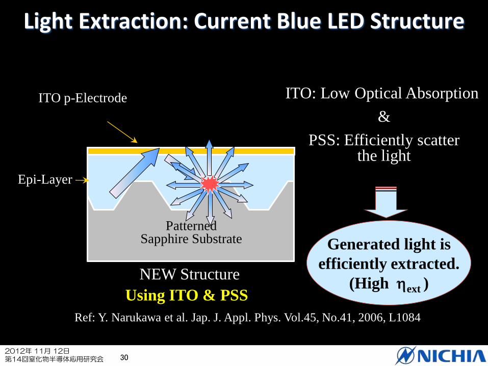
Light Extraction: Current Blue LED Structure
Patterned Sapphire Substrate
NEW Structure
Epi-Layer
ITO p-Electrode ITO: Low Optical Absorption
&
PSS: Efficiently scatter the light
Generated light is
efficiently extracted.
(High ext ) Using ITO & PSS
Ref: Y. Narukawa et al. Jap. J. Appl. Phys. Vol.45, No.41, 2006, L1084

2012年 11月 12日 第14回窒化物半導体応用研究会 31
Vf reduced Blue LED
0 10 20 302
2.5
3
3.5
2
2.5
3
3.5
Current (mA)
Vf(V
)
@DC
HE-Blue2
HE-Blue1
0 10 20 300
20
40
60
80
100
0
20
40
60
80
100
Current (mA)
ex (
%)
@DC
WP
E (
%)
①Optimizing Epi-wafer for lower Vf.
②Applying current spreading electrodes.
Vturn-on (V) Rs (W) Vf (V) fe (mW) ex (%) WPE (%)
unoptimized 2.72 16 3.08 42.2 75.5 68.6
optimized 2.65 7.4 2.81 39.7 71.0 70.6
int: slight drop
ext: slight drop
2.81V 2.65 V
2.72 V 16 W
7.4 W
Side effects
2012年 11月 12日 第14回窒化物半導体応用研究会 32

2012年 11月 12日 第14回窒化物半導体応用研究会 33

2012年 11月 12日 第14回窒化物半導体応用研究会 34
What should be improved?
・EQE drops with increasing current
carrier overflow(band structure)
auger recombination
carrier de-localization at high injection
(increase of defect’s negative affect)
,and so on
Reducing chip size can decrease total cost of LED

2012年 11月 12日 第14回窒化物半導体応用研究会 35
What should be improved?
・EQE drops at high junction temperature
common use of LED: junction temperature is 70-120
Accepting high temperature operation easy lamp designing

2012年 11月 12日 第14回窒化物半導体応用研究会 36
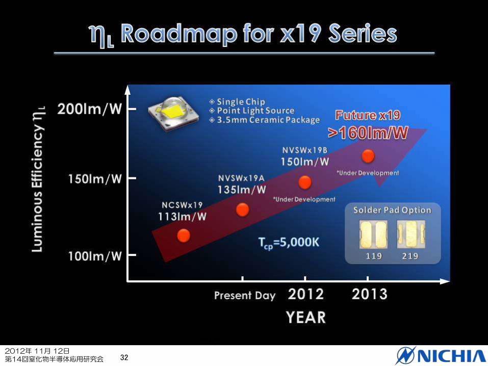
・White LEDs
249, 183, 135 lm/W Next target: 300, 200, 150 lm/W
at 20, 350, 1000 mA
・Green LEDs: Efficiency problem
・Deep UV LEDs: Efficiency, Voltage problem
まとめ、今後の課題
GaN-based LED
Truly required improvement for ultimate W-LEDs
・High efficiency at high current density
・High efficiency at high junction temperature
・Higher Phosphor’s color conversion efficiency
![TR28377D 사용자 매뉴얼 · 전력변환 실습회로 buck 컨버터 및 white led 부하 ... [그림 4-11] rgb led 설계 rgb led는 smd타 led 하나에 3가지 색상의 led가](https://img.pdfslide.tips/doc/110x75/5e4c6128cf06fe37c325954f/tr28377d-ee-ee-oeeoe-buck-e-e-white.jpg)


![BLACK&WHITE 140 LED OTTO [04.06.18] · Name - Nazwa - Naam - Name - Isim - название Nome - Nom - Numele - Meno - Jméno - Neve BLACK&WHITE 140 LED BLACK&WHITE 140 LED DE PL](https://img.pdfslide.tips/doc/110x75/5f481d0f3b482616b93518b5/blackwhite-140-led-otto-040618-name-nazwa-naam-name-isim-.jpg)