Embed Size (px)
Citation preview
PASJ: Publ. Astron. Soc. Japan , 1–??, 2005 February 25c© 2004. Astronomical Society of Japan.
Gigabit Digital Filter Bank: Digital Backend Subsystem in VERA DataAcquisition System
Satoru Iguchi,1 Tomoharu Kurayama,1,2 Noriyuki Kawaguchi,1 and Kazuyuki Kawakami31National Astronomical Observatory, 2–21–1 Osawa, Mitaka, Tokyo 181–8588
[email protected] of Astronomy, School of Science, The University of Tokyo, Hongo, Tokyo 113–0033
3Elecs Industry CO.,LTD, 1-22-23 Sinsaku, Takatu, Kawasaki 213–0014
(Received 2004 October 18; accepted 2004 December 25)
Abstract
The VERA terminal is a new data-acquisition system developed for the VERA project (VLBIExploration of Radio Astrometry), which is a project to construct a new Japanese VLBI (Very-Long-Baseline Interferometry) array dedicated to make a 3-D map of our Milky Way Galaxy in terms of high-precision astrometry. New technology; gigabit digital filter was introduced in the development. The impor-tance and advantages of digital filter for radio astronomy have been studied as follows: (1) the digital filtercan realize a variety of observation modes and keep the compatibility with the different data acquisitionsystems (Kiuchi et al. 1997 and Iguchi et al. 2000a), (2) the folding noise occurring in the samplingprocess can be reduced by combination with higher-order sampling technique (Iguchi & Kawaguchi 2002a),(3) and an ideal sharp cut off bandedge and a flat amplitude/phase responses are approached by using alarge number of taps available to use LSI of a large number of logic cells (Iguchi et al. 2000a).
We developed the custom FIR (Finite Impulse Response) filter chips and manufactured the GigabitDigital Filter Banks (GDFBs) as the digital backend subsystem in the VERA terminal. In this paper, thedesign and development of the GDFB are presented in detail, and the performances and demonstrationsof the developed GDFB are shown.
Key words: instrumentation: interferometers— reference systems— radio continuum: general—radio lines: general— techniques: high angular resolution
1. Introduction
In radio astronomical observations, two completely dif-ferent types of celestial objects are observed with a radiotelescope and a same receiver. One is continuum emissionover a wide range of frequencies resulting from blackbodyor synchrotron radiations, and another is line emissionsarising from molecular/atomic/ionic species. Sometimesthe line emission source emits signals in two widely sepa-rated frequency regions originated in a high speed rotat-ing gas around a massive core. For a continuum emissionsource, the full range of the receiver band is processedwith a limited frequency resolution but for the line emis-sion source the specific frequency region should be pro-cessed with much higher frequency resolution. For thelatter case an analog bandpass filter of fixed bandwidthon a fixed central frequency has been used so far. Thefrequency tuning of the spectral line emission inside thenarrow band filter has been made by changing a frequencyof a local oscillator in the receiver. Two or more numberof limited spectrum of arbitrary separated in frequencyare difficult to receive simultaneously with the analog fil-ter of no function for frequency agility. The receiver onradio interferometry is capable to receive a wide frequencyrange of typically more than 1 GHz. The digital filter ofprocessing speed of 1 Gbit (gigabit) per second or highergives a perfect solution for these radio astronomical obser-
vations, because some frequency bands can arbitrary becut with the digital filter.
The VERA is a project to construct a new JapaneseVLBI system dedicated to differential VLBI to measurethe position and proper motion of the Galactic maserswith 10 microarcsec level accuracy (e.g. Sasao 1996;Honma et al. 2000). The VERA’s radio telescopes havefully-steerable dual-beam system with which we can ob-serve two adjacent sources simultaneously by moving thesteerable receivers with the Stewart platform (Kawaguchiet al. 2000). By removing the atmospheric fluctuation ef-fectively based on the dual-beam observation, the VERAcan measure the position of Galactic maser relative toextra-galactic reference source with unprecedentedly highaccuracy (Kobayashi et al. 2002). For the realization ofsimultaneously observing both Galactic maser and extra-galactic source, the GDFBs were implemented as the dig-ital backend subsystem in the data acquisition systemnewly developed for the VERA, the VERA terminal.
This paper presents the first astronomical capabilityand performances of our developed GDFB. An outline ofthis paper is as follows: section 2 shows the requirementsand specifications of VERA digital backend subsystem,the GDFB; section 3 presents the design and developmentof the GDFB; section 4 shows the digital filtering perfor-mances and astronomical demonstrations of the GDFB;and finally section 5 provides the summary of this paper.

2 S.Iguchi et al. [Vol. ,
FIR Filter1-p 2-b
32-M CK
QuantizerInput Phase Selector
32
Digital Filter Unit #15
Beam 1
Beam 2
FIR Filter1-p 2-b
32-M CK
QuantizerInput Phase Selector
32
Digital Filter Unit #1
Beam 1
Beam 2
FIR Filter1-p 2-b
32-M CK
QuantizerInput Phase Selector
32
Digital Filter Unit #0
Beam 1
Beam 232-p 2-b
32-M CK
sixteen Digital Filter UnitsInput I/F Unit Output I/F Unit
32
32-M,
16-M or 8-M CK
From ADC
32-p 2-b
32-M CK
Beam 1
Beam 2
To VERA
Recoding
system
8 To VSOP
Recoder
8 To RVC
VSOP/K-4 Interface Board
VSI-H Interface Board
1:4
1:2
1:2
16-p 2-b
32-M CK
8
8
8
4 8
32
32
32
32-M or
16-M CK
32-M or
16-M CK
Monitor & Control Unit
To PCD
SW
Matrix
SW
Matrix
To DSD
DSD Interface Board
16
32-M,
16-M or 8-M CK
MSB
LSB
16 32
Control Computer IRIG-B, I PPS, 32 MHz IRIG-B, 1 PPS, 32 MHz, UTC time code, Start sig.
Start sig.
Start sig.
1 PPS
VSI time code
TVG
1 pps
Fig. 1. Block diagram of Gigabit Digital Filter Bank (GDFB). The GDFB consists of Input I/F Unit, sixteen Digital FilterUnits, Output I/F Unit, and Monitor & Control Unit. The Input I/F Unit converts ECL (Emitter Coupled Logic) to TTL(Transistor-Transistor Logic), and measures the bit distribution of input signal from each ADC. The sixteen Digital Filter Unitsselect the input signals from each beam, and cut the requested bandwidth in frequency range of 512 MHz. Since the decimationfactor at the Digital Filter Units is fix 32, its output is 1-parallel 2-bit 32-MHz clock. Each Digital Filter Unit has the function ofbit distribution measurement for output signals after digital filtering. The GDFB supports the VLBI Hardware Standard Interface(VSI-H; see http://web.haystack.edu/vsi/index.html), and can directly connect the VSI-H Data Input Module in hardware interface.The Output I/F Unit is connected to the VERA recording system conformable to the VSI-H, the VSOP recorder to join the VSOPobservation (Iguchi et al. 2000a) and for K-4 recording (Kiuchi et al. 1997), and the Realtime VLBI Correlator (RVC, Iguchi etal. 2000b) and the Digital Spectral Detector (DSD) modifying for the VERA (from digital spectrometer developed in Sorai et al.2000) to check at realtime the digital spectrum of observation data that is directly recorded at the VERA recorder. The circle of1 PPS and Data streams from the VSI-H interface board means the transmission on the same cable. The Test Vector Generator(TVG) data streams are defined by the VSI-H, and this TVG is effective to check internal self-contained diagnostics and bit error,and confirm external interface connectivity to the recorders. The 8-MHz bandwidth is realized by choosing one sample every twoones in the Output I/F Unit. The Phase Calibration Detector (PCD), which is also made by improving the input board of DSD,is used to calibrate the relative phase fluctuation of different transmission path between Beam 1 and 2. The Monitor & ControlUnit sets up the parameters corresponding to each unit by the observation mode, synchronizes the data with the time, and monitorthe setting parameters and the status. The VSI time code (VERA specific) is generated in the VSI-H interface board from IRIG-Bsignal, 1 PPS and 32-MHz clock. Since an internal clock generator is introduced in the Monitor & Control Unit, it is also possibleto control the time even if it does not receive the IRIG-B signal, 1 PPS and 32-MHz clock.
2. Principles of Gigabit Digital Filter Bank(GDFB) Design
Two 2-bit Analog-to-Digital Converters (ADCs) work-ing at an 1-GHz sampling rate have been introduced fordual-beam system in a VERA radio telescope. The ADCswere fabricated by improving a digital oscilloscope madeby Sony/Tektronix Company (as developed in the BEARSproject: Sunada et al. 2000). However, the digital oscil-loscope was discontinued at present. The ADS-1000 madeby Digital Link Company will replace it as the next gener-ation VERA ADC at an early date. In the other data ac-quisition systems, the current standard bandwidth is 8 or16 MHz in astronomically observing, while the maximumnumber of IF is 16 channels (Iguchi et al. 2000a; Kiuchiet al. 1997; Napier et al. 1994; Whitney 1993). The
bandwidth compatibility with the other data acquisitionsystems is of significance in realizing global VLBI obser-vations. Thus, the VERA terminal has the requirementthat the GDFB can cut a 8-MHz bandwidth out of therange of 512 MHz.
For radio interferometry, the use of digital rather thananalog instrumentation to introduce the compensatingtime delays and to measure correlation has importantpractical advantages. For continuum emission sources onebit per sample or two bits per sample is simple to imple-ment and almost optimum in the sense that the Signal-to-Noise Ratio (SNR) is maximized for a limited trans-mission rate of the IF signals in connected radio inter-ferometry and a fixed number of bits recorded in VLBI(Thompson et al. 2001).
The VERA terminal has the digital processing which
No. ] Gigabit Digital Filter Banks in the VERA terminal 3
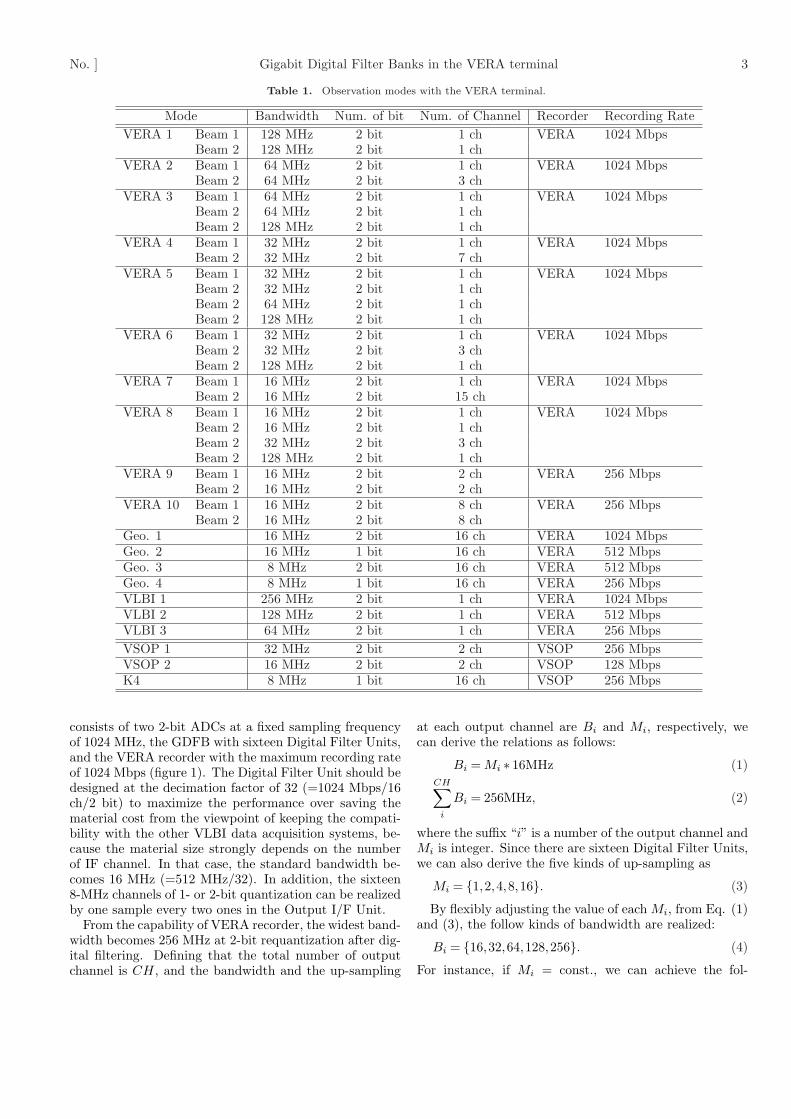
Table 1. Observation modes with the VERA terminal.
Mode Bandwidth Num. of bit Num. of Channel Recorder Recording RateVERA 1 Beam 1 128 MHz 2 bit 1 ch VERA 1024 Mbps
Beam 2 128 MHz 2 bit 1 chVERA 2 Beam 1 64 MHz 2 bit 1 ch VERA 1024 Mbps
Beam 2 64 MHz 2 bit 3 chVERA 3 Beam 1 64 MHz 2 bit 1 ch VERA 1024 Mbps
Beam 2 64 MHz 2 bit 1 chBeam 2 128 MHz 2 bit 1 ch
VERA 4 Beam 1 32 MHz 2 bit 1 ch VERA 1024 MbpsBeam 2 32 MHz 2 bit 7 ch
VERA 5 Beam 1 32 MHz 2 bit 1 ch VERA 1024 MbpsBeam 2 32 MHz 2 bit 1 chBeam 2 64 MHz 2 bit 1 chBeam 2 128 MHz 2 bit 1 ch
VERA 6 Beam 1 32 MHz 2 bit 1 ch VERA 1024 MbpsBeam 2 32 MHz 2 bit 3 chBeam 2 128 MHz 2 bit 1 ch
VERA 7 Beam 1 16 MHz 2 bit 1 ch VERA 1024 MbpsBeam 2 16 MHz 2 bit 15 ch
VERA 8 Beam 1 16 MHz 2 bit 1 ch VERA 1024 MbpsBeam 2 16 MHz 2 bit 1 chBeam 2 32 MHz 2 bit 3 chBeam 2 128 MHz 2 bit 1 ch
VERA 9 Beam 1 16 MHz 2 bit 2 ch VERA 256 MbpsBeam 2 16 MHz 2 bit 2 ch
VERA 10 Beam 1 16 MHz 2 bit 8 ch VERA 256 MbpsBeam 2 16 MHz 2 bit 8 ch
Geo. 1 16 MHz 2 bit 16 ch VERA 1024 MbpsGeo. 2 16 MHz 1 bit 16 ch VERA 512 MbpsGeo. 3 8 MHz 2 bit 16 ch VERA 512 MbpsGeo. 4 8 MHz 1 bit 16 ch VERA 256 MbpsVLBI 1 256 MHz 2 bit 1 ch VERA 1024 MbpsVLBI 2 128 MHz 2 bit 1 ch VERA 512 MbpsVLBI 3 64 MHz 2 bit 1 ch VERA 256 MbpsVSOP 1 32 MHz 2 bit 2 ch VSOP 256 MbpsVSOP 2 16 MHz 2 bit 2 ch VSOP 128 MbpsK4 8 MHz 1 bit 16 ch VSOP 256 Mbps
consists of two 2-bit ADCs at a fixed sampling frequencyof 1024 MHz, the GDFB with sixteen Digital Filter Units,and the VERA recorder with the maximum recording rateof 1024 Mbps (figure 1). The Digital Filter Unit should bedesigned at the decimation factor of 32 (=1024 Mbps/16ch/2 bit) to maximize the performance over saving thematerial cost from the viewpoint of keeping the compati-bility with the other VLBI data acquisition systems, be-cause the material size strongly depends on the numberof IF channel. In that case, the standard bandwidth be-comes 16 MHz (=512 MHz/32). In addition, the sixteen8-MHz channels of 1- or 2-bit quantization can be realizedby one sample every two ones in the Output I/F Unit.
From the capability of VERA recorder, the widest band-width becomes 256 MHz at 2-bit requantization after dig-ital filtering. Defining that the total number of outputchannel is CH, and the bandwidth and the up-sampling
at each output channel are Bi and Mi, respectively, wecan derive the relations as follows:
Bi = Mi ∗ 16MHz (1)CH∑
i
Bi = 256MHz, (2)
where the suffix “i” is a number of the output channel andMi is integer. Since there are sixteen Digital Filter Units,we can also derive the five kinds of up-sampling as
Mi = {1,2,4,8,16}. (3)
By flexibly adjusting the value of each Mi, from Eq. (1)and (3), the follow kinds of bandwidth are realized:
Bi = {16,32,64,128,256}. (4)
For instance, if Mi = const., we can achieve the fol-

4 S.Iguchi et al. [Vol. ,
Table 2. The relationship between the input phase (ΦI),the output phase (ΦO), and the output bandwidth (Bi) atthe observation mode of VERA 5.
Input Phase Digital Filter UnitsSelector
Unit Selection Input Output OutputNum. Beam Phase Bandwidth Phase
ΦI Bi ΦO
1 Beam 1 0 32 MHz 02 16 13 Beam 2 0 32 MHz 04 16 15 Beam 2 0 64 MHz 06 8 17 16 28 24 39 Beam 2 0 128 MHz 010 4 111 8 212 12 313 16 414 20 515 24 616 28 7
low observation modes: sixteen 16-MHz channels of 2-bitquantization, eight 32-MHz channels of 2-bit quantization,four 64-MHz channels of 2-bit quantization, two 128-MHzchannels of 2-bit quantization, and one 256-MHz chan-nels of 2-bit quantization. All observation modes with theVERA terminal are listed in table 1. The recording rate isalways reduced in case of the 8-MHz bandwidth or the 1-bit quantization which are effective for global geometricalobservation.
All observation modes can be realized by well control-ling the tap coefficients of FIR filter and the sample phaseshift of Input Phase Selector that have a role of keepingthe consistency between the sixteen Digital Filter Units(see figure 1). Defined that the input phase in the InputPhase Selector is ΦI , the output phase after digital filter-ing is written as
ΦO =ΦI
32∗ Bi(MHz)
16(MHz), (5)
where 32 is the decimation factor in the sixteen DigitalFilter Units, and then its minimum bandwidth is 16 MHz.The various bandwidths can be realized by well adjust-ing the input phase under the condition that the out-put phases from the corresponding Digital Filter Unitsare continuously time-series (0,1,...). For example, in caseof the observation mode of VERA 5, the relationship be-tween the input phase, the output phase and the outputbandwidth is shown in table 2. It is understood that theInput Phase Selector does not only select the signals fromeach beam but also realize more than 16-MHz bandwidthby well adjusting the input phase.
The other data acquisition systems have several IF
Bandpass Filtering
B/2
-Bc
-B/2
Bc
0
H(f)
0
Folding
Noise
After filtering
f
f
f0
f0
/2 /20
0
Fig. 2. Frequency response H(f) of digital filter. It is obvi-ous that the effect of the aliasing, the folding noise, decreasesas the cut-off frequency (Bc) of filter becomes narrower thanthe bandwidth (B), whereas it increases as the cut-off fre-quency is higher than the bandedge. It is well known thatthe non-rectangular response provides an increase in the sta-tistical independence between samples.
down converters (Kiuchi et al. 1997; Napier et al.1994; Whitney 1993), so that can tune the IF frequencyindependently for every IFs, and also select Upper- orLower-sidebands. However, the GDFB do not have tun-able digital filter function. When the VERA participatesin a global VLBI observation, the other VLBI networksneed to adapt the IF frequency and sideband selection torespond to a VERA observation mode.
3. Detailed Design and Development of GDFB
By limiting the tap length in the FIR filter, it is im-possible to realize a filter with the perfectly rectangularbandpass response (figure 2). The FIR filtering system iswritten as
t(n) =K−1∑
i=0
h(i) ∗ s(n− i), (6)
where s is the digital waveforms from the astronomicalradio signals and obeys the zero-mean Gaussian randomvariable, t is the output signals from FIR filter, and h arethe FIR filter function with the tap length of K. Thematerial size of FIR filter directly depends on the taplength and the tap-coefficient word length. In developingthe FIR filter, it is important to define these parameters.In subsection 3.1 these estimations are derived, the logicof FIR filter is described in subsection 3.2, subsection 3.3presents the custom FIR filter chip and the Digital FilterUnit board, and finally subsection 3.4 shows the GDFB.

No. ] Gigabit Digital Filter Banks in the VERA terminal 5
0 1024 2048 3072 4096
1.000
0.975
0.950
0.925
0.900
0.875
0.850
Num. of Tap
Sen
siti
vit
y L
oss
Fac
tor
Fig. 3. The relationship between the tap length and thesensitivity loss factor. The results are obtained from the FIRfilter in which Bc is equal to B and the Hanning windowfunction is used.
3.1. The tap length and the tap-coefficient word length
It was confirmed that the folding noise is decreased bythe phase-rotation stopping technique in VLBI correlationprocess designed to correct a different Doppler shift infrequency at two antennas by the earth rotation (Iguchiet al. 2000a). By considering the correlation process inradio interferometry, the sensitivity loss factor due to theimperfect bandpass is derived as [see Eq. (2) in Iguchi &Kawaguchi 2002a],
ξ =
∫ f0+B/2
f0−B/2
Hx(f)H∗y (f)df
B
× 1√
¥¥1+ 2
N−1∑τ=1
N − τ
N
Rxx(τ)Ryy(τ)Rxx(0)Ryy(0)
, (7)
where B is the bandwidth after filtering, N is the numberof samples existing in the integration period, Hx(f) andHy(f) are the frequency response of bandpass filter, andRxx and Ryy are the autocorrelation functions of x and y,those are the output signals of two telescopes. The digitalfilter technique can realize the stable bandpass frequencyresponses, so that the relation Hx(f) = Hy(f) = H(f) isderived. The signal that is received through each tele-scope is written as the follow relations; x(n) = Cx · t(n)and y(n) = Cy · t(n) where C is the constant factor esti-mated from effective sensitivity at each telescope. WhenCx = Cy, Eq. (7) is simply replaced as
ξ =
∫ f0+B/2
f0−B/2
|H(f)|2df
B
√¥¥1+ 2
N−1∑τ=1
N − τ
N
R2tt(τ)
R2tt(0)
. (8)
For instance, the FIR filter function with bandpass re-sponse is generally written as
10 15 20 25 30
1.00
0.99
0.98
0.97
0.96
0.95
0.94
Num. of bit
Sen
siti
vit
y L
oss
Fac
tor
0.93
Fig. 4. The relationship between the tap-coefficient wordlength and the sensitivity loss factor. The results are obtainedfrom the FIR filter with the tap length of 1024.
Table 3. The specifications of Digital Filter Unit.
Minmum Bandwidth 8 MHz in 512 MHzNum. of tap 1024Tap-coefficient word length 13 – 14 bitsPerformance at 8 MHz in 512 MHzSensitivity loss factor in SNR 0.97Loss 3 %
h(i)=w(i)·2cos[2π(i−L)
f0
B
]· Bc
2B
sin[(i−L) Bc
2B π]
(i−L) Bc
2B π,(9)
where Bc is the cut-off frequency of filter, L is the groupdelay, and w is the window function to save the Gibb’sphenomenon. Under the requirement that the digital filtercuts a 8-MHz bandwidth out of the range of 512 MHz,from Eq. (6), (8) and (9) by generating the Gaussianrandom variable, we can derive the relationship betweenthe tap length and the sensitivity loss factor as shown infigure 3. We decide the tap length of 1024 for the VERAterminal by comparison between the material size and thesensitivity loss factor. Then, using the same method, wecan show the relationship between the tap-coefficient wordlength and the sensitivity loss factor as shown in figure 4.Finally, we decided the tap-coefficient word length of 13– 14 bits to realize the minimum material size and cost inthe sense that sensitivity loss factor is about 0.97 (=3 %loss). The specifications of Digital Filter Units are listedin table 3.
3.2. The logic of FIR filter
From the decimation factor of 32 in the Digital FilterUnit, Eq. (6) is written as
t(n) =31∑
k=0
K/32−1∑
j=0
h(32j + k) ∗ s[n− (32j + k)], (10)
where i = 32j + k. According to an arbitrary k(=c), thesummation of Eq. (10) is replaced as
∑h(32j + c) ∗ s[n− (32j + c)] =
∑h(l) ∗ s(n− l),(11)

6 S.Iguchi et al. [Vol. ,
20-b
2-b
2-b
1-p 25-b
32-M CK
SFFU #0
SFFU #1
SFFU #30
SFFU #31
2-b
2-b
20-b
20-b
20-b
32-p 2-b
32-M CK Σ
Odd Mode
Set
Tap coeff.
Selector
Fig. 5. Block diagram of 32-parallel processing of a FIR fil-ter. The input signals are 32-p 2-bit 32-M CLK, while theoutput signals are 1-p 25-bit 32-M CLK. The beam selectionis done at the last stage, the Input Phase Selector, and the re-quantization to 2 bits is done at the next stage, the Quantizer(see figure 1). The selector and a switch can change over be-tween odd tap length or ever one. The SFFU is shown infigure 6.
2-b
Odd Mode
Set
Tap coeff.
Z-1
Z-1
+3-b
h
2-b
Z-1
Z-1
+3-b
h
0
Z-1
Z-1
+3-b
h
Σ
16-b 16-b 16-b
20-b
2-b
2-b
16 stages
Fig. 6. Block diagram of Symmetric FIR Filter Unit(SFFU). One SFFU is 32-tap FIR filter, and has 7-levellook-up table represented by 16-bit word length as multiply-ing the tap-coefficient word length by the result after addingthe signal and returned one. The output bit length becomes20 bits [16 bit + log2 (16 stages)]. The switch changes overbetween odd tap length or ever one.
where 32j+c= l, and shows the same equation as Eq. (6),although its tap length becomes K/32. These imply thatthe 1024-tap FIR filter consists of 32-parallel independentdigital filter with tap coefficients corresponding to eachother of h(32j + c). In Eq. (6), t(n) is calculated froms(n) to s(n−K +1) with the K continuous samples, andis expressed as follows.
t(n) <= s(n) ,s(n− 1), · · · ,s(n−K + 1)t(n +1) <= s(n +1),s(n) , · · · ,s(n−K + 2)t(n +2) <= s(n +2),s(n +1), · · · ,s(n−K + 3)
: :
However, since the down sampling of 1/32 is realized bychoosing t(n) every 32 samples, the data from t(n+1) tot(n + 31) are negligible or thrown out. Thus, Eq. (10) isrewritten as
Fig. 7. Photograph of the custom FIR filter chip.
t(32m) =31∑
k=0
K/32−1∑
j=0
h(32j +k)∗s[32m− (32j +k)],(12)
where n = 32m.The FIR filter function with the even symmetrical re-
sponse, in case that the number of tap is even, has thefollow relation as
h(K − 1− i) = h(i). (13)
Then, Eq. (12) of a FIR filter is replaced as
t(32m) =31∑
k=0
K/64−1∑
j=0
h(32j + k) ∗ [s(32m− 32j− k)
+s(32m−K +32j + k + 1)]. (14)
The block diagram with such an algorithm is shown in fig-ure 5. First summation composes the 32-parallel process-ing, and second summation does the Symmetric FIR FilterUnit (SFFU) as shown in figure 6. The 16-bit word lengthaftter multiplying enables us to understand that the tap-coefficient word length of more than 13 bits is achievedin this design, because 3-bit outputs from adders aftershifting are not represented by 8 levels but not 7 ones.
3.3. The custom FIR filter chip and the Digital FilterUnit board
The Digital Filter Unit with 1024 taps consists offour the custom FIR filter chip that was made of“Application Specific Integrated Circuit (ASIC)” (see fig-ure 7). The custom FIR filter chip is the SLA50000H se-ries (SLA550QH) with the LSI package of QFP8-208 pin,0.35 µm silicon gate CMOS using 4-layer Al interconnectprocess made of the Seiko Epson Corporation. The op-erating voltage is 3.3±0.3 V at I/O, and 2.0 ±0.2 V atinternal logic, while the operating ambient temperature is0 to 70 ◦C at wind speed of 0 m/s. The eight SFFUs (seefigure 6) are packed into a custom FIR filter chip that hasa capability of 256 taps. Then, the output bit length fromthe FIR filter chip becomes 23 bits [20 bit + log2 (8)].In addition, the function of the bit distribution measure-ment is implemented in the FIR filter chip to maximize

No. ] Gigabit Digital Filter Banks in the VERA terminal 7
Fig. 8. Photograph of the Digital Filter Unit board. Thesize is (W) 310 mm × (D) 233.33 mm.
the performance of digital filtering. The electric powerconsumption is 420 mW at 3.3 (V), and 620 mW at 2.0(V).
As shown in figure 8, the Digital Filter Unit boardconsists of two Digital Filter Units; eight custom FIRfilter chips, three Field Programmable Gate Arrays(FPGA) which are ACEX series 1K30 made of ALTERACorporation, and 3.3V onboard power supply. The meritof this structure is that the board size is minimized by be-ing able to implement each quantization function in oneFPGA. The Input Phase Selector is made of one FPGA,the 1024-tap FIR Filter is made of four custom FIR filterchips, and two Quantizers are included in last one FPGA.A single-phase DC-DC power module is the RM100-48-3.3 made of Densei-Lambda K.K., and converts 48 V to3.3 V with the maximum output power of 66 W at 86 %efficiency. The nominal output power is 38.8 W, that iscorresponding to 59 % load.
3.4. The GDFB
The GDFB module board placement is shown in fig-ure 9. The filter module consists of one Monitor &Control Unit board, one Input I/F Unit board, one datathroughout board, two Power Supply boards, eight DigitalFilter Unit boards, and one filter output board. The out-put module consists of one filter input board, one VSI-H interface board, one VSOP/K-4 interface board, oneDSD interface board, one Power Supply board, 16 con-trol keys, and the monitor and control panel, which hasstatus alarms, a reset switch, a time display LED (Light-Emitting Diode), and a LCD (Liquid Crystal Display) tomonitor and control.
The connector specifications of input/output are MDR-68 pin (ECL level), MDR-80 pin and MDR-14 pin [LVDS(Low Voltage Differential Signaling) level], DSUB-25 pin(ECL level), DHA-50 pin (ECL level), FC-10 pin (RS485level), BNC (ECL level), and BNC (TTL level). FourMDR-68 pin connectors receive data streams from twoADCs, and others transmit them to the PCD. One MDR-
Table 4. The specifications of Gigabit Digital Filter Bank.
Configuration: Filter Module,Output Moduleand Power Module
Filter Module: 16 Digital Filter Unitswith 1024 tap lengths
Input Data Rate:ADC: 2048 Mbps × 2 beams
Observation modes:see Table 1
Output Data Rate:VERA Recorder: 1024, 512, 256 MbpsVSOP Recorder: 256, 128 MbpsRVC: 256, 128 MbpsDig. Spectro.: 1024, 512, 256 MbpsPCD: 2048 Mbps × 2 beams
Monitor & Control:Control Computer controlsvia GPIB IEEE-488
Dimensions: (W) (H) (D)Filter Module: 49 x 50 x 50 cmOutput Module: 49 x 50 x 50 cmPower Module: 49 x 10 x 50 cm
Total: 49 x 110 x 50 cmWeight:Filter Module: 28.0 kgOutput Module: 22.2 kgPower Module: 13.2 kg
Total: 63.4 kgPower Consumption:Filter Module: 610 WOutput Module: 140 W
Total: 750 W
14 pin connector receives the IRIG-B signal, 1 PPS and32-MHz clock, and another MDR-14 pin connector trans-mits the VSI time code to VERA recording system. TheECL-level BNC connector transmits Start sig. to theRVC, and the TTL-level BNC connectors transmit 1 PPSto the VSOP recorder and Start Sig. to the DSD. TheMDR-80 pin connector transmits the VSI-H specificationdata streams to the VERA recording system, the DSUB-25 pin connector transmits the VSOP/K4 data streamsto the VSOP recorder and the RVC, and the DHA-50 pinconnector transmits the DSD data streams to the DSD.
The power consumption of the filter module is 610 W,while that of the output module is 140 W. Total AC poweris 750 W at1-phase 100 VAC 50/60 Hz. Total weight ofthe GDFB is 63.4 kg.
The summary of GFDB key specifications is listed inTable 4.
4. Performance and demonstration
This section shows the evaluation results of the VERAdigital backend subsystem, the GDFB, in the VERA ter-minal. We present the simulation results to estimate the

8 S.Iguchi et al. [Vol. ,
(c)
(b)
(f)
(e)
(g)
(i)
(h)
(j)
MDR-68 pin
MDR-68 pin
DHA-50 pinDC connector
DSUB-25 pin
MDR-80 pin
MDR-14 pin
BNC
(a)
(d)
MDR-68 pin
GPIB
IEEE 488
RS232
FC-10 pin
Fig. 9. The GDFB board placement. There are two modules; one is the filter module (top: left is front view, and right is backview) at the size of (W) 490 mm × (H) 500mm × (D) 500 mm, and another is the output module (bottom: left is front view, andright is back view) at the size of (W) 490 mm × (H) 500mm × (D) 500 mm. By referring figure 1, (a) is the Monitor & ControlUnit board, (b) is the Input I/F Unit board, (c) is the data throughout board for the PCD, (d) is the Power Supply board, (e)is the Digital Filter Unit board, (f) is the filter output board from sixteen Digital Filter Units, (g) is the filter input board fromthe filter module, (h) is the VSI-H interface board, (i) is the VSOP/K-4 interface board, and (j) is the DSD interface board. Thedistribution of input signals to sixteen Digital Filter Units is done in the back-panel. The Output I/F Unit is implemented in theoutput module, and consists of (g), (h), (i), and (j). The total size of the GDFB is (W) 490 mm × (H) 1100mm × (D) 500 mm,including the power supply module.
digital loss factor including the requantization process af-ter digital filtering (see subsection 4.1) and the measure-ment results of the VERA GDFB frequency response todeeply investigate the stopband and sharpness of digitalfilter after requantizing (see subsection 4.2), demonstratethe VERA observations with GDFBs to verify the astro-nomical GDFB response (see subsection 4.3), and discussabout the bandedge and folding noise of digital filter (seesubsection 4.4).
4.1. Digital loss factor
The astronomical analog waveforms are sampled byADCs with 4-level (2-bit) quantization in the VERA sys-tem. The GDFB cuts the requested frequency bands inthe digital waveforms with 4-level quantized sampling.The digital waveform after digital filtering is representedwith multi-level quantized sampling in the calculation pro-
cess of digital filter as shown in Eq.(6). Then, it re-quires the requantization after digital filtering, becausethe recording data rate, the digital data transmission rateor the data processing rate is limited by the instrumentalcapability. The quantization noise in digitizing is inves-tigated on a theoretical basis (Thompson et al. 2001;Iguchi & Kawaguchi 2002a). It is well known that thedigital loss factor becomes 0.64 at 2-level (1-bit) quan-tization loss factor and 0.88 at the 4-level quantizationloss factor. However, the digital noise effect by requan-tization process had been unknown in cases of the inputand output waveforms with 2- or 4-level quantized sam-pling. In this paper, the computer simulation was run toinvestigate the digital loss factor including the requanti-zation process after digital filtering the digital waveformswith 4-level quantized sampling. In this simulation, the1/4-bandpass digital filter with 1024 taps was used to di-

No. ] Gigabit Digital Filter Banks in the VERA terminal 9
Table 5. The simulation results of digital loss factor includ-ing the requantization process after digital filtering the digitalwaveforms with 4-level quantized sampling, excluding the fre-quency response of digital filter.
Digital loss factorQuantization Requantization Theory Simulation
2 levels – 0.64 0.64±0.014 levels – 0.88 0.88±0.014 levels 2 levels 0.59±0.014 levels 4 levels 0.81±0.01
minish the effect of digital filter bandpass response. Thisis much more than those of the GDFB, 1/64-bandpass dig-ital filter (=8 MHz/512 MHz) with 1024 taps (see Table3), and then corresponds to the 8192 taps in the GDFB.
The SNR on correlation with unquantized samplingcan be written as simple
SNR =Rxy(0)√
Rxx(0)Ryy(0)+ R2xy(0)
√N
=ρ√
1+ ρ2
√N, (15)
where Rxy is the cross-correlation function between x andy, Rxx and Ryy are the autocorrelation functions of x andy, respectively, ρ is the correlation coefficient and “N isthe number of samples with the Nyquist rate. To esti-mate the loss within 1% of the true value, SNR is neededto be more than 100. In this simulations, the correlationcoefficient of 0.109 (=0.352/
√(12 + 0.352)2) when com-
mon/independence component in x and y is 0.35, and Nof 1048576 are used to achieve SNR of 111 from the fol-lowing two conditions. (1) The most correlation coeffi-cient will be less than 0.1 for the very small flux densitiesof cosmic radio sources. (2) Since the astronomical signalwaveforms obeys the zero-mean Gaussian random vari-able, it is difficult to provide long-series Gaussian noisedata points.
The simulation results are listed in Table 5. Fromcomparison of the theoretical estimations with the sim-ulation results in 2-level and 4-level quantizations, it isconfirmed that the simulation measurement with 1 % pre-cision can be achieved. If the requantization process hada linear response, the digital loss factor would be 0.56(=0.881*0.637) and 0.78 (=0.881*0.881) at 2-level and4-level requantizations after digital filtering the digitalwaveforms with 4-level quantized sampling, respectively.However, the simulation results show the digital loss fac-tors of 0.59 and 0.81 (see table 5). This means that therequantization process of the input and output waveformswith 2- or 4-level quantized sampling has a nonlinear re-sponse. The least significant bit (LSB) has 50 % uncer-tainty, and then these rounding errors are accumulatedin the calculation process of digital filtering as shown inEq.(6). Although multi-level digital waveforms seem to beapproximately equal to the analog waveforms, those digi-tal waveforms has the rounding errors accumulated by the
input digital waveforms with the digital loss factor of 0.88.On the other hand, the 2- or 4-level requantization will cutoff not only the information of signal component but also apart of the effects of rounding errors and quantization loss.Actually, the digital loss factor of 0.81 agrees completelywith that of 3-level (2-bit) quantization (see Thompson etal. 2001). The simulation results show that the digitalloss factor is not 0.56 but 0.59 and not 0.78 but 0.81 in 2-level and 4-level requantizations after digital filtering thedigital waveforms with 4-level quantized sampling.
4.2. VERA GDFB frequency response
Figure 10 shows a block diagram of the measurementsetup of the GDFB frequency response. To investigatethe frequency response, it is useful to use the CW sig-nal which can measure the folding effects by sweeping thefrequency range of 0 to 512 MHz. The white noise is im-portant to measure the frequency response, because theastronomical signals obey the Gaussian random variable.To approximate the zero-mean Gaussian probability, theinput signals are a combination of both the CW signaland the white noise.
The frequency response before digital filtering is donewith the PCD, and is written as
P Ion(f) =
[|C(f)|2 + |N(f)|2] ·H1(f)H∗2 (f), (16)
where C(f) is the frequency response of CW signal, N(f)is the frequency response of the white noise from theVERA analog backend subsystem, and H1 and H2 are thefrequency response by the different transmission path, inwhich H1 =Ht1Ha1 and H2 =Ht2Ha2 (see figure 10). Thebandpass calibration is essential for estimation of the pre-cise CW power, because the bandpass response becomestime-variable due to the outdoor air temperature. Thefrequency response without the CW signal is written as
P Ioff (f) = |N(f)|2 ·H1(f)H∗
2 (f). (17)
Finally, the CW frequency response including the responseof measurement system is derived as
P I(f) = P Ion−P I
off = |C(f)|2 ·H1(f)H∗2 (f). (18)
The frequency response after digital filtering, downsampling and requantization in the GDFB is measuredwith the RVC (Iguchi et al. 2000b), and is written as
POon(f)=
[|C(f)|2 + |N(f)|2]·H1(f)H∗2 (f)·|HD(f)|2,(19)
where HD is the VERA GDFB frequency response, includ-ing the effects of the requatization and the folding noiseafter down sampling. The frequency response without theCW signal can be written as
POoff (f) = |N(f)|2 ·H1(f)H∗
2 (f) · |HD(f)|2, (20)
and then the CW frequency response including the re-sponse of measurement system is derived as
PO(f) = POon−PO
off
= |C(f)|2 ·H1(f)H∗2 (f) · |HD(f)|2. (21)
From Eqs.(18) and (21), we can derive the VERA

10 S.Iguchi et al. [Vol. ,
Frequency [MHz]
Am
pli
tud
e [d
B]
-8
-6
-4
-
2
0
2
-40
-3
5
-
30
-2
5
-20
-1
5
-
10
-
5
0
5
Measurement
Theory (13 bits)
248 256 264 272 280
Frequency [MHz]0 64 128 192 256 320 384 448 512
Measurement
Fig. 11. The measured VERA GDFB response at the bandwidth of 16 MHz in frequency rage of 256 to 272 MHz with the taplength of 1024. The stopband response of about -35 dB was successfully achieved. The comparison between the measured frequencyresponse of VERA GDFB (full line) and the ideal frequency response of FIR filter at 13 bits (dotted line) is shown in a sub-panel.The passband response was -5.3 dB at the bandedges of 256 and 272 MHz but the design value was just -6 dB.
GDFB
PCD RVC
White
Noise
CW
Digital
Filter
Units
ADC 2
ADC 1
N(f) Ha1(f)
Ha2(f)
HD(f)
Ht1(f)
Ht2(f)C(f)
Fig. 10. Block diagram of the measurement setup. The de-tailed block diagram of GDFB is shown in figure 1. The whitenoise is derived from the VERA analog backend subsystem,while the CW signal is produced by the Agilent E4423B whichis locked in phase to a standard signal of 10 MHz generatedby the master oscillator. The ADC 1 and ADC 2 with 1024Msps are locked to the same standard signal of 10 MHz. Notethat the ADS-1000 made by Digital Link Company, the nextgeneration VERA ADC, was used as the ADCs in this mea-surement.
GDFB frequency response from the correlated spectra ob-tained by both of the PCD and the RVC as follow:
|HD|2 =PO(f)P I(f)
. (22)
To derive PO(f) precisely, we need to carefully adjustthe CW power in the measurement. The power of CW
signals from 0 to 512 MHz has to be decided by the relativepower of CW signal to the white noise. When the CWsignal is in power 1000 times stronger than (up 30 dB) thecontinuum floor level of the white noise spectrum, 2-bitADCs will work as 1-bit performance. In that case, it isimportant to adjust the power as studiously avoiding theeffects of high order spurious. The frequency responses ofPon(f) and Poff (f) will also be varied delicately with therelative power of CW signal to the white noise and alsothe threshold levels in quantization and requantization.To correct this effect, we need to calibrate the bandpassby sensitively adjusting the continuum floor level of Poff
to that of Pon in the data analysis.Figure 11 shows the VERA GDFB frequency response
at the bandwidth of 16 MHz in range of 256 to 272 MHz.The measurements without the CW signal for the band-pass calibration were done every 30 minutes. The mea-surement frequency resolution is 125 kHz. The measure-ments results show the effective bandwidth of 15.14 MHzthat is obtained by the passband response of -1 dB at256.8 and 271.2 MHz, -3 dB at 256.3 and 271.7 MHz, and-5.3 dB at the bandedges of 256 and 272 MHz, and realizesthe stopband response of about -35 dB. However, the de-sign value with the gain of -6 dB at the bandedges and theout-of-band stopband response of less than -60 dB havebeen expected in case of the tap-coefficient word lengthof 13 bits. This problem is likely due to the rounding

No. ] Gigabit Digital Filter Banks in the VERA terminal 11
Video Frequency [MHz]
0 2 4 6 8 10 12 14 16
Flu
x D
ensi
ty [
mJy
]
0 100 200
-100 0
100
Phas
e [D
egre
e]
Video Frequency [MHz]
0 16 32 48 64 80 96 112 128 144 160 176 192 208 224 240
Flu
x D
ensi
ty [
Jy]
0 5
10 15
Phas
e [D
egre
e]
J0244+6228 (Beam 2)
W3OH (Beam 1)
IF 1
IF 2 IF 3 IF 4 IF 5 IF 6 IF 7 IF 8 IF 9 IF 10 IF 11 IF 12 IF 13 IF 14 IF 15 IF 16
-100 0
100
Fig. 12. Phase and amplitude responses of cross-powerspectrum in W3OH at 22.22700781 GHz (Beam 1) andJ0244+6228 at 22.09911719 GHz (Beam 2) on a baseline be-tween VERA ISHIGAKI and VERA IRIKI telescopes. Theamplitude (at scalar) and phase (at vector) are integrated atthe interval time of 120 seconds for W3OH and at the in-terval time of 300 seconds for J0244+6228. The observationmode is 16-IFch 16-MHz bandwidth at 2-bit quantization,VERA-7 (see table 1). W3OH was allocated to one IF channelonly, while J0244+6228 was done to fifteen IF channels. Toppanel is the cross-power spectrum of H2O maser in W3OHwith one IF channel of 16-MHz bandwidth (IF 1) with Beam1. Bottom panel is the cross-power spectrum of continuumemission in J0244+6228 with fifteen IF channels of 16-MHzbandwidth (IF 2-16) with Beam 2. The W3OH spectrum issmoothed to 512 frequency channels in the frequency rangeof 16 MHz, while J0244+6228 spectrum is smoothed to 15frequency channels in the frequency range of 240 MHz that isequal to 15-IFch 16-MHz bandwidth.
errors in the calculation process and the requantizationafter digital filtering. The deeper discussion will be re-ported by Kurayama and Iguchi (in preparation), addingthe measurement results of several output bandwidths.
4.3. The astronomical demonstrations
The VERA-7 observation mode that is 16-IFch 16-MHzbandwidth at 2-bit quantization (see table 1) was tested
Video Frequency [MHz]
0 2 4 6 8 10 12 14 16
Flu
x D
ensi
ty [
mJy
]
0
10
0
20
0-1
00
0
1
00
Ph
ase
[Deg
ree]
Video Frequency [MHz]
0 16 32 48 64 80 96 112 128 144 160 176 192 208 224 240
Flu
x D
ensi
ty [
Jy]
0
5
10
1
5-4
0
0
40
Ph
ase
[Deg
ree]
3C 273B (Beam 2)
J1424+0434 (Beam 1)
IF 1
IF 2 IF 3 IF 4 IF 5 IF 6 IF 7 IF 8 IF 9 IF 10 IF 11 IF 12 IF 13 IF 14 IF 15 IF 16
Fig. 13. Phase and amplitude responses of cross-power spec-trum in J1424+0434 at 22.22700781 GHz (Beam 1) and3C273B at 22.09911719 GHz (Beam 2) on a baseline betweenVERA ISHIGAKI and VERA IRIKI telescopes. The ampli-tude (at scalar) and phase (at vector) are integrated at theinterval time of 300 seconds. The observation mode is 16-IFch16-MHz bandwidth at 2-bit quantization, VERA-7 (see table1). J1424+0434 was allocated to one IF channel only, while3C273B was done to fifteen IF channels. All IFs are smoothedto 32 frequency channels in the frequency range of 16 MHz.Top panel is the cross-power spectrum of continuum emis-sion from J1424+0434 with one IF channel of 16-MHz band-width (IF 1) with Beam 1. Bottom panel is the cross-powerspectrum of continuum emission from 3C273B with fifteen IFchannels of 16-MHz bandwidth (IF 2-16) with Beam 2.
with the VERA. The celestial radio source pairs, W3OH(Beam 1) and J0244+6228 (Beam 2) with its separationof 2.17 degrees, and J1424+0434 (Beam 1) and 3C273B(Beam 2) with its separation of 1.80 degrees, was observedat 22.22700781 (Beam 1) and 22.09911719 GHz (Beam2) on December 23, 2003, respectively, on a baseline be-tween the VERA IRIKI 20-m and VERA ISHIGAKI 20-m radio telescopes. We sorted W3OH into one IF chan-nel only and J0244+6228 into fifteen IF channels, whiledid J1424+0434 into one IF channel only and 3C273Binto fifteen IF channels. The observed data were cross-

12 S.Iguchi et al. [Vol. ,
correlated with the VSOP correlator modifying for theVERA (Kobayashi et al. 2002). The fringe fitting wasdone using the NRAO AIPS package. We used solutionintervals of 2 minutes for J0244+6228 and 1 minutes forothers, and accepted all solutions with SNR > 7. Afterthe radio interferometric correlation without the bandpasscalibration, the cross-power spectra of each pair are shownin figures 12 and 13. The amplitude (at scalar) and phase(at vector) are integrated at the interval time of 120 sec-onds for W3OH and at the interval time of 300 secondsfor others. Note that these spectra are made without thecorrection of the different amplitude intensities betweenIFs or bands.
Figure 12 shows the H2O maser emissions from W3OH(Beam 1) and the continuum emissions from J0244+6228(Beam 2). The spectrum in W3OH is smoothed to 512frequency channels in the frequency range of 16 MHz (IF1), while the spectrum in J0244+6228 is smoothed to 15frequency channels in the frequency range of 240 MHzthat consists of fifteen IF channels of 16-MHz bandwidth(IF 2-16). The effective bandwidth in the frequency rangeof 240 MHz becomes 227 MHz. This IF configuration willbe well used and operated in the VERA project, whichenables us to observe a Galactic maser source and a nearbyreference source simultaneously. The results of the firstdual-beam observations with our developed VERA GDFBwere presented by Honma et al. 2003, demonstrating thatthe atmospheric phase fluctuation was effectively removedby dual-beam phase referencing.
Figure 13 shows the continuum emissions fromJ1424+0434 (Beam 1) and 3C273B (Beam 2). All IFsare smoothed to 32 frequency channels in the frequencyrange of 16 MHz. The spectra in J1424+0434 has 32 fre-quency channels in the frequency range of 16 MHz (IF 1),while the spectra in 3C273B has 480 frequency channels inthe frequency range of 240 MHz that consists of fifteen IFchannels of 16-MHz bandwidth (IF 2-16). The average ofeach IF’s effective bandwidth in 3C273B is 15.1 MHz, andthe total effective bandwidth becomes 227 MHz. Sincethese results correspond with that of J0244+6228 com-pletely, it’s not difficult to understand that the effectivebandwidth strongly depends on the digital filter responsewith the slop response at the bandedge. This IF con-figuration is available and effective in the high-precisionastrometric observation toward the investigation of themotion and position of radio sources; e.g the detectionof the Kepler orbital motion of some emission componentclose to black holes (Sudou et al. 2003).
4.4. Bandedge and folding noise
The filter bank has two big problems; one is the re-duction in the effective bandwidth by avoiding the slopresponse at the bandedge, and another is the detection ofleakage emission in one IF by folding or aliasing the astro-nomical signals from next IFs if powerfully strong sourcesare observed at the bandedge of next IFs. However, thefolding noise due to aliasing or foldover of noise from fre-quencies above the bandedge is reduced in the phase ro-tation process with the high fringe frequency. The as-
Auto-corrCross-corr (Vector avg.)
Measurement result (WITHOUT folding noise)Measurement result (WITH folding noise)
Video Frequency [MHz]
0 2 4 6 8 10 12 14 16
Am
pli
tud
e [d
B]
3C 273 (IF2-16)
-6
-
4
-
2
0
2
Fig. 14. Comparison between the actual measurement valueof bandpass responses (see figure 11) and the observedcross-power (Cross-corr) and power (Auto-corr) spectra of3C273B (as obtained by integrating the bandpass responsesfrom IF 2 to IF 16 shown in figure 13). These amplitudes,however, are integrated at vector. The cross-power spectrumhas 64 channels, while the power spectrum has 512 channels.The auto-correlation and cross-correlation spectra is well con-sistent with the measured GDFB frequency response with theeffect of folding noise and without one, respectively.
tronomical demonstration was reported by Iguchi et al.2000a, and figure 14 shows that the decrease of fold-ing noise is carried out in the VLBI correction processof geometrical delay variation due to the earth’s rota-tion. The suppression ratio of folding noise at the inte-gration interval of 1 seconds becomes less than -45 dB[−10 log(1/2πfr)] in which the fringe frequency (fr) isabout 5 kHz at 22 GHz with the projected baseline lengthof about 1000 km that is shortest distance in VERA, giv-ing that these big problems become vanishingly small.
5. Conclusion and Future Prospects
We have successfully developed the GDFBs (GigabitDigital Filter Banks) that is implemented as the VERAdigital backend subsystem in the VERA terminal, demon-strating the realization of stopband response of about -35dB is technically feasible in a case of 16-MHz output band-width. The GDFB consists of sixteen Digital Filter Unitswith 1024 tap lengths. The GDFB can easily give us thearrangement of flexible bandwidth within the samplingfrequency. In addition, our developed custom FIR filterchip has a function that the bit distribution after digitalfiltering is measured, giving the optimum threshold levelfor maximizing the sensitivity in sampling with ADC.
We have successfully obtained the first astronomicalfringe spectrum of GDFBs, demonstrating that the real-ization of dual-beam differential VLBI is technically feasi-ble. The GDFB can choose the output channels to observetwo adjacent sources simultaneously, giving the position ofGalactic maser relative to extra-galactic reference sourcewith unprecedentedly high accuracy.
We have installed the new digital backend system with

No. ] Gigabit Digital Filter Banks in the VERA terminal 13
our developed custom FIR filter chips in the BEARS(BEam Array Receiver System) that is a multi-beam sys-tem with array receiver of 25 elements implemented in the45-m telescope in Nobeyama Radio Observatory (Iguchiet al. 2002b). The BEARS has the requirement that adigital filter with 512 taps cuts a 16-MHz bandwidth outof the range of 512 MHz, while one with 256 taps does a32-MHz bandwidth.
We are improving the our GDFB for the KoreanVLBI Network (KVN), that is a project to construct amillimeter-wave VLBI network to mainly research the in-terstellar molecular cloud for the first scientific targets(Minh et al. 2002). The KVN is going to employ a multi-frequency band receiver system to calibrate the phasefor millimeter-wave VLBI. The KVN Data AcquisitionSystem (KVNDAS) needs four ADCs to meet the require-ment. We can meet the KVNDAS specifications by in-troducing a few minor changes in the interface of GDFB,which changes two input ports into four ones.
The new XF architecture with the digital filter banks,the Digital Hybrid XF correlator, was proposed and hasbeen developed for the next generation radio interfer-ometers, e.g. the Expanded Very Large Array (EVLA)and the Atacama Large Millimeter/submillimeter Array(ALMA). The design and development of digital filterbanks for ELVA and ALMA have been deeply examined byCarlson 2001, Escoffier and Webber 2002, and Quertier,Comoretto, Baudry and Gunst 2003. We successfullymeasured the performances of digital filter, and demon-strated the capability of a wide frequency coverage andhigh frequency-resolution of the correlation systems foran interferometer. Our development and measurementresults will also be useful and helpful in designing anddeveloping the digital filter of the Digital Hybrid XF cor-relator.
References
Carlson, B. 2001, NRC-EVLA Memo 014Escoffier, R. and Webber, J. 2002, ALMA Memo 441Honma, M., Kawaguchi, N., & Sasao, T. 2000, in Proc. SPIE
4015, Radio Telescope, ed. H. R. Butcher (Washington:SPIE), 624
Honma, M., Fujii, T., Hirota, T., Horiai, K., Iwadate, K.,Jike, T., Kameya, O., Kamohara, R., et al. 2003, PASJ,55, L57
Iguchi, S., & Kawaguchi, N. 2002a, IEICE Trans. Commun.,E85-B, 9, 266
Iguchi, S., Kawaguchi, N, Okumura, S. K., & Sunada, K.2002b, in New Technologies in VLBI, ed. Y. C. Minh(Daejeon, Korea: Korea Astronomy Observatory), ASP,306, 161
Iguchi, S., Kawaguchi, N., Kameno, S., Kobayashi, H., &Kiuchi, H. 2000a, IEICE Trans. Commun., E83-B, 2, 406
Iguchi, S., Kawaguchi, N., Murata, Y., Kobayashi, H.,Fujisawa, K., & Miki, T. 2000b, IEICE Trans. Commun.,E83-B, 11, 2527
Kawaguchi, N., Sasao, T., & Manabe, S. 2000, in Proc. SPIE4015, Radio Telescope, ed. H. R. Butcher (Washington:SPIE), 544
Kiuchi, H., Amagai, J., Hama, S., & Imae, M. 1997, PASJ,49, 699
Kobayashi, H., Sasao, T., Kawaguchi, N., Manabe, S.,Omodaka, T., Kameya, O., Shibata, K. M., Miyaji, T.,et al. 2002, in New Technologies in VLBI, ed. Y. C. Minh(Daejeon, Korea: Korea Astronomy Observatory), ASP,306, 367
Minh, Y. C., Roh, D.-G., Han, S.-T., & Kim, H.-G. 2002,in New Technologies in VLBI, ed. Y. C. Minh (Daejeon,Korea: Korea Astronomy Observatory), ASP, 306, 373
Napier, P. J., Bagri, D. S., Clark, B. G., Rogers, A. E. E.,Romney, J. D., Thompson, A. R., & Walker, R. C. 1994,IEEE, 82, 658
Quertier, B., Comoretto, G., Baudry, A., Gunst, A., & Bos., A.2003, ALMA Memo 476
Sasao, T. 1996, In Proc. 4th APT Workshop, ed. E. A. King(Sydney: ATNF), 94
Sorai, K., Sunada, K., Okumura, S. K., Tetsuro, I., Tanaka, A.,Natori, K., & Onuki, H. 2000, in Proc. SPIE, 4015, 86
Sudou, H., Iguchi, S., Murata, Y., & Taniguchi, Y. 2003,Science, 300, 1263
Sunada, K., Yamaguchi, N., Nakai N., Sorai, K.,Okumura, S. K., & Ukita, N. 2000, in Proc. SPIE, 4015,237
Thompson, A. R., Moran, J. M., & Swenson, G. W.Jr. 2001,Interferometry and Synthesis in Radio Astronomy, 2nd Ed.,(New York:John Wiley & Sons), 289
Whitney, A. R. 1993, in Developments in Astronomy and TheirImpact on Astrophysics and Geodynamics, ed. I. I. Mueller& B. Kolaczek (IAU. Printed in the Netherlands), 151