Embed Size (px)
Citation preview

GT202 Datasheet 1.4
Shenzhen Longysys Electronics Co.,Ltd www.Longsys-3c.com
8/F, 1 Building. Finance Base, NO.8, KeFa Road, Shenzhen, China Tel: 86-755-86168848 0/F, CHINA AEROSPACE CENTRE,143 HOI BUN ROAD,HKTel: 852-23850111
- 1 -
GT202 IOE Module
Datasheet
V 1.4
Oct 2014

GT202 Datasheet 1.4
Shenzhen Longsys Electronics Co.,Ltd www.longsys.com
8/F, 1 Building. Finance Base, NO.8, KeFa Road, Shenzhen, China Tel: 86-755-86168848 10/F, CHINA AEROSPACE CENTRE,143 HOI BUN ROAD,HKTel: 852-23850111
- 2 -
Revision
Date
Description
V1.0 2013/11/20 Initial release
V1.1 2013/12/28 Updated power parameters at 3.2 of page 9
V1.2 2014/03/28
Delete transmitter current at 1.1 of page 6 and 3.2 of
page 9
Modify temperature range at 1.2 of page 5
Modify GPIO function at 5.3 of page 14
Modify logo from NETCOM to LONGSYS
Modify Order information
V1.3 2014/06/05
Modify GPIO function at 5.3 of page 14
Add ordering code at 13 of page 34
V1.3b 2014/07/23 Modify temperature curve graph at 12.4 of page 30
V1.3c 2014/08/01
Modify company name from netcom to longsys
Modify picture at 1.1 of page 5
Modify hardware size at 1.2 of page 5
Delete U.FL RF connector at 1.2 of page 5
Delete 11.1 GT202 Outline drawing at 11.1
Modify GT202 Mechanical view at 11.3
Delete 11.4 GT202 PCB Footprint
Add front view at 11.1 of page 28
V1.3d 2014/08/26 Add tolerance at 1.2of page 5
V1.4 2014/10/24
Delete all Atheros identifer
Delete 4.1 UART Serial link mode of page 12
Modify 13. Ordering code of page 33

GT202 Datasheet 1.4
Shenzhen Longsys Electronics Co.,Ltd www.longsys.com
8/F, 1 Building. Finance Base, NO.8, KeFa Road, Shenzhen, China Tel: 86-755-86168848 10/F, CHINA AEROSPACE CENTRE,143 HOI BUN ROAD,HKTel: 852-23850111
- 3 -
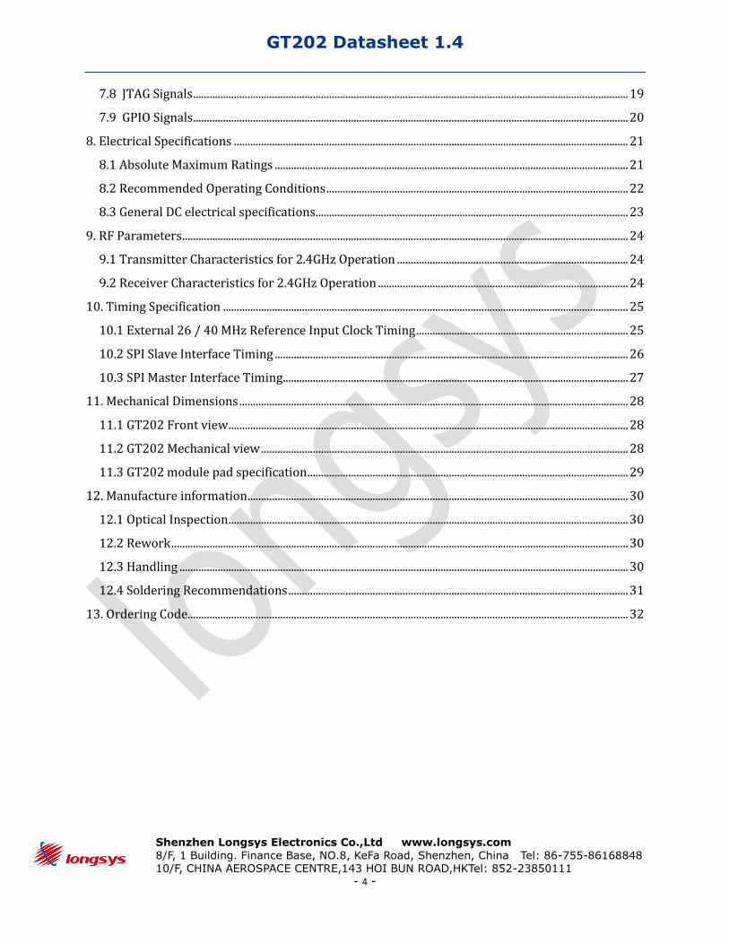
Index
1. Introduction ........................................................................................................................................................................... 5
1.1 General Description ..................................................................................................................................................... 5
1.2 Hardware Description ............................................................................................................................................... 5
1.3 Wireless Specification ............................................................................................................................................... 6
1.4 Performance Specification....................................................................................................................................... 6
1.5 Protocols ......................................................................................................................................................................... 6
1.6 Typical application ...................................................................................................................................................... 6
1.7 Warranty ......................................................................................................................................................................... 6
1.8 Certifications ................................................................................................................................................................. 6
2. System Block Diagram ....................................................................................................................................................... 7
3. Features ................................................................................................................................................................................... 8
3.1 IPv4/IPv6 Networking ............................................................................................................................................... 8
3.2 Power Management .................................................................................................................................................... 9
3.3 Application Program Interface ............................................................................................................................ 10
3.4 WiFi Link Feature ...................................................................................................................................................... 10
4. Mode of operations .......................................................................................................................................................... 11
4.1 SPI slave link mode ................................................................................................................................................... 11
5. Reference design platform ............................................................................................................................................ 12
6. GT202 Pin-out .................................................................................................................................................................... 13
6.1 Pin-out Top view ....................................................................................................................................................... 13
6.2 GT202 Pin Assignment and Descriptions ........................................................................................................ 14
6.3 GT202 Pin Functions ................................................................................................................................................ 15
7. GT202 Interface description ........................................................................................................................................ 16
7.1 Bootstrap signals ....................................................................................................................................................... 16
7.2 SPI slave signals ......................................................................................................................................................... 17
7.3 Quad SPI master signals ........................................................................................................................................ 17
7.4 SDIO signals ................................................................................................................................................................ 18
7.5 I²S signals .................................................................................................................................................................... 18
7.6 I²C signals .................................................................................................................................................................... 19
7.7 UART Signals ............................................................................................................................................................... 19
GT202 Datasheet 1.4
Shenzhen Longsys Electronics Co.,Ltd www.longsys.com
8/F, 1 Building. Finance Base, NO.8, KeFa Road, Shenzhen, China Tel: 86-755-86168848 10/F, CHINA AEROSPACE CENTRE,143 HOI BUN ROAD,HKTel: 852-23850111
- 4 -
7.8 JTAG Signals ................................................................................................................................................................ 19
7.9 GPIO Signals ................................................................................................................................................................ 20
8. Electrical Specifications ................................................................................................................................................. 21
8.1 Absolute Maximum Ratings .................................................................................................................................. 21
8.2 Recommended Operating Conditions ............................................................................................................... 22
8.3 General DC electrical specifications................................................................................................................... 23
9. RF Parameters .................................................................................................................................................................... 24
9.1 Transmitter Characteristics for 2.4GHz Operation ..................................................................................... 24
9.2 Receiver Characteristics for 2.4GHz Operation ............................................................................................ 24
10. Timing Specification ..................................................................................................................................................... 25
10.1 External 26 / 40 MHz Reference Input Clock Timing .............................................................................. 25
10.2 SPI Slave Interface Timing .................................................................................................................................. 26
10.3 SPI Master Interface Timing ............................................................................................................................... 27
11. Mechanical Dimensions ............................................................................................................................................... 28
11.1 GT202 Front view ................................................................................................................................................... 28
11.2 GT202 Mechanical view ....................................................................................................................................... 28
11.3 GT202 module pad specification ...................................................................................................................... 29
12. Manufacture information ............................................................................................................................................ 30
12.1 Optical Inspection ................................................................................................................................................... 30
12.2 Rework ........................................................................................................................................................................ 30
12.3 Handling ..................................................................................................................................................................... 30
12.4 Soldering Recommendations ............................................................................................................................. 31
13. Ordering Code .................................................................................................................................................................. 32

GT202 Datasheet 1.4
Shenzhen Longsys Electronics Co.,Ltd www.longsys.com
8/F, 1 Building. Finance Base, NO.8, KeFa Road, Shenzhen, China Tel: 86-755-86168848 10/F, CHINA AEROSPACE CENTRE,143 HOI BUN ROAD,HKTel: 852-23850111
- 5 -
1. Introduction
1.1 General Description The Longsys GT202 module with a built-in printed
antenna is an intelligent platform for the Internet
of Everything. This complete networking
platform enables customers to add full-featured
Wi-Fi to a wide variety of products with minimal
development effort and cost. It supports a
network stack along with SSL security, enabling
full-featured internet connectivity and reliable
information exchange in a small, low-cost system.
The GT202 provides two host interfaces for
connecting to local system controllers. A UART-
based host interface can be used for rapid
development and deployment of simple data
streams between the local device and the
internet cloud. A SPI slave interface is available
for applications that require more advanced
connectivity to the network. The reference
design platform will include an Arduino/Freedom
interface board (GT-202-EVB) to connect existing
micro controller reference platforms (eq
Freescale KL26 based FRDM-KL26Z Freedom
Development Platform) using a standardized
connectors.
The GT202 module contains a Qualcomm
QCA4002 chip. The QCA4002 is a single chip
system on a chip (SoC) 1x1 802.11 b/g/n device
optimized for low-power embedded applications
with single-stream capability for both Tx and Rx.
It has an integrated network processor with a
large set of TCP/IP with IPv4/IPv6-based services.
These services can be accessed via a serial SPI link
or by a UART link connected to an external host
CPU.
1.2 Hardware Description Size: 24 x 18 x 2.64 mm
Tolerance:0.3mm
Operating voltage: 3.3 V ± 10%
Operating humidity: 20-70%
Operating temperature range:
o Industrial: -40°C ~ +85°C
o Commercial: 0°C ~ +65°C
Connector: SMD-Pad connector - 26 Pads
Host interface: UART, SPI
o SPI slave: Allows simplified
connection to local host MCU.
Host driver and programming API
available from Qualcomm.
o UART interface: Supports AT style
command set.
GPIO suit for 1.8V or 3.3V:optional

GT202 Datasheet 1.4
Shenzhen Longsys Electronics Co.,Ltd www.longsys.com
8/F, 1 Building. Finance Base, NO.8, KeFa Road, Shenzhen, China Tel: 86-755-86168848 10/F, CHINA AEROSPACE CENTRE,143 HOI BUN ROAD,HKTel: 852-23850111
- 6 -
1.3 Wireless Specification Standard supported: IEEE802.11b/g/n
Frequency: 2.412 to 2.484GHz
Channels: up to 13 channels
1.4 Performance
Specification Host data rates
o UART: 115200, 8, n, 1, with actual
data rate to 100k bps
o SPI: up to 10 Mbps
1.5 Protocols Internet protocols: IPv4/IPv6, TCP/UDP,
ARP/NDP, DHCPv4, ICMPv6
Security protocols: WPS, WPA, WPA2,
WAPI, WEP, TKIP
1.6 Typical application
Household appliances
Gaming consoles
Handheld terminals
Embedded wireless products
Security monitoring Device
Industrial control
Home automation
1.7 Warranty One Year
1.8 Certifications CE
FCC
ROHS compliant

GT202 Datasheet 1.4
Shenzhen Longsys Electronics Co.,Ltd www.longsys.com
8/F, 1 Building. Finance Base, NO.8, KeFa Road, Shenzhen, China Tel: 86-755-86168848 10/F, CHINA AEROSPACE CENTRE,143 HOI BUN ROAD,HKTel: 852-23850111
- 7 -
2. System Block Diagram

GT202 Datasheet 1.4
Shenzhen Longsys Electronics Co.,Ltd www.longsys.com
8/F, 1 Building. Finance Base, NO.8, KeFa Road, Shenzhen, China Tel: 86-755-86168848 10/F, CHINA AEROSPACE CENTRE,143 HOI BUN ROAD,HKTel: 852-23850111
- 8 -
3. Features
3.1 IPv4/IPv6 Networking
The QCA4002 includes a TCP/IP and UDP offload capability. This capability can reduce Flash
requirements on a host MCU by up to 100 KBytes and also free up CPU cycles. The IP stack is a
simultaneous IPv4/IPv6 stack with a BSD-like interface to simplify porting and integration with
common embedded operating systems. The supported features of the QCA4002 (support for DHCP,
multicast, and ARP) include:
● ARP
● Forwarding
● Fragmentation/reassembly (supported with limitation)
● IPv4/v6 header processing
● UDP/TCP socket support
● DHCP v4
● Neighbor discovery
● Broadcast/multicast
● Path MTU discovery
● Address auto-configuration
● Multicast
● TCPzero-copy feature
QCA4002 IPv4 Supported RFCs
IPv4 RFC Number
RFC 1122 (TCP Timeout/retransmission)
RFC1122:TCP Keep-alive
RFC1122:TCP Zero-Window-Probe
RFC1122:TCP Sliding window protocol

GT202 Datasheet 1.4
Shenzhen Longsys Electronics Co.,Ltd www.longsys.com
8/F, 1 Building. Finance Base, NO.8, KeFa Road, Shenzhen, China Tel: 86-755-86168848 10/F, CHINA AEROSPACE CENTRE,143 HOI BUN ROAD,HKTel: 852-23850111
- 9 -
QCA4002 IPv4 Supported RFCs
IPv6 RFC Number
RFC-2464:Transmission of IPv6 packets over Ethernet networks
RFC-2460:Internet Protocol version 6
RFC2462, Duplicate Address Detection (DAD)
RFC-2463:ICMPv6
RFC3513:IP version 6 addressing architecture
RFC3484:Default Address Selection
RFC2461:Neighbour discovery for IPv6 host
RFC4862:Stateless Address Auto-configuration
3.2 Power Management
GT202provides integrated power management and control functions and extremely low power
operation for maximum battery life across all operational states.
o Power saving mode: 1.09 mA(DTIM=1)
o Standby mode(Sleep): 130uA
Sleep state minimizes power consumption while network services are not required, yet the system
needs to remain available for use within a short time.

GT202 Datasheet 1.4
Shenzhen Longsys Electronics Co.,Ltd www.longsys.com
8/F, 1 Building. Finance Base, NO.8, KeFa Road, Shenzhen, China Tel: 86-755-86168848 10/F, CHINA AEROSPACE CENTRE,143 HOI BUN ROAD,HKTel: 852-23850111
- 10 -
3.3 Application Program Interface
APIs provided by Qualcomm enable flexible host application customization. The firmware is written,
owned, controlled, and maintained by Qualcomm, whereas the reference host software is supplied
for system integrator to create application-specific host software, or even to use without
modification.
Note: If system integrator leverages the Qualcomm host software components, ultimately the
system developer is responsible for the host software on their platforms, OSes, and interconnects.
3.4 WiFi Link Feature
IEEE 802.11b/g/n, single stream 1x1
Single-band 2.4 GHz
Integrated PA, LNA, with support for external PA and external LNA
Single Rx front end for multiple applications
Green Tx power saving mode
Low power listen mode
Two-layer PCB design
Link rates up to 150 Mbps
State Typical Current Consumption for GT202 module
SUSPEND 6uA
SLEEP 130uA
802.11g
(2.4GHz)
DTIM1 1,090uA
DTIM3 473uA
DTIM5 335uA
DTIM10 258uA

GT202 Datasheet 1.4
Shenzhen Longsys Electronics Co.,Ltd www.longsys.com
8/F, 1 Building. Finance Base, NO.8, KeFa Road, Shenzhen, China Tel: 86-755-86168848 10/F, CHINA AEROSPACE CENTRE,143 HOI BUN ROAD,HKTel: 852-23850111
- 11 -
4. Mode of operations
4.1 SPI slave link mode
GT202module can be configured to support SPI slave interface to a host CPU as well. In this mode,
GT202 can provide full network functionalities.

GT202 Datasheet 1.4
Shenzhen Longsys Electronics Co.,Ltd www.longsys.com
8/F, 1 Building. Finance Base, NO.8, KeFa Road, Shenzhen, China Tel: 86-755-86168848 10/F, CHINA AEROSPACE CENTRE,143 HOI BUN ROAD,HKTel: 852-23850111
- 12 -
5. Reference design platform The GT202 reference design platform will include an Arduino/Freedom interface board (GT-202-EVB) to
connect existing micro controller reference platforms (eq Freescale KL26 based FRDM-KL26Z Freedom
Development Platform) using a standardized connectors.

GT202 Datasheet 1.4
Shenzhen Longsys Electronics Co.,Ltd www.longsys.com
8/F, 1 Building. Finance Base, NO.8, KeFa Road, Shenzhen, China Tel: 86-755-86168848 10/F, CHINA AEROSPACE CENTRE,143 HOI BUN ROAD,HKTel: 852-23850111
- 13 -
6. GT202 Pin-out
6.1 Pin-out Top view
Dimension Label
Dimension (mm)
A 2.5
B 2.0
C 2.0
D 18
E 24
Module Height 2.5

GT202 Datasheet 1.4
Shenzhen Longsys Electronics Co.,Ltd www.longsys.com
8/F, 1 Building. Finance Base, NO.8, KeFa Road, Shenzhen, China Tel: 86-755-86168848 10/F, CHINA AEROSPACE CENTRE,143 HOI BUN ROAD,HKTel: 852-23850111
- 14 -
6.2 GT202 Pin Assignment and Descriptions
Signal Name Pin Description
USB_DP 12 USB device / manufacturing test and configuration interface
USB_DN 13
CHIP_PWD# 19 Power down control signal; setting this pin low forces the module in to its lowest power state
TDO 1 GPIO with multiplexed functions.
TCK/I2C_CLK 2
UART1_TXD/I2S0_BCK/TM 3
UART1_RXD/I2S0_MCK/TMS 4
I2C_DATA/TDI 7
SPI_CLK/SD_CLK/I2S1_MCK 8
SPI_MISO/SD_D0/I2S1_WS/JTAG_EN 10
SPI_INT/SD_D1/I2S1_SDO 14
SD_D2/I2S1_SDI/HM0 15
SPI_MOSI/SD_D3/I2S1_BCK 16
SPI_CS/SD_CMD/HM1 17
UART0_CTS 21
I2S0_WS 22
UART0_RTS 23
UART0_TXD/I2S0_SDI 24
UART0_RXD/I2S0_SDO/TRST 25
GND 5,9,18,26 Ground
VDDIO_SDIO 6 3.3V supply for SDIO
3.3V 11 Analog 3.3Vsupply
DVDD_GPIO 20 VDDIO 3.3Vsupply for GPIOs

GT202 Datasheet 1.4
Shenzhen Longsys Electronics Co.,Ltd www.longsys.com
8/F, 1 Building. Finance Base, NO.8, KeFa Road, Shenzhen, China Tel: 86-755-86168848 10/F, CHINA AEROSPACE CENTRE,143 HOI BUN ROAD,HKTel: 852-23850111
- 15 -
6.3 GT202 Pin Functions
Bootstrap Alt1 Alt2 Alt3 Alt4 Alt5
1 EN_LINEAR GPIO13 GPIO13 GPIO13 GPIO13 TDO
2 - I2C_CLK I2C_CLK 12C_CLK 12C_CLK TCK
3 TEST_MODE UART1_TXD UART1_TXD I2S0_BCK I2S0_BCK GPIO11
4 - UART1_RXD UART1_RXD I2S0_MCK I2S0_MCK TMS
7 - I2_DATA I2C_DATA I2C_DATA I2C_DATA TDI
8 - SPI_CLK SD_CLK SPI_CLK I2S1_MCK SPI_CLK
10 EJTAG_SEL SPI_MISO SD_D0 SPI_MISO I2S1_WS SPI_MISO
14 - SPI_INT SD_D1 SPI_INT I2S1_SDO SPI_INT
15 HM0 GPIO2 SD_D2 GPIO2 I2S1_SDI GPIO2
16 - SPI_MOSI SD_D3 SPI_MOSI I2S1_BCK SPI_MOSI
17 HM1 SPI_CS SD_CMD SPI_CS GPIO0 SPI_CS
21 - UART0_CTS UART0_CTS GPIO23 GPIO23 GPIO23
22 - GPIO21 GPIO21 I2S0_WS I2S0_WS GPIO21
23 - UART0_RTS UART0_RTS GPIO22 GPIO22 GPIO22
24 - UART0_TXD UART0_TXD I2S0_SDI I2S0_SDI UART0_TXD
25 - UART0_RXD UART0_RXD I2S0_SDO I2S0_SDO TRST

GT202 Datasheet 1.4
Shenzhen Longsys Electronics Co.,Ltd www.longsys.com
8/F, 1 Building. Finance Base, NO.8, KeFa Road, Shenzhen, China Tel: 86-755-86168848 10/F, CHINA AEROSPACE CENTRE,143 HOI BUN ROAD,HKTel: 852-23850111
- 16 -
7. GT202 Interface description
7.1 Bootstrap signals
Signal Name
Direction while
CHIP_PWD#
Is low
Description
ENLINEAR2 I
Bootstrap for 1.2V regulator mode. This pin be pulled low to select the switching regulator mode used on the GT202
module. Note :The pull-up or pull-down resistor is populated on the module. The system level should take care not to conflict with pull selection on the module.
TESTMODE
EJTAGSEL3 I
Bootstrap for on board CPU debug(JTAG CPU debug mode).The system must pull both pins to 1 to invoke
debug mode(EJTAG mode operation).The system must pull TESTMODE to 0 to boot up in non-CPU JTAG debug
mode.
HM[1:0]3
I
Bootstrap for host interface selection.
Note: The pull-up or pull-down resistor is populated on the module. The system level should take care not to
conflict with pull selection on the module.
Pull to 00 Enter USB/manufacturing test and configuration mode
Pull to 01 Enter No External Host Required mode
Pull to 10 Enter SPI Host mode
Pull to 11 Enter SDIO Host mode

GT202 Datasheet 1.4
Shenzhen Longsys Electronics Co.,Ltd www.longsys.com
8/F, 1 Building. Finance Base, NO.8, KeFa Road, Shenzhen, China Tel: 86-755-86168848 10/F, CHINA AEROSPACE CENTRE,143 HOI BUN ROAD,HKTel: 852-23850111
- 17 -
7.2 SPI slave signals
Signal Name Direction Description
SPI_CLK I Clock line from master, maximum rate 48 MHz
SPI_CS I Chip select, active low
SPI_INT O Active low interrupt to SPI master controller
SPI_MISO O Serial data to master
SPI_MOSI I Serial data from master
7.3 Quad SPI master signals These signals enable the QCA4002 to boot from an external SPI flash device. The QCA4002 supports single/quad mode SPI flash read/write.
Signal Name Direction Description
SPIM_CLK O SPI serial interface clock
SPIM_CS O SPI chip select
SPIM_MISO IO Data transmission from the QCA4002 to an external device
SPIM_MOSI IO Data transmission from an external device to the QCA4002
SPIM_WP IO Write protection. Used as IO2 in Quad mode.

GT202 Datasheet 1.4
Shenzhen Longsys Electronics Co.,Ltd www.longsys.com
8/F, 1 Building. Finance Base, NO.8, KeFa Road, Shenzhen, China Tel: 86-755-86168848 10/F, CHINA AEROSPACE CENTRE,143 HOI BUN ROAD,HKTel: 852-23850111
- 18 -
7.4 SDIO signals
Signal Name Direction Description
SD_CLK I SDYO I dock from host
SD_CMD IO SDIO command line
SD_DATA(0) IO SDIO data lines
SD_DATA(1) IO
SD_DATA(2) IO
SD_DATA(3) IO
7.5 I²S signals
Signal Name Direction Description
I2S0BCK I Stereo clock
I2S0MCK Master clock
I2S0SDI I Serial data I
I2S0SDO O Serial data O
I2S0WS O Word select for stereo
0 Left
1 Right
I2S1_BCK I Stereo clock
I2S1_MCK Master clock
I2S_SDI I Serial data I
I2S1_SDO O Serial data O
I2S1_WS O Word select for stereo
0 Left
1 Right

GT202 Datasheet 1.4
Shenzhen Longsys Electronics Co.,Ltd www.longsys.com
8/F, 1 Building. Finance Base, NO.8, KeFa Road, Shenzhen, China Tel: 86-755-86168848 10/F, CHINA AEROSPACE CENTRE,143 HOI BUN ROAD,HKTel: 852-23850111
- 19 -
7.6 I²C signals
Signal Name
Direction
Description
I2C-CLK IO I2C clock
I2-DATA IO I2C data
7.7 UART Signals
Signal Name Direction Description
UART0_CTS I UART clear to send signal
UART0_RTS O UART ready to send signal
UART0_RXD I UART receive data
UART0_TXD O UART transmit data
UART1_RXD I UART receive data
UART1_TXD O UART transmit data
7.8 JTAG Signals
Signal Name Direction Description
TCK I JTAG clock
TDI I JTAG data I
TDO O JTAG data O
TMS I JTAG mode select
TRST I Warm reset

GT202 Datasheet 1.4
Shenzhen Longsys Electronics Co.,Ltd www.longsys.com
8/F, 1 Building. Finance Base, NO.8, KeFa Road, Shenzhen, China Tel: 86-755-86168848 10/F, CHINA AEROSPACE CENTRE,143 HOI BUN ROAD,HKTel: 852-23850111
- 20 -
7.9 GPIO Signals
Signal Name Direction Description
GPIO0 I/O General purpose input/output.
The QCA4002 supports SDIO,SPI,I2C,I2S,UART,and JTAG interfaces.It is possible to configure the QCA4002 to support
these interfaces by tying certain inputs externally during boot up.
GPIO2 I/O
GPIo11 I/O
GPIO13 I/O
GPIO21 I/O
GPIO22 I/O
GPIO23 I/O

GT202 Datasheet 1.4
Shenzhen Longsys Electronics Co.,Ltd www.longsys.com
8/F, 1 Building. Finance Base, NO.8, KeFa Road, Shenzhen, China Tel: 86-755-86168848 10/F, CHINA AEROSPACE CENTRE,143 HOI BUN ROAD,HKTel: 852-23850111
- 21 -
8. Electrical Specifications
8.1 Absolute Maximum Ratings Table 8-1 summarizes the absolute maximum ratings and Table 8-2 lists the recommended
operating conditions for the GT202. Absolute maximum ratings are those values beyond which
damage to the device can occur.
Functional operation under these conditions, or at any other condition beyond those indicated inthe
operational sections of this document, is not recommended.
NOTE Maximum rating for signals follows the supply domain of the signals.
Table 8-1 absolute maximum ratings
symbol Description Max rating unit
VDDIO_HOST VDD supply for
interface –0.3 to 4.0 V
DVDD_GPIO VDD supply for GPIOs –0.3 to 4.0 V
VDD33
VDD supply for whole
module –0.3 to 4.0 V
VIH MIN
Minimum Digital I/O
Input Voltage for 1.8 V
or 3.3 V I/O Supply
–0.3 V
3.3 V I/O VIH MAX
Maximum Digital I/O
Input Voltage for 3.3 V
I/O Supply
Vdd +0.3 V
RFin
Maximum RF input
(reference to 50-Ω
input)
+10 dbm
Tstore Storage Temperature –45 to 135 °C
Tj Junction Temperature 125 °C
ESD Electrostatic Discharge
Tolerance
HBM - 2000
CDM - 500 V

GT202 Datasheet 1.4
Shenzhen Longsys Electronics Co.,Ltd www.longsys.com
8/F, 1 Building. Finance Base, NO.8, KeFa Road, Shenzhen, China Tel: 86-755-86168848 10/F, CHINA AEROSPACE CENTRE,143 HOI BUN ROAD,HKTel: 852-23850111
- 22 -
8.2 Recommended Operating Conditions These conditions apply to all DC characteristics unless otherwise specified:
Tamb = 25 °C, Vdd33= 3.3 V
Table 8-2 Recommended Operating Conditions
Symbol Parameter Min Typ Max unit
VDDIO_HOST VDD supply for
interface
3.0 - 3.46 V
DVDD_GPIO VDD supply for
GPIOs
1.71 - 3.46 V
VDD33 VDD supply for
whole module
3.14 3.3 3.46 V
Tcase Case
temperature 0 - 85 °C
PsiJT Thermal
Parameter2
-
3 - °C/W

GT202 Datasheet 1.4
Shenzhen Longsys Electronics Co.,Ltd www.longsys.com
8/F, 1 Building. Finance Base, NO.8, KeFa Road, Shenzhen, China Tel: 86-755-86168848 10/F, CHINA AEROSPACE CENTRE,143 HOI BUN ROAD,HKTel: 852-23850111
- 23 -
8.3 General DC electrical specifications These conditions apply to all DC characteristics unless otherwise specified:
Tamb = 25℃, Vdd33= 3.3 V
Table 8-3 DC Electrical Characteristics for Digital I/Os
Symbol Parameter Conditions Min Typ Max Unit
VIH High level voltage 1.8 3.6 V
VIL Low level voltage -0.3 0.3 V
VOH High level O voltage 2.2 3.3 V
VOL Low level O voltage 0 0.4 V
IIL Low level I current 0.1 uA
IOH High level O current for GPIO0 to GPIO13 8 mA
High level O current for GPIO18 to GPIO25 20
IIH High level I current 0.1 uA
IOL High level O current for GPIO0 to GPIO13 20 mA
High level O current for GPIO18 to GPIO25 20
CIN I capacitance for GPIO0 to GPIO13 5 pF
I capacitance for GPIO18 to GPIO25 3

GT202 Datasheet 1.4
Shenzhen Longsys Electronics Co.,Ltd www.longsys.com
8/F, 1 Building. Finance Base, NO.8, KeFa Road, Shenzhen, China Tel: 86-755-86168848 10/F, CHINA AEROSPACE CENTRE,143 HOI BUN ROAD,HKTel: 852-23850111
- 24 -
9. RF Parameters
9.1 Transmitter Characteristics for 2.4GHz Operation Table 9-1 summarizes the transmitter characteristics for the GT202.
Table 9-1 transmitter characteristics
Symbol Rate/Mbps IEEE Citation Output power/dbm
802.11b 11 18.4.7.2 18±3
802.11g 6 17.3.9.1 18±3
54 17.3.9.1 14±3
802.11n 6.5 20.3.21.3 18±3
135 20.3.21.3 13±3
9.2 Receiver Characteristics for 2.4GHz Operation
Table 9-2 summarizes the receiver characteristics for the GT202. Notice that transmitter and
especially receiver characteristics must be test under test guider.
Table 8-2 receiver characteristics
Symbol Rate/Mbps IEEE limited/dbm Typical Sensitivity/dbm
802.11 b 11 -76 -82
802.11g 6 -82 -85
54 -65 -68
802.11n 6.5 -82 -85
135 -61 -64

GT202 Datasheet 1.4
Shenzhen Longsys Electronics Co.,Ltd www.longsys.com
8/F, 1 Building. Finance Base, NO.8, KeFa Road, Shenzhen, China Tel: 86-755-86168848 10/F, CHINA AEROSPACE CENTRE,143 HOI BUN ROAD,HKTel: 852-23850111
- 25 -
10. Timing Specification
10.1 External 26 / 40 MHz Reference Input Clock Timing
Figure 10-1 External 40 MHz Reference Input
Table 10-1 External 26/40 MHz Reference Input Clock Timing
Symbol Description Min Typ Max Unit
CK1 Frequency accuracy -20 - 20 ppm
Frequency - 40 - MHz
CK2 Fall time 0.1 x period ns
CK3 Rise time 0.1 x period ns
CK4 Duty cycle(high-to-low ratio) 40 60 %
CK5 Input high voltage 0.75 1.26 V
CK6 Input low voltage -0.55 0.3 V

GT202 Datasheet 1.4
Shenzhen Longsys Electronics Co.,Ltd www.longsys.com
8/F, 1 Building. Finance Base, NO.8, KeFa Road, Shenzhen, China Tel: 86-755-86168848 10/F, CHINA AEROSPACE CENTRE,143 HOI BUN ROAD,HKTel: 852-23850111
- 26 -
10.2 SPI Slave Interface Timing
Figure 10-2 SPI Slave Timing
Table 10-2 SPI Slave Timing Constraints
Parameter Description Min Max Unit
fPP Clock frequency 0 48 MHz
tWL Clock low time 8.3 - ns
tWH Clock high time 8.33 - ns
tTLH Clock rise time - 2 ns
tTHL Clock fall time - 2 ns
tlSU Input setup time 5 - ns
tlH Input hold time 5 - ns
tO_DLY Output delay 0 5 ns

GT202 Datasheet 1.4
Shenzhen Longsys Electronics Co.,Ltd www.longsys.com
8/F, 1 Building. Finance Base, NO.8, KeFa Road, Shenzhen, China Tel: 86-755-86168848 10/F, CHINA AEROSPACE CENTRE,143 HOI BUN ROAD,HKTel: 852-23850111
- 27 -
10.3 SPI Master Interface Timing
Figure 10-3 SPI Master Timing
Table 10-3 SPI Master Timing Constraints
Parameter Description Min Max Unit
tCP Clock period 30.7 1000 ns
tCSD Chip select valid delay -5.5 5 ns
tDD Date valid delay -5.5 5 ns
tDS Data setup 3 - ns
tDH Data hold 0 - ns

GT202 Datasheet 1.4
Shenzhen Longsys Electronics Co.,Ltd www.longsys.com
8/F, 1 Building. Finance Base, NO.8, KeFa Road, Shenzhen, China Tel: 86-755-86168848 10/F, CHINA AEROSPACE CENTRE,143 HOI BUN ROAD,HKTel: 852-23850111
- 28 -
11. Mechanical Dimensions
11.1 GT202 Front view
11.2 GT202 Mechanical view

GT202 Datasheet 1.4
Shenzhen Longsys Electronics Co.,Ltd www.longsys.com
8/F, 1 Building. Finance Base, NO.8, KeFa Road, Shenzhen, China Tel: 86-755-86168848 10/F, CHINA AEROSPACE CENTRE,143 HOI BUN ROAD,HKTel: 852-23850111
- 29 -
11.3 GT202 module pad specification
PAD Locations
Parameter Description Value(mm)
A Pin Exterior 1.22
B Pin Interior Diameter 0.508
C Pin Interior Offset 0.356
D Pin Spacing 0.78
E Pin Exterior 0.61
F Pin Comer Spacing 1.5

GT202 Datasheet 1.4
Shenzhen Longsys Electronics Co.,Ltd www.longsys.com
8/F, 1 Building. Finance Base, NO.8, KeFa Road, Shenzhen, China Tel: 86-755-86168848 10/F, CHINA AEROSPACE CENTRE,143 HOI BUN ROAD,HKTel: 852-23850111
- 30 -
12. Manufacture information
12.1 Optical Inspection After SMT, GT202 PCBA will be automatically sent to do AOI(Automatic Optic Inspection). Longsys uses
TR7500 to check every PCBA.
TR7500features:
3CCD camera with 5 detectors
All pictures have the sense of 3D
Resolution: 10μm
TR7500 can detect blemishes during SMT to guarantee quality at the first step before IOE and fully
functional test.
12.2 Rework
The module can be unsoldered from the host board if the Moisture Sensitivity Level (MSL) requirements
are met as described in this datasheet. Never attempt a rework on the module itself, e.g. replacing
individual components. Such actions will terminate warranty coverage.
12.3 Handling
TheGT202modules contain a highly sensitive electronic circuitry. Handling without proper ESD
protection may destroy or damage the module permanently.

GT202 Datasheet 1.4
Shenzhen Longsys Electronics Co.,Ltd www.longsys.com
8/F, 1 Building. Finance Base, NO.8, KeFa Road, Shenzhen, China Tel: 86-755-86168848 10/F, CHINA AEROSPACE CENTRE,143 HOI BUN ROAD,HKTel: 852-23850111
- 31 -
12.4 Soldering Recommendations
TheGT202modules can be SMT on the board following the temperature curve graph :

GT202 Datasheet 1.4
Shenzhen Longsys Electronics Co.,Ltd www.longsys.com
8/F, 1 Building. Finance Base, NO.8, KeFa Road, Shenzhen, China Tel: 86-755-86168848 10/F, CHINA AEROSPACE CENTRE,143 HOI BUN ROAD,HKTel: 852-23850111
- 32 -
13. Ordering Code GT202 - W X Y ZZZ
Firmware version
Hardware version
Antenna code
Chip code
Chip code
Code Description
I QCA4002X-AL3B, I-Temp
C QCA4002X-AL3A, C-Temp
G QCA4002X-BL3B, I-Temp
L QCA4002X-BL3A, C-Temp
Antenna code
Code Description
C Internal PCB antenna
I IPex Socket, External antenna
P Ceramic Chip antenna

GT202 Datasheet 1.4
Shenzhen Longsys Electronics Co.,Ltd www.longsys.com
8/F, 1 Building. Finance Base, NO.8, KeFa Road, Shenzhen, China Tel: 86-755-86168848 10/F, CHINA AEROSPACE CENTRE,143 HOI BUN ROAD,HKTel: 852-23850111
- 33 -
Hardware version
Code Description
0 V1.02
1 V1.03
2 V1.04 (GT202-030)
3 V1.05 (GT202-100)
4 V1.06 (GT202-110)
5 V1.07 (GT202-120)
Firmware version
Code Description
005 R3.2.0.0.173
006 R3.0.2.14.56
007 R3.3

![MANUAL DE PROGRAMACIÓN - weg. · PDF file15.3 Protecciones [45].....15-4 15.4 Protección de Sobretemperatura del Motor Usando Módulo IOE -01, IOE-02 o IOE-03 .....15-17 15.4.1](https://img.pdfslide.tips/doc/110x75/5a7ebd607f8b9a0a668f0a4a/manual-de-programacin-weg-153-protecciones-4515-4-154-proteccin-de.jpg)