Embed Size (px)
Citation preview
1772 IEEE JOURNAL OF SELECTED TOPICS IN QUANTUM ELECTRONICS, VOL. 17, NO. 6, NOVEMBER/DECEMBER 2011
Heat Management in High-PowerVertical-External-Cavity Surface-Emitting Lasers
Alexej Chernikov, Jens Herrmann, Martin Koch, Bernardette Kunert, Wolfgang Stolz, Sangam Chatterjee, StephanW. Koch, Tsuei-Lian Wang, Yushi Kaneda, J. Michael Yarborough, Jorg Hader, and Jerome V. Moloney
Abstract—The thermal properties of a high-power vertical-external-cavity surface-emitting laser (VECSEL) are studied ex-perimentally, focusing on the generation, distribution, and removalof excess heat under extreme pumping conditions. Different heat-spreading and heat-transfer approaches are analyzed. The per-formance of the device is optimized yielding a maximum emittedpower beyond 70 W from a single spot. Finally, the potential forpower-scaling in VECSELs and its restrictions are examined.
Index Terms—High-power operation, thermal properties,VECSEL.
I. INTRODUCTION
OVER the last decade, vertical-external-cavity surface-emitting lasers (VECSELs) have received much attention
in the scientific community. Developed in the late 1990s [11],[17] this particular type of the semiconductor laser perfectlycombines the excellent beam quality of surface emitters andthe high output power of semiconductor edge-emitting diodelasers [17]. In addition, solid-state on-chip fabrication, smallpackaging dimensions, and the spectral tunability are all main-tained as the main advantages of a semiconductor device. VEC-SELs are available in a broad spectral range [4], [8], [24],[26], [27]. They offer efficient intracavity frequency mixing [3],[7], [14], [18], [23] combined with frequency stabilization [12],and are able to operate in a pulsed regime, emitting ultra shortsub-500-fs pulses [9], [10], [13], [29]. For the majority of the
Manuscript received November 30, 2010; revised January 5, 2011; acceptedJanuary 13, 2011. Date of publication April 29, 2011; date of current versionDecember 7, 2011. This work was supported in part by the U.S. Joint Technol-ogy Office Multidisciplinary Research Initiative Program under Grant AFOSRFA9550-07-1-0573, in part by the Deutsche Forschungsgemeinschaft, and inpart by the Humboldt Foundation.
A. Chernikov, J. Herrmann, M. Koch, W. Stolz, S. Chatterjee, and S. W.Koch are with the Faculty of Physics and Materials Sciences Center, Philipps-Universitat Marburg, D-35032 Marburg, Germany (e-mail: [email protected]; [email protected]; [email protected]; [email protected]; [email protected]; [email protected]).
B. Kunert is with the NAsP III/V GmbH, 35041 Marburg, Germany (e-mail:[email protected]).
T.-L. Wang, Y. Kaneda, and J. M. Yarborough are with the Collegeof Optical Sciences, The University of Arizona, Tucson, AZ 85721 USA(e-mail: [email protected]; [email protected]; [email protected]).
J. Hader and J. V. Moloney are with the College of Optical Sciences, TheUniversity of Arizona, Tucson, AZ 85721 USA, and also with NonlinearControl Strategies, Inc., Tuscon, AZ 85705 USA ([email protected];[email protected]).
Color versions of one or more of the figures in this paper are available onlineat http://ieeexplore.ieee.org.
Digital Object Identifier 10.1109/JSTQE.2011.2115995
applications, however, high output power of the device remainscrucial.
The performance of the VECSEL is generally limited byoverheating. The latter leads to a so-called thermal rollover—a rapid decrease of the output power even when the pump isincreased. The excess heat is generated inside of the VEC-SEL chip due to the intrinsic properties of the active structureand off-resonant pumping conditions required for laser oper-ation [22], [25]. Therefore, efficient cooling concepts are in-evitable for the high-power operation. Fortunately, VECSELchips offer a potentially large active area and are therefore pro-posed to achieve higher output power by simply increasing thesize of the pump spot [6], [19], [21], [27]. However, this powerscalability is questioned in several reports, at least for specificpumping conditions [1], [20], [28]. Possible reasons for this be-havior are inhomogeneous loss-channel distribution due to thegrowth and processing imperfections or substantial importanceof 3-D heat transfer in the structure [1], [28].
In this paper, we focus on the study of thermal properties of ahigh-power VECSEL. We address the distribution and removalof excess heat and optimize the device for increased perfor-mance. Different heat-spreading and heat-transfer approachesare investigated experimentally. Based on these investigations,we evaluate the possibility for power scaling and analyze theunderlying restrictions.
II. EXPERIMENT
The investigated VECSEL device is designed for the opera-tion in the near-infrared spectral range at about 1040 nm. Thesemiconductor structure is grown using metal-organic vaporphase epitaxy and the so-called upside-down approach. First,an (GaIn)P window of about 150-nm thickness is deposited ona 650-μm-thick GaAs wafer. The active region consists of ten(GaIn)As quantum wells placed between GaAs buffer layers andGa(AsP) barriers for strain compensation and pump absorption,respectively. The quantum wells are arranged in a resonant-periodic-gain configuration, i.e., their spatial positions overlapwith the field maxima of the lasing mode. A high-reflectivitydistributed Bragg reflector (DBR) with 20 pairs of GaAs/AlAsis grown on top of the structure. For efficient heat transfer, thedevice is soldered to a heat spreader using an indium layer ofseveral microns thickness. Afterward, the GaAs substrate is re-moved by chemical etching. No antireflective coating is appliedto fully exploit the enhanced coupling of the material gain to thecavity mode for optimal high-power performance [2], [16], [22].
The VECSEL chip is mounted on a Peltier-cooled copperheat sink, its backside being held at 15 ◦C by closed-cycle water
1077-260X/$26.00 © 2011 IEEE
CHERNIKOV et al.: HEAT MANAGEMENT IN HIGH-POWER VECSELs 1773
cooling. The device is operated in a standard linear cavity of6-cm length using an output coupler with 10-cm radius of cur-vature and a transmission of 5%. This configuration supportsmany higher transversal modes, allowing spatially extendedpump spots and thus high output power [25]. A fiber-coupleddiode laser emitting a maximum output power of 400 W at808 nm is used as a pump source. The angle of incidence isset below 30◦ to obtain an only slightly elliptical pump spot.A charge-coupled-device-based beam profiler and an externalhigh-resolution digital camera are used to control the size andshape of the tailored pump profiles, obtained by appropriatepump optics. The output power is detected by a power meter ca-pable of measuring up to 200 W. Additionally, we use imagingoptics and a fiber-coupled optical spectrum analyzer to detectspatially resolved photoluminescence (PL) during device opera-tion. Experimental details on the PL setup are given in a previouswork [5].
III. RESULTS AND DISCUSSION
A. Heat Spread
Efficient cooling of the device strongly relies on heat spread-ing, the efficient distribution of the heat generated in the smallarea excited by the pump spot. Two properties are crucial for anoptimal heat-spreader: high thermal conductivity and low sur-face roughness, providing a smooth interface with the semicon-ductor device. In this section, we study two different materialsto optimize the heat-spreading properties of the structure forthe pump spot width of 300 μm. Chemically grown diamondand high-purity copper are both obvious choices for distributingthe heat due to their large thermal conductivities. For the ex-periments, two samples are chosen, 5 mm × 5 mm large plate,bonded to VECSEL chips from the same wafer. The advan-tage of diamond is its extremely high thermal conductivity of1800 W m−1 K−1 compared to about 400 W m−1 K−1 in copper.On the other hand, the lower cost and easier processing favorthe use of copper as a heat-sink material.
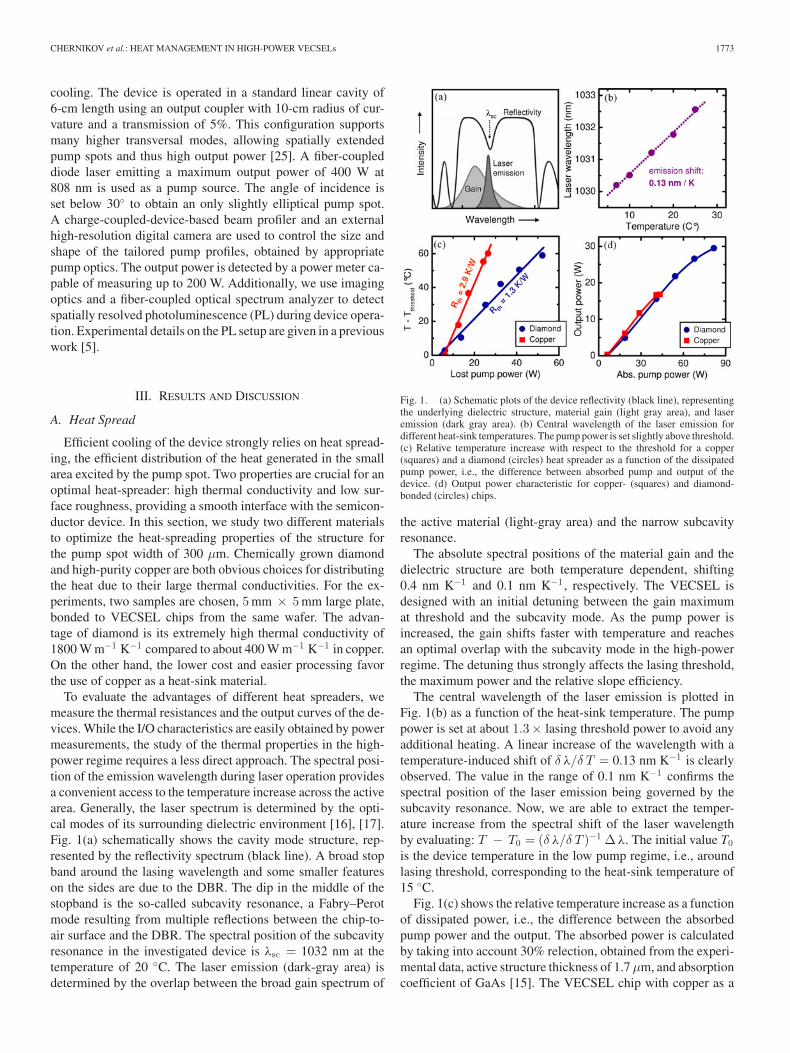
To evaluate the advantages of different heat spreaders, wemeasure the thermal resistances and the output curves of the de-vices. While the I/O characteristics are easily obtained by powermeasurements, the study of the thermal properties in the high-power regime requires a less direct approach. The spectral posi-tion of the emission wavelength during laser operation providesa convenient access to the temperature increase across the activearea. Generally, the laser spectrum is determined by the opti-cal modes of its surrounding dielectric environment [16], [17].Fig. 1(a) schematically shows the cavity mode structure, rep-resented by the reflectivity spectrum (black line). A broad stopband around the lasing wavelength and some smaller featureson the sides are due to the DBR. The dip in the middle of thestopband is the so-called subcavity resonance, a Fabry–Perotmode resulting from multiple reflections between the chip-to-air surface and the DBR. The spectral position of the subcavityresonance in the investigated device is λsc = 1032 nm at thetemperature of 20 ◦C. The laser emission (dark-gray area) isdetermined by the overlap between the broad gain spectrum of
Fig. 1. (a) Schematic plots of the device reflectivity (black line), representingthe underlying dielectric structure, material gain (light gray area), and laseremission (dark gray area). (b) Central wavelength of the laser emission fordifferent heat-sink temperatures. The pump power is set slightly above threshold.(c) Relative temperature increase with respect to the threshold for a copper(squares) and a diamond (circles) heat spreader as a function of the dissipatedpump power, i.e., the difference between absorbed pump and output of thedevice. (d) Output power characteristic for copper- (squares) and diamond-bonded (circles) chips.
the active material (light-gray area) and the narrow subcavityresonance.
The absolute spectral positions of the material gain and thedielectric structure are both temperature dependent, shifting0.4 nm K−1 and 0.1 nm K−1 , respectively. The VECSEL isdesigned with an initial detuning between the gain maximumat threshold and the subcavity mode. As the pump power isincreased, the gain shifts faster with temperature and reachesan optimal overlap with the subcavity mode in the high-powerregime. The detuning thus strongly affects the lasing threshold,the maximum power and the relative slope efficiency.
The central wavelength of the laser emission is plotted inFig. 1(b) as a function of the heat-sink temperature. The pumppower is set at about 1.3× lasing threshold power to avoid anyadditional heating. A linear increase of the wavelength with atemperature-induced shift of δ λ/δ T = 0.13 nm K−1 is clearlyobserved. The value in the range of 0.1 nm K−1 confirms thespectral position of the laser emission being governed by thesubcavity resonance. Now, we are able to extract the temper-ature increase from the spectral shift of the laser wavelengthby evaluating: T − T0 = (δ λ/δ T )−1 Δ λ. The initial value T0is the device temperature in the low pump regime, i.e., aroundlasing threshold, corresponding to the heat-sink temperature of15 ◦C.
Fig. 1(c) shows the relative temperature increase as a functionof dissipated power, i.e., the difference between the absorbedpump power and the output. The absorbed power is calculatedby taking into account 30% relection, obtained from the experi-mental data, active structure thickness of 1.7 μm, and absorptioncoefficient of GaAs [15]. The VECSEL chip with copper as a

1774 IEEE JOURNAL OF SELECTED TOPICS IN QUANTUM ELECTRONICS, VOL. 17, NO. 6, NOVEMBER/DECEMBER 2011
heat spreader heats up significantly faster than the diamond-bonded device. Thermal resistance R is obtained by extractingthe slope of the plotted curves yielding Rc = 2.5 K W−1 andRd = 1.3 K W−1 for copper and diamond heat spreaders, respec-tively. Even though diamond turns out to be clearly superior tocopper, the ratio of thermal resistances Rc /Rd = 1.9 is signifi-cantly lower than expected from the thermal conductivity ratioof 4.5 for the two materials.
The output-power characteristics plotted in Fig. 1(d) supportthe obtained results. The slope efficiency is equal for the twochips, indicating comparable loss channels in both devices. Thethermal rollover, however, occurs at about a factor of two higheroutput power in the diamond-soldered VECSEL, confirming itssuperior performance as a heat spreader.
B. Heat Removal
Eventually, the heat has to be transferred into the heat sink af-ter it is distributed across a large area of the heat spreader to keepthe temperature of the device below its thermal rollover point.In a simple picture, the heat transport between two reservoirsincreases linearly with the respective temperature difference.Therefore, the most intuitive way to enhance cooling is to in-crease the temperature gradient between the backside of thedevice and the heat sink. The standard cooling scheme we useinvolves four Peltier elements, each capable to dissipate 50 W,transferring the heat to a water bath with T = 15 ◦C. Such Peltierelements are easy to operate and yet still capable of removinga significant amount of heat. However, they reach their maxi-mum cooling power for a zero temperature difference betweenthe heat sink and the water bath. Thus, the cooling efficiencydecreases strongly for any heat-sink temperatures lower than15 ◦C.
An alternative approach to overcome the restrictions of thePeltier elements is to cool the heat sink directly. The require-ments of reaching low temperatures and simultaneously remov-ing several hundreds of watts in heat load are best met by liquidnitrogen. Thus, we use a liquid nitrogen bath connected directlyto the heat sink, capable of dissipating more than 300 W de-termined by keeping the system at a stable temperature usingelectrically driven heat elements.
Fig. 2 shows the output curves of the VECSEL device withPeltier elements (squares) and nitrogen (circles) cooling. Theheat-sink temperatures are set to 15 ◦C and−25 ◦C, respectively.In the case of the nitrogen cooling, the active area of the sampleis kept above condensation temperature due to the dissipatedheat from the pump beam. Any further temperature decreasebeyond −25 ◦C causes severe mechanical stress in the structuredue to the thermal expansion, resulting in very probable damageof the device. A pump spot of about 780 μm width is used forthe experiment. The device reaches 40 W of output power forthe Peltier-cooled heat sink with a slope efficiency of η = 0.5and a threshold power of about 9 W. In the case of nitrogen, thethermal rollover is significantly delayed. We obtain a maximumoutput power of 72 W, almost doubling the previous result. Thethreshold pump power and the relative slope efficiency are alsoincreased due to the higher initial detuning between the gain
Fig. 2. Output power as a function of net pump power for two differentcooling concepts: Peltier elements (squares) and liquid nitrogen bath (circles).The heat-sink temperatures are 15 ◦C and −25 ◦C, respectively.
Fig. 3. (a) Output density as a function of the net pump density for spotsizes between 430 μm and 900 μm. Lasing threshold is marked by the arrows.Maximum output power and slope efficiency for different spot widths are shownin (b) and (c), respectively. Heat-sink temperature is set to 15 ◦C.
medium and the subcavity at lower heat-sink temperature. Thehigh power performance of the VECSEL is, thus, significantlyimproved by using the nitrogen cooling concept.
C. Power Scaling
Heat management does not only rely on appropriate heattransfer solutions but also depends on the heat generation. In thislast section, we study the performance of the VECSEL deviceunder variations of the pump spot size, altering the density of thegenerated heat. Diamond heat spreader and Peltier cooling areused for reliable and more comfortable handling of the device.
In Fig. 3(a), the output density is plotted as a function ofthe pump density for different spot sizes between 430 μm and900 μm. The data clearly show that the thermal roll-over oc-curs at much lower excitation densities for the large pump spotscompared with the small spots. The laser is, thus, not power-scalable under these operation conditions. The maximum outputpower is still slightly increased for higher spot sizes, as is shownin Fig. 3(b). However, the difference of only 13% for the spotwidths between 430 μm and 780 μm is negligible compared to

CHERNIKOV et al.: HEAT MANAGEMENT IN HIGH-POWER VECSELs 1775
Fig. 4. (a) Pump density at the lasing threshold as a function of the spot width.The inset shows the absolute pump power. (b) Laser emission wavelength fordifferent pump spots.
the factor of three, expected from power scaling. In addition,the slope efficiency remains constant at about 0.5, see Fig. 3(c),confirming that no additional loss channels are introduced as thespot size is increased. Thus, we can clearly exclude the inhomo-geneity of the VECSEL chip being responsible for the observeddecrease of the device performance. The spatial homogeneity ofthe device is further supported by the position-dependent mea-surements of the I/O characteristics applying a small pump spotsize of about 300 μm (not shown here).
We analyze the threshold and emission wavelength depen-dence on the spot width plotted in Fig. 4(a) and (b), respectively,to better understand the observed reduced power scalability.For a scalable device, one would usually expect the absolutepump power to increase and the pump density to remain con-stant as the spot size is increased. In our data, however, onlythe absolute pump power increases slightly as shown in the in-set of Fig. 4(a). Contrary to expectations, the power density atthreshold decreases significantly. Also, the emission wavelengthat threshold remains independent from the chosen spot width.Constant emission wavelength implies constant temperature in-side the device. Therefore, the lasing activity occurs as soon asthe VECSEL reaches a certain temperature, i.e., at a specificspectral position of the gain and the subcavity mode.
Generally, the pump power at the lasing threshold is deter-mined by the light amplification matching the cavity losses. In aVECSEL structure this is influenced not only by the magnitudeof the material gain but also by the overlap with the subcavitymode. As aforementioned, the device is intentionally designedfor operating in high-power regime at increased temperatures.However, if the pump density and the temperature are low, theinitial detuning between the gain and the cavity resonance leadsonly to a small overlap. On the other hand, a temperature in-crease inside the active structure lowers the detuning. Thus, asufficient match of the gain spectrum and the subcavity modeoccurs at a smaller pump density. Therefore, the experimentalfindings strongly indicate that a decrease in the pump density atthreshold for large pump spots is due to the less effective heatremoval, leading to temperature increase in the active area. Thelatter also leads to the thermal rollover at lower pump densities.
To confirm our interpretation, we study the thermal proper-ties of the VECSEL as a function of the spot size, analog to theanalysis in Section III-A. To compare the heat transfer throughdifferent areas we have to investigate the so-called thermal in-sulance. The quantity is calculated by multiplying the thermal
Fig. 5. (a) Thermal insulance, calculated by multiplying the thermal resis-tance with the active area, as a function of the spot width. (b) Exemplary PLspectrum measured normal to the chip surface during device operation. Relativetemperature increase across the active area with respect to the temperature atfull width half maximum is shown in the inset for the 430 μm and 780 μm spots.
resistance with the pumped area and thus depends only on ther-mal properties of the VECSEL chip itself. Fig. 5(a) shows thethermal insulance as a function of different spot sizes. An in-crease by about a factor of five is found as the pump spot isincreased from 430 μm to 900 μm in diameter. The efficiencyof the heat transfer from the active area is thus significantlylower for large pump spots.
To understand the decrease of cooling efficiency we performspatially resolved temperature measurements with sub-50-μmresolution [5]. The lattice temperature is obtained from the spec-tral shift of the quantum-well luminescence. An exemplary PLspectrum from the spot center measured normal to the chip sur-face is shown in Fig. 5(b). The sharp laser emission peak isobserved at 1035 nm. The broad signatures at lower energiescorrespond to the PL, emitted to the propagating modes of thedielectric structure.
The relative temperature increase across the pumped area isshown in the inset of Fig. 5(b). Two different spots with di-ameters of 430 μm and 780 μm are analyzed. The VECSELis operating in the high-power regime, slightly below the ther-mal rollover for both geometries. Thermal lensing effects fromthe thermal expansion of the chip surface and refractive indexchange in the active structure are negligible [5]. The temperaturerise at the center is 14 K for the smaller spot and 31 K in the caseof the large pumped area. This observation strongly indicatesthat the heat generated in the active area is not only transferredtoward the heat sink but also in the lateral directions, parallel tothe surface. The center of the active region heats up first due tothe less efficient heat removal in comparison to the borders ofthe active region. For large pump spots, the 3-D heat transfer isstrongly suppressed, leading to the thermal roll over already atrelatively low pump densities [cf., Fig. 3(a)].
In general, the power scalability of the device relies on theinitial 1-D heat transfer from the active structure, i.e., quantumwells, barriers, and the DBR, toward the heat spreader. The latterdistributes the heat and the VECSEL remains power scalable,as long as the heat-spreader area is significantly larger thanthe pumped area on the chip. If, however, the heat flow in thesemiconductor layers is not strictly 1-D, the power scalabilitybreaks down, as observed for the investigated device.
1776 IEEE JOURNAL OF SELECTED TOPICS IN QUANTUM ELECTRONICS, VOL. 17, NO. 6, NOVEMBER/DECEMBER 2011
IV. CONCLUSION
In summary, thermal properties of a high-power 1040-nmVECSEL are studied experimentally investigating the genera-tion, the distribution, and the removal of excess heat. To optimizethe heat spreading in the device, we compare the behavior ofa CVD diamond and a copper plate, each soldered to a VEC-SEL chip. The diamond-bonded device turns out to be superiordisplaying an up to a factor of two higher output power andsubstantially lower thermal resistance. Additionally, the heat re-moval is addressed by applying liquid nitrogen cooling insteadof the standard Peltier-cooling scheme. This alternative conceptprovides a large temperature gradient between the heat sink andthe heat spreader leading to a significant increase of the laseroutput to more than 70 W of maximum power. Finally, the powerscalability of the VECSEL is investigated for the pump spotsbetween 430 μm and 900 μm. Our results clearly show thatthe device is not power scalable in this regime due to the lessefficient heat transfer for the larger spots widths, limiting theperformance. Lateral heat flow is strongly suppressed at highpump densities as well as large spot areas and is, thus, identifiedas responsible for the observed behavior.
REFERENCES
[1] W. J. Alford, T. D. Raymond, and A. A. Allerman, “High-power and goodbeam quality at 980 nm from a vertical external-cavity surface-emittinglaser,” Opt. Soc. Amer. B, vol. 19, no. 4, pp. 663–666, 2002.
[2] C. Buckers, E. Kuhn, C. Schlichenmaier, S. Imhof, A. Thranhardt,J. Hader, J. V. Moloney, O. Rubel, W. Zhang, T. Ackemann, and S.W. Koch, “Quantum design of semiconductor active materials: Laser andamplifier applications,” Phys. Stat. Sol. B, vol. 247, no. 4, pp. 789–808,2010.
[3] S. Calvez, J. E. Hastie, M. Guina, O. G. Okhotnikov, and M. D. Dawson,“Semiconductor disk lasers for the generation of visible and ultravioletradiation,” Laser Photon. Rev., vol. 3, no. 5, pp. 407–434, 2009.
[4] L. Cerutti, A. Garnache, F. Genty, A. Ouvard, and C. Alibert, “Lowthreshold, room temperature diode-pumped VECSEL emitting around 2.1μm,” IEEE Electr. Lett., vol. 39, no. 3, pp. 290–292, Feb. 2003.
[5] A. Chernikov, J. Herrmann, M. Scheller, M. Koch, B. Kunert, W. Stolz,S. Chatterjee, S. W. Koch, T. L. Wang, Y. Kaneda, J. M. Yarborough,J. Hader, and J. V. Moloney, “Influence of the spatial pump distribution onthe performance of high power vertical-external cavity surface-emittinglasers,” Appl. Phys. Lett., vol. 97, pp. 191110-1–191110-3, 2010.
[6] J. L. A. Chilla, D. S. Butterworth, A. Zeitschel, J. P. Charles, A. L. Caprara,M. K. Reed, and L. Spinelli, “High-power optically pumped semiconduc-tor lasers,” Proc. SPIE, vol. 5332, pp. 143–150, 2004.
[7] J. L. A. Chilla, H. Zhou, E. Weiss, A. L. Caprara, Q. Shou, S. V. Govorkov,M. K. Reed, and L. Spinelli, “Blue & green optically pumped semicon-ductor lasers for display,” Proc. SPIE, vol. 5740, pp. 41–47, 2005.
[8] W. Diehl, P. Brick, S. Chatterjee, S. Horst, K. Hantke, W. W. Ruhle,W. Stolz, A. Thranhardt, and S. W. Koch, “Dynamic behavior of 1040 nmsemiconductor disk lasers on a nanosecond time scale,” Appl. Phys. Lett.,vol. 90, pp. 241102-1–241102-3, 2007.
[9] A. Garnache, S. Hoogland, A. C. Tropper, I. Sagnes, G. Saint-Girons, andJ. S. Roberts, “Sub-500-fs soliton-like pulse in a passively mode-lockedbroadband surface-emitting laser with 100 mW average power,” Appl.Phys. Lett., vol. 80, no. 21, pp. 3892-1–3892-3, 2002.
[10] R. Haring, R. Paschotta, A. Aschwanden, E. Gini, F. Morier-Genoud, andU. Keller, “High-power passively mode-locked semiconductor lasers,”IEEE Quantum Electron., vol. 38, no. 9, pp. 1268–1275, Sep. 2002.
[11] M. A. Holm, D. Burns, P. Cusumano, A. I. Ferguson, and M. D. Dawson,“High-power diode-pumped algaas surface-emitting laser,” Appl. Opt.,vol. 38, no. 27, pp. 5781–5784, 1999.
[12] M. A. Holm, D. Burns, A. I. Ferguson, and M. D. Dawson, “Ac-tively stabilized single-frequency vertical-external-cavity AlGaAs laser,”IEEE Photon. Technol. Lett., vol. 11, no. 12, pp. 1551–1553, Dec.1999.
[13] S. Hoogland, S. Dhanjal, A. C. Tropper, J. S. Roberts, R. Haring,R. Paschotta, F. Morier-Genoud, and U. Keller, “Passively mode-lockeddiode-pumped surface emitting semiconductor lasers,” IEEE Photon.Techn. Lett., vol. 12, no. 9, pp. 1135–1137, Sep. 2000.
[14] Y. Kaneda, J. M. Yarborough, L. Li, N. Peyghambarian, L. Fan, C. Hes-senius, M. Fallahi, J. Hader, J. V. Moloney, Y. Honda, M. Nishioka,Y. Shimizu, K. Miyazonon, H. Shimatani, M. Yoshimura, Y. Mori, Y. Ki-taoka, and T. Sasaki, “Continuous-wave all-solid-state 244 nm deep-ultraviolet laser source by fourth-harmonic generation of an opticallypumped semiconductor laser using CsLiB6 O10 in an external resonator,”Opt. Lett., vol. 33, no. 15, pp. 1705–1707, 2008.
[15] C. F. Klingshirn, Semiconductor Optics, 2nd ed. Berlin Heidelberg, Ger-many/New York: Springer-Verlag, 2007.
[16] E. Kuhn, A. Thranhardt, C. Buckers, S. W. Koch, J. Hader, and J.V. Moloney, “Numerical study of the influence of an antireflection coat-ing on the operating properties of vertical-external-cavity surface-emittinglasers,” J. Appl. Phys., vol. 106, pp. 063105-1–063105-6, 2009.
[17] M. Kuznezov, F. Hakimi, R. Sprague, and A. Mooradian, “High-powerdiode-pumped vertical-external-cavity surface-emitting semiconductorlasers with circular TEM00 beams,” IEEE Photon. Technol. Lett., vol. 9,no. 8, pp. 1063–1065, Aug. 1997.
[18] J. H. Lee, S. M. Lee, T. Kim, and Y. J. Park, “/ w high-efficiency cw greenlight generation by intracavity frequnecy doubling of an end-pumpedVECSEL,” Appl. Phys. Lett., p. 241107, 2006.
[19] S. Lutgen, T. Albrecht, P. Brick, J. Luft, and W. Spath, “High-efficiencycontinuous-wave semiconductor disk laser at 1000 nm,” Appl. Phys. Lett.,vol. 82, no. 21, pp. 3620–3622, 2003.
[20] A. J. Maclean, R. B. Birch, P. W. Roth, A. J. Kemp, and D. Burns, “Limitson efficiency and power scaling in semiconductor disk lasers with diamondheat-spreaders,” J. Opt. Soc. Amer. B, vol. 26, no. 12, pp. 2228–2236,2009.
[21] A. J. Maclean, A. J. Kemp, and D. Burns, “Power-scaling of a 1060 nmsemiconductor disk laser with a diamond heat-spreader,” presented at theConf. Lasers Electro-Opt., San Jose, CA, 2008, paper JThA10.
[22] J. V. Moloney, J. Hader, and S. W. Koch, “Quantum design of semicon-ductor active materials: Laser and amplifier applications,” Laser Photon.Rev., vol. 1, no. 1, pp. 24–43, 2007.
[23] T. D. Raymond, W. J. Alford, M. H. Crawfors, and A. A. Allerman, “In-tracavity frequency doubling of a diode-pumped external-cavity surface-emitting semiconductor laser,” Opt. Lett., vol. 24, no. 16, pp. 1127–1129,1999.
[24] N. Schulz, M. Rattunde, C. Ritzenthaler, B. Rosener, C. Manz, K. Kohler,J. Wagner, and U. Brauch, “Resonant optical in-well pumping ofan (AlGaIn)(AsSb)-based vertical-external-cavity surface-emitting laseremitting at 2.35 μm,” Appl. Phys. Lett., vol. 91, pp. 091113-1–091113-3,2007.
[25] A. E. Siegman, Lasers. Herndon, VA: Univ. Science Books, 1986.[26] S. A. Smith, J. M. Hopkins, J. E. Hastie, D. Burns, S. Calvez, M. D. Daw-
son, T. Jouhti, J. Kontinnen, and M. Pessa, “Diamon-microchip gainnasvertical external-cavity surface-emitting laser operating cw at 1315 nm,”IEEE Electr. Lett., vol. 40, no. 15, pp. 935–936, Jul. 2004.
[27] A. C. Tropper, H. D. Foreman, A. Garnache, K. G. Wilcox, and S. H. Hoog-land, “Vertical-external-cavity semiconductor lasers,” J. Phys. D, vol. 37,2004.
[28] T. L. Wang, Y. Kaneda, J. M. Yarborough, J. Hader, J. V. Moloney,A. Chernikov, S. Chatterjee, S. W. Koch, B. Kunert, and W. Stolz, “Highpower optically pumped semiconductor laser at 1040 nm,” IEEE Photon.Technol. Lett., vol. 22, no. 9, pp. 661–663, May 2009.
[29] W. Zhang, A. McDonald, T. Ackermann, E. Riis, and G. McConnel, “Fem-tosecond synchronously in-well pumped vertical-external-cavity surface-emitting laser,” Opt. Soc. Amer., vol. 18, no. 1, pp. 189–192, 2010.
Alexej Chernikov received the Diploma degree inphysics from Philipps-Universitat Marburg, Marburg,Germany, in 2008. He is currently working towardthe Ph.D. degree in the Semiconductor Physics groupof Prof. Dr. Martin Koch in Marburg, Germany. Hisresearch is focused on the ultrafast spectroscopy ofsemiconductors and the development of the semicon-ductor disc lasers.
He is a member of the SPIE and the German Phys-ical Society (DPG).
CHERNIKOV et al.: HEAT MANAGEMENT IN HIGH-POWER VECSELs 1777
Jens Herrmann received the Diploma degree inphysics from Philipps-Universitat Marburg, Marburg,Germany, in 2010.
After finishing the Diploma thesis on semiconduc-tor disk lasers, he joined the Ultrafast Laser PhysicsGroup of Prof. Ursula Keller at the Institute of Quan-tum Electronics at the Eidgenossische TechnischeHochschule Zuurich, Zurich, Switzerland. He is amember of the High-Field Physics and AttosecondScience team and particularly is interested in novelattosecond pulse generation schemes and their appli-
cation to time-resolved studies.
Martin Koch received the Diploma and Ph.D. de-grees in physics from Philipps-Universitat Mar-burg, Marburg, Germany, in 1991 and 1995, respec-tively.
From 1995 to 1996, he was a Postdoc at BellLabs/Lucent Technologies, Holmdel, NJ. From 1996to 1998, he was with the Photonics and Optoelectron-ics Group, University of Munich, Munich, Germany.Since 1998, he has been an Associate Professor inthe Department of Electrical Engineering, Techni-cal University of Braunschweig, Braunschweig, Ger-
many. In 2003, he spent a three month sabbatical at the University of Californiain Santa Barbara, Santa Barbara. Since 2009, he has been a Professor for Exper-imental Semiconductor Physics at the Philipps-Universitat Marburg, Marburg,Germany.
Prof. Koch was awarded the Kaiser-Friedrich Research Price in 2003, theIPB Patent Award in 2009, and is the Editor-in-Chief of the Journal of Infrared,Millimeter, and Terahertz Waves.
Bernardette Kunert received the Diploma and Ph.D.degrees in physics from the Philipps Universitat ofMarburg, Marburg, Germany, in 2001 and 2005, re-spectively.
Since 2006, she has been working for the semi-conductor technology company NAsP III/V GmbHas a project manager. Her main field of activity isthe epitaxial growth and characterization of III/V op-toelectronic devices such as laser diodes and solarcells. In particular the monolithic integration of III/Vdevice on Silicon or Germanium substrates is in the
focus of her research interests.
Wolfgang Stolz received the M.S. degree in physicsfrom the University of Heidelberg, Heidelberg, Ger-many, in 1982. He performed the Ph.D. degree workin physics at the Max-Planck-Institute for Solid StateResearch, Stuttgart, Germany and received the Ph.D.degree from the University of Stuttgart, Germany, in1986. He received the Habilitation degree in exper-imental physics from the Philipps-Universitat Mar-burg, Marburg, Germany, in 1994. He is currently theCo-head of the Structure and Technology ResearchLaboratory in the Material Sciences Center, Univer-
sity of Marburg, an Adjunct Professor at the Optical Sciences Center of theUniversity of Arizona, Tucson and Chief Technology Officer at NAsP III/VGmbH Marburg, Marburg, Germany. His fields of research include the epitaxialgrowth of III/V-compound semiconductor materials and related heterostruc-tures, the (opto)electronic properties and the integration of these heterostruc-tures on Si-substrate as well as the applications for novel laser and solar celldevice structures.
Sangam Chatterjee received the Diploma degree inphysics from the Universitat Karlsruhe. Karlsruhe,Germany, in 2000, the M.Sc. and Ph.D. degrees inoptical sciences from The University of Arizona,Tucson, in 2002 and 2003, respectively. He receivedthe Habilitation degree (venia legendi) from Philipps-Universitat Marburg, Germany, in 2009.
In 2003, he was a Research Associate at thePhilipps-Universitat Marburg, Germany, and since2010, he has been an Acting Professor for optics andlaser spectroscopy in the same university.
His current fields of interest include optical and electronic properties of semi-conductors, optical spectroscopy of manybody interactions including coherentand ultrafast phenomena, disorder effects, semiconductor lasers, and advancedphotovoltaics.
Dr. Chatterjee is a member of the Optical Society of America and the GermanPhysical Society (DPG).
Stephan W. Koch received the M.S. and Ph.D. de-grees in physics from Goethe-University, Frankfurt,Germany, in 1977 and 1979, respectively.
He has been a Professor of Physics at Philipps-Universitat Marburg, Germany, and an Adjunct Pro-fessor at the Optical Sciences Center, University ofArizona, Tucson, since 1993. He spent 8 years, firstas an Associate Professor, and then as a Professorof Physics and Optical Sciences at the University ofArizona, Tucson. His fields of interest include con-densed matter theory, optical and electronic prop-
erties of semiconductors, many-body interactions, disorder effects, quantumconfinement in solids, coherent and ultrafast phenomena, semiconductor lasertheory, and microcavity effects.
Dr. Koch received the Max-Planck Research Prize in 1999 and the LeibnizPrize of the Deutsche Forschungsgemeinschaft in 1997.
Tsuei-Lian Wang received the B.S. in medical ra-diation technology in 2003 and the M.S. degree inbiomedical engineering in 2005, from Yang-MingUniversity, Taipei, Taiwan. She is currently work-ing toward the Ph.D. degree from the University ofArizona, College of Optical Sciences, Tucson.
From 2005 to 2007, she was at Industrial Technol-ogy Research Institute as an Associate Researcher.
Ms. Wang is a member of the Optical Society ofAmerica.
Yushi Kaneda received the B.E. degree from the Uni-versity of Tokyo, the M.S. degree from the StanfordUniversity, and the Ph.D. degree from the Universityof Tokyo in 1988, 1993, 1998, respectively, all in ap-plied physics.
From 1988 to 2000, he was with Sony Corpora-tion, Tokyo, Japan, where he was working in the areaof solid-state lasers and nonlinear frequency conver-sion. From 2000 to 2004, he was at NP Photonicsin Tucson, AZ, and involved in the area of fiberopticdevices. Since 2004, he has been at the University
of Arizona, College of Optical Sciences where he is engaged in the researchon solid-state lasers, optically-pumped semiconductor lasers, and nonlinear fre-quency conversion. He currently holds a position as an Associate ResearchProfessor.
Dr. Kaneda had served as a Program Committee Member of IEEE/LEOS andas a Technical Program Committee of Conference on Lasers and Electro-Optics(CLEO). He is a Senior Member of the OSA.
1778 IEEE JOURNAL OF SELECTED TOPICS IN QUANTUM ELECTRONICS, VOL. 17, NO. 6, NOVEMBER/DECEMBER 2011
J. Michael Yarborough received the Ph.D. degreefrom Stanford University, Stanford, CA, in 1970.
He was with GTE Sylvania, Mountain View, CA,and at Coherent, Palo Alto, CA, from 1965 to 1974in the general area of solid state and gas lasers. Heis the inventor of the birefringent filter widely usedto tune various lasers. From 1974 to 1989, he wasan Engineering Manager at Kitt Peak National Ob-servatory,Tucson, AZ, and at Honeywell Tucson, asa Chief Engineer. Since 1989, he has been workingagain in the laser industry, where he developed many
new lasers, including a joule-level, multipulse femtosecond laser at what isnow Applied Energetics, improved semiconductor lasers at Spectra Physics,and medical lasers at Coherent. He joined the Optical Sciences Center at theUniversity of Arizona in 2005 and has involved in nonlinear optics and semi-conductor laser projects, including optical parametric oscillators, and opticallypumped semiconductor lasers.
Jorg Hader received the M.S. degree in physicsfrom Friedrich-Alexander Universitat, Erlangen-Nurnberg, Germany, in 1994, and the Ph.D. degreein physics from the Phillips-Universitat, Marburg,Germany, in 1997.
From 1998 to 2002, he was as a Research Asso-ciate at the Arizona Center for Mathematical Sci-ences, University of Arizona, Tucson, and at thePhillips-Universitat, Marburg, Germany, in 1997 and1999. He is currently working as an Associate Re-search Professor at the Optical Sciences Center at the
University of Arizona. Since 2001, he has been a Senior Scientist at NonlinearControl Strategies, Inc., Tucson. Currently, his main focus is on the microscopicmodeling of many-body interactions in semiconductor heterostructures.
Jerome V. Moloney received the B.Sc. degree fromUniversity College Cork, Cork, Ireland, in 1970, andthe Ph.D. degree from the University of Western On-tario, London, ON, Canada, in 1976.
He was a Research Associate at the UniversitatBielefeld, Germany, from 1977 to 1979. He joinedthe Optical Sciences Center, University of Arizona,Tucson, in 1979 as a Research Associate. From 1981to 1984, he was a Research Assistant Professor andResearch Associate Professor. In 1984, he accepteda Lectureship at Heriot Watt University, Edinburgh,
Scotland, and was promoted to Reader in 1986. He is currently a full Professorin Mathematics and Optical Sciences at the University of Arizona. The majorfocus of his research in recent years has been building a first principles theoryof semiconductor lasers and ultrashort high-power pulse propagation in air.