Embed Size (px)
Citation preview
FULL
PAPER
© 2015 WILEY-VCH Verlag GmbH & Co. KGaA, Weinheim36 wileyonlinelibrary.com
Dr. Z. Zhuang, Prof. B. Liu, Dr. Y. Li, Dr. T. Tao, Dr. J. Dai, Dr. T. Zhi, Prof. Z. Xie, Prof. P. Chen, Prof. D. Chen, Prof. Y. Shi, Prof. Y. Zheng, Prof. R. Zhang Jiangsu Provincial Key Laboratory of Advanced Photonic and Electronic Materials School of Electronic Science and Engineering Nanjing National Laboratory of Microstructures Nanjing University Nanjing 210093 , P. R. China E-mail: [email protected] ; [email protected]
Dr. X. Guo, Prof. H. Ge College of Engineering and Applied Sciences Nanjing National Laboratory of Microstructures Nanjing University Nanjing 210093 , P. R. China Dr. F. Hu, Prof. X. Wang, Prof. M. Xiao School of Physics Nanjing National Laboratory of Microstructures Nanjing University Nanjing 210093 , P. R. China
light-emitting diodes (LEDs), the con-ventional approach is to mainly use blue emission from InGaN/GaN-based LEDs radiatively pumping down-conversion phosphor materials, such as Y 3 Al 5 O 12 :Ce 3+ (YAG), to provide longer wavelength emis-sion components. However, these white LEDs have a low color rendering index (CRI) and high correlated color tem-perature (CCT) owing to red emission defi ciency in the visible spectrum. [ 3 ] In addition, other issues still require consid-eration such as the self-absorption of the phosphor, the low effi ciency of the energy transfer from the blue LED to the down-conversion phosphor and the degradation of phosphors. [ 2,4,5 ]
To avoid these drawbacks by using abovementioned phosphors, scientists started to devote their efforts to devel-oping phosphor-free white LEDs. [ 4 ] A variety of approaches such as multichip white LEDs, monolithic white LEDs, and color-conversion white LEDs have
been extensively exploited. [ 5–7 ] Among them, color conversion is regarded as the most popular method, and many different materials have been used for color conversion in white light generation instead of phosphors. [ 2,8–15 ] Very recently, a novel organic energy down-converting material, [BODFluTh] 2 FB, has been synthesized as an effective color converter for applica-tion in hybrid inorganic/organic white LEDs, the chromaticity coordinates of which are very close to the center of the chro-maticity diagram where white light is located. [ 16 ] However, the CCT of this hybrid inorganic/organic white LED is still that of
High Color Rendering Index Hybrid III-Nitride/Nanocrystals White Light-Emitting Diodes
Zhe Zhuang , Xu Guo , Bin Liu , * Fengrui Hu , Yi Li , Tao Tao , Jiangping Dai , Ting Zhi , Zili Xie , Peng Chen , Dunjun Chen , Haixiong Ge , Xiaoyong Wang , Min Xiao , Yi Shi , Youdou Zheng , and Rong Zhang *
An excellent hybrid III-nitride/nanocrystal nanohole light-emitting diode (h-LED) has been developed utilizing nonradiative resonant energy transfer (NRET) between violet/blue emitting InGaN/GaN multiple quantum wells (MQWs) and various wavelength emitting nanocrystals (NCs) as color-conversion mediums. InGaN/GaN MQWs are fabricated into nanoholes by soft nanoimprint lithography to minimize the separation between MQWs and NCs. A signifi cant reduction in the decay lifetime of excitons in the MQWs of the hybrid structure has been observed as a result of the NRET from the nitride emitter to NCs. The NRET effi ciency of the hybrid structures is obtained from the decay curves, as high as 80%. Moreover, a modifi ed Förster formulation has exhibited that the exciton coupling distance in the hybrid structures is less than the Förster’s radius, demonstrating a strong coupling between MQWs and NCs. Finally, based on a systemic optimization for white emission indexes, a series of hybrid ternary complementary color h-LEDs have been demonstrated with a high color rendering index, up to 82, covering the white light emission at different correlated color temperatures ranging from 2629 to 6636 K, corresponding to warm white, natural white, and cold white.
DOI: 10.1002/adfm.201502870
1. Introduction
The need has been emphasized for effi cient solid-state emit-ters in applications ranging from displays to solid-state lighting because they potentially provide substantial energy savings to allow for effi cient energy utilization of limited energy resources. [ 1 ] The last decades have seen unprecedented achievements in the development of solid-state lighting gradually and ultimately leading to lighting sources mainly based on III-nitride semiconductors. [ 2 ] With regard to white
Adv. Funct. Mater. 2016, 26, 36–43
www.afm-journal.dewww.MaterialsViews.com
FULL P
APER
37wileyonlinelibrary.com© 2015 WILEY-VCH Verlag GmbH & Co. KGaA, Weinheim
cold white light, which is similar to the conventional approach with YAG yellow phosphors. Meanwhile, semiconductor nano-crystals (NCs) are also considered to be promising nanoscale color-selectable emitters and combine high photoluminescence (PL) quantum yields (QYs) with chemical fl exibility and proces-sibility. [ 1,17–24 ] Through hybridization of different NC combina-tions, it is quite convenient to adjust white light parameters, including the chromaticity coordinates, CCT, and CRI. [ 25,26 ] A hybrid white LED using NCs as down-conversion materials was previously demonstrated byChen et al., exhibiting a high CRI of 91 and a CIE-1931 coordinate of (0.33, 0.33). [ 27 ] However, this device is also based on a blue chip radiatively pumping green- and red-emitting NCs with a low color-conversion effi ciency (CCE) because of large separation between the active layer in the LEDs and NCs.
To overcome this drawback, nonradiative energy transfer (NRET) was proposed as another method for color conver-sion. [ 1,2,11,22,28–33 ] Compared with the absorption-based radiative energy transfer approach mentioned above, the utilization of NRET is able to suppress energy loss associated with the inter-mediate light emission steps and increases the CCE. [ 1,11,22,29,30 ] The NC-based LED employing NRET was fi rst demonstrated by a single monolayer of CdSe NCs assembled on top of an InGaN/GaN quantum well with a thin capping layer of only 3 nm to reduce the separation between CdSe NCs and the InGaN active layer, obtaining a signifi cantly higher CCE than the values based on absorption-re-emission mentioned above. [ 1,11 ] How-ever, this structure is not as practical for a standard LED with a 200 nm thick p-type layer. As a result, top-down dry-etched nanopillar [ 2,29,31,33 ] or nanohole III-nitride structures [ 30 ] have been introduced to form hybrid structures utilizing the NRET process. Hybrid III-nitride/organic semiconductor nano-structures have been demonstrated with nearly zero separation between blue light-emitting InGaN/GaN multiple quantum wells (MQWs) and a yellow light-emitting polymer material named F8BT, obtaining a high NRET effi ciency. [ 2 ] However, the yellow emitting polymer used in this hybrid structure is easy to be photo-oxidized, which is not suffi ciently stable for fabri-cating devices.
In this paper, we have realized white emission through the hybridization of highly ordered violet/blue nanohole LEDs (h-LEDs) and CdSe/ZnS core/shell NCs. The ordered nano-hole structures have advantages in the following aspects. In the physical mechanism, fi rst, the quantum confi ned Stark effect, which is generated by strain-induced polarization fi elds, can be eliminated or partially reduced, leading to an increased internal quantum effi ciency. [ 34,35 ] Second, owing to ordered nanohole arrays serving as photonic crystals (although fi lling NCs reduces the difference of the refractive index for GaN/air interface, it still can be regarded as comprising photonic crys-tals), light extraction can be signifi cantly enhanced compared to the planar structures. [ 36,37 ] Both advantages are similar to those of nanorod-based LEDs. Uniquely, for nanohole arrays in our case, the emission area of InGaN/GaN MQW structure is reduced only a small percentage and is 3.5 times larger than that of its counterpart nanorod arrays with the same size and separation. As expected for the nanohole-based hybrid struc-ture, effi cient NRET, with an effi ciency as high as 80%, has been realized, which is nearly the same as other similar hybrid
structures previously reported. [ 2,28,30 ] More importantly, the LED device fabrication process can benefi t from the nanohole structures. The hybrid h-LEDs are patterned by our developed 2-in wafer-level soft UV-curing nanoimprint lithography (NIL) with cost effi ciency and great precision, [ 38,39 ] and fabricated compatibly with current LED processes with no need for insu-lating material to fi ll gaps in nanorod-based LEDs. [ 35,40 ] As a result, with regard to device characterization, the indices of the hybrid h-LEDs, such as chromaticity coordinates CCT and CRI, can be conveniently modifi ed the same way as those standard plane devices, resulting in the potential for mass production in the future. [ 25 ] Moreover, CdSe/ZnS core/shell NCs have stable luminescence over a long period of time in the air, which is important for practical applications. [ 17 ]
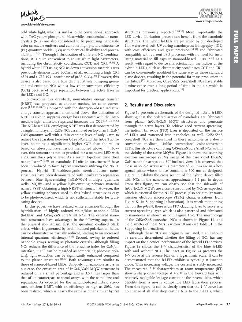
2. Results and Discussion
Figure 1 a presents a schematic of the designed hybrid h-LED, showing that the ordered arrays of nanoholes are fabricated from planar InGaN/GaN MQW structures and penetrate through the active layers. To achieve good current spreading, the indium tin oxide (ITO) layer is deposited on the surface of LEDs and patterned into nanoholes as well. CdSe/ZnS core/shell NCs are then fi lled in these nanoholes as a down-conversion medium. Unlike conventional color-conversion LEDs, this structure can bring CdSe/ZnS core/shell NCs within the vicinity of the active MQWs. Figure 1 b shows the scanning electron microscope (SEM) image of the bare violet InGaN/GaN nanohole arrays at a 30° inclined view. It is observed that these nanohole arrays with a diameter of 300 nm are in a hex-agonal lattice whose lattice constant is 600 nm as designed. Figure 1 c exhibits the cross section of the hybrid device fi lled with NCs in the nanoholes, approximately 1.2 µm in depth. From this fi gure, we can clearly see that the sidewalls of InGaN/GaN MQWs are closely surrounded by NCs as expected, which is essential for the NRET process (also see similar trans-mission electron microscope (TEM) characterizations from Figure S1 in Supporting Information). It is worth mentioning that on the p-GaN, there is an ITO cladding layer to serve as a current spreading layer, which is also patterned and fabricated to nanoholes as shown in both Figure 1 b,c. The morphology of the CdSe/ZnS core/shell NCs is shown in Figure 1 d, and the diameter of these NCs is within 10 nm (see Table S1 in the Supporting Information).
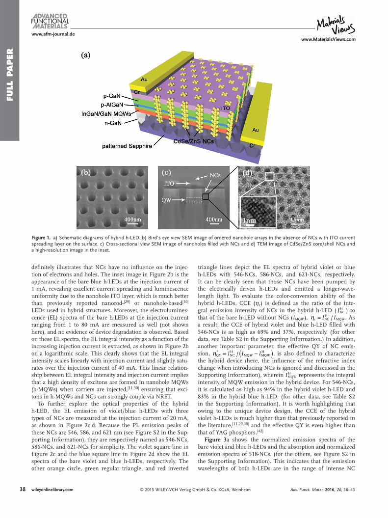
Although these NCs are originally insulated, it still should be carefully determined whether the fi lling of NCs has any impact on the electrical performance of the hybrid LED devices. Figure 2 a shows the I – V characteristics of the blue h-LED with and without NCs. The inset in Figure 2 a presents the I – V curve at the reverse bias on a logarithmic scale. It can be demonstrated that the h-LED exhibits a typical p–n junction diode. With increasing voltage, the current is stably increased. The measured I – V characteristics at room temperature (RT) show a sharp onset voltage at 4.5 V in the forward bias with relatively negligible leakage current at the reverse bias, which benefi ts from a mostly compatible LED fabrication process. From this fi gure, it can be clearly seen that the I – V curve has no change at all after drop casting NCs to the h-LEDs, which
Adv. Funct. Mater. 2016, 26, 36–43
www.afm-journal.dewww.MaterialsViews.com
FULL
PAPER
38 wileyonlinelibrary.com © 2015 WILEY-VCH Verlag GmbH & Co. KGaA, Weinheim
defi nitely illustrates that NCs have no infl uence on the injec-tion of electrons and holes. The inset image in Figure 2 b is the appearance of the bare blue h-LEDs at the injection current of 1 mA, revealing excellent current spreading and luminescence uniformity due to the nanohole ITO layer, which is much better than previously reported nanorod- [ 29 ] or nanohole-based [ 30 ] LEDs used in hybrid structures. Moreover, the electrolumines-cence (EL) spectra of the bare h-LEDs at the injection current ranging from 1 to 80 mA are measured as well (not shown here), and no evidence of device degradation is observed. Based on these EL spectra, the EL integral intensity as a function of the increasing injection current is extracted, as shown in Figure 2 b on a logarithmic scale. This clearly shows that the EL integral intensity scales linearly with injection current and slightly satu-rates over the injection current of 40 mA. This linear relation-ship between EL integral intensity and injection current implies that a high density of excitons are formed in nanohole MQWs (h-MQWs) when carriers are injected, [ 11,30 ] ensuring that exci-tons in h-MQWs and NCs can strongly couple via NRET.
To further explore the optical properties of the hybrid h-LED, the EL emission of violet/blue h-LEDs with three types of NCs are measured at the injection current of 20 mA, as shown in Figure 2 c,d. Because the PL emission peaks of these NCs are 546, 586, and 621 nm (see Figure S2 in the Sup-porting Information), they are respectively named as 546-NCs, 586-NCs, and 621-NCs for simplicity. The violet square line in Figure 2 c and the blue square line in Figure 2 d show the EL spectra of the bare violet and blue h-LEDs, respectively. The other orange circle, green regular triangle, and red inverted
triangle lines depict the EL spectra of hybrid violet or blue h-LEDs with 546-NCs, 586-NCs, and 621-NCs, respectively. It can be clearly seen that those NCs have been pumped by the electrically driven h-LEDs and emitted a longer-wave-length light. To evaluate the color-conversion ability of the hybrid h-LEDs, CCE ( η c ) is defi ned as the ratio of the inte-gral emission intensity of NCs in the hybrid h-LED ( NC
HI ) to that of the bare h-LED without NCs ( MQWI ), /c NC
HMQWI Iη = . As
a result, the CCE of hybrid violet and blue h-LED fi lled with 546-NCs is as high as 69% and 37%, respectively. (for other data, see Table S2 in the Supporting Information.) In addition, another important parameter, the effective QY of NC emis-sion, /QY
*NCH
MQW MQWHI I Iη ( )= − , is also defi ned to characterize
the hybrid device (here, the infl uence of the refractive index change when introducing NCs is ignored and discussed in the Supporting Information), wherein MQW
HI represents the integral intensity of MQW emission in the hybrid device. For 546-NCs, it is calculated as high as 94% in the hybrid violet h-LED and 83% in the hybrid blue h-LED. (for other data, see Table S2 in the Supporting Information). It is worth highlighting that owing to the unique device design, the CCE of the hybrid violet h-LEDs is much higher than that previously reported in the literature, [ 11,29,30 ] and the effective QY is even higher than that of YAG phosphors. [ 42 ]
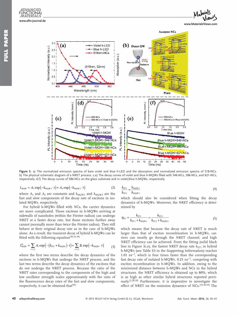
Figure 3 a shows the normalized emission spectra of the bare violet and blue h-LEDs and the absorption and normalized emission spectra of 518-NCs. (for the others, see Figure S2 in the Supporting Information). This indicates that the emission wavelengths of both h-LEDs are in the range of intense NC
Adv. Funct. Mater. 2016, 26, 36–43
www.afm-journal.dewww.MaterialsViews.com
Figure 1. a) Schematic diagrams of hybrid h-LED. b) Bird’s eye view SEM image of ordered nanohole arrays in the absence of NCs with ITO current spreading layer on the surface. c) Cross-sectional view SEM image of nanoholes fi lled with NCs and d) TEM image of CdSe/ZnS core/shell NCs and a high-resolution image in the inset.

FULL P
APER
39wileyonlinelibrary.com© 2015 WILEY-VCH Verlag GmbH & Co. KGaA, Weinheim
absorption, indicating good spectral overlaps of MQWs with the NC absorption and guaranteeing strong coupling between the excitons in MQWs and the absorption dipoles of NCs at the specifi c wavelength. Figure 3 b displays the physical diagram of the NRET process between the InGaN/GaN MQWs and the NCs along with the relaxation process in the hybrid struc-tures. As a result of the geometry, the coupling actually occurs between the excitons in MQWs (dot) and a 2D-like assembly of NCs (plane), which in fact act as a 1D confi ned structure. [ 1,22 ] As shown, by optical pumping or current injection, carriers are generated, and excitons are distributed in MQWs. These excitons can recombine either radiatively to emit photons or nonradiatively by defects or experience resonant NRET into an assembly of NCs if the excitonic energy of MQWs can match the absorption energy of NCs. After the energy is transferred to NCs, an extremely fast intraband relaxation in NCs will happen at once, removing excitons from resonance with the MQW transition and effectively preventing the back-transfer process. [ 1 ] The relaxed excitons in the NCs then primarily recombine radiatively, emitting photons with an energy corresponding to the NC’s bandgap. In this geometry, the decay rate of NRET is described as [ 28,43 ]
2
ET MQWNC 0
6
4 MQW0
4
k kR
dk
R
d
βπσ= = ′⎛⎝⎜
⎞⎠⎟ (1)
where k MQW is the de-excitation rate of the MQW excited state in the absence of NCs, σ NC is the NC’s surface density, R 0 and R 0 ′ are the point-to-point and modifi ed Förster radii,
respectively, here radius is defi ned as the separation distance between donors and acceptors when the NRET effi ciency becomes equal to 50%; d is the separation between the exci-tons in the MQWs and NCs; and β is the modifi ed factor. A detailed derivation of Equation ( 1) is included in the Sup-porting Information.
To explore the carrier dynamics and reveal the NRET pro-cess, the RT temporal evolution of PL in hybrid violet/blue h-MQWs, as well as isolated h-MQWs and NCs, is monitored, as shown in Figure 3 c,e. (see Figure S3 in the Supporting Information.) All recorded PL signals correspond to the peak emission wavelength of h-MQWs or NCs. It can be seen that the excitons in both hybrid h-MQWs decay signifi cantly faster (approximately four times faster, according to the fi ts discussed later) compared with their isolated counterparts, accounting for an existing NRET process that introduces an additional decay channel for the excitons in the hybrid h-MQWs, as explained in Figure 3 b. It is worth mentioning that similar time-resolved photoluminescence (TRPL) measurements are performed on blue h-MQWs coated with an organic material (polymethyl methacrylate, PMMA), which has no absorption at the InGaN/GaN MQW emission wavelength. (see Figure S5 in the Sup-porting Information). It is found that there is no change in the decay lifetime of blue h-MQWs coated with PMMA compared with bare h-MQWs, further confi rming that the decay change of hybrid h-MQWs is due to the NRET process instead of the change in the refractive index of nanoholes.
For isolated h-MQWs, the decay curves can be simply fi tted with a double exponential decay as follows [ 2,31,34 ]
Adv. Funct. Mater. 2016, 26, 36–43
www.afm-journal.dewww.MaterialsViews.com
Figure 2. a) I – V characteristics of the h-LEDs with and without NCs. The inset is the I – V curve at the reverse bias on a logarithmic scale. b) The trend of the EL integral intensity as a function of the injection current. The inset is a CCD image of the bare blue h-LEDs at the injection current of 1 mA. The EL spectra of the hybrid c) violet and d) blue h-LEDs fi lled with 546-NCs, 586-NCs, and 621-NCs at the injection current of 20 mA, respectively.
FULL
PAPER
40 wileyonlinelibrary.com © 2015 WILEY-VCH Verlag GmbH & Co. KGaA, Weinheim
exp expMQW 1 MQW1 2 MQW2I A k t A k t( ) ( )= − ⋅ + − ⋅ (2)
where A 1 and A 2 are constants and k MQW1 and k MQW2 are the fast and slow components of the decay rate of excitons in iso-lated MQWs, respectively.
For hybrid h-MQWs fi lled with NCs, the carrier dynamics are more complicated. Those excitons in h-MQWs arriving at sidewalls of nanoholes (within the Förster radius) can undergo NRET at a faster decay rate, but those excitons further away cannot (normally more than twice the Förster radius). They still behave at their original decay rate as in the case of h-MQWs alone. As a result, the transient decay of hybrid h-MQWs can be fi tted with the following equation [ 30,31,44 ]
exp expMQWH
ET MQW1,2
MQW1,2
I A k k t B k ti i i
i
i i
i∑ ∑( )( ) ( )= − + ⋅ + − ⋅= =
(3)
where the fi rst two terms describe the decay dynamics of the excitons in h-MQWs that undergo the NRET process, and the last two terms describe the decay dynamics of the excitons that do not undergo the NRET process. Because the ratio of the NRET rates corresponding to the components of the high and low oscillator strength scales approximately with the ratio of the fl uorescence decay rates of the fast and slow components, respectively, it can be obtained that [ 44 ]
ET1
ET2
MQW1
MQW2
k
k
k
k= (4)
which should also be considered when fi tting the decay dynamics of h-MQWs. Moreover, the NRET effi ciency is deter-mined by
ETET1
ET1 MQW1
ET2
ET2 MQW2
k
k k
k
k kη =
+=
+ (5)
which means that because the decay rate of NRET is much larger than that of exciton recombination in h-MQWs, car-riers can mostly go through the NRET channel, and high NRET effi ciency can be achieved. From the fi tting (solid black line in Figure 3 c,e), the fastest NRET decay rate k ET1 in hybrid h-MQWs (see Table S3 in the Supporting Information) reaches 1.01 ns −1 , which is four times faster than the corresponding fast decay rate of isolated h-MQWs, 0.25 ns −1 , competing with exciton recombination in h-MQWs. In addition, owing to the minimized distance between h-MQWs and NCs in the hybrid structures, the NRET effi ciency is obtained up to 80%, which is as high as other similar hybrid structures reported previ-ously. [ 2,28,30 ] Furthermore, it is imperative to investigate the effect of NRET on the emission dynamics of NCs. [ 10,30,44 ] The
Adv. Funct. Mater. 2016, 26, 36–43
www.afm-journal.dewww.MaterialsViews.com
Figure 3. a) The normalized emission spectra of bare violet and blue h-LED and the absorption and normalized emission spectra of 518-NCs. b) The physical schematic diagram of a NRET process. c,e) The decay curves of violet and blue h-MQWs fi lled with 546-NCs, 586-NCs, and 621-NCs, respectively. d,f) The decay curves of 586-NCs on the glass substrate and in violet/blue h-MQWs, respectively.

FULL P
APER
41wileyonlinelibrary.com© 2015 WILEY-VCH Verlag GmbH & Co. KGaA, Weinheim
insets in Figure 3 d and f show the rising time of the transient fl uorescence decays of 586-NCs on the glass substrate and in violet/blue h-MQWs, respectively, which defi nitely demonstrate the slowing rising time of NCs in violet/blue h-MQWs com-pared with that of the isolated ones. Moreover, the fl uorescence decays of 586-NCs in violet/blue h-MQWs reveal good agree-ment with the fi tted curves (see Figure S6 in the Supporting Information), unequivocally proving that NRET exists in the hybrid h-LEDs studied here.
It is known that the NRET process mainly depends on the coupling distance d between the MQWs and NCs. [ 45 ] By utilizing Equation ( 1) , the average coupling distance d of NRET in the hybrid structures ranges from 5.2 to 7.7 nm, which is smaller than the modifi ed Förster’s radius R 0 ′ (see Table S4 in the Supporting Information), implying that the coupling between h-MQWs and NCs is strong enough to achieve a high effi ciency of NRET. Moreover, it is noticed that the average coupling dis-tance d is also smaller than a single NC diameter, illustrating that except for the fi rst layer of NCs attached to the sidewalls of h-MQWs, the NCs further away may not undergo NRET. As a result, the nanohole arrays with an emission area 3.5 times larger can have equivalent NRET coupling compared with the nanorod arrays due to the equal area of their sidewalls, which exhibits an advantage of the nanohole-based hybrid structures.
With regard to high-quality hybrid white LEDs, it is impor-tant to modify the optical parameters such as the chromaticity coordinates, CCT, and CRI. First, a mathematical model is
adopted [ 46 ] to simulate violet and blue h-LEDs with different color schemes. The spectral power distributions of hybrid violet/blue h-LEDs are given by (see the Supporting Information)
white MQW NC1 NC1 NC2 NC2S S k S k Sλ λ λ λ( ) ( ) ( ) ( )= + ⋅ + ⋅ +� (6)
where k NC1 , k NC2 … are the ratios of the peak intensity of NCs to those of LEDs.
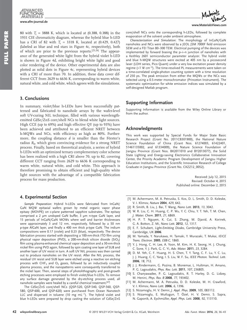
Because the CRI of the binary complementary color scheme (h-LEDs + one type of NCs) is low (see Figure S7 in the Supporting Information), hybrid h-LEDs with ter-nary complementary color (h-LEDs + two types of NCs) are considered. Figure 4 a shows the simulated results plotted in the 1931 CIE chromaticity diagram, the chromaticity coordi-nates of which approach the blackbody line. Four schemes pre-sent good performance among all types of schemes between h-LEDs and NCs, as labeled in Figure 4 a. The CRI has arrived at 70–80 and 75–86 for hybrid violet and blue h-LEDs, respec-tively. Moreover, these points are across CCT areas from 2500 to 10 000 K, revealing that the hybrid h-LEDs can be accessed to change the CCT for various applications. Based on this simula-tion, two schemes, hybrid violet h-LEDs + 518-NCs + 600-NCs and blue h-LEDs + 546-NCs + 621-NCs, are adopted for experi-ments and labelled with stars in Figure 4 a. Figure 4 b exhibits the EL spectra of the two combinations of hybrid devices normalized to the peak intensity of h-LED emission at the injec-tion current of 20 mA. The hybrid violet h-LED has a CRI of
Adv. Funct. Mater. 2016, 26, 36–43
www.afm-journal.dewww.MaterialsViews.com
Figure 4. a) Simulated CIE 1931 chromaticity diagram of ternary complementary color hybrid h-LEDs. b) The EL spectra of hybrid violet and blue LEDs with a CRI of 80 and 82, respectively. c) The experiment data locations in the CIE 1931 chromaticity diagram of ternary complementary color hybrid h-LEDs marked with stars in (a). d) The picture of the generated white light of hybrid violet h-LED at the injection current of 20 mA.
FULL
PAPER
42 wileyonlinelibrary.com © 2015 WILEY-VCH Verlag GmbH & Co. KGaA, Weinheim Adv. Funct. Mater. 2016, 26, 36–43
www.afm-journal.dewww.MaterialsViews.com
80 with T c = 3888 K, which is located at (0.388, 0.388) in the 1931 CIE chromaticity diagram, whereas the hybrid blue h-LED has a CRI of 82 with T c = 3318 K, located at (0.429, 0.427) (labeled as blue and red stars in Figure 4 c, respectively), both of which are prior to the previous reports. [ 25,26 ] The appear-ance of the generated white light from the hybrid violet h-LED is shown in Figure 4 d, exhibiting bright white light and good color rendering of the device. Other experimental data are also plotted as solid dots in Figure 4 c, representing hybrid devices with a CRI of more than 70. In addition, these data cover dif-ferent CCT from 2629 to 6636 K, corresponding to warm white, natural white, and cold white, which agrees with the simulations.
3. Conclusions
In summary, violet/blue h-LEDs have been successfully pat-terned and fabricated to nanohole arrays by the wafer-level soft UV-curing NIL technique, fi lled with various wavelength-emitted CdSe/ZnS core/shell NCs to blend white light sources. High CCE (up to 69%) and high effective QY (up to 93%) have been achieved and attributed to an effi cient NRET between h-MQWs and NCs, with effi ciency as high as 80%. Further-more, the coupling distance d is smaller than the Förster’s radius R 0 , which gives convincing evidence for a strong NRET process. Finally, based on theoretical analysis, a series of hybrid h-LEDs with an optimized ternary complementary color scheme has been realized with a high CRI above 70, up to 82, covering different CCT ranging from 2629 to 6636 K corresponding to warm white, natural white, and cold white. This approach is therefore promising to obtain effi cient and high-quality white light sources with the advantage of a compatible fabrication process for mass production.
4. Experimental Section Sample Preparation : Hybrid h-LEDs were fabricated from InGaN/
GaN MQW epitaxial wafers grown by metal organic vapor phase epitaxy (MOVPE) on c-plane patterned sapphire substrates. The epitaxy comprised a 2 µm undoped GaN buffer, 3 µm n-type GaN layer, and 15 periods of InGaN/GaN MOWs where well and barrier thicknesses were approximately 3 and 12 nm, respectively, followed by a 50 nm p-type AlGaN layer, and fi nally a 400 nm thick p-type GaN. The indium compositions were 0.17 (violet) and 0.23 (blue), respectively. The device fabrication process started with depositing a 100-nm-thick ITO fi lm using physical vapor deposition (PVD), a 200-nm-thick silicon dioxide (SiO 2 ) fi lm using plasma-enhanced chemical vapor deposition and a 30-nm-thick nickel fi lm using PVD again, followed by spin coating one layer of SU8 and another layer of UV resist in turn. A soft UV NIL process was then carried out to produce nanoholes on the UV resist. After the NIL process, the residual UV resist and SU8 layer were etched using a reactive ion etching process with CHF 3 and O 2 gases, followed by an inductively coupled plasma process, and the nanopatterns were consequently transferred to the nickel layer. Then, several steps of photolithography and post-growth etching processes were employed to fi nish violet/blue h-LEDs. To remove any surface damage generated by the dry-etching process used, all nanohole samples were healed by a careful chemical treatment. [ 47 ]
The CdSe/ZnS core/shell NCs (QSP-520, QSP-540, QSP-560, QSP-580, QSP-600, and QSP-620) were purchased from Ocean Nanotech LLC and dispersed in toluene (10 mg mL −1 ). The hybrid violet and blue h-LEDs were prepared by drop casting the solution of CdSe/ZnS
core/shell NCs onto the corresponding h-LEDs, followed by complete evaporation of the solvent under ambient atmosphere.
Characterization and Simulation : The morphology of InGaN/GaN nanoholes and NCs were observed by a JEOL JSM 7000F fi eld emission SEM and a FEI Titan 80–300 TEM. Electrical pumping of the devices was implemented by forward biasing the p–i–n junction of nanoholes with a Keithley 2601 semiconductor parameter analyzer. The hybrid violet and blue h-MQW structures were excited at 405 nm by a picosecond laser (LDH series, Pico Quant) under a very low excitation power density regime (≈1 W cm −2 ). The time-resolved PL measurements were taken on a time-correlated single-photon counting system with a time resolution of 250 ps. The peak emission from either the MQWs or the NCs was selected using a 0.5-meter monochromator (Princeton Instrument). The systematic optimization for white emission indices was simulated by a self-designed Matlab program.
Supporting Information Supporting Information is available from the Wiley Online Library or from the author.
Acknowledgments This work was supported by Special Funds for Major State Basic Research Project (Grant No. 2011CB301900), the National Nature Science Foundation of China (Grant Nos. 61274003, 61422401, 51461135002, and 61334009), the Nature Science Foundation of Jiangsu Province (Grant Nos. BK2011010 and BY2013077), the Solid State Lighting and Energy-saving Electronics Collaborative Innovation Center, the Priority Academic Program Development of Jiangsu Higher Education Institutions, and the Scientifi c Innovation Research of College Graduate in Jiangsu Province (Grant No. CXZZ12_0052).
Received: July 12, 2015 Revised: October 4, 2015
Published online: December 2, 2015
[1] M. Achermann , M. A. Petruska , S. Kos , D. L. Smith , D. D. Koleske , V. I. Klimov , Nature 2004 , 429 , 642 .
[2] R. Smith , B. Liu , J. Bai , T. Wang , Nano Lett. 2013 , 13 , 3042 . [3] W. R. Liu , C. H. Huang , C. P. Wu , Y. C. Chiu , Y. T. Yeh , T. M. Chen ,
J. Mater. Chem. 2011 , 21 , 6869 . [4] H. P. T. Nguyen , K. Cui , S. Zhang , M. Djavid , A. Korinek ,
G. A. Botton , Z. Mi , Nano Lett. 2012 , 12 , 1317 . [5] E. F. Schubert , Light-Emitting Diodes , Cambridge University Press ,
Cambridge, UK 2006 . [6] M. Yamada , Y. Narukawa , H. Tamaki , Y. Murazaki , T. Mukai , IEICE
Trans. Electron. 2005 , E88-C , 1860 . [7] Y. J. Hong , C. H. Lee , A. Yoon , M. Kim , H. K. Seong , H. J. Chung ,
C. Sone , Y. J. Park , G. C. Yi , Adv. Mater. 2011 , 23 , 3284 . [8] D. M. Yeh , C. F. Huang , H. S. Chen , T. Y. Tang , C. F. Lu , Y. C. Lu ,
J. J. Huang , C. C. Yang , I. S. Liu , W. F. Su , IEEE Photon. Technol. Lett. 2006 , 18 , 712 .
[9] J. J. Rindermann , G. Pozina , B. Monemar , L. Hultman , H. Amano , P. G. Lagoudakis , Phys. Rev. Lett. 2011 , 107 , 236805.
[10] S. Chanyawadee , P. G. Lagoudakis , R. T. Harley , D. G. Lidzey , M. Henini , Phys. Rev. B 2008 , 77 , 193402 .
[11] M. Achermann , M. A. Petruska , D. D. Koleske , M. H. Crawford , V. I. Klimov , Nano Lett. 2006 , 6 , 1396 .
[12] S. Nizamoglu , H. V. Demir , J. Appl. Phys. 2009 , 105 , 083112. [13] S. Nizamoglu , E. Mutlugun , T. Özel , H. V. Demir , S. Sapra ,
N. Gaponik , A. Eychmüller , Appl. Phys. Lett. 2008 , 92 , 113110 .
FULL P
APER
43wileyonlinelibrary.com© 2015 WILEY-VCH Verlag GmbH & Co. KGaA, WeinheimAdv. Funct. Mater. 2016, 26, 36–43
www.afm-journal.dewww.MaterialsViews.com
[14] S. Nizamoglu , G. Zengin , H. V. Demir , Appl. Phys. Lett. 2008 , 92 , 031102 .
[15] E. Jang , S. Jun , H. Jang , J. Llim , B. Kim , Y. Kim , Adv. Mater. 2010 , 22 , 3076 .
[16] N. J. Findlay , J. Bruckbauer , A. R. Inigo , B. Breig , S. Arumugam , D. J. Wallis , R. W. Martin , P. J. Skabara , Adv. Mater. 2014 , 26 , 7290 .
[17] D. V. Talapin , J. Steckel , MRS Bull. 2013 , 38 , 685 . [18] W. K. Bae , S. Brovelli , V. I. Klimov , MRS Bull. 2013 , 38 , 721 . [19] T. Erdem , H. V. Demir , Nanophotonics 2013 , 2 , 57 . [20] Q. Dai , C. E. Duty , M. Z. Hu , Small 2010 , 6 , 1577 . [21] H. V. Demir , S. Nizamoglu , T. Erdem , E. Mutlugun , N. Gaponik ,
A. Eychmueller , Nano Today 2011 , 6 , 632 . [22] B. Guzelturk , P. L. H. Martinez , Q. Zhang , Q. Xiong , H. Sun ,
X. W. Sun , A. O. Govorov , H. V. Demir , Laser Photonics Rev. 2014 , 8 , 73 . [23] K. Kim , J. Y. Woo , S. Jeong , C. S. Han , Adv. Mater. 2011 , 23 , 911 . [24] S. Bhaviripudi , J. Qi , E. L. Hu , A. M. Belcher , Nano Lett. 2007 , 7 ,
3512 . [25] S. Nizamoglu , T. Ozel , E. Sari , H. V. Demir , Nanotechnology 2007 ,
18 , 065709 . [26] C. Dang , J. Lee , Y. Zhang , J. Han , C. Breen , J. S. Steckel , C. S. Seth ,
A. Nurmikko , Adv. Mater. 2012 , 24 , 5915 . [27] H. S. Chen , C. K. Hsu , H. Y. Hong , IEEE Photon. Technol. Lett. 2006 ,
18 , 193 . [28] B. Guzelturk , S. Nizamoglu , D. W. Jeon , I. H. Lee , H. V. Demir ,
presented at Conference on Lasers and Electro-Optics 2012 , New York , May 2012 .
[29] F. Zhang , J. Liu , G. You , C. Zhang , S. E. Mohney , M. J. Park , J. S. Kwak , Y. Wang , D. D. Koleske , J. Xu , Opt. Express 2012 , 20 , A333 .
[30] S. Chanyawadee , P. G. Lagoudakis , R. T. Harley , M. D. B. Charlton , D. V. Talapin , H. W. Huang , C. H. Lin , Adv. Mater. 2010 , 22 , 602 .
[31] S. Nizamoglu , B. Guzelturk , D. W. Jeon , I. H. Lee , H. V. Demir , Appl. Phys. Lett. 2011 , 98 , 163108 .
[32] S. Nizamoglu , H. V. Demir , Appl. Phys. Lett. 2009 , 95 , 151111 . [33] B. Jiang , C. Zhang , X. Wang , M. J. Park , J. S. Kwak , J. Xu , H. Zhang ,
J. Zhang , F. Xue , M. Xiao , Adv. Funct. Mater. 2012 , 22 , 3146 . [34] B. Liu , R. Smith , J. Bai , Y. Gong , T. Wang , Appl. Phys. Lett. 2013 , 103 ,
101108 . [35] Q. Wang , J. Bai , Y. P. Gong , T. Wang , J. Phys. D, Appl. Phys. 2011 ,
44 , 395102 . [36] M. Athanasiou , T. K. Kim , B. Liu , R. Smith , T. Wang , Appl. Phys. Lett.
2013 , 102 , 191108 . [37] K. McGroddy , A. David , E. Matioli , M. Iza , S. Nakamura ,
S. DenBaars , J. S. Speck , C. Weisbuch , E. L. Hu , Appl. Phys. Lett. 2008 , 93 , 103502 .
[38] X. Guo , J. Hu , Z. Zhuang , M. Deng , F. Wu , X. Li , B. Liu , C. Yuan , H. Ge , F. Li , Y. Chen , J. Vac. Sci. Technol. B 2014 , 32 , 06FG06.
[39] Z. Zhuang , X. Guo , G. Zhang , B. Liu , R. Zhang , T. Zhi , T. Tao , H. Ge , F. Ren , Z. Xie , Y. Zheng , Nanotechnology 2013 , 24 , 405303 .
[40] L. Y. Chen , Y. Y. Huang , C. H. Chang , Y. H. Sun , Y. W. Cheng , M. Y. Ke , C. P. Chen , J. Huang , Opt. Express 2010 , 18 , 7664 .
[41] R. Xie , U. Kolb , J. Li , T. Basché , A. Mews , J. Am. Chem. Soc. 2005 , 127 , 7480 .
[42] S. C. Allen , A. J. Steckl , Appl. Phys. Lett. 2008 , 92 , 143309 . [43] J. R. Lakowicz , Principles of Fluorescence Spectroscopy , Springer ,
New York 2006 . [44] S. Chanyawadee , R. T. Harley , M. Henini , D. V. Talapin , P. G. Lagoudakis ,
Phys. Rev. Lett. 2009 , 102 , 077402 . [45] S. Rohrmoser , J. Baldauf , R. T. Harley , P. G. Lagoudakis , S. Sapra ,
A. Eychmüller , I. M. Watson , Appl. Phys. Lett. 2007 , 91 , 092126 . [46] Y. Ohno , Opt. Eng. 2005 , 44 , 111302 . [47] Y. D. Zhuang , C. J. Lewins , S. Lis , P. A. Shields , D. W. E. Allsopp ,
IEEE Photon. Technol. Lett. 2013 , 25 , 1047 .