Embed Size (px)
Citation preview
INSTITUTE OF AERONAUTICAL ENGINEERING (Autonomous)
Dundigal, Hyderabad - 500 043
ELECTRICAL AND ELECTRONICS ENGINEERING
QUESTION BANK
Course Title ELECTRONIC CIRCUITS
Course Code A40413
Regulation R15
Course Structure Lectures Tutorials Practicals Credits
4 -- -- 4
Course Coordinator Ms Anusha. N , Assistant Professor
Team of Instructors Ms Anusha. N, Assistant Professor
OBJECTIVES
To meet the challenge of ensuring excellence in engineering education, the issue of quality needs to be
addressed, debated and taken forward in a systematic manner. Accreditation is the principal means of quality
assurance in higher education. The major emphasis of accreditation process is to measure the outcomes of the
program that is being accredited.
In line with this, Faculty of Institute of Aeronautical Engineering, Hyderabad has taken a lead in incorporating
philosophy of outcome based education in the process of problem solving and career development. So, all
students of the institute should understand the depth and approach of course to be taught through this question
bank, which will enhance learner‟s learning process.
1. GROUP - A (SHORT ANSWER QUESTIONS)
S.NO
QUESTION
BLOOMS
TAXONOMY
LEVEL
COURSE
OUTCOMES
UNIT - I
SINGLE STAGE AMPLIFIERS DESIGN AND ANALYSIS
1 Define an Amplifier? Remembering 1
2 Describe the single stage amplifier? Remembering 1
3 Write the advantages of CE configuration over CB and CC configurations? Applying 1
4 Classify the amplifiers based on different parameters? Understanding 1
5 Distinguish among three configurations? Understanding 1
6 Write the advantages of FET over BJT? Applying 2
7 Arrange the hybrid equivalent model of a CE amplifier? Remembering 1
8 Discuss a small signal JFET model of a common drain amplifier. Understanding 2
9 Define various hybrid parameters of a Transistor? Remembering 1
10 List out the characteristics of Common Emitter amplifier? Remembering 7
11 Explain the small signal model for common source amplifier? Understanding 7
12 Write the advantages of Emitter follower? Applying 7
13 List the benefits of H- Parameters? Remembering 1
14 Name the typical values of h-parameters for a transistor in CE, CB, CC
configurations?
Remembering 1
S.NO
QUESTION
BLOOMS
TAXONOMY
LEVEL
COURSE
OUTCOMES
15 Explain the typical frequency response of an RC coupled amplifier Understanding 1
16 Justify why the common emitter amplifier provides 180° phase shift
between input and output?
Evaluating 1
17 Construct the approximate h-parameter model for CE amplifier? Creating 1
19 Define a distortion in amplifiers? Give the classification of distortion? Remembering 1
20 Define amplitude distortion? Remembering 1
21 Define frequency distortion? Remembering 1
22 Define phase or Delay distortion? Remembering 1
23 Justify the statement, Why the amplitude distortion is called as harmonic
distortion?
Evaluating 1
24 Analyze the components affecting the frequency response of RC coupled
amplifier at low frequencies?
Analyzing 1
25 Justify the answer, why frequency response of RC coupled amplifier
decreases at high frequencies?
Evaluating 1
26 Define the concept of feedback in amplifiers? Remembering 4
27 Discuss the types of feedback? Understanding 4
28 Classify the feedback amplifiers based on the type of mixing and type of
sampling?
Understanding 4
29 Write the advantages of negative feedback? Applying 4
30 Distinguish the negative feedback and positive feedback? Analyzing 4
31 Discuss how does negative feedback reduce distortion in an amplifier? Understanding 4
32 Define sensitivity of an amplifier? Remembering 1
33 Analyze the effect of negative feedback on bandwidth? Analyzing 4
34 Calculate new gain, if An amplifier with stage gain 200 is provided with
negative feedback of feedback ratio 0.05.
Analyzing 4
35 Write the relation between lower cut off frequencies with and without
feedback.
Applying 4
37 Calculate the feedback ratio, if An amplifier has a gain of 300. When
negative feedback is applied, the gain is reduced to 240.
Analyzing 4
38 Estimate the input impedance of the feedback amplifier? If An amplifier
with Zi = 2KΩ has a voltage gain A = 200. If a negative feedback of β =
0.01 is applied to it.
Evaluating 4
39 Calculate the feedback factor. Express the amount of negative feedback in
dB. If the gain of an amplifier is decreased to 10,000 with negative
feedback from its gain of 60,000.
Analyzing 4
40 Define an oscillator? Remembering 4
UNIT-II
BJT AND FREQUENCY RESPONSE
1 Explain the significance of logarithmic scale? Understanding 3
2 Define “bel” and “Decibel”?. Remembering 3
3 Discuss the half bandwidth calculation of a transistor? Understanding 3
4 Define dBs? Remembering 3
5 Define half power frequencies? Remembering 3
6 Discuss the effect of emitter bypass capacitor on low frequency response
of BJT amplifiers.
Understanding 3
7 Sketch the high frequency π model of a transistor and explain in brief. Applying 3
8 Define fα and fβ cut-off frequencies in Hybrid-π model. Remembering 3
S.NO
QUESTION
BLOOMS
TAXONOMY
LEVEL
COURSE
OUTCOMES
9 Define square wave testing? What is need for it? Remembering 3
10 Define fT? Remembering 3
11 Discuss the effect of coupling capacitors on low frequency response of
BJT amplifiers.
Understanding 3
12 Write short notes on miller‟s theorem. Creating 3
13 Evaluate the relationship between low frequency h-parameters and high
frequency parameters.
Evaluating 3
14 Describe how internal capacitances affect the gain of BJT amplifier. Evaluating 3
15 Define Band width of an amplifier? Remembering 3
16 Define gain-bandwidth product? Remembering 3
17 Define unity-gain frequency? Remembering
18 Define voltage gain of the amplifier at fT? Remembering 3
19 Discuss the internal BJT capacitances and explain their effects. Understanding 3
20 Express power gain in dB Understanding 3
21 Express voltage gain in dB. Understanding 3
22 Evaluate the mid-range voltage gain of a transistor? Evaluating 3
23 Sketch a small signal JFET model of a common drain amplifier. Applying 3
24 Sketch a voltage divider bias FET network. Applying 3
25 Write the relationship between the hie and rbb‟. Creating 3
UNIT-III
MULTIVIBRATORS, CLIPPERS AND CLAMPERS
1 Define a multivibrator? How many states does it have. Remembering 2
2 Describe a bistable multivibrator? Understanding 2
3 Classify the multivibrators?. Understanding 2
4 Indicate the other names of a bistable multivibrator? Understanding 2
5 Describe the bistable multivibrator. Understanding 2
6 Define an ac coupling in multivibrators? Remembering 2
7 Name the applications of a bistable multivibrator? Remembering 2
8 Define stable state of a binary? Remembering 2
9 Define quasi-stable state? Remembering 2
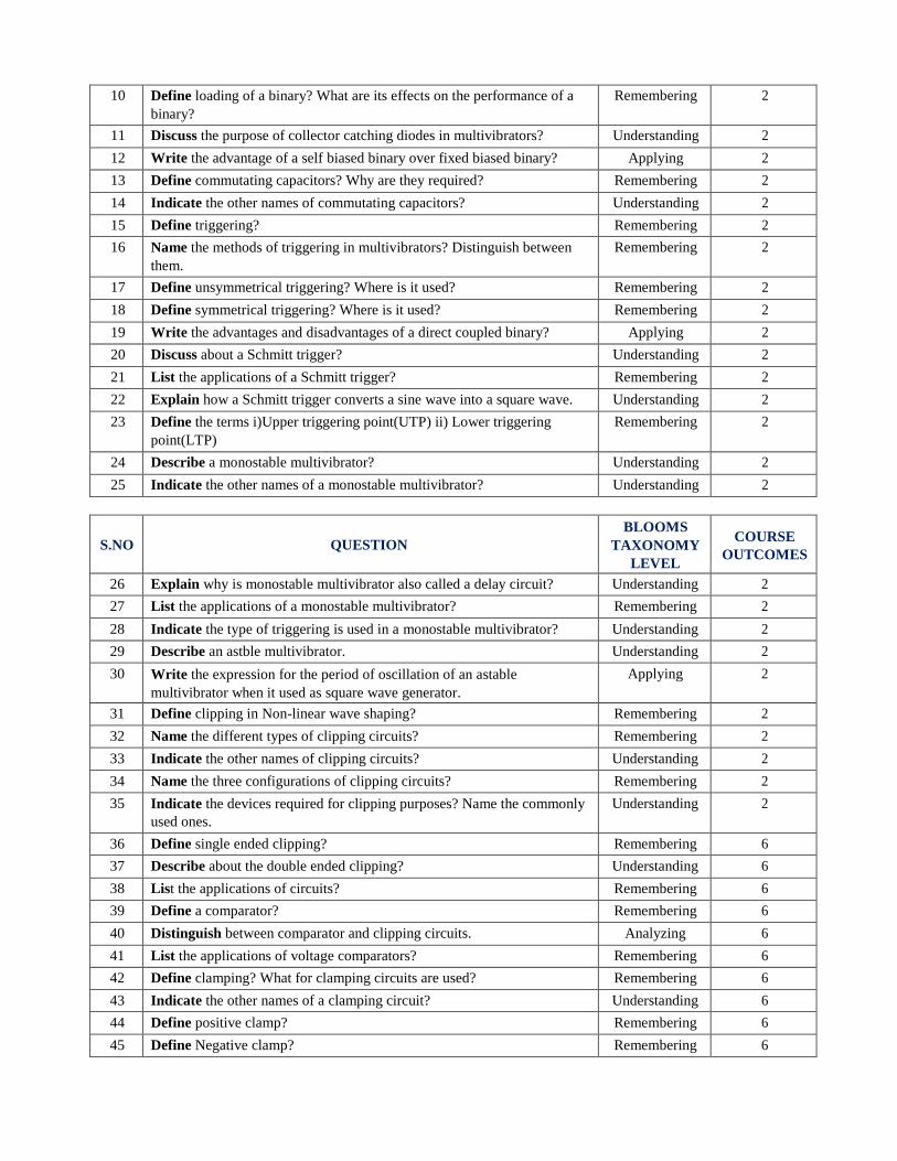
10 Define loading of a binary? What are its effects on the performance of a
binary?
Remembering 2
11 Discuss the purpose of collector catching diodes in multivibrators? Understanding 2
12 Write the advantage of a self biased binary over fixed biased binary? Applying 2
13 Define commutating capacitors? Why are they required? Remembering 2
14 Indicate the other names of commutating capacitors? Understanding 2
15 Define triggering? Remembering 2
16 Name the methods of triggering in multivibrators? Distinguish between
them.
Remembering 2
17 Define unsymmetrical triggering? Where is it used? Remembering 2
18 Define symmetrical triggering? Where is it used? Remembering 2
19 Write the advantages and disadvantages of a direct coupled binary? Applying 2
20 Discuss about a Schmitt trigger? Understanding 2
21 List the applications of a Schmitt trigger? Remembering 2
22 Explain how a Schmitt trigger converts a sine wave into a square wave. Understanding 2
23 Define the terms i)Upper triggering point(UTP) ii) Lower triggering
point(LTP)
Remembering 2
24 Describe a monostable multivibrator? Understanding 2
25 Indicate the other names of a monostable multivibrator? Understanding 2
S.NO
QUESTION
BLOOMS
TAXONOMY
LEVEL
COURSE
OUTCOMES
26 Explain why is monostable multivibrator also called a delay circuit? Understanding 2
27 List the applications of a monostable multivibrator? Remembering 2
28 Indicate the type of triggering is used in a monostable multivibrator? Understanding 2
29 Describe an astble multivibrator. Understanding 2
30 Write the expression for the period of oscillation of an astable
multivibrator when it used as square wave generator.
Applying 2
31 Define clipping in Non-linear wave shaping? Remembering 2
32 Name the different types of clipping circuits? Remembering 2
33 Indicate the other names of clipping circuits? Understanding 2
34 Name the three configurations of clipping circuits? Remembering 2
35 Indicate the devices required for clipping purposes? Name the commonly
used ones.
Understanding 2
36 Define single ended clipping? Remembering 6
37 Describe about the double ended clipping? Understanding 6
38 List the applications of circuits? Remembering 6
39 Define a comparator? Remembering 6
40 Distinguish between comparator and clipping circuits. Analyzing 6
41 List the applications of voltage comparators? Remembering 6
42 Define clamping? What for clamping circuits are used? Remembering 6
43 Indicate the other names of a clamping circuit? Understanding 6
44 Define positive clamp? Remembering 6
45 Define Negative clamp? Remembering 6
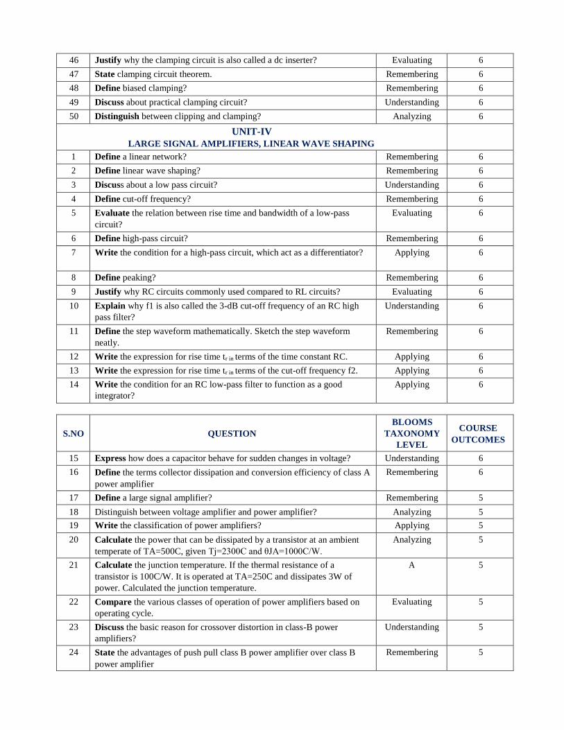
46 Justify why the clamping circuit is also called a dc inserter? Evaluating 6
47 State clamping circuit theorem. Remembering 6
48 Define biased clamping? Remembering 6
49 Discuss about practical clamping circuit? Understanding 6
50 Distinguish between clipping and clamping? Analyzing 6
UNIT-IV
LARGE SIGNAL AMPLIFIERS, LINEAR WAVE SHAPING
1 Define a linear network? Remembering 6
2 Define linear wave shaping? Remembering 6
3 Discuss about a low pass circuit? Understanding 6
4 Define cut-off frequency? Remembering 6
5 Evaluate the relation between rise time and bandwidth of a low-pass
circuit?
Evaluating 6
6 Define high-pass circuit? Remembering 6
7 Write the condition for a high-pass circuit, which act as a differentiator? Applying 6
8 Define peaking? Remembering 6
9 Justify why RC circuits commonly used compared to RL circuits? Evaluating 6
10 Explain why f1 is also called the 3-dB cut-off frequency of an RC high
pass filter?
Understanding 6
11 Define the step waveform mathematically. Sketch the step waveform
neatly.
Remembering 6
12 Write the expression for rise time tr in terms of the time constant RC. Applying 6
13 Write the expression for rise time tr in terms of the cut-off frequency f2. Applying 6
14 Write the condition for an RC low-pass filter to function as a good
integrator?
Applying 6
S.NO
QUESTION
BLOOMS
TAXONOMY
LEVEL
COURSE
OUTCOMES
15 Express how does a capacitor behave for sudden changes in voltage? Understanding 6
16 Define the terms collector dissipation and conversion efficiency of class A
power amplifier
Remembering 6
17 Define a large signal amplifier? Remembering 5
18 Distinguish between voltage amplifier and power amplifier? Analyzing 5
19 Write the classification of power amplifiers? Applying 5
20 Calculate the power that can be dissipated by a transistor at an ambient
temperate of TA=500C, given Tj=2300C and θJA=1000C/W.
Analyzing 5
21 Calculate the junction temperature. If the thermal resistance of a
transistor is 100C/W. It is operated at TA=250C and dissipates 3W of
power. Calculated the junction temperature.
A 5
22 Compare the various classes of operation of power amplifiers based on
operating cycle.
Evaluating 5
23 Discuss the basic reason for crossover distortion in class-B power
amplifiers?
Understanding 5
24 State the advantages of push pull class B power amplifier over class B
power amplifier
Remembering 5
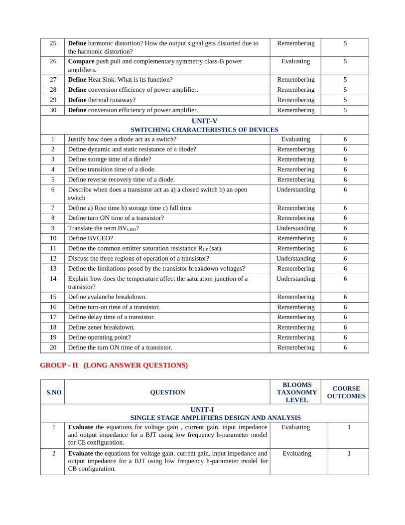
25 Define harmonic distortion? How the output signal gets distorted due to
the harmonic distortion?
Remembering 5
26 Compare push pull and complementary symmetry class-B power
amplifiers.
Evaluating 5
27 Define Heat Sink. What is its function? Remembering 5
28 Define conversion efficiency of power amplifier. Remembering 5
29 Define thermal runaway? Remembering 5
30 Define conversion efficiency of power amplifier. Remembering 5
UNIT-V
SWITCHING CHARACTERISTICS OF DEVICES
1 Justify how does a diode act as a switch? Evaluating 6
2 Define dynamic and static resistance of a diode? Remembering 6
3 Define storage time of a diode? Remembering 6
4 Define transition time of a diode. Remembering 6
5 Define reverse recovery time of a diode. Remembering 6
6 Describe when does a transistor act as a) a closed switch b) an open
switch
Understanding 6
7 Define a) Rise time b) storage time c) fall time Remembering 6
8 Define turn ON time of a transistor? Remembering 6
9 Translate the term BVCBO? Understanding 6
10 Define BVCEO? Remembering 6
11 Define the common emitter saturation resistance RCE (sat). Remembering 6
12 Discuss the three regions of operation of a transistor? Understanding 6
13 Define the limitations posed by the transistor breakdown voltages? Remembering 6
14 Explain how does the temperature affect the saturation junction of a
transistor?
Understanding 6
15 Define avalanche breakdown. Remembering 6
16 Define turn-on time of a transistor. Remembering 6
17 Define delay time of a transistor. Remembering 6
18 Define zener breakdown. Remembering 6
19 Define operating point? Remembering 6
20 Define the turn ON time of a transistor. Remembering 6
GROUP - II (LONG ANSWER QUESTIONS)
S.NO
QUESTION
BLOOMS
TAXONOMY
LEVEL
COURSE
OUTCOMES
UNIT-I SINGLE STAGE AMPLIFIERS DESIGN AND ANALYSIS
1 Evaluate the equations for voltage gain , current gain, input impedance
and output impedance for a BJT using low frequency h-parameter model
for CE configuration.
Evaluating 1
2 Evaluate the equations for voltage gain, current gain, input impedance and
output impedance for a BJT using low frequency h-parameter model for
CB configuration.
Evaluating 1
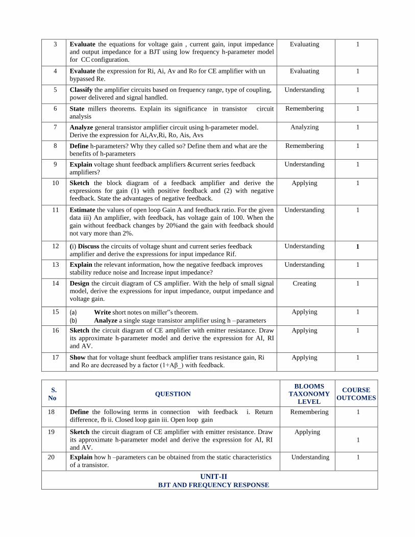
3 Evaluate the equations for voltage gain , current gain, input impedance and output impedance for a BJT using low frequency h-parameter model
for CC configuration.
Evaluating 1
4 Evaluate the expression for Ri, Ai, Av and Ro for CE amplifier with un
bypassed Re.
Evaluating 1
5 Classify the amplifier circuits based on frequency range, type of coupling,
power delivered and signal handled.
Understanding 1
6 State millers theorems. Explain its significance in transistor circuit analysis
Remembering 1
7 Analyze general transistor amplifier circuit using h-parameter model.
Derive the expression for Ai,Av,Ri, Ro, Ais, Avs
Analyzing 1
8 Define h-parameters? Why they called so? Define them and what are the benefits of h-parameters
Remembering 1
9 Explain voltage shunt feedback amplifiers ¤t series feedback
amplifiers?
Understanding 1
10 Sketch the block diagram of a feedback amplifier and derive the
expressions for gain (1) with positive feedback and (2) with negative feedback. State the advantages of negative feedback.
Applying 1
11 Estimate the values of open loop Gain A and feedback ratio. For the given
data iii) An amplifier, with feedback, has voltage gain of 100. When the
gain without feedback changes by 20%and the gain with feedback should
not vary more than 2%.
Understanding 1
12 (i) Discuss the circuits of voltage shunt and current series feedback
amplifier and derive the expressions for input impedance Rif.
Understanding 1
13 Explain the relevant information, how the negative feedback improves
stability reduce noise and Increase input impedance?
Understanding 1
14 Design the circuit diagram of CS amplifier. With the help of small signal model, derive the expressions for input impedance, output impedance and
voltage gain.
Creating 1
15 (a) Write short notes on miller‟s theorem.
(b) Analyze a single stage transistor amplifier using h – parameters
Applying 1
16 Sketch the circuit diagram of CE amplifier with emitter resistance. Draw
its approximate h-parameter model and derive the expression for AI, RI
and AV.
Applying 1
17 Show that for voltage shunt feedback amplifier trans resistance gain, Ri
and Ro are decreased by a factor (1+Aβ_) with feedback.
Applying 1
S.
No
QUESTION
BLOOMS
TAXONOMY
LEVEL
COURSE
OUTCOMES
18 Define the following terms in connection with feedback i. Return
difference, fb ii. Closed loop gain iii. Open loop gain
Remembering 1
19 Sketch the circuit diagram of CE amplifier with emitter resistance. Draw
its approximate h-parameter model and derive the expression for AI, RI
and AV.
Applying 1
20 Explain how h –parameters can be obtained from the static characteristics
of a transistor.
Understanding 1
UNIT-II BJT AND FREQUENCY RESPONSE
1 Evaluate the expressions for fβ and fT. Evaluating 3
2 Discuss the effect of coupling capacitor (Cc) on low frequency response of
CE amplifier.
Understanding 3
3 Sketch the low frequency small signal model of a transistor in CB and CE
configurations and explain significance of each model.
Applying 3
4 Sketch the small-signal high-frequency circuit of a CS amplifier and derive the expression for the voltage gain.
Applying 3
5 Show that (i) hfe=gm rb‟e for a Hybrid _ model of CE amplifier. Applying 3
6 Explain how does a Ce and Cc vary with | Ic | and | VCE |. Understanding 3
7 Explain how does gm vary with | Ic | and | VCE |, T. Understanding 3
8 Evaluate the expression for current gain with resistive load. Evaluating 3
9 Justify why the gain of the amplifier decreases in the low frequency and high frequency range?
Evaluating 3
10 Evaluate the expression for the CE short-circuits current gain Ai as a function of frequency.
Evaluating 3
UNIT-III MULTIVIBRATORS, CLIPPERS AND CLAMPERS
1 Explain the working of a fiaxed-biased binary with neat diagram. Understanding 6
2 Explain the working of a non-saturated binary. What are its drawbacks? Understanding 6
3 Discuss the different methods of triggering a binary with neat sketches. Understanding 6
4 Explain the working of a Schmitt trigger with neat sketches. Understanding 6
5 Evaluate the expressions for UTP and LTP of a Schmitt trigger. Evaluating 6
6 Explain how hysteresis can be eliminated in a Schmitt trigger. Understanding 6
7 Explain the working of a collector-coupled monostable multivibrator, With
the help of a neat circuit diagram and waveforms,.
Understanding 6
8 Evaluate an expression for the gate width of a monostable multivibrator. Evaluating 6
9 Explain the working of an astable mulpivibrator. With help of a neat circuit diagram and waveforms.
Understanding 6
10 Evaluate an expression for the frequency of oscillation of astable
multivibrator.
Evaluating 6
11 Show that an astable multivibrator can be used as a voltage to frequency
convertor.
Applying 6
12 Construct the circuit of the astable multivibrator and explain how it works.
Creating 6
S.
No
QUESTION
BLOOMS
TAXONOMY
LEVEL
COURSE
OUTCOMES
13 Explain the working of a transistor clipper. With the help of a neat circuit
diagram and waveforms.
Understanding 6
14 Explain the working of a two level diode clipping. With the help of a neat
circuit diagram.
Understanding 6
15 Explain how a sine wave may be converted into square wave using a
clipping circuit.
Understanding 6
16 Explain the working of a simple diode comparator. Draw the output wave
form for a ramp input.
Understanding 6
17 Explain the working of a positive clamping circuit. With necessary
waveforms.
Understanding 6
18 Explain the working of a Negative clamping circuit. With necessary
waveforms.
Understanding 6
19 State and prove the clamping circuit theorem? Remembering 6
20 Explain the principle of clamping. What is the need for a shunting resistor R
in parallel with the diode in the basic clamping circuit?
Understanding 6
UNIT-IV
LARGE SIGNAL AMPLIFIERS, LINEAR WAVE SHAPING
1 Evaluate the expression for maximum conversion efficiency for a simple
series fed Class A power amplifier. What are the drawbacks of transformer
coupled power amplifiers?
Evaluating 5
2 Explain the method of determination of total harmonic distortion in push
pull power amplifiers using five point method.
Understanding 5
3 Define thermal resistance? Explain the thermal electrical analogy related
to a transistor with heat sink.
Remembering 5
4 Explain and analyze a transformer coupled class A power amplifier and
also define the total harmonic distortion with three point method.
Understanding 5
5 Design the circuit of a series fed class A power amplifier and analyzes it
for its efficiency and power dissipation and proves that maximum
efficiency is 25%.
Creating 5
6 Sketch the schematic of class B push-pull amplifier with complementary
symmetry configuration and explain the working of it.
Applying 5
7 Show that maximum efficiency of Class B amplifier is 78.5%. Applying 5
8 Show that maximum efficiency of Transformer coupled Class A amplifier
is 50%.
Applying 5
9 With a neat diagram explain the principle of operation of class B pushpull
amplifier.
Understanding 5
10 Sketch the schematic of class B push-pull amplifier with complementary
symmetry configuration and explain the working of it.
Applying 5
11 Explain the operation of low pass RC circuit, and also derive an
expression for the output to an exponential input?
Understanding 5
12 Evaluate an expression for the percentage Tilt of the output of a
highpass circuit with large time constant excited by a symmetrical
square wave with Zero average value.
Evaluating 6
13 Evaluate an expression for the rise time of the output of a low pass circuit
excited by a step input.
Evaluating 6
14 Discuss about a low pass RC circuit? Derive an expression of output
voltage for square wave input and draw input-output characteristics of
this circuit.
Understanding 6
S.No
QUESTION
BLOOMS
TAXONOMY
LEVEL
COURSEOU
TCOMES
15 Sketch the high- pass R-C circuit. Derive for step- voltage response of this
circuit and show the input- output characteristics of this circuit.
Applying 6
16 Sketch the response of an RC high-pass for square wave input Applying 6
17 Explain the response of an RC high-pass filter to behave as a good
differentiator.
Understanding 6
18 Evaluate the expression for power output and conversion efficiency of a
class A series fed amplifier.
Evaluating 6
UNIT-V
SWITCHING CHARACTERISTICS OF DEVICES
1 Explain the phenomenon of “latching” in a transistor switch. Understanding 6
2 Explain the behavior of a BJT as a switch in electronic circuits. Give an
example.
Understanding 6
3 Write a short note on the switching times of transistor. Applying 6
4 Explain the behavior of a BJT as a switch. Give Applications. Understanding 6
5 Explain the terms pertaining to transistor switching characteristics.
i. Rise time. ii. Delay time.iii. Turn-on time. iv. Storage time v. Fall time.
vi. Turn-off time.
Understanding 6
6 Write Short notes on:
(a) Diode switching times
(b) Switching characteristics of
transistors (c) FET as a switch.
Applying 6
7 Explain piecewise linear diode characteristics. Understanding 6
8 Explain how transistor can be used as a switch in the circuit, under what
condition a transistor is said to be „OFF‟ and „ON‟ respectively.
Understanding 7
9 Discuss how does the temperature affect the saturation junction voltages of
a transistor?
Understanding 6
10 Explain how does avalanche multiplication take place in a semiconductor
diode?
Understanding 7
GROUP - III (PROBLEMS)
S.No
QUESTION
BLOOMS
TAXONOMY
LEVEL
COURSE
OUTCOMES
UNIT-I SINGLE STAGE AMPLIFIERS DESIGN AND ANALYSIS
1 Compute current gain, voltage gain, input and output impedance of the
CB amplifier if it is driven by a voltage source of internal resistance
Rs=1k.The load impedance is RL=1K. The transistor parameters are hib=
22, hfb= -0.98, hrb=2.9×10⁻⁴, hob= 0.5μA/V.
Applying 1
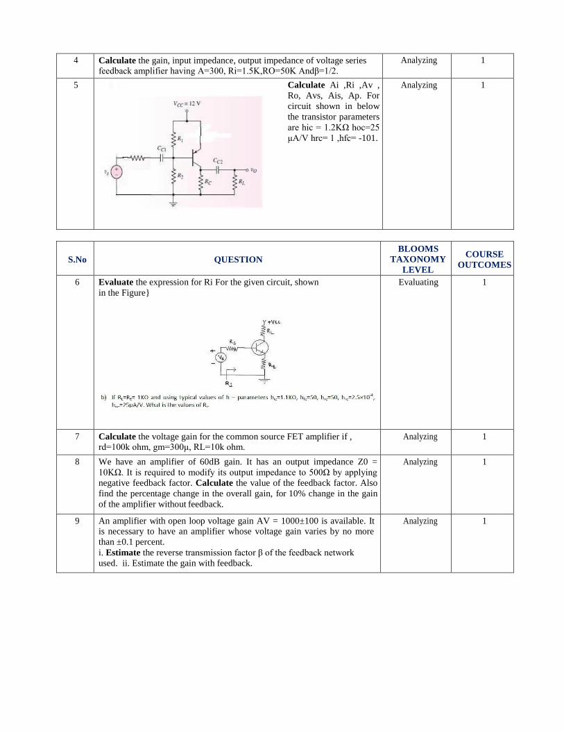
2 Calculate AI , AV , RI , R0.of a transistor with hie=1.1K, hfe=50,
hre=205X10−4 , hoe=25μA/V is connected in CE configuration as shown
in fig.
Analyzing 1
3 An Amplifier has a voltage gain of 400, f1=50Hz, f2=200KHz and a
distortion of 10% without feedback. Estimate the voltage gain, f1f , f2f
and Df when a negative feedback is applied with feedback ratio of 0.001.
Understanding
4 Calculate the gain, input impedance, output impedance of voltage series feedback amplifier having A=300, Ri=1.5K,RO=50K Andβ=1/2.
Analyzing 1
5 Calculate Ai ,Ri ,Av ,
Ro, Avs, Ais, Ap. For
circuit shown in below
the transistor parameters
are hic = 1.2KΩ hoc=25
μA/V hrc= 1 ,hfc= -101.
Analyzing 1
S.No
QUESTION
BLOOMS
TAXONOMY
LEVEL
COURSE
OUTCOMES
6 Evaluate the expression for Ri For the given circuit, shown
in the Figure
Evaluating 1
7 Calculate the voltage gain for the common source FET amplifier if , rd=100k ohm, gm=300μ, RL=10k ohm.
Analyzing 1
8 We have an amplifier of 60dB gain. It has an output impedance Z0 =
10KΩ. It is required to modify its output impedance to 500Ω by applying
negative feedback factor. Calculate the value of the feedback factor. Also
find the percentage change in the overall gain, for 10% change in the gain
of the amplifier without feedback.
Analyzing 1
9 An amplifier with open loop voltage gain AV = 1000±100 is available. It is necessary to have an amplifier whose voltage gain varies by no more
than ±0.1 percent.
i. Estimate the reverse transmission factor β of the feedback network
used. ii. Estimate the gain with feedback.
Analyzing 1
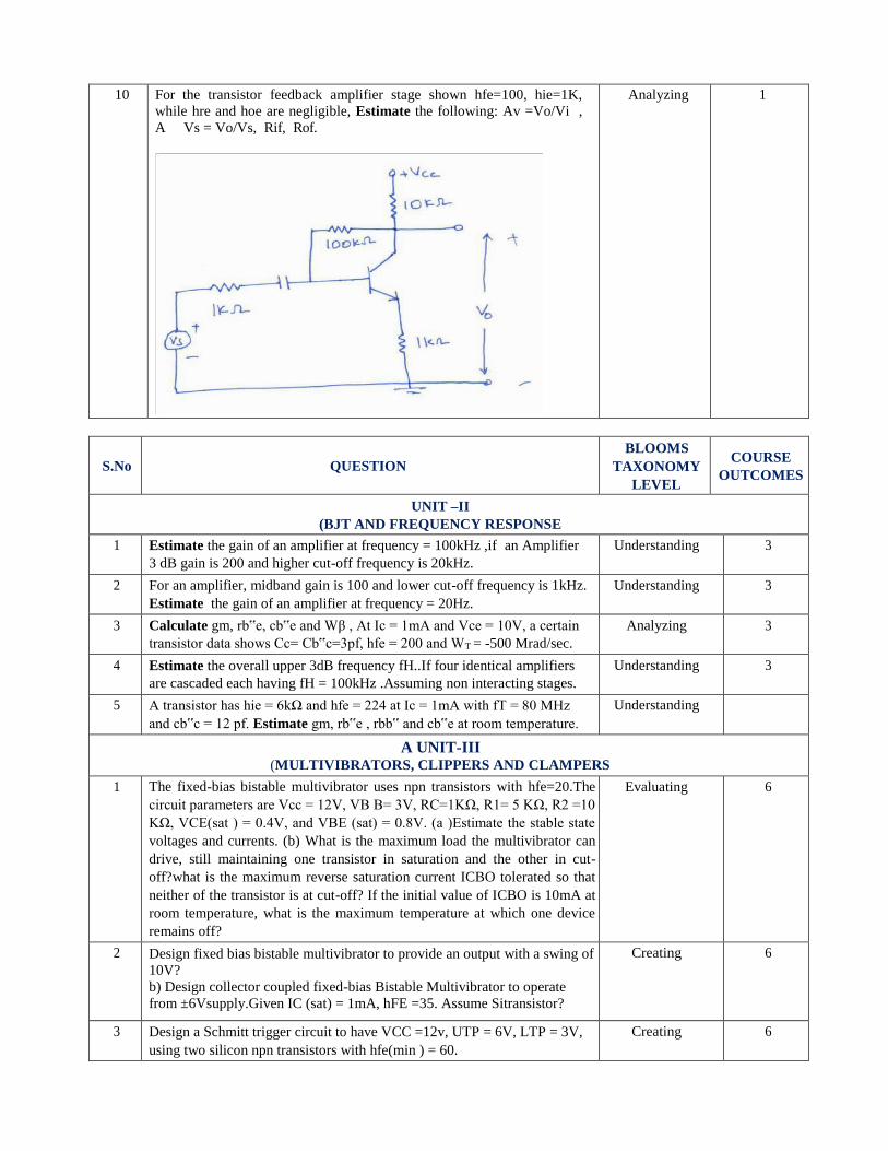
10 For the transistor feedback amplifier stage shown hfe=100, hie=1K, while hre and hoe are negligible, Estimate the following: Av =Vo/Vi ,
A Vs = Vo/Vs, Rif, Rof.
Analyzing 1
S.No
QUESTION
BLOOMS
TAXONOMY
LEVEL
COURSE
OUTCOMES
UNIT –II
(BJT AND FREQUENCY RESPONSE
1 Estimate the gain of an amplifier at frequency = 100kHz ,if an Amplifier
3 dB gain is 200 and higher cut-off frequency is 20kHz.
Understanding 3
2 For an amplifier, midband gain is 100 and lower cut-off frequency is 1kHz.
Estimate the gain of an amplifier at frequency = 20Hz.
Understanding 3
3 Calculate gm, rb‟e, cb‟e and Wβ , At Ic = 1mA and Vce = 10V, a certain
transistor data shows Cc= Cb‟c=3pf, hfe = 200 and WT = -500 Mrad/sec.
Analyzing 3
4 Estimate the overall upper 3dB frequency fH..If four identical amplifiers
are cascaded each having fH = 100kHz .Assuming non interacting stages.
Understanding 3
5 A transistor has hie = 6kΩ and hfe = 224 at Ic = 1mA with fT = 80 MHz
and cb‟c = 12 pf. Estimate gm, rb‟e , rbb‟ and cb‟e at room temperature.
Understanding
A UNIT-III (MULTIVIBRATORS, CLIPPERS AND CLAMPERS
1 The fixed-bias bistable multivibrator uses npn transistors with hfe=20.The
circuit parameters are Vcc = 12V, VB B= 3V, RC=1KΩ, R1= 5 KΩ, R2 =10
KΩ, VCE(sat ) = 0.4V, and VBE (sat) = 0.8V. (a )Estimate the stable state
voltages and currents. (b) What is the maximum load the multivibrator can
drive, still maintaining one transistor in saturation and the other in cut-
off?what is the maximum reverse saturation current ICBO tolerated so that
neither of the transistor is at cut-off? If the initial value of ICBO is 10mA at
room temperature, what is the maximum temperature at which one device
remains off?
Evaluating 6
2 Design fixed bias bistable multivibrator to provide an output with a swing of
10V?
b) Design collector coupled fixed-bias Bistable Multivibrator to operate
from ±6Vsupply.Given IC (sat) = 1mA, hFE =35. Assume Sitransistor?
Creating 6
3 Design a Schmitt trigger circuit to have VCC =12v, UTP = 6V, LTP = 3V,
using two silicon npn transistors with hfe(min ) = 60.
Creating 6
4 Estimate the period of output and the frequency of oscillation of an astable
multivibrator with R1 = R2 = 25 KΩ and C1 = C2 = 0.2μF.
Evaluating 6
5 Calculate the input pulse width of mono-stable multivibrator for the
design values of RC=2k Ω, RB=10k Ω;C =0.1 μ F , VCC =10 V ,
VBE(sat)=0.8V.
Analyzing 6
6 In an astable multivibrator circuit shown in the figure 7.4 R1=R2=5kΩ,
R3=R4=0.4kΩ and C1=C2=0.02μF. Estimate the time period and
frequency of oscillators.
Evaluating 6
7 Design a Schmitt trigger circuit using NPN transistors having hFE(min)
=60 . VBE(Cutoff) = 0V, VCE(Sat) = 0.2V and VBE(sat) = 0.7V. Given
VCC =8V and o/p swing = 6V, UTP = 3.5V, LTP = 1.5V, R1 = 10K and R2
= 2K.
Determine RC1, RC2 and Re.
Creating 6
8 Design an astable multivibrator to generate a 5kHz square wave with a dutycycle of 60% and amplitude 12v. Use NPN silicon transistors having
hFE(min) = 70 VCE(Sat) b= 0.3v, VBE(Sat) = 0.7v, VBE(Cutoff) = 0v and RC = 2K. Draw the waveforms seen at both collectors and bases.
Creating 6
S.No
QUESTION
BLOOMS
TAXONOMY
LEVEL
COURSE
OUTCOMES
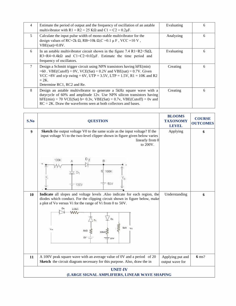
9 Sketch the output voltage V0 to the same scale as the input voltage? If the
input voltage Vi to the two-level clipper shown in figure given below varies
linearly from 0
to 200V.
Applying 6
10 Indicate all slopes and voltage levels .Also indicate for each region, the
diodes which conduct. For the clipping circuit shown in figure below, make
a plot of Vo versus Vi for the range of Vi from 0 to 50V.
Understanding 6
11 A 100V peak square wave with an average value of 0V and a period of 20
Sketch the circuit diagram necessary for this purpose. Also, draw the in
Applying put and
output wave for
6 ms?
UNIT-IV
(LARGE SIGNAL AMPLIFIERS, LINEAR WAVE SHAPING
1 Calculate the following for the given data. i. Power dissipation of each
transistor ii. Efficiency A complementary push pull amplifier has
capacitive coupled load RL=8Ω, supply voltage of.12V
Analyzing 6
2 Estimate the value of thermal resistance? If the junction temperature of a
transistor is 1250C. The total dissipation at a 250C case temperature is 0.5W
and at a 250C ambient temperature, the total dissipation is 0.2W
Evaluating 5
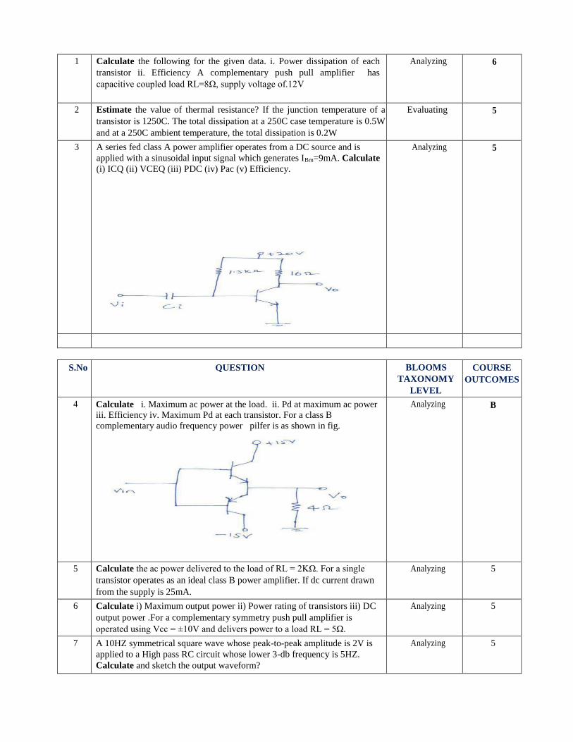
3 A series fed class A power amplifier operates from a DC source and is
applied with a sinusoidal input signal which generates IBm=9mA. Calculate (i) ICQ (ii) VCEQ (iii) PDC (iv) Pac (v) Efficiency.
Analyzing 5
S.No QUESTION BLOOMS
TAXONOMY
LEVEL
COURSE
OUTCOMES
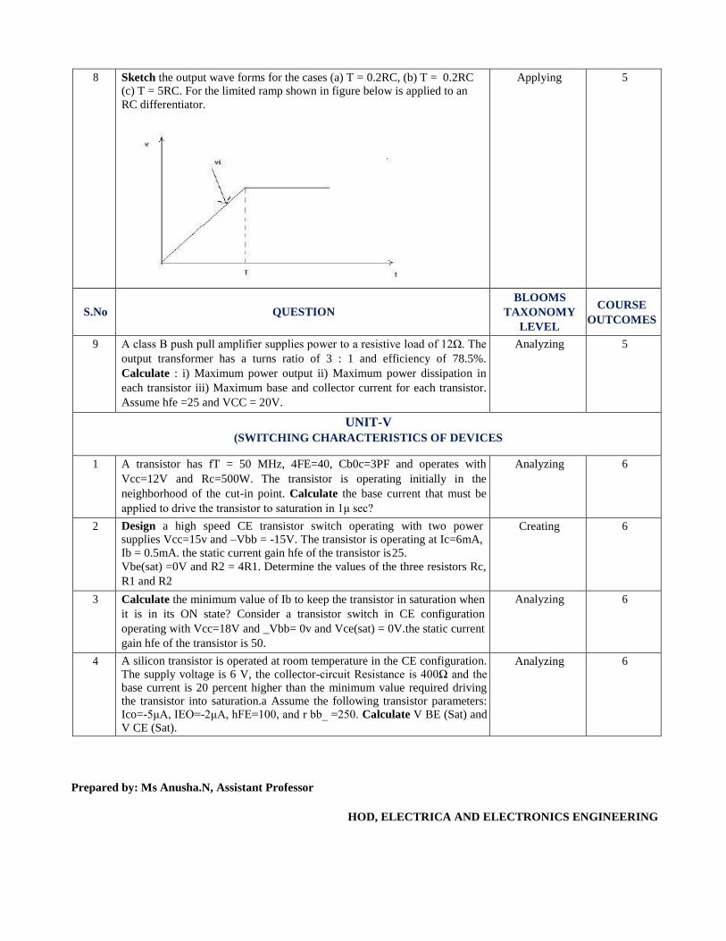
4 Calculate i. Maximum ac power at the load. ii. Pd at maximum ac power iii. Efficiency iv. Maximum Pd at each transistor. For a class B
complementary audio frequency power pilfer is as shown in fig.
Analyzing B
5 Calculate the ac power delivered to the load of RL = 2KΩ. For a single
transistor operates as an ideal class B power amplifier. If dc current drawn
from the supply is 25mA.
Analyzing 5
6 Calculate i) Maximum output power ii) Power rating of transistors iii) DC
output power .For a complementary symmetry push pull amplifier is
operated using Vcc = ±10V and delivers power to a load RL = 5Ω.
Analyzing 5
7 A 10HZ symmetrical square wave whose peak-to-peak amplitude is 2V is
applied to a High pass RC circuit whose lower 3-db frequency is 5HZ.
Calculate and sketch the output waveform?
Analyzing 5
8 Sketch the output wave forms for the cases (a) T = 0.2RC, (b) T = 0.2RC (c) T = 5RC. For the limited ramp shown in figure below is applied to an
RC differentiator.
Applying 5
S.No
QUESTION
BLOOMS
TAXONOMY
LEVEL
COURSE
OUTCOMES
9 A class B push pull amplifier supplies power to a resistive load of 12Ω. The
output transformer has a turns ratio of 3 : 1 and efficiency of 78.5%.
Calculate : i) Maximum power output ii) Maximum power dissipation in
each transistor iii) Maximum base and collector current for each transistor.
Assume hfe =25 and VCC = 20V.
Analyzing 5
UNIT-V
(SWITCHING CHARACTERISTICS OF DEVICES
1 A transistor has fT = 50 MHz, 4FE=40, Cb0c=3PF and operates with
Vcc=12V and Rc=500W. The transistor is operating initially in the
neighborhood of the cut-in point. Calculate the base current that must be
applied to drive the transistor to saturation in 1μ sec?
Analyzing 6
2 Design a high speed CE transistor switch operating with two power supplies Vcc=15v and –Vbb = -15V. The transistor is operating at Ic=6mA,
Ib = 0.5mA. the static current gain hfe of the transistor is 25.
Vbe(sat) =0V and R2 = 4R1. Determine the values of the three resistors Rc,
R1 and R2
Creating 6
3 Calculate the minimum value of Ib to keep the transistor in saturation when
it is in its ON state? Consider a transistor switch in CE configuration
operating with Vcc=18V and _Vbb= 0v and Vce(sat) = 0V.the static current
gain hfe of the transistor is 50.
Analyzing 6
4 A silicon transistor is operated at room temperature in the CE configuration. The supply voltage is 6 V, the collector-circuit Resistance is 400Ω and the base current is 20 percent higher than the minimum value required driving the transistor into saturation.a Assume the following transistor parameters: Ico=-5μA, IEO=-2μA, hFE=100, and r bb_ =250. Calculate V BE (Sat) and V CE (Sat).
Analyzing 6
Prepared by: Ms Anusha.N, Assistant Professor
HOD, ELECTRICA AND ELECTRONICS ENGINEERING