Embed Size (px)
Citation preview

PHYSICAL REVIEW B VOLUME 47, NUMBER 23 1S JUNE 1993-I
Intersubband transitions in a p-type 5-doped SiGe/Si quantum well
S. K. Chun, D. S. Pan, and K. L. WangDepartment ofElectrical Engineering, Deuice Research Laboratory, 66 14-7 Engineering IV,
Uniuersity of California, Los Angeles, California 90024(Received 14 December 1992)
The absorption spectrum in a p-type Si/Sio 6Geo 4/Si structure with a 5-doped quantum well grown on
the Si(001) substrate is calculated. For the bound-to-bound intersubband transitions, the depolarizationeffect due to the complicated couplings among valence bands is included and the inclusion of this effect
is found to be essential in understanding the absorption spectrum. The effects of subband multiplicity,
nonparabolicity, and valence-band anisotropy are also incorporated into an implicit formula for an
effective plasma frequency in order to facilitate the calculation. For the bound-to-continuum intersub-
band transition, the large-box model is adopted to circumvent the difficulty in normalizing the traveling
wave function of the continuum state. The depolarization effect is not significant for the latter bound-
to-contiuum transition because of the small overlap of the initial- and final-state wave functions. In this
case, the absorption for the normal-incidence light becomes larger than that for the parallel-incidence
light. The total absorption including the bound-to-bound and bound-to-continuum intersubband transi-
tions shows a good agreement with the experimental data. The results provide a better understanding ofintersubband transition in the valence band and further show that normal-incidence transitions can besignificant.
I. INTRODUCTION
Intersubband transitions in quantum wells have at-tracted a great deal of interest due to the potential appli-cations in modulators and infrared (IR) detectors. ' Theintersubband transition energy in the quantum well iseasily tunable by varying the quantum-well width andbarrier height. Moreover, there is a potential for the fa-brication of uniform IR detector arrays with large area.West and Eglash' reported the intersubband transitionsusing an n-type GaAs/Al Ga, As quantum-well struc-ture, and thereafter much progress has been made inmaking IR detectors and arrays. For the n-typeGaAs/Al Ga, As quantum-well structure, only the op-tical field parallel to the quantum-well growth direction(designated the z polarization) causes the intersubbandtransition. ' This is due to the fact that electron motionin the quantum-well direction (the z direction) is neces-sary for the intersubband transition of a spherically sym-metric valley. Such motion can only be induced by theoptical field along the quantum-well direction. For an n-
type SiGe/SiGe quantum-well structure, however, thepolarization selection rule stated above can be changeddue to the anisotropic mass tensor of the ellipsoidal val-leys. The optical field polarized normal to the quantum-well growth direction (the x polarization) can induce in-tersubband transitions depending on the growth direc-tion. ' Also, the oscillator strength for the intersubbandhas been shown to depend on the growth direction andthe strain condition.
Recently, p-type quantum wells have also been demon-strated to have possible applications for IR detectors. Adetailed calculation of the transitions among the valencebands for p-type GaAs/Al„Ga, As quantum wells indi-cates that both x- and z-polarized fields can induce the
absorption due to the couplings between the s-type con-duction band and p-type valence bands (s-p coupling).This result suggests a normal incidence application forthe IR detector, the modulator, and other optical devices.
More recently, the intersubband transitions in p-typeSiGe/Si heterostructures with a 6-doped quantum we11
have been experimentally demonstrated by Park,Karunasiri, and Wang. ' In that paper, the observedtransition peak in the 6-pm range was explained to be theconfined-to-confined transition between two heavy-holesubbands. Another peak in the 3-pm range was attribut-ed to the bound-to-continuum transition. The experi-mental data for the bound-to-bound transition cannot beunderstood from the model of Chang and James, whoused a two-band model to treat the p-typeAl Ga, „As/GaAs quantum well for the bound-to-bound transition. First of all, with the framework ofChang and James, one cannot explain the unusuallylarge width of the peak observed by Park, Karunasiri,and Wang. Moreover, there is only one peak, and transi-tions among various different valence bands appear ab-sent.
For the bound-to-continuum intersubband transitionobserved in the work of Park, Karunasiri, and Wang, theabsorption for the x-polarized field is the strongest. TheBloch function of the ground heavy-hole band is only afunction of the plane directions, and thus the largest ab-sorption occurs for the polarized field along the plane'(normal incidence). This fact is true for the first-orderapproximation. However, since the valence bands arestrongly coupled among them as we11 as with the conduc-tion band, the depolarization dependence becomes morecomplicated. Previously, Allen, Tsui, and Vinter" andAndo' formulated the effect of depolarization in inter-subband absorption for the n-type inversion layer. In
0163-1829/93/47(23)/15638(10)/$06. 00 47 15 638 1993 The American Physical Society

47 INTERSUBBAND TRANSITIONS IN A p-TYPE 5-DOPED. . . 15 639
those cases, only the conduction band was involved andband multiplicity, nonparabolicity, and anisotropy werenot considered. Furthermore, in the case of heavy dop-ing, high Fermi level (occupying the high plane-wave vec-tor) increases the couplings, and thus complicates theselection rule. Thus a refined framework for the calcula-tion of the intersubband transition is needed.
The purpose of this work is to provide a framework tohelp understand the polarization dependence of intersub-band transitions in the heavily doped Si, Ge„/Siquantum-well structure. In this framework, we have gen-eralized the treatise of the depolarization effect used inthe n-type Si inversion layer" (for multiple subbands ofthe conduction band) and expanded to include the p-typecase including nonparabolicity, anisotropy, andmultiple-band coupling. The bound-to-continuum inter-subband transition is then calculated using a large-boxmodel and, in this case, the depolarization effect is not in-cluded due to the small overlap of the wave functions forthe bound and the continuum states. Because of the cou-pling, the subbands are no longer the pure heavy-hole(HH), light-hole (LH), or spin-orbit (SO) states away fromthe zone center. Thus the transitions among subbandsoccur in a mixed way, involving both the same type anddifferent types of Bloch states, and the definition "inter-subband transition" is used here loosely to describe the
transition among subbands, pure or mixed. The calculat-ed results cover a wide range of the absorption spectruminvolving bound-to-bound and bound-to-continuum inter-subband transitions. The calculated results are comparedwith the published experimental results and show a goodagreement.
II. INTKRSUBBAND TRANSITION
A. Quantum-well structure
In the calculation, the band structure is described us-
ing a six-band k.p method formulated by six basis func-tions, represented by the
~J,mJ ) notation in the frame-
work of single-particle theory. The s-type conductionband is taken into account perturbatively (all other bandshave been included in an approximate way with the useof the empirical mass value). We choose the quantum-well direction (the z axis) as the quantization axis of theangular momentum.
The total 6X6 Hamiltonian includes both the k.pHamiltonian' ' and the strain Hamiltonian. ' Thestrain and spin-orbit coupling terms do not lift the spindegeneracy, and thus the total 6X6 Hamiltonian matrixcan be factorized into two 3 X 3 matrices using a unitarytransformation as follows
Z, (X+j2Y) /2&3
Z2
—( Y+jX)/&6—[3 Y cos(X—2g ) +jZ j /3V2
Z3
where the elements in the lower triangle are the complexconjugates of those in the upper triangle, and the ele-ments of the Hamiltonian matrix are
Z, =(A + —,'B)(k +k )+(A B)k, +e—o,Z2=(A —
—,'B)(k +ky)+(A +B)k, eo, —
Z3=A (k +k +k, ) —b, ,
Z4=3B(k +k 2k, )+6 —,eo
XeJ~=3B ( k —k ) +j2Nk k
Y=I 'k, Y'ej"=N(k jky),eo= ', D„(e„—e, ) . —
(2)
The coefficients 2, B, and N are the inverse mass bandparameters (IMBP), and 5 is the spin-orbit splitting ener-gy. D„ is the valence-band uniaxial deformation poten-tial for (001), ' and e," is the conventional strain com-ponent. The IMBP's of SiGe alloys are obtained byLawaetz's method, ' and D„of the Sioe alloy is linearlyinterpolated assuming strain independence. ' ' The pa-rameters used in our calculation are listed in Table I.
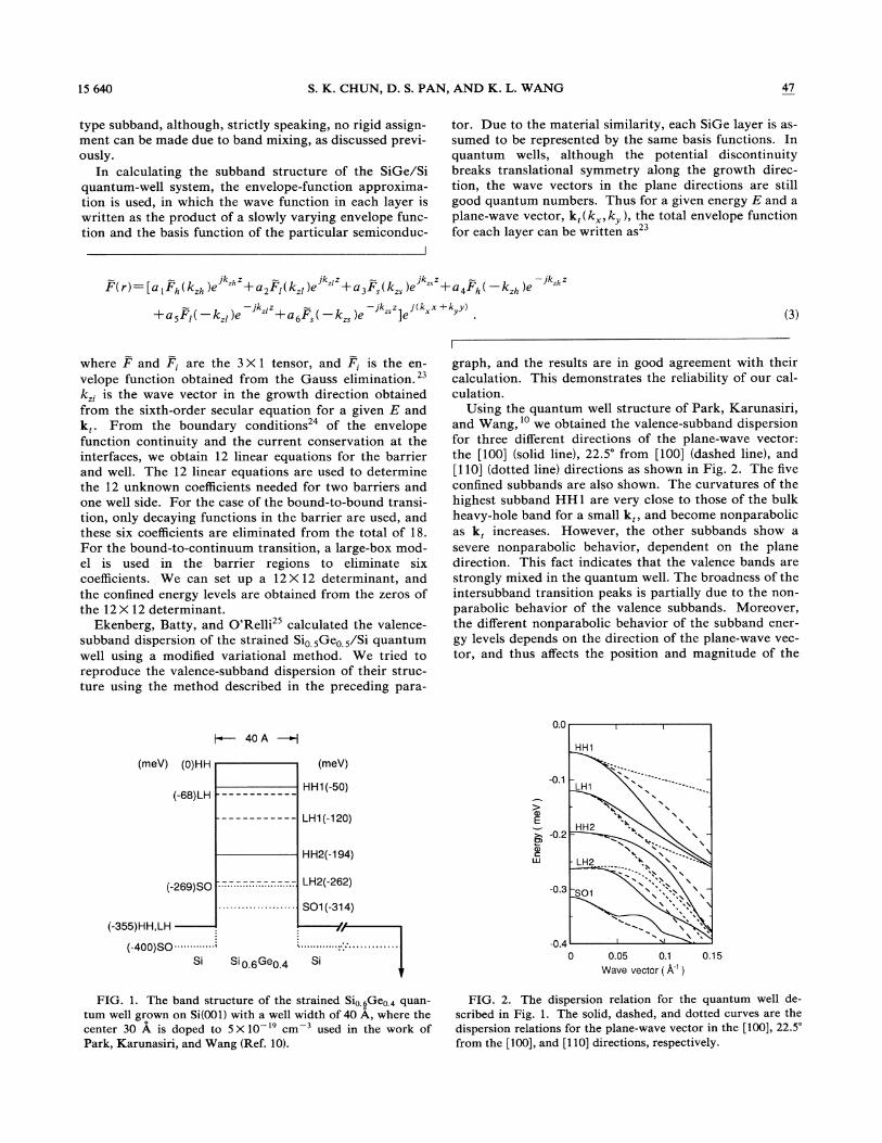
First we calculate for the quantum-well structure ofSi/Sio 6Geo ~/Si grown on Si(001) used by Park,Karunasiri, and Wang' for their experiment. The well
TABLE I. Material parameters used in this work.
Parameter
A
BXD„
—4.22 (Ref.—0.79 (Ref.—8.61 (Ref.
3.41 (Ref.
S&o.6&co.a
18) —5.43 —13.30 (Ref. 18)18) —1.47 —8.50 (Ref. 18)18) —11.47 —34.14 (Ref. 18)31) 3.37 3.32 (Ref. 32)
Unit
a.u.a.u.a.u.eV
width is taken to be 40 A, in which the center 30 A of thewell are 5 doped, with a doping level of 5X10' cmThe potential discontinuity is obtained using the band-offset calculations of Van de Walle and Martin ' and Peo-ple. ' As shown in Fig. 1, the valence-band top of thestrained well is taken as the zero energy level. In the cal-culation, we add 20-meV band bending for all valencebands due to the high doping concentration used. Theband bending in the well is assumed to be constant, whichgreatly simplifies the calculation. But this assumptioncauses some discrepancy in the subb and separation(13—17 meV) in comparison with that obtained by theself-consistent calculation, in which the isotropic, para-bolic, and decoupled valence bands were used. ' As willbe shown later, this discrepancy is also present in ourcase. The labels of the quantized subbands are adoptedfrom the characteristics of the basis states at the zonecenter. That is, the HH1 represents the first heavy-hole-
15 640 S. K. CHUN, D. S. PAN, AND K. L. WANG 47
type subband, although, strictly speaking, no rigid assign-ment can be made due to band mixing, as discussed previ-ously.
In calculating the subband structure of the SiGe/Siquantum-well system, the envelope-function approxima-tion is used, in which the wave function in each layer iswritten as the product of a slowly varying envelope func-tion and the basis function of the particular semiconduc-
I
tor. Due to the material similarity, each SiGe layer is as-sumed to be represented by the same basis functions. Inquantum wells, although the potential discontinuitybreaks translational symmetry along the growth direc-tion, the wave vectors in the plane directions are stillgood quantum numbers. Thus for a given energy E and aplane-wave vector, k, (k„,k ), the total envelope functionfor each layer can be written as
F(r) = [a)Fh(k, I, )e '" +a2FI(k, I )e ' +a3F, (k„)e " +a4Fh( —k,h )e
where F and F, are the 3X1 tensor, and F, is the en-velope function obtained from the Gauss elimination.k„- is the wave vector in the growth direction obtainedfrom the sixth-order secular equation for a given E andk, . From the boundary conditions of the envelopefunction continuity and the current conservation at theinterfaces, we obtain 12 linear equations for the barrierand well. The 12 linear equations are used to determinethe 12 unknown coefficients needed for two barriers andone well side. For the case of the bound-to-bound transi-tion, only decaying functions in the barrier are used, andthese six coefficients are eliminated from the total of 18.For the bound-to-continuum transition, a large-box mod-el is used in the barrier regions to eliminate sixcoefficients. We can set up a 12X12 determinant, andthe confined energy levels are obtained from the zeros ofthe 12 X 12 determinant.
Ekenberg, Batty, and O'Relli calculated the valence-subband dispersion of the strained Sio 5Geo 5/Si quantumwell using a modified variational method. We tried toreproduce the valence-subband dispersion of their struc-ture using the method described in the preceding para-
graph, and the results are in good agreement with theircalculation. This demonstrates the reliability of our cal-culation.
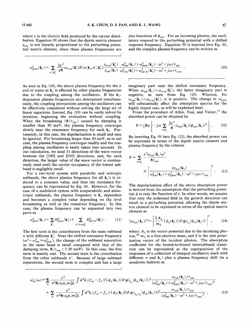
Using the quantum well structure of Park, Karunasiri,and Wang, ' we obtained the valence-subband dispersionfor three different directions of the plane-wave vector:the [100] (solid line), 22.5' from [100] (dashed line), and[110] (dotted line) directions as shown in Fig. 2. The fiveconfined subbands are also shown. The curvatures of thehighest subband HH1 are very close to those of the bulkheavy-hole band for a small k„and become nonparabolicas k, increases. However, the other subbands show asevere nonparabolic behavior, dependent on the planedirection. This fact indicates that the valence bands arestrongly mixed in the quantum well. The broadness of theintersubband transition peaks is partially due to the non-parabolic behavior of the valence subbands. Moreover,the different nonparabolic behavior of the subband ener-
gy levels depends on the direction of the plane-wave vec-tor, and thus affects the position and magnitude of the
(meV) (P)HH
40 A
(meV)
0.0
HH1
-68}LH------------(-HH1(-50)
-0.1
--- —--------I H1(-120}
H H2(-1 94)
Q)
E-0.2
CD
Q)
UJ
(-———————————— LH2(-262)-269)SO """""""""""""
SO1 (-314)
(-355)HH, LH
(-400)SO""""""*Si
~ ~'ls ~ ~ ~ ~ ~ ~ ~ ~ ~ ~ ~ ~ ~ i ~ ~ ~ ~ ~ ~ ~ ~ ~ ~ ~ ~ ~ ~
~ ~
Si0 6Ge0 4 Si
-0.40.05 0.1
Wave vector(A )
0.15
FIG. 1. The band structure of the strained Sio &Ge04 quan-tum well grown on Si(001) with a well width of 40 A, where thecenter 30 A is doped to 5X10 ' cm used in the work ofPark, Karunasiri, and Wang (Ref. 10).
FIG. 2. The dispersion relation for the quantum well de-
scribed in Fig. 1. The solid, dashed, and dotted curves are thedispersion relations for the plane-wave vector in the [100],22.5'
from the [100],and [110]directions, respectively.

47 INTERSUBBAND TRANSITIONS IN A p-TYPE 5-DOPED. . . 15 641
absorption peak for the transition away from the zonecenter.
B. Bound-to-bound intersubband transition
Generally, the intersubband transition for quantumwells with a doping concentration lower than 1X10'cm is treated elsewhere. In this case, where the many-body effect may not be important, the absorption occursat the photon energy equal to the subband separation.However, for a high carrier concentration, the absorptionpeak does not agree with the subband separation, asshown in the n-type inversion layer of Allen, Tsui, andVinter" and Ando. ' In those prior works, thediscrepancies in the absorption energy and subband sepa-ration were explained as the result of many-body effects,depolarization, excitonlike and exchange effects.For doping concentrations higher than 1 X 10' cm, thedepolarization effect is expected to be dominant in shift-ing the absorption (resonance) frequency. For a two-level system, the resonance frequency co, is shifted to ahigher frequency co„, due to plasma effects:"
CO—
CO +Q)r r p
where cop is the plasma frequency. However, the aboverule is valid only when two subbands are employed andthose subbands are assumed to be isotropic and parabol-ic. For a three-level system, Allen, Tsui, and Vinter for-mulated the absorption and showed that the coupling in-teraction gives rise to a change of the absorption lineshape when the level broadening is included. When in-
X P„*(z,k, )g (z, k, )
X(g„(k )Igloo (k )~
where v.„and co„are the lifetime and frequency for thesubband separation between the initial state m and thefinal state n, respectively, co is the incident photon fre-quency, and co/w„ indicates a level broadening. g andg„are the initial and final states, respectively, and P isthe perturbing potential as a result of photon absorption.The perturbing potential along the growth direction maybe written from Poisson's equation as
c)P e= ——An (z),2(6)
where e is the dielectric constant. From Eqs. (5) and (6),a set of coupled linear equations can be written as
volving the nonparabolic and anisotropic nature of themultiple valence subbands, as in our case, the couplinginteractions among the oscillators become essential (eachtransition being considered as an oscillator).
To include the depolarization effect in the calculationof the intersubband absorption for the valence band, wefollow the scheme of Allen, Tsui, and Vinter. However,that nonparabolicity and anisotropy were not included intheir formulation. We have included these effects in ourformulation. In doing this, the integral for the depolari-zation charge, b n (z), becomes
co„(k, )bn (z)= —2 g-
& co2 (k, ) co +—jcolr„
2e co„. (k', )—Ez„(k,)=p„(k, )+ g co„(k', ) —co +Jco/v„n', k,
(k', )S (n, k„n', k', ),
where z„(k, ) and P„(k, ) are the simplified forms of thedipole and perturbing potential matrix elements, respec-tively, for a given k, . S(n, k„n', k', ) is a product of twooverlaps of the involved wave functions as defined by Al-len, Tsui, and Vinter. " To simplify the calculation, thesquare of S(n, k„n', k', ) is evaluated as the product ofS(n, k„n, k, )XS(n', k'„n', k', ), since the evaluation ofS(n, k„n', k', ) is much more time consuming (CPU). Wehave compared these two calculations and the results arevery close. Thus for all subsequent calculations, we usethe latter to evaluate S(n, k„n', k', ). In doing this, wechoose the single particle Bloch state without includingthe effect of the random distribution of the acceptors.The effect of the random charge distribution, sometimesreferred to as a band-tailing effect, is included in the life-time w.
It should be noted that the above linear equations arek, dependent, and a large set of linear equations is neededin order to account for the subband nonparabolicity andanisotropy. Thus it becomes an immense task for compu-tation for each oscillator (between the m and n states).To circumvent this problem, instead of solving the linear
equations directly, we define a k, -dependent plasma fre-quency to account for the coupling among the oscillators:
22co~„(k, ) = g co„(kI)S (n, k„n ', kI )
eAn', k,
(k', )
co„(k', ) co +j co/~„—
co„(k, ) —co +jco/~„X
(k, )
With the complex plasma frequency defined above, therelation between the perturbing potential and optical ma-trix element shown in Eq. (7) can be rewritten as
(k, )
co„(k, ) —co +jco/~„—ez„(k, )
co„(k,)+co„„(k,) —co +jco/~„
15 642 S. K. CHUN, D. S. PAN, AND K. L. WANG 47
where c. is the electric field produced by the carrier distri-bution. Equation (9) shows that the dipole matrix elementz„ is not linearly proportional to the perturbing poten-tial matrix element, since these plasma frequencies are
also functions of P„. For an incoming photon, the oscil-lators respond to the perturbing potential with a shiftedresponse frequency. Equation (9) is inserted into Eq. (8),and the complex plasma frequency can be written as
2&', , z„(k', ) co'„(k, )+co~„(k, ) —co'+ jco/r„co „(k,)= g co„(kI)S(n,k„n', k', )
™n', k,
(10)
As seen in Eq. (10), the above plasma frequency for the n
and m states at k, is affected by other plasma frequenciesdue to the coupling among the oscillators. If the k, -
dependent plasma frequencies are determined simultane-ously, the coupling interactions among the oscillators canbe effectively considered without solving the large set oflinear equations. Instead, Eq. (10) can be easily solved byiteration, beginning the evaluation without coupling.When the broadening (Rlr„) caused by damping issmaller than 30 meV, the plasma frequency convergesslowly near the resonance frequency for each k, . For-tunately, in this case, the depolarization is small and maybe ignored. For broadening larger than 30 meV, as in ourcase, the plasma frequency converges readily and the cou-pling among oscillators is easily taken into account. Inour calculation, we used 31 directions of the wave vectorbetween the [100] and [010] directions, and, for eachdirection, the larger value of the wave vector is continu-ously used until the carrier occupancy of the lowest sub-band is negligibly small.
For a two-level system with parabolic and isotropicsubbands, the above plasma frequency for all k, 's is re-duced to a constant value, and thus the resonance fre-quency can be represented by Eq. (4). However, for thecase of a multilevel system with nonparabolic and aniso-tropic subbands, the plasma frequency is k, dependentand becomes a complex value depending on the levelbroadening as well as the transition frequency. In thiscase, the plasma frequency can be separated into twoparts as
imaginary part near the shifted resonance frequency.When co„(k,))co„. (k', ), the latter imaginary part isnegative, as seen from Eq. (10). Whereas, forco„(k,)(co„. (kI), it is positive. The change in co„„will substantially affect the absorption spectra for thehighly doped case, as will be explained later.
From the procedure of Allen, Tsui, and Vinter, " theabsorbed power can be obtained by
2 2
P =—,'Re jco g — co„(k,)lg„(k, )l
n, k,
(12)
By inserting Eq. (9) into Eq. (12), the absorbed power canbe expressed in terms of the dipole matrix element andplasma frequency by the relation
e co„(k, )coP= g A~„
Ez„(k, )
co„(k,)+co „(k,) —co +jco/r„(13)
The depolarization effect of the above absorption poweris derived from the assumption that the perturbing poten-tial P is only the function of z. In other words, we assumethat only the polarized field in the growth direction canresult in a perturbing potential, allowing the dipole ma-trix element to be expressed in terms of the optical matrixelement as
(k, )= g 0 „(k',)+ g 0 „, (k', ) .n'Wn, k,
2230(q„(k, )l(."p), lq (k, )& (14)
The first term is the contribution from the same subbandn with different k', . Near the shifted resonance frequency(co -co„+co„),the change of the subband separationin the same band is small compared with that of thedamping term, A/7„( )30 meV). In this case, the firstterm is mainly real. The second term is the contributionfrom the other subbands n'. Because of large subbandseparations, the second term is complex and has a large
where Ao is the vector potential due to the incoming pho-ton, mo is a free-electron mass, and e is the unit polar-ization vector of the incident photon. The absorptioncoeKcient for the bound-to-bound intersubband transi-tion can be represented as the superposition of theresponses of a collection of damped oscillators (each withdifferent n and k, ) plus a plasma frequency shift (in aquadratic fashion) as
e co„ (k, )/r„Jd'I, (f f„l&)@„,(kI )(p~), lg (k—, ) &I'vr %coon„moL
" " co„(k,)+cop„(k, ) —co +jco/r„
e co„(k, ) /r„+ g, , Id'I, (f —f. I)& @. (k, I )(~p .).. I g (k, ) & I'

INTERSUBBAND TRANSITIONS IN A p-TYPE 5-DOPED. . . 15 643
where L is the quantum-well width and f is the Fermidistribution function. As explained before, the first termof Eq. (11), or the plasma frequency due to the same sub-band at near the resonance frequency is mainly real. Thereal value of the plasma frequency causes the shift of theresonance peak position similar to that of Eq. (4). On theother hand, the coupling interaction from the lower sub-bands (smaller resonance energy) induces the large nega-tive imaginary part [the second term of Eq. (11)]. Thusthe coupling interaction due to the lower subbandeffectively decreases the damping constant (cols„) in
Eq. (15). In other words, it decreases the width and in-creases the absorption coefficient. Likewise, the couplinginteraction with the higher subbands effectively broadensthe absorption peak, since the higher subband (large reso-nance energy) provides a positive imaginary value.
The optical matrix element e p in Eq. (15) can be ob-tained from the k.p matrix element. The optical matrixelement has the same form as the k.p matrix element, ex-cept that k;k is replaced with k;e +k e; and multipliedby a constant factor mo/A. Then the resulting matrix istransformed by the unitary transformation which makesthe 6X 6 total Hamiltonian into two 3 X 3 Hamiltonians.The optical matrix used accounts for all directions of thepolarized electric field of the incoming light. Its elementsare as follows:
Pl 0( u, e.piu, ) =
hh Mhl Mh$
Mlh Mll Ml,
M$h M$l M$$
(16)
Ms=2(A +B)e,k, +(2A B)(E„k +e —k ), (17)
where the elements of the optical matrix are
M„h =2( 3 B)e,k, +(2—A +B)(E,k +e k~ ),1
Mh& j =—N(e, cosy —e~»ng)k, j 3N~, k, , —-3
V3B ( e k ——e k~ ) cosy1+ —N(e k +e k )siny,3
= 1Mh, = —N( —e cosr)+e sinr))k, + ,'Ne, k, —
v'6
+j v'6B (e„k, —e k ) cosy2—N(e k +e~k„)siny,6
Mlh M hl
where k, is the magnitude of the wave vector in the planedirection.
Equation (17) shows the selection rule of the intersub-band transitions for the p-type quantum well. For the in-tersubband transition involving the same type of basisfunctions (Mhh M,~, and M„), the oscillator strength isproportional to the polarized field times the wave vectorin the same direction for the isotropic band. In this case,k, is usually larger than k, for high confined energy lev-
els, resulting in a large absorption for the z-polarizedfield. On the other hand, when the multiple bands, e.g. ,the heavy- and light-hole bands (or the heavy-hole andspin-orbit bands) are involved in the subband transition,three components, e,k„e,k„and e, k, become pro-nounced. The intersubband transition due to e, k, and
e, k, becomes large only when carriers occupy the largevalue of k, (the high doping case). On the other hand,the e, k, term is larger than the other two terms due tothe large k, .
C. Bound-to-continuum intersubband transition
In the calculation of the absorption of the bound-to-continuum transition, care must be exercised in wave-function normalization. For a single-band case, the wavefunctions can be normalized by assuming that the wellwidth is negligibly narrow. However, for the multibandcase, the normalization of the wave functions is not easy,and a large-box model is used in our calculation. In thismethod, the continuum state is assumed to be confined ina large box which is ten times wider than the SiGe well,and energy levels are calculated in a manner similar tothat for the confined energy level in the quantum well.The number of subband energy levels in the large box isincreased until the absorption saturates. For the bound-to-continuum transition, the depolarization effect is notincluded in this calculation for the following reasons.For an infinitely large box or free space, the amplitude ofthe wave function in the well is extremely small. Thusthe overlap between the initial and final states is negligi-ble when compared with the bound-to-bound case. Foran extremely small wave-function overlap, the depolari-zation effect becomes negligibly small. According to theexperimental data of Park, Karunasiri, and Wang, ' thepeak position is almost independent of the polarization ofthe incident light, supporting our previous assertion.Thus the bound-to-continuum intersubband transitioncan be calculated from Eq. (15) at the zero plasma fre-quency limit as
a" (co)=a' (co)~„o, (18)M&, = j 2V2Be, + —Ne, cos(y —g) —e sin(y —rl) k,
jv'2B ( e„k +E~ k~ )—1
Ne, k, cos(y —2q),v'2
M,h =Mh, ,
M =M*sl ls
M„=2Am, k, +22 (e k +e~k ),
and the total absorption is the sum of the bound-to-bound and bound-to-continuum intersubband transitions,i.e., the sum of Eqs. (15) and (17).
III. RESULTS
Figures 3(a) and 3(b) show squared momentum matrixelements (SMM's) of the structure for the z- and x-polarized fields, respectively. We show the SMM's of theimportant intersubband transitions for the wavelength

15 644 S. K. CHUN, D. S. PAN, AND K. L. WANG
0.4I
(a) z polarization
0.3XL
65
E0.2
CD
EO
CD
0.1
C3(D
H1S1
range shorter than 10 pm. For convenience, H1L2 isdefined as the transition when the initial state is HH1 andthe final state is LH2. For the z polarization, as shown inFig. 3(a), H1H2 and L1L2 are very strong for a small k„and decrease as k, increases, whereas H1L2 is forbiddenat the zone center and becomes large for a large k, . Thisfact indicates that the heavy- and light-hole bands arestrongly coupled by means of k, ~ For low doping, wherethe carriers have a small wave vector, the absorptionstrength of the H1H2 is large. For high doping, theH1L2 peak is greatly enhanced because of the occupancyat high k, . The L1L2 transition is very similar to H1H2,and the peak position is also close to the H1H2 in thiscase. That is, only two strong peaks, H1H2 and H1L2,are expected according to the SMM since the H1H2 andL1L2 energies overlap into one peak. For the x polariza-tion, the SMM shown in Fig. 3(b) is smaller than that forthe z polarization of Fig. 3(a). Thus it is predicted for the
bound-to-bound inter subb and transition that the z-polarized transition is stronger than that for the x- or y-polarized case. It is important to note that the "bsorp-tion strength of the H1L2 does not vanish completely atthe zone center because of the optical matrix term ofe„k,. However, without the inclusion of s-p coupling, thistransition (or bulklike interband transition) is extremelyweak because of the orthogonality of the basis functions.The experimental proof will be shown later.
Figure 4 shows the absorption coescient for thebound-to-bound intersubband transitions at 300 K. Inthis figure, the depolarization effect is not included andan infinite lifetime is assumed. Two cases are used tocheck the effect of the anisotropic characteristics of thevalence subbands: one assumes the isotropic valencebands (k, ~~[100]), and the other uses the anisotropicvalence bands. The Fermi energy levels for the isotropicand anisotropic cases are 137 and 107 meV, respectively,for the doping density of 5 X 10' cm, below the top ofthe valence-band edge. The lower Fermi energy level forthe isotropic case is due to the small density of states ofthe HHl in the [100] direction. The polarization direc-tion is chosen such that the polarized field has equal xand z components (xz polarization) or the x componentonly (x polarization). The conditions are equivalent tothose used in the experiment by Park, Karunasiri, andWang' for a polarization angle of 0' or 90 with a 45'bevel angle of the waveguide. The dotted and chain-dotted curves (designated as x Iand xz I-) are for t-he x-and xz-polarized fields, respectively, for the isotropiccase, whereas the dashed and solid curves are for the an-isotropic case (designated as x-A and xz-A). The spec-trum near 9.2 pm consists of H1H2 and L1L2 as a resultof nonparabolicity. As expected from SMM's in Fig. 3,these two transitions are very strong for the xz-polarized
0.05 0.1Wave vector ( A )
0.15
0.1
O~ 0.08K
6$
0.06—E
(9Eo 0.04—
0.02
0
I
(b) x polarization
y L1L2
5EoC)
4
0)OP 3O
0
0ti)
JD1
----- x-l—- -xz-l——-x-A
xz-A
H1L2
7 8Wavelength ( pm )
HlH2 & L1L2I
io
0.05 0.1Wave vector ( A )
FICx. 3. Squared momentum matrix elements of the strainedSio 6Cxeo & quantum well grown on Si(001) between various bandswith a 40-A well width. (a) z-polarized field and (b) x-polarizedfield.
FIG. 4. The absorption coefficient of the bound-to-bound in-tersubband transitions without the depolarization efFect. Thedotted and chain-dotted curves are the absorption for the x- andxz-polarized fields, respectively, when the isotropic valencebands (x-I,xz-I) are assumed. The dashed and solid curves arefor the case when the anisotropic characteristics (x-A, xz-A)are included.

47 INTERSUBBAND TRANSITIONS IN A p-TYPE 5-DOPED. . . 15 645
field. The peak for the anisotropic case is larger thanthat for the isotropic case. This is mainly due to the k, -
dependent density of states and its SMM's. For the iso-tropic case, more carriers have larger k„where the SMMis small. For the x-polarized field, both cases give smallerpeaks than those for the xz-polarized field, similar to thepolarization dependence of the intersubband transition inthe n-type quantum well. The peak near 7 pm is due tothe transition from the ground heavy- to the excitedlight-hole subbands (H1L2), and is forbidden at the zonecenter. However, the band mixing among bands awayfrom the zone center makes the transition possible„as ex-pected from Fig. 3. The peak positions near 7 pm for thetwo cases are 10 meV apart, in contrast to the peak at 9.2pm, where there is no difference in the peak positions.This fact indicates that the absorption occurs mainlyaway from the zone center. The transition from HH1 toSO1 gives a peak near 6.2 pm. In this case, the same par-ity of envelope functions and different types of Blochstates make the peak much smaller than the others.
In Fig. 4, when the peaks from the two different polar-izations are compared, the anisotropic case shows thatthe absorption due to the xz-polarized field is muchstronger than that for the x-polarized field. However, theisotropic case does not give the strong polarizationdependence. That is, the isotropic case tends to overesti-mate the absorption for the x-polarized field. For the xz-polarized field, the H1H2 is underestimated and theH1L2 is overestimated.
As described above, the calculated absorption givestwo peaks for both the isotropic and anisotropic cases.On the other hand, the experimental result of Park,Karunasiri, and Wang' shows only one broad peak inthe region of 4-8 pm for the xz-polarized field. Severalfactors, which are not considered in our calculation, mayaccount for the difference. The scattering processes, suchas phonon, alloy, and impurity scatterings, may broadenthe peaks to some extent. Also, the band-tailing effectdue to the high doping may be important. But the in-clusion of these effects alone does not make the two peaksmerge into a single broad one. However, as shown next,the unusual broad peak in the experimental data can beexplained by the inclusion of the depolarization effect.
Including the depolarization effect, the absorptionspectra for the xz-polarized field is calculated for thebound-to-bound transition. Figure 5 shows the resultsfor this transition along with the experimental data (givenby ARE). The three calculated spectra are due todifferent considerations of the coupling among the sub-bands. The absorption from the HH1 is included onlybecause most carriers occupy this state at 300 K. The en-ergy broadenings A/~„ for each subband are assumed tobe k, independent, and a constant value of 50 meV isused. The dashed curve is for the isolated two-level sys-tem, neglecting the coupling interactions among sub-bands, but including the coupling interactions among @,-
dependent oscillators due to the subband nonparabolicityand anisotropy. The result of assuming an isolated two-level system gives a broad peak, with the peak positionnear 8 pm. This peak position is 67 meV apart from theexperimental peak. The chain-dotted curve shows the ab-
1.0
xz polarization
0.8O
0.6Q)O
Q)0u 0.4O
0th 0.2
Isotropic
0.05 6 7 8
Wavelength ( p,m )
9 10
FIG. 5. The absorption coe%cient of the bound-to-bound in-
tersubband transitions, including the depolarization effect forthe xz-polarized field at 300 K. The dashed curve is the absorp-tion calculated by using an isolated two-level system andvalence-band anisotropy. The chain-dotted curve is for a cou-pled multilevel system when the plane-wave vector in the [100]direction is used only (assuming isotropic). The solid curve isfor the coupled multilevel system with the valence band anisot-ropy. The symbol E denotes the experimental data (Ref. 10).
sorption when the coupling of the multilevel transitionsplus band nonparabolicity is included, and the isotropicvalence band is assumed. As mentioned earlier, the cou-pling of other subbands suppresses the absorption of theH1H2 transition (the lower resonance energy), whileenhancing the H1L2 transition (the higher resonance en-ergy). In this case, the peak position occurs at 6.4 pm,and the full width at half maximum (FWHM) is about 75meV. The peak position is 30 meV apart from the experi-mental data, and the FWHM is somewhat narrower.When the valence-band anisotropy plus nonparabolicityand multiple subbands are included, the FWHM becomes95 meV and the peak position moves to near 6.3 pm, andthey are very close to the experimental data. The smalldifference of the peak position (17 meV) may be due tothe lack of a self-consistent calculation. The self-consistent calculation done by Park, Karunasiri, andWang' shows that the subband separation is 13-17meV larger than ours. From the above results, the exper-imental data of the bound-to-bound intersubband transi-tion can only be explained when the depolarization effect,subband multiplicity, and subband anisotropy are in-voked.
For the bound-to-continuum intersubband transition,Fig. 6 shows the measured and calculated spectra for thex polarization (normal incidence), where the absorptionsfrom the HH1 and LH1 are included. The experimentaldata are given with the free-carrier contribution removedand the experimental data of the intersubband transitionequal our calculation at 4.6 pm for 40% Ge and 3.6 pmfor 60% Ge, respectively. The depolarization effect is notincluded in this case for the reason explained above. Inour calculation, the direct conduction band is not explic-

15 646 S. K. CHUN, D. S. PAN, AND K. L. WANG 47
2000
E 1500
Q)0~oh 000
500
Ge 60 '/o e~ ~
x polarization
0.7
0.6E
0.5
g 0.4Q
o 0.3
p. 0.2O
~ 0&
03
Wavelength ( N.m )
0 )
2 6Wavelength ( pm )
FIG. 6. The calculated absorption coe%cient of the bound-to-continuum intersubband transitions for the x-polarized fieldat 300 K. The solid and dashed curves are the absorption forthe Ge 40% and 60%%uo quantum wells, respectively. Experimen-tal data (Ref. 10) (shown in E and ) are also given for compar-ison.
itly used as a basis function. However, the s-p couplinginteraction of the direct conduction band is treated as aperturbation term. Each calculated absorption spectrumhas two peaks, due to two initial states: the heave-hole(HH1) and light-hole (LH1) ground states. As can beclearly seen for the 607o Ge we11 case, the increase in ab-sorption strength at 2.5 pm comes from the heavy-holeground state HH1. This contribution is larger than theother because of its larger carrier occupancy.
As the Ge content of the well increases, the peak posi-tion shifts to the lower-wavelength (higher-energy) regionand its peak height increases. The lower peak positionfor the 60% Ge well is due mainly to the larger bandoffset of the quantum well. On the other hand, thechange of the peak heights ean be understood from thes-p coupling between the s characteristic of the directconduction band (I z) and the p-characteristic valenceband (I z~). This coupling strength is proportional to thesquare of the wave vector and inversely proportional tothe square of the direct energy gap to the first order. Be-cause the continuum state for the 60% G-e quantum wellhas the larger k, and smaller direct energy gap, the s-pcoupling for the 60% Ge quantum well becomes largerand thus gives the larger peak height.
In the data of Figs. 5 and 6, we have explained the ab-sorption coefficient of the bound-to-bound transition forthe xz polarization and the bound-to-continuum transi-tion for the x polarization. However, the polarizationdependence of the absorption has not been discussed.Figure 7 shows the polarization dependence of the calcu-lated absorption spectra and the experimental data of40% Ge quantum wells for the bound-to-bound andbound-to-continuum intersubband transitions. Thecurves with symbols are experiment data (A for the x po-larization and ~ for the xz polarization), whereas thedashed and solid curves are the theoretical calculationsfor the x and xz polarizations, respectively. Because of
FIG. 7. The absorption coefficient for the strained Sio 6Ge040
quantum well grown on Si(001) with a 40-A well width, ~herethe center 30 A are doped with up to 5X19 cm . Symbolswith 4 and 0 are experimentally obtained absorptioncoe%cients for the x- and yz-polarized fields, respectively. Thedashed and solid curves are the theoretical calculations for thecorresponding fields. The experimentally obtained values in-
clude the free-carrier absorption.
the free-carrier contribution whose quantity cannot beaccurately estimated, ii is dificult to compare the abso-lute peak heights, but the trend of the polarization depen-dence of the calculated absorption coefficients shows agood agreement with the experimental data. For the x-polarized field (normal incidence), the peak near 3.2 pmagrees well for the calculated and experimental spectra.In this case, the discrepancy between the experiment andcalculation increases as the wavelength increases. This isexpected to be due to the free-carrier absorption in theexperiment data. For the xz-polarized 6eld, the calcula-tion (solid curve) gives a small peak near 3.2 pm while noclear peak is seen in the experimental data. The reasonfor this discrepancy is not clear. When the peak positionof the bound-to-bound transition near 6.2 pm is shiftedtoward the experimentally obtained peak position (5.9pm), or when the large broadening is chosen, the smallpeak may be buried in the broad peak. It should be not-ed, however, that for the 60% Ge quantum-well case, thissmall peak was obtained experimentally to be in agree-ment with the calculation (although difFerent in energy).In short, our calculation shows a good agreement withthe experimental data.
IV. SUMMARY
The absorption spectra for the intersubband, bound-to-bound, and bound-to-continuum transitions in the p-type 5-doped quantum well were calculated with andwithout the depolarization effect. For the bound-to-bound intersubband transition, the energy and the widthof the experimental peak can only be explained by consid-ering the depolarization effect, including complicatedeffects due to the band-coupling interactions among thevalence bands. For the bound-to-continuum transition,the depolarization effect seems not as important. The in-
dependence of the absorption peak position from the po-

47 INTERSUBBAND TRANSITIONS IN A p-TYPE 5-DOPED. . . 15 647
larization angle in the experiment supports this fact. Ingeneral, the peak positions and absorption coefficients arein good agreement with the experimental data for variousGe contents of the well layer. Our calculation clearly ex-plains the polarization dependence of the bound-to-boundand bound-to-continuum transitions in p-type SiGe quan-tum wells.
ACKNOWLEDGMENTS
One of the authors (S.K.C.) would like to thank Dr. R.P. G. Karunasiri for helpful discussions and supportivedata. This paper was supported in part by the Air ForceOfBce of Scientific Research and the Army ResearchOffice.
L. C. West and S. J. Eglash, Appl. Phys. Lett. 46, 1156 (1985).B. F. Levine, K. K. Choi, C. G-. Bethea, J. Walker, and R. J.
Malik, Appl. Phys. Lett. 50, 1092 {1987).B.F. Levine, R. J. Malik, J. Walker, K. K. Choi, C. G. Bethea,
D. A. Kleinman, and J. M. Vandenberg, Appl. Phys. Lett. 50,273 (1987).
4B. F. Levine, C. G. Bethea, K. K. Choi, J. Walker, and R. J.Malik, J. Appl. Phys. 64, 1591 (1988).
5B. F. Levine, C. G. Bethea, G. Hasnain, J. Walker, and R. J.Malik, Appl. Phys. Lett. 53, 296 (1988).
C. L. Yang and D. S. Pan, J. Appl. Phys. 64, 1573 (1988).7C. L. Yang, D. Pan, and R. Somoano, J. Appl. Phys. 65, 3253
(1989).8S. K. Chun and K. L. Wang, Phys. Rev. B 46, 7682 (1992).Y. C. Chang and R. B. James, Phys. Rev. B 39, 12 672 (1989).J. S. Park, R. P. G. Karunasiri, and K. L. Wang, Appl. Phys.Lett. 60, 103 (1992).S. J. Allen, D. C. Tsui, and B. Vinter, Solid State Commun.20, 425 (1976).
I T. Ando, Z. Phys. B 26, 263 (1977).G. Dresselhaus, A. F. Kip, and C. Kittel, Phys. Rev. 98, 368(1955).
'4J. M. Luttinger, Phys. Rev. 102, 1030 (1956).'5H. Hasegawa, Phys. Rev. 129, 1029 {1963).
D. A. Broido and L. J. Sham, Phys. Rev. B 31, 888 (1985).R. People, Phys. Rev. B 32, 1405 (1985).
8P. Lawaetz, Phys. Rev. B 14, 3460 (1971).'9R. People, IEEE J. Quantum Electron. QE-22, 1696 (19861.
S. K. Chun and K. L. Wang, IEEE Trans. Electron. Devices39, 2153 (1992).C. G. Van de Walle and R. M. Martin, Phys. Rev. B 34, 5621(1986).R. P, G. Karunasiri (private communication).R. Wessel and M. Altarelli, Phys. Rev. B 40, 12457 (1989).M. Altarelli, Phys. Rev. B 28 842 (1983).U. Ekenberg, W. Batty, and E. P. O'Relli, J. Phys. (Paris) 48,553 (1987).B.Vinter, Phys. Rev. Lett. 35, 598 (1975).T. Ando, Phys. Rev. B 13, 3468 (1976).
2sB. K. Ridley, Quantum Processes in Semiconductors (OxfordUniversity Press, London, 1982).E. O. Kane, J. Phys. Chem. Solids 1, 82 (1956).From the experimental data, the A/~ is expected to be 50—100meV. Here even the lowest value of the energy broadening isused, and the observed peak in the experiment is well ex-plained.I. Balslev and P. Lawaetz, Phys. Lett. A 19, 6 (1965).J. C. Hensel and K. Suzuki, Phys. Rev. B 9, 4219 (1974).