Embed Size (px)
Citation preview
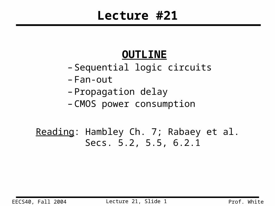
Lecture 21, Slide 1EECS40, Fall 2004 Prof. White
Lecture #21
OUTLINE– Sequential logic circuits– Fan-out– Propagation delay– CMOS power consumption
Reading: Hambley Ch. 7; Rabaey et al. Secs. 5.2, 5.5, 6.2.1

Lecture 21, Slide 2EECS40, Fall 2004 Prof. White
Flip-Flops
• One of the basic building blocks for sequential circuits is the flip-flop:– 2 stable operating states stores 1 bit of info.– A simple flip-flop can be constructed using two
inverters:
Q
Q

Lecture 21, Slide 3EECS40, Fall 2004 Prof. White
• Rule 1:– If S = 0 and R = 0, Q does not change.
• Rule 2: – If S = 0 and R = 1, then Q = 0
• Rule 3:– If S = 1 and R = 0, then Q = 1
• Rule 4:– S = 1 and R = 1 should never occur.
The S-R (“Set”-“Reset”) Flip-Flop
S
R
QS-R Flip-Flop Symbol:
Q

Lecture 21, Slide 4EECS40, Fall 2004 Prof. White
Realization of the S-R Flip-Flop
S
R
Q
Q
R S Qn
0 0 Qn-1
0 1 11 0 01 1 (not allowed)

Lecture 21, Slide 5EECS40, Fall 2004 Prof. White
Clock Signals
• Often, the operation of a sequential circuit is synchronized by a clock signal :
• The clock signal regulates when the circuits respond to new inputs, so that operations occur in proper sequence.
• Sequential circuits that are regulated by a clock signal are said to be synchronous.
time
vC(t)
VOH
0TC 2TC
positive-going edge(leading edge)
negative-going edge(trailing edge)
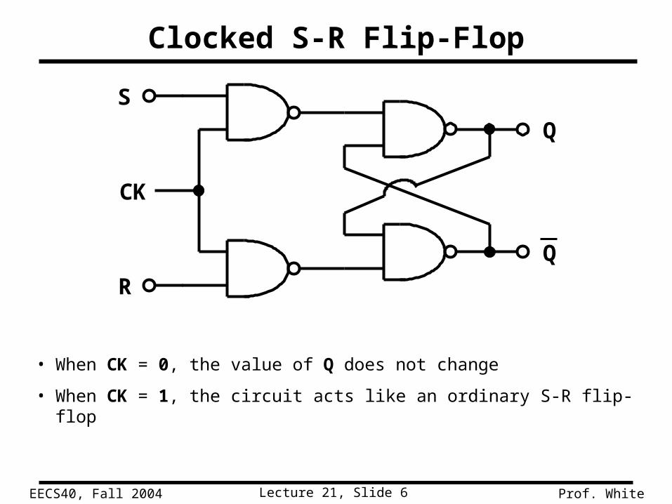
Lecture 21, Slide 6EECS40, Fall 2004 Prof. White
Clocked S-R Flip-Flop
• When CK = 0, the value of Q does not change
• When CK = 1, the circuit acts like an ordinary S-R flip-flop
S
R
Q
Q
CK

Lecture 21, Slide 7EECS40, Fall 2004 Prof. White
• The output terminals Q and Q behave just as in the S-R flip-flop.
• Q changes only when the clock signal CK makes a positive transition.
The D (“Delay”) Flip-Flop
D
CK
QD Flip-Flop Symbol:
Q
CK D Qn
0 Qn-1
1 Qn-1
0 0 1 1

Lecture 21, Slide 8EECS40, Fall 2004 Prof. White
D Flip-Flop Example (Timing Diagram)
t
CK
t
D
t
Q

Lecture 21, Slide 9EECS40, Fall 2004 Prof. White
Registers
• A register is an array of flip-flops that is used to store or manipulate the bits of a digital word.
Example: Serial-In, Parallel-Out Shift Register
D0
CK
Q0Data input
Clock input
D1
CK
Q1 D2
CK
Q2
Q0 Q1 Q2Parallel outputs

Lecture 21, Slide 10EECS40, Fall 2004 Prof. White
Conclusion (Logic Circuits)
• Complex combinational logic functions can be achieved simply by interconnecting NAND gates (or NOR gates).
• Logic gates can be interconnected to form flip-flops.
• Interconnections of flip-flops form registers.
• A complex digital system such as a computer consists of many gates, flip-flops, and registers. Thus, logic gates are the basic building blocks for complex digital systems.
Lecture 21, Slide 11EECS40, Fall 2004 Prof. White
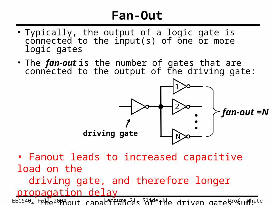
Fan-Out• Typically, the output of a logic gate is connected
to the input(s) of one or more logic gates
• The fan-out is the number of gates that are connected to the output of the driving gate:
•••
fan-out =N
driving gate
1
2
N
• Fanout leads to increased capacitive load on the driving gate, and therefore longer propagation delay
– The input capacitances of the driven gates sum, and must be charged through the equivalent resistance of the driver

Lecture 21, Slide 12EECS40, Fall 2004 Prof. White
Effect of Capacitive Loading
• When an input signal of a logic gate is changed, there is a propagation delay before the output of the logic gate changes. This is due to capacitive loading at the output.
CL
+
vOUT
+vIN
vIN
vOUT
The propagation delay ismeasured between the50% transition points ofthe input and output signals.
Lecture 21, Slide 13EECS40, Fall 2004 Prof. White
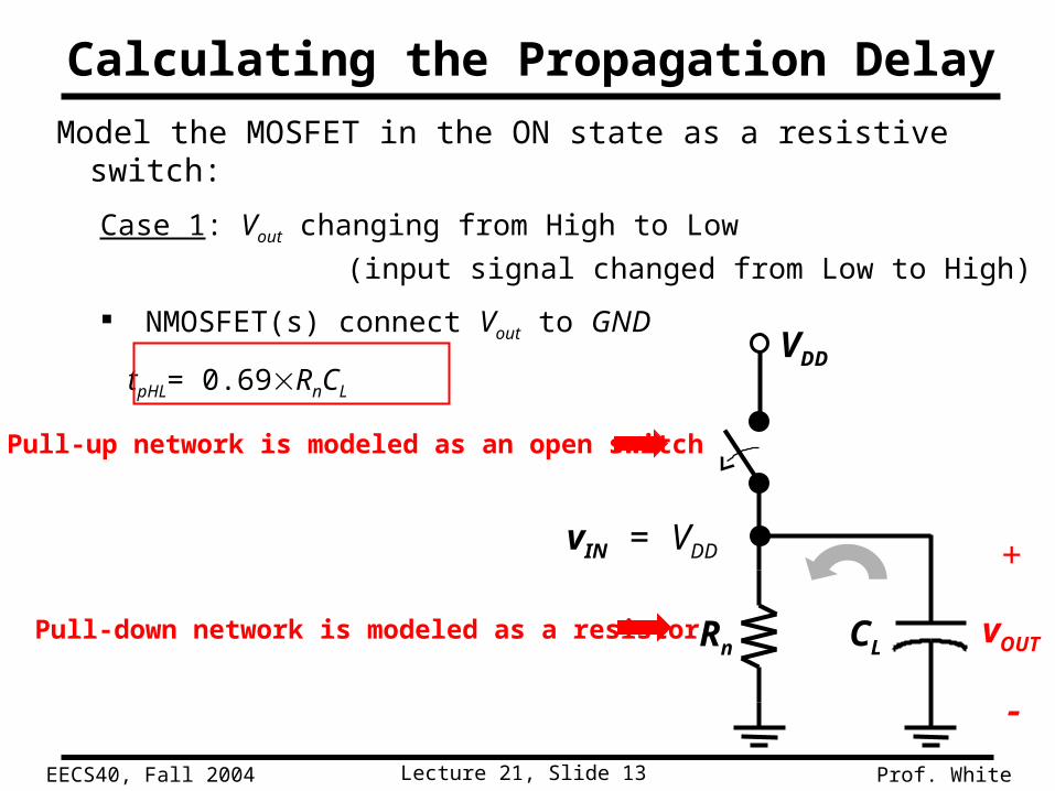
Model the MOSFET in the ON state as a resistive switch:
Case 1: Vout changing from High to Low
(input signal changed from Low to High)
NMOSFET(s) connect Vout to GND
tpHL= 0.69RnCL
Calculating the Propagation Delay
VDD
Pull-down network is modeled as a resistor
Pull-up network is modeled as an open switch
CL
+
vOUT
vIN = VDD
Rn
Lecture 21, Slide 14EECS40, Fall 2004 Prof. White
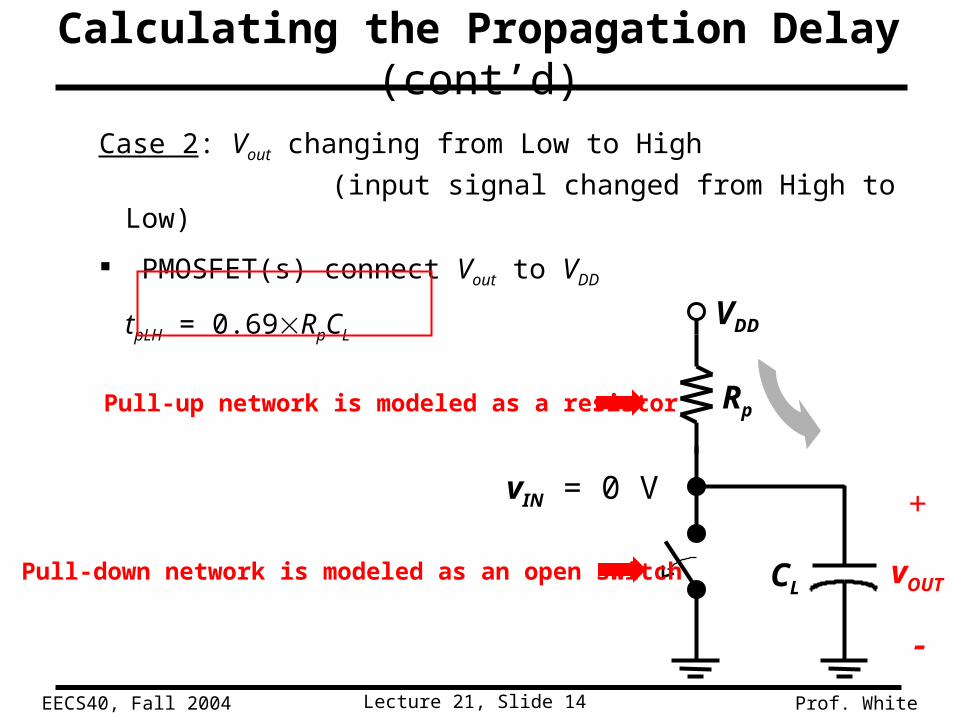
Calculating the Propagation Delay (cont’d)
Case 2: Vout changing from Low to High
(input signal changed from High to Low)
PMOSFET(s) connect Vout to VDD
tpLH = 0.69RpCLVDD
Rp
Pull-down network is modeled as an open switch
Pull-up network is modeled as a resistor
CL
+
vOUT
vIN = 0 V

Lecture 21, Slide 15EECS40, Fall 2004 Prof. White
Output Capacitance of a Logic Gate
• The output capacitance of a logic gate is comprised of several components:
• pn-junction and gate-drain capacitance– both NMOS and PMOS transistors
• capacitance of connecting wires• input capacitances of the fan-out gates
“extrinsiccapacitance”
“intrinsiccapacitance”
Impact of gate-drain capacitance
Lecture 21, Slide 16EECS40, Fall 2004 Prof. White
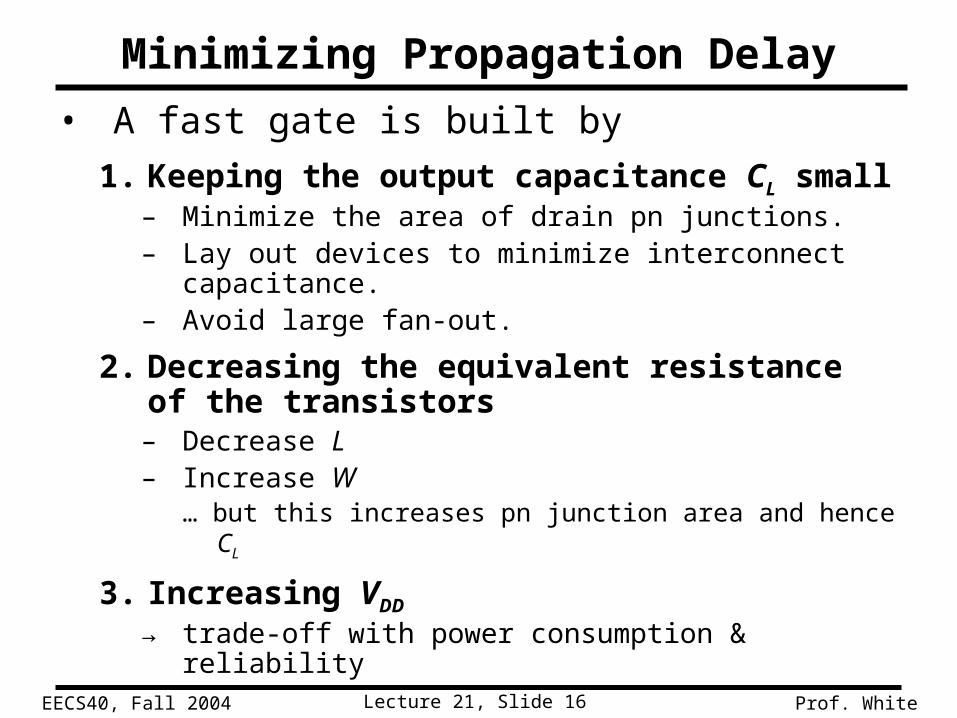
Minimizing Propagation Delay
• A fast gate is built by
1. Keeping the output capacitance CL small– Minimize the area of drain pn junctions.– Lay out devices to minimize interconnect
capacitance.– Avoid large fan-out.
2. Decreasing the equivalent resistance of the transistors– Decrease L– Increase W
… but this increases pn junction area and hence CL
3. Increasing VDD
→ trade-off with power consumption & reliability
Lecture 21, Slide 17EECS40, Fall 2004 Prof. White
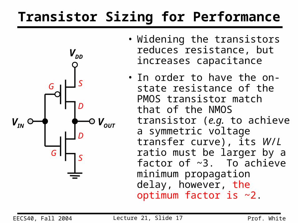
Transistor Sizing for Performance
• Widening the transistors reduces resistance, but increases capacitance
• In order to have the on-state resistance of the PMOS transistor match that of the NMOS transistor (e.g. to achieve a symmetric voltage transfer curve), its W/L ratio must be larger by a factor of ~3. To achieve minimum propagation delay, however, the optimum factor is ~2.
VDD
VIN VOUT
S
D
G
GS
D
Lecture 21, Slide 18EECS40, Fall 2004 Prof. White
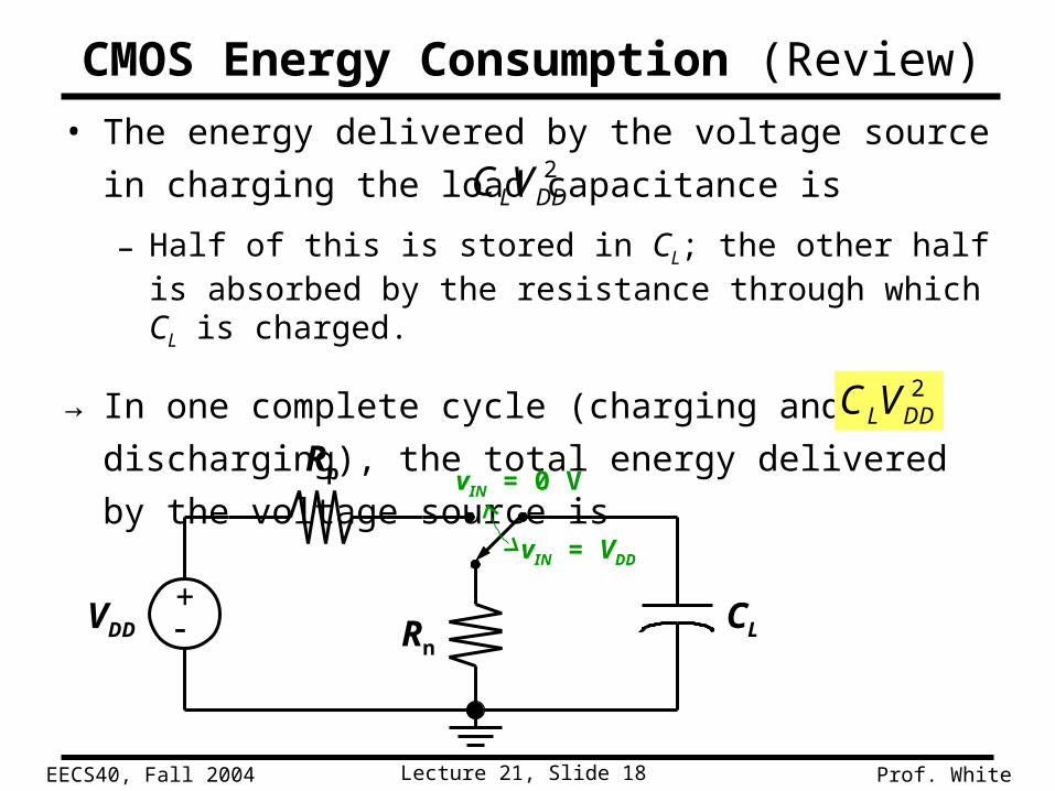
CMOS Energy Consumption (Review)
• The energy delivered by the voltage source in charging
the load capacitance is
– Half of this is stored in CL; the other half is absorbed by the resistance through which CL is charged.
→In one complete cycle (charging and discharging), the
total energy delivered by the voltage source is
RnVDD
+ CL
Rp
2DDLVC
2DDLVC
vIN = 0 V
vIN = VDD
Lecture 21, Slide 19EECS40, Fall 2004 Prof. White
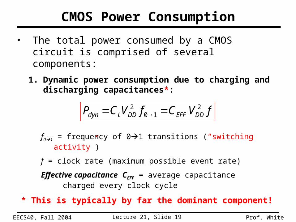
CMOS Power Consumption
• The total power consumed by a CMOS circuit is comprised of several components:
1. Dynamic power consumption due to charging and discharging capacitances*:
f01 = frequency of 01 transitions (“switching activity”)
f = clock rate (maximum possible event rate)
Effective capacitance CEFF = average capacitance charged every
clock cycle
* This is typically by far the dominant component!
fVCfVCP DDEFFDDLdyn2
102
Lecture 21, Slide 20EECS40, Fall 2004 Prof. White
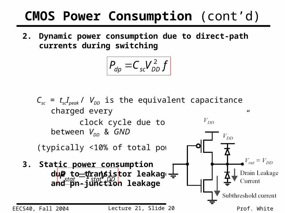
CMOS Power Consumption (cont’d)
2. Dynamic power consumption due to direct-path currents during switching
Csc = tscIpeak / VDD is the equivalent capacitance charged every
clock cycle due to “short-circuits” between VDD & GND
(typically <10% of total power consumption)
3. Static power consumption due to transistor leakage and pn-junction leakage
fVCP DDscdp2
DDstatstat VIP

Lecture 21, Slide 21EECS40, Fall 2004 Prof. White
Low-Power Design Techniques
1. Reduce VDD
→ quadratic effect on Pdyn
Example: Reducing VDD from 2.5 V to 1.25 V reduces power dissipation by factor of 4
– Lower bound is set by VT: VDD should be >2VT
2. Reduce load capacitance→ Use minimum-sized transistors whenever possible
3. Reduce the switching activity– involves design considerations at the architecture
level (beyond the scope of this class!)
Lecture 21, Slide 22EECS40, Fall 2004 Prof. White
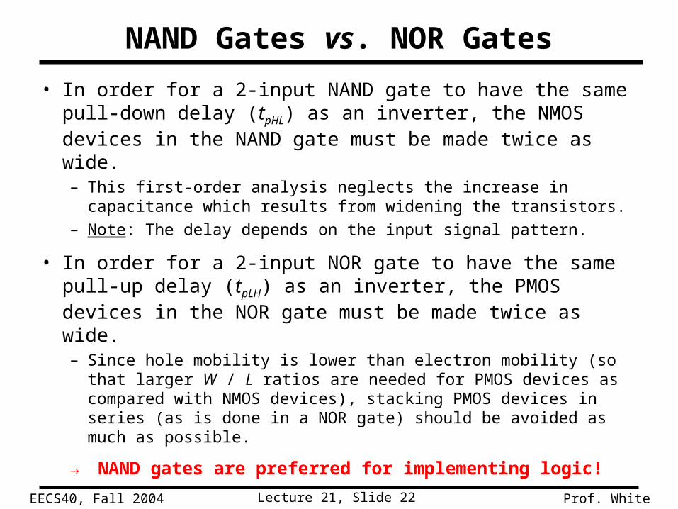
NAND Gates vs. NOR Gates
• In order for a 2-input NAND gate to have the same pull-down delay (tpHL) as an inverter, the NMOS devices in the NAND gate must be made twice as wide.– This first-order analysis neglects the increase in capacitance
which results from widening the transistors. – Note: The delay depends on the input signal pattern.
• In order for a 2-input NOR gate to have the same pull-up delay (tpLH) as an inverter, the PMOS devices in the NOR gate must be made twice as wide.– Since hole mobility is lower than electron mobility (so that larger
W / L ratios are needed for PMOS devices as compared with NMOS devices), stacking PMOS devices in series (as is done in a NOR gate) should be avoided as much as possible.
→ NAND gates are preferred for implementing logic!


![Sistem Berkas[sequential]](https://img.pdfslide.tips/doc/110x75/5571f97949795991698fa6ee/sistem-berkassequential.jpg)