Embed Size (px)
Citation preview
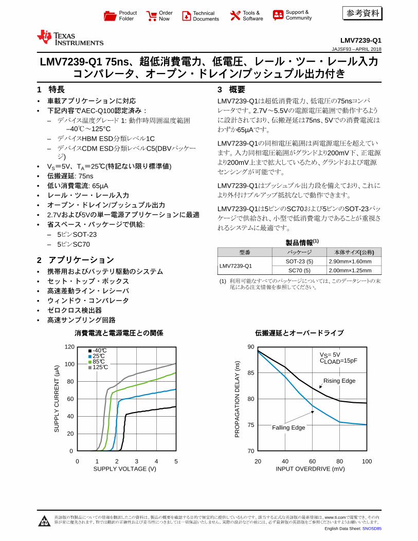
0 1 2 3 4 5
0
20
40
60
80
100
120
SU
PP
LY C
UR
RE
NT
(�
A)
SUPPLY VOLTAGE (V)
-40°C25°C85°C125°C
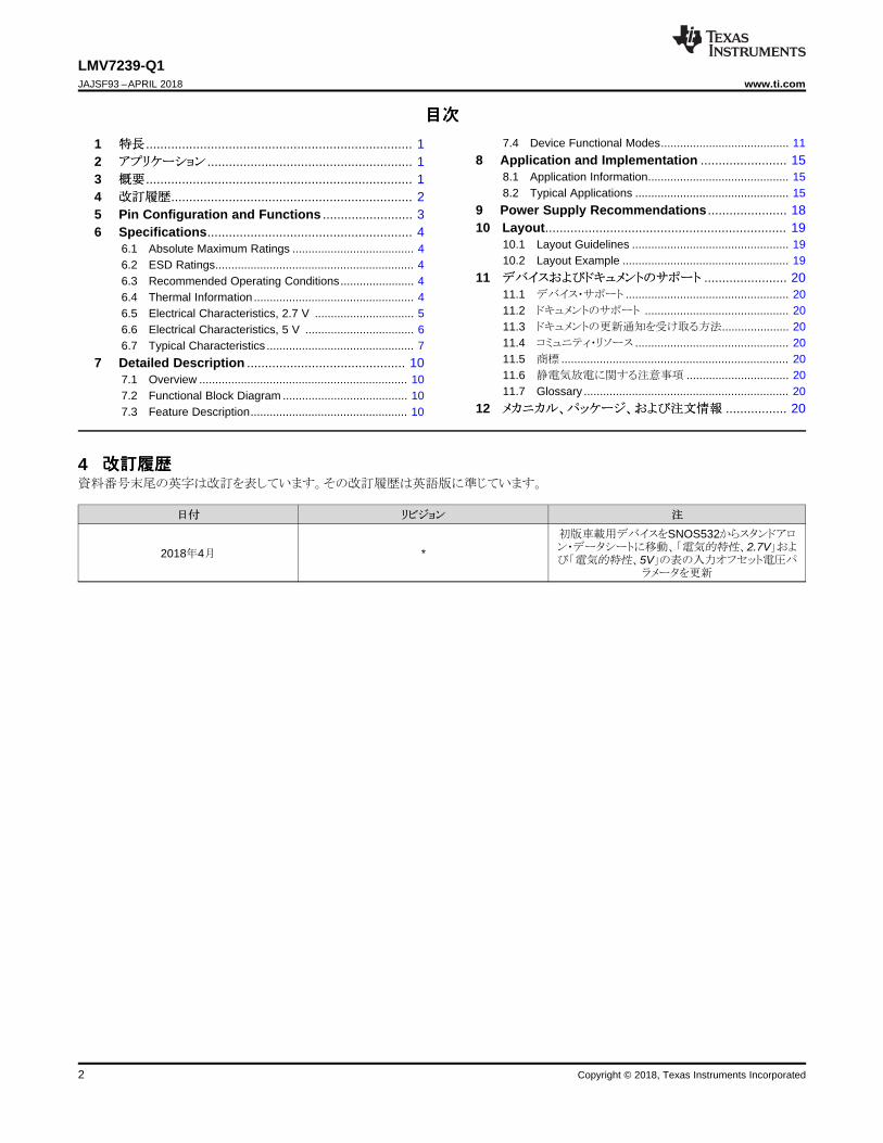
20 40 60 80 100
70
75
80
85
90
PR
OP
AG
AT
ION
DE
LAY
(ns
)
INPUT OVERDRIVE (mV)
Rising Edge
Falling Edge
VS= 5VCLOAD=15pF
Product
Folder
Order
Now
Technical
Documents
Tools &
Software
Support &Community
英語版のTI製品についての情報を翻訳したこの資料は、製品の概要を確認する目的で便宜的に提供しているものです。該当する正式な英語版の最新情報は、www.ti.comで閲覧でき、その内容が常に優先されます。TIでは翻訳の正確性および妥当性につきましては一切保証いたしません。実際の設計などの前には、必ず最新版の英語版をご参照くださいますようお願いいたします。
English Data Sheet: SNOSD85
LMV7239-Q1JAJSF93 –APRIL 2018
参参考考資資料料
LMV7239-Q1 75ns、、超超低低消消費費電電力力、、低低電電圧圧、、レレーールル・・ツツーー・・レレーールル入入力力ココンンパパレレーータタ、、オオーーププンン・・ドドレレイインン/ププッッシシュュププルル出出力力付付きき
1
1 特特長長1• 車載アプリケーションに対応• 下記内容でAEC-Q100認定済み:
– デバイス温度グレード 1: 動作時周囲温度範囲 –40℃~125°C
– デバイスHBM ESD分類レベル1C– デバイスCDM ESD分類レベルC5(DBVパッケー
ジ)• VS=5V、TA=25℃(特記ない限り標準値)• 伝搬遅延: 75ns• 低い消費電流: 65µA• レール・ツー・レール入力• オープン・ドレイン/プッシュプル出力• 2.7Vおよび5Vの単一電源アプリケーションに最適• 省スペース・パッケージで供給:
– 5ピンSOT-23– 5ピンSC70
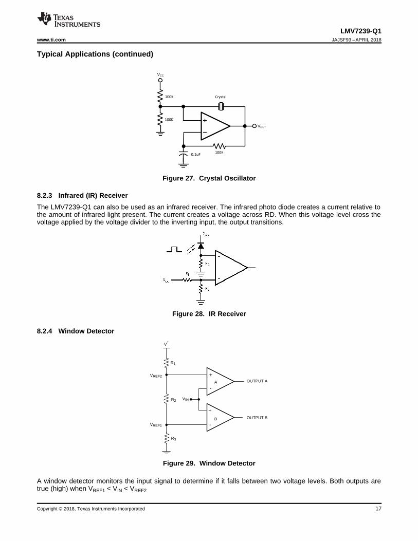
2 アアププリリケケーーシショョンン• 携帯用およびバッテリ駆動のシステム• セット・トップ・ボックス• 高速差動ライン・レシーバ• ウィンドウ・コンパレータ• ゼロクロス検出器• 高速サンプリング回路
3 概概要要LMV7239-Q1は超低消費電力、低電圧の75nsコンパ
レータです。2.7V~5.5Vの電源電圧範囲で動作するよう
に設計されており、伝搬遅延は75ns、5Vでの消費電流は
わずか65µAです。
LMV7239-Q1の同相電圧範囲は両電源電圧を超えてい
ます。入力同相電圧範囲がグランドより200mV下、正電源
より200mV上まで拡大しているため、グランドおよび電源
センシングが可能です。
LMV7239-Q1はプッシュプル出力段を備えており、これに
より外付けプルアップ抵抗なしで動作できます。
LMV7239-Q1は5ピンのSC70および5ピンのSOT-23パッ
ケージで供給され、小型で低消費電力であることが重視さ
れるシステムに最適です。
製製品品情情報報(1)
型型番番 パパッッケケーージジ 本本体体ササイイズズ(公公称称)
LMV7239-Q1SOT-23 (5) 2.90mm×1.60mmSC70 (5) 2.00mm×1.25mm
(1) 利用可能なすべてのパッケージについては、このデータシートの末尾にある注文情報を参照してください。
消消費費電電流流とと電電源源電電圧圧ととのの関関係係 伝伝搬搬遅遅延延ととオオーーババーードドラライイブブ
2
LMV7239-Q1JAJSF93 –APRIL 2018 www.ti.com
Copyright © 2018, Texas Instruments Incorporated
目目次次1 特特長長.......................................................................... 12 アアププリリケケーーシショョンン ......................................................... 13 概概要要.......................................................................... 14 改改訂訂履履歴歴................................................................... 25 Pin Configuration and Functions ......................... 36 Specifications......................................................... 4
6.1 Absolute Maximum Ratings ...................................... 46.2 ESD Ratings.............................................................. 46.3 Recommended Operating Conditions....................... 46.4 Thermal Information .................................................. 46.5 Electrical Characteristics, 2.7 V ............................... 56.6 Electrical Characteristics, 5 V .................................. 66.7 Typical Characteristics .............................................. 7
7 Detailed Description ............................................ 107.1 Overview ................................................................. 107.2 Functional Block Diagram ....................................... 107.3 Feature Description................................................. 10
7.4 Device Functional Modes........................................ 118 Application and Implementation ........................ 15
8.1 Application Information............................................ 158.2 Typical Applications ................................................ 15
9 Power Supply Recommendations ...................... 1810 Layout................................................................... 19
10.1 Layout Guidelines ................................................. 1910.2 Layout Example .................................................... 19
11 デデババイイススおおよよびびドドキキュュメメンントトののササポポーートト ....................... 2011.1 デバイス・サポート ................................................... 2011.2 ドキュメントのサポート ............................................. 2011.3 ドキュメントの更新通知を受け取る方法..................... 2011.4 コミュニティ・リソース ................................................ 2011.5 商標 ....................................................................... 2011.6 静電気放電に関する注意事項 ................................ 2011.7 Glossary ................................................................ 20
12 メメカカニニカカルル、、パパッッケケーージジ、、おおよよびび注注文文情情報報 ................. 20
4 改改訂訂履履歴歴資料番号末尾の英字は改訂を表しています。その改訂履歴は英語版に準じています。
日日付付 リリビビジジョョンン 注注
2018年4月 *
初版車載用デバイスをSNOS532からスタンドアロン・データシートに移動、「電気的特性、2.7V」および「電気的特性、5V」の表の入力オフセット電圧パ
ラメータを更新
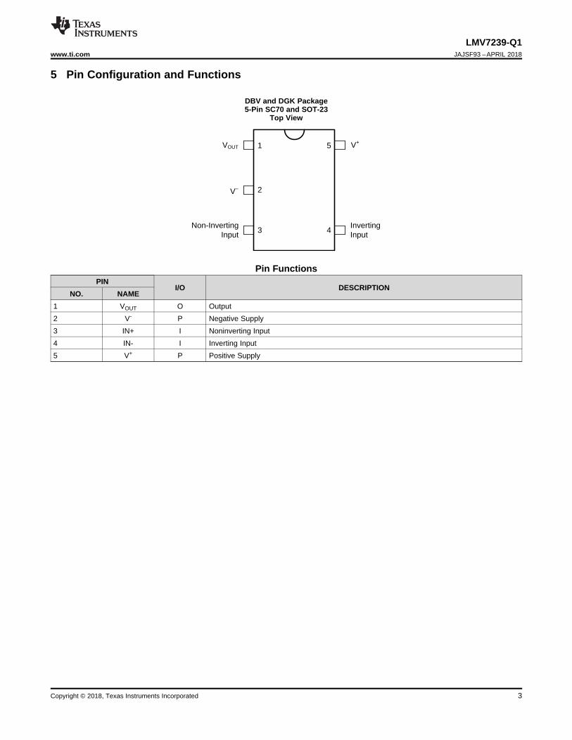
Inverting Input
5 V+
V±
VOUT
Non-Inverting Input
4
1
2
3
3
LMV7239-Q1www.ti.com JAJSF93 –APRIL 2018
Copyright © 2018, Texas Instruments Incorporated
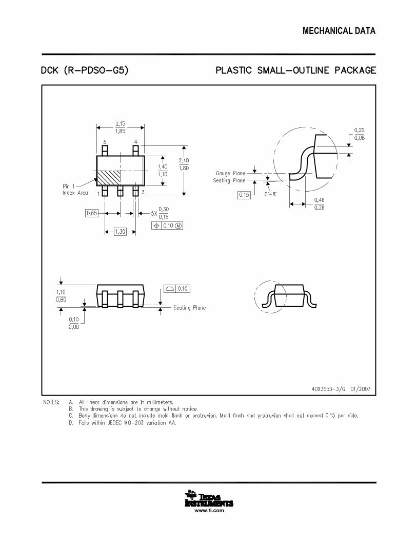
5 Pin Configuration and Functions
DBV and DGK Package5-Pin SC70 and SOT-23
Top View
Pin FunctionsPIN
I/O DESCRIPTIONNO. NAME
1 VOUT O Output2 V- P Negative Supply3 IN+ I Noninverting Input4 IN- I Inverting Input5 V+ P Positive Supply
4
LMV7239-Q1JAJSF93 –APRIL 2018 www.ti.com
Copyright © 2018, Texas Instruments Incorporated
(1) Stresses beyond those listed under absolute maximum ratings may cause permanent damage to the device. These are stress ratingsonly, and functional operation of the device at these or any other conditions beyond those indicated under recommended operatingconditions is not implied. Exposure to absolute-maximum-rated conditions for extended periods may affect device reliability.
(2) Applies to both single-supply and split-supply operation. Continuous short circuit operation at elevated ambient temperature can result inexceeding the maximum allowed junction temperature of 150°C. Output currents in excess of ±30mA over long term may adverselyaffect reliability.
(3) Limiting input pin current is only necessary for input voltages that exceed absolute maximum input voltage ratings.
6 Specifications
6.1 Absolute Maximum RatingsOver operating free-air temperature range (unless otherwise noted) (1)
MIN MAX UNITDifferential Input Voltage ± Supply Voltage VOutput Short Circuit Duration See (2)
Supply Voltage (V+ - V−) 6 VSOLDERING INFORMATION
Infrared or Convection (20 sec) 235 °CWave Soldering (10 sec) 260 (lead temp) °C
Voltage at Input/Output Pins (V+) +0.3, (V−) −0.3 VCurrent at Input Pin (3) ±10 mAStorage Temperature, Tstg –65 150 °CJunction Temperature,TJ 150 °C
(1) JEDEC document JEP157 states that 250-V CDM allows safe manufacturing with a standard ESD control process. Manufacturing withless than 250-V CDM is possible with the necessary precautions.
6.2 ESD RatingsVALUE UNIT
V(ESD)Electrostaticdischarge
Human-body model (HBM), per AEC Q100-002 (1) ±1000VCharged-device model (CDM), per AEC Q100-011 (1) DBV package only ±750
Machine model (MM) ±100
(1) The maximum power dissipation is a function of TJ(MAX), θJA. The maximum allowable power dissipation at any ambient temperature isPD = (TJ(MAX) – TA) / θJA. All numbers apply for packages soldered directly onto a PCB.
6.3 Recommended Operating ConditionsMIN MAX UNIT
Supply Voltages (V+ - V−) 2.7 5.5 VTemperature Range (1) –40 125 °C
(1) For more information about traditional and new thermal metrics, see the Semiconductor and IC Package Thermal Metrics applicationreport.
6.4 Thermal Information
THERMAL METRIC (1)LMV7239-Q1
UNITDGK (SC70) DBV (SOT-23)5 PINS 5 PINS
RθJA Junction-to-ambient thermal resistance 478 265 °C/W
5
LMV7239-Q1www.ti.com JAJSF93 –APRIL 2018
Copyright © 2018, Texas Instruments Incorporated
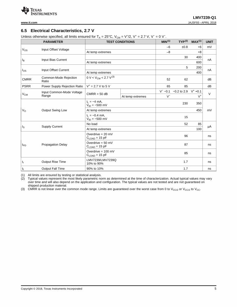
(1) All limits are ensured by testing or statistical analysis.(2) Typical values represent the most likely parametric norm as determined at the time of characterization. Actual typical values may vary
over time and will also depend on the application and configuration. The typical values are not tested and are not guaranteed onshipped production material.
(3) CMRR is not linear over the common mode range. Limits are guaranteed over the worst case from 0 to VCC/2 or VCC/2 to VCC.
6.5 Electrical Characteristics, 2.7 VUnless otherwise specified, all limits ensured for TA = 25°C, VCM = V+/2, V+ = 2.7 V, V− = 0 V−.
PARAMETER TEST CONDITIONS MIN (1) TYP (2) MAX (1) UNIT
VOS Input Offset Voltage–6 ±0.8 +6 mV
At temp extremes –8 +8
IB Input Bias Current30 400
nAAt temp extremes 600
IOS Input Offset Current5 200
nAAt temp extremes 400
CMRR Common-Mode RejectionRatio
0 V < VCM < 2.7 V (3)52 62 dB
PSRR Power Supply Rejection Ratio V+ = 2.7 V to 5 V 65 85 dB
VCMInput Common-Mode VoltageRange CMRR > 50 dB
V− −0.1 −0.2 to 2.9 V+ +0.1V
At temp extremes V− V+
VO Output Swing Low
IL = −4 mA,VID = −500 mV 230 350
mVAt temp extremes 450IL = −0.4 mA,VID = −500 mV 15
IS Supply CurrentNo load 52 85
µAAt temp extremes 100
tPD Propagation Delay
Overdrive = 20 mVCLOAD = 15 pF 96 ns
Overdrive = 50 mVCLOAD = 15 pF 87 ns
Overdrive = 100 mVCLOAD = 15 pF 85 ns
tr Output Rise Time LMV7239/LMV7239Q10% to 90% 1.7 ns
tf Output Fall Time 90% to 10% 1.7 ns
6
LMV7239-Q1JAJSF93 –APRIL 2018 www.ti.com
Copyright © 2018, Texas Instruments Incorporated
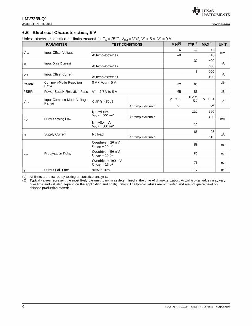
(1) All limits are ensured by testing or statistical analysis.(2) Typical values represent the most likely parametric norm as determined at the time of characterization. Actual typical values may vary
over time and will also depend on the application and configuration. The typical values are not tested and are not guaranteed onshipped production material.
6.6 Electrical Characteristics, 5 VUnless otherwise specified, all limits ensured for TA = 25°C, VCM = V+/2, V+ = 5 V, V− = 0 V.
PARAMETER TEST CONDITIONS MIN (1) TYP (2) MAX (1) UNIT
VOS Input Offset Voltage–6 ±1 +6
mVAt temp extremes –8 +8
IB Input Bias Current30 400
nAAt temp extremes 600
IOS Input Offset Current5 200
nAAt temp extremes 400
CMRR Common-Mode RejectionRatio
0 V < VCM < 5 V 52 67 dB
PSRR Power Supply Rejection Ratio V+ = 2.7 V to 5 V 65 85 dB
VCMInput Common-Mode VoltageRange CMRR > 50dB
V− −0.1 −0.2 to5.2 V+ +0.1
VAt temp extremes V− V+
VO Output Swing Low
IL = −4 mA,VID = −500 mV
230 350
mVAt temp extremes 450IL = −0.4 mA,VID = −500 mV 10
IS Supply Current No load65 95
µAAt temp extremes 110
tPD Propagation Delay
Overdrive = 20 mVCLOAD = 15 pF 89 ns
Overdrive = 50 mVCLOAD = 15 pF 82 ns
Overdrive = 100 mVCLOAD = 15 pF 75 ns
tf Output Fall Time 90% to 10% 1.2 ns
5-0.2 1 2 3 4-50
-40
-30
-20
-10
0
10
20
30
40
50
INP
UT
BIA
S C
UR
RE
NT
(nA
)
VIN (V)
VS = 5V
IBIAS+
IBIAS-
.01 .1 1 10
OUTPUT VOLTAGE REFERENCED TO GND (V)
.1
1
10
100
I SIN
K (
mA
)
VS = 2.7V
OUTPUT VOLTAGE REFERENCED TO V+ (V)
.01 .1 1 10.1
1
10
100
I SO
UR
CE (
mA
)
VS = 2.7V
.01 .1 1 10
OUTPUT VOLTAGE REFERENCED TO GND (V)
.1
1
10
100
I SIN
K (
mA
)
VS = 5V
10
OUTPUT VOLTAGE REFERENCED TO V+ (V)
.01 .1 1.1
1
10
100
I SO
UR
CE (
mA
)
VS = 5V
0 1 2 3 4 5
0
20
40
60
80
100
120
SU
PP
LY C
UR
RE
NT
(�
A)
SUPPLY VOLTAGE (V)
-40°C25°C85°C125°C
7
LMV7239-Q1www.ti.com JAJSF93 –APRIL 2018
Copyright © 2018, Texas Instruments Incorporated
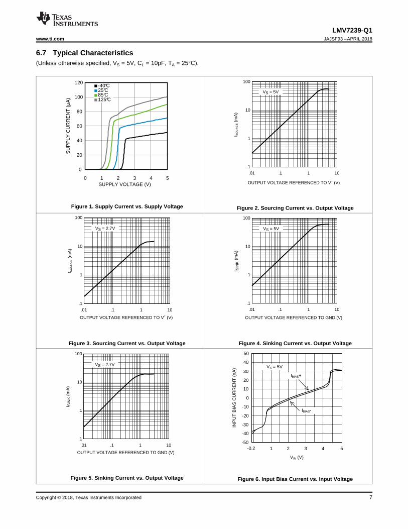
6.7 Typical Characteristics(Unless otherwise specified, VS = 5V, CL = 10pF, TA = 25°C).
Figure 1. Supply Current vs. Supply Voltage Figure 2. Sourcing Current vs. Output Voltage
Figure 3. Sourcing Current vs. Output Voltage Figure 4. Sinking Current vs. Output Voltage
Figure 5. Sinking Current vs. Output Voltage Figure 6. Input Bias Current vs. Input Voltage
0 20 40 60 80 100
88
90
92
94
96
PR
OP
AG
AT
ION
DE
LAY
(ns
)
CAPACITANCE (pF)
Rising Edge
Falling Edge
VS= 5VVOD=20mV
20 30 40 50 60 70 80 90 100
80
85
90
95
100
PR
OP
AG
AT
ION
DE
LAY
(ns
)
INPUT OVERDRIVE (mV)
Rising Edge
Falling Edge
VS= 2.7VCLOAD=15pF
-40 -20 0 20 40 60 80 100 120 140
80
90
100
110
120
130
140
PR
OP
AG
AT
ION
DE
LAY
(ns
)
TEMPERATURE (°C)
VS=5VVOD=20mVCLOAD=15pF
Falling Edge
Rising Edge
0 20 40 60 80 100
94
96
98
100
102
104
106
PR
OP
AG
AT
ION
DE
LAY
(ns
)
CAPACITANCE (pF)
Rising Edge
Falling Edge
VS= 2.7VVOD=20mV
0 1 2
-50
-40
-30
-20-10
0
10
2030
50
INP
UT
BIA
S C
UR
RE
NT
(nA
)
VIN (V)
2.7
VS = 2.7V
IBIAS-
IBIAS+
60
-60
70
40
-40 -20 0 20 40 60 80 100 120 140
80
90
100
110
120
130
140
150
160
PR
OP
AG
AT
ION
DE
LAY
(ns
)
TEMPERATURE (°C)
VS=2.7VVOD=20mVCLOAD=15pF
Falling Edge
Rising Edge
8
LMV7239-Q1JAJSF93 –APRIL 2018 www.ti.com
Copyright © 2018, Texas Instruments Incorporated
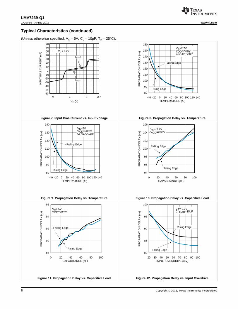
Typical Characteristics (continued)(Unless otherwise specified, VS = 5V, CL = 10pF, TA = 25°C).
Figure 7. Input Bias Current vs. Input Voltage Figure 8. Propagation Delay vs. Temperature
Figure 9. Propagation Delay vs. Temperature Figure 10. Propagation Delay vs. Capacitive Load
Figure 11. Propagation Delay vs. Capacitive Load Figure 12. Propagation Delay vs. Input Overdrive
0 1 2 3 4 5
80
90
100
110
PR
OP
AG
AT
ION
DE
LAY
(ns
)
INPUT COMMON MODE VOLTAGE (V)
Rising Edge
Falling Edge
VS= 5VVOD=20mVCLOAD=15pF
20 40 60 80 100
70
75
80
85
90P
RO
PA
GA
TIO
N D
ELA
Y (
ns)
INPUT OVERDRIVE (mV)
Rising Edge
Falling Edge
VS= 5VCLOAD=15pF
0.0 0.5 1.0 1.5 2.0 2.5 3.0
80
85
90
95
100
105
110
115
120
PR
OP
AG
AT
ION
DE
LAY
(ns
)
INPUT COMMON MODE VOLTAGE (V)
Rising Edge Falling Edge
VS= 2.7VVOD=20mVCLOAD=15pF
9
LMV7239-Q1www.ti.com JAJSF93 –APRIL 2018
Copyright © 2018, Texas Instruments Incorporated
Typical Characteristics (continued)(Unless otherwise specified, VS = 5V, CL = 10pF, TA = 25°C).
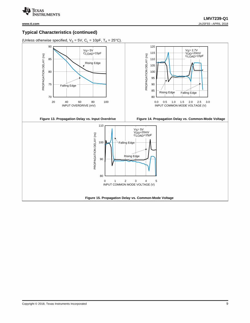
Figure 13. Propagation Delay vs. Input Overdrive Figure 14. Propagation Delay vs. Common-Mode Voltage
Figure 15. Propagation Delay vs. Common-Mode Voltage
10
LMV7239-Q1JAJSF93 –APRIL 2018 www.ti.com
Copyright © 2018, Texas Instruments Incorporated
7 Detailed Description
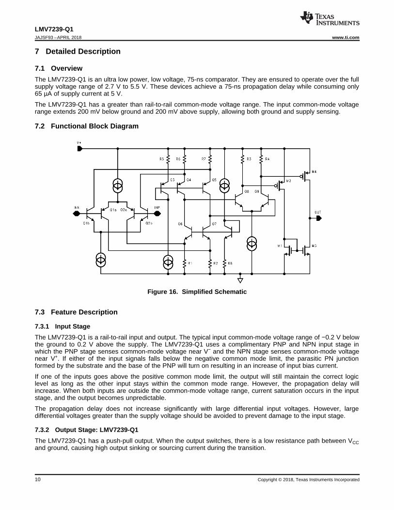
7.1 OverviewThe LMV7239-Q1 is an ultra low power, low voltage, 75-ns comparator. They are ensured to operate over the fullsupply voltage range of 2.7 V to 5.5 V. These devices achieve a 75-ns propagation delay while consuming only65 µA of supply current at 5 V.
The LMV7239-Q1 has a greater than rail-to-rail common-mode voltage range. The input common-mode voltagerange extends 200 mV below ground and 200 mV above supply, allowing both ground and supply sensing.
7.2 Functional Block Diagram
Figure 16. Simplified Schematic
7.3 Feature Description
7.3.1 Input StageThe LMV7239-Q1 is a rail-to-rail input and output. The typical input common-mode voltage range of −0.2 V belowthe ground to 0.2 V above the supply. The LMV7239-Q1 uses a complimentary PNP and NPN input stage inwhich the PNP stage senses common-mode voltage near V− and the NPN stage senses common-mode voltagenear V+. If either of the input signals falls below the negative common mode limit, the parasitic PN junctionformed by the substrate and the base of the PNP will turn on resulting in an increase of input bias current.
If one of the inputs goes above the positive common mode limit, the output will still maintain the correct logiclevel as long as the other input stays within the common mode range. However, the propagation delay willincrease. When both inputs are outside the common-mode voltage range, current saturation occurs in the inputstage, and the output becomes unpredictable.
The propagation delay does not increase significantly with large differential input voltages. However, largedifferential voltages greater than the supply voltage should be avoided to prevent damage to the input stage.
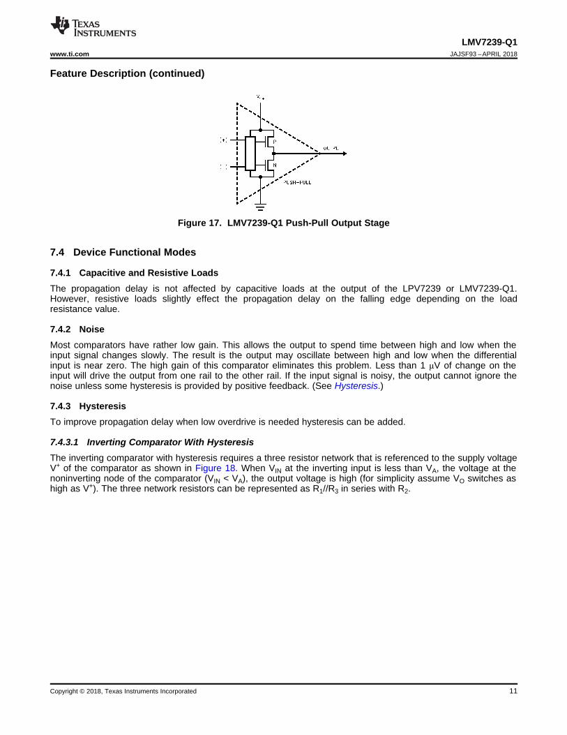
7.3.2 Output Stage: LMV7239-Q1The LMV7239-Q1 has a push-pull output. When the output switches, there is a low resistance path between VCCand ground, causing high output sinking or sourcing current during the transition.
11
LMV7239-Q1www.ti.com JAJSF93 –APRIL 2018
Copyright © 2018, Texas Instruments Incorporated
Feature Description (continued)
Figure 17. LMV7239-Q1 Push-Pull Output Stage
7.4 Device Functional Modes
7.4.1 Capacitive and Resistive LoadsThe propagation delay is not affected by capacitive loads at the output of the LPV7239 or LMV7239-Q1.However, resistive loads slightly effect the propagation delay on the falling edge depending on the loadresistance value.
7.4.2 NoiseMost comparators have rather low gain. This allows the output to spend time between high and low when theinput signal changes slowly. The result is the output may oscillate between high and low when the differentialinput is near zero. The high gain of this comparator eliminates this problem. Less than 1 μV of change on theinput will drive the output from one rail to the other rail. If the input signal is noisy, the output cannot ignore thenoise unless some hysteresis is provided by positive feedback. (See Hysteresis.)
7.4.3 HysteresisTo improve propagation delay when low overdrive is needed hysteresis can be added.
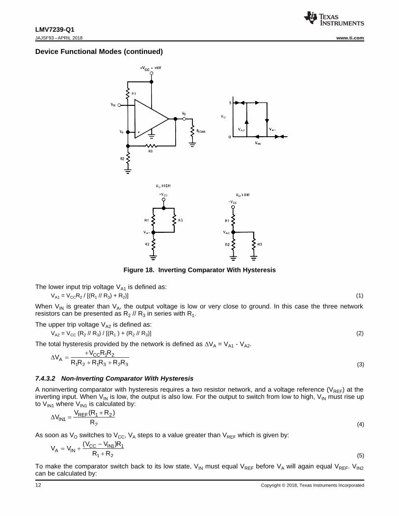
7.4.3.1 Inverting Comparator With HysteresisThe inverting comparator with hysteresis requires a three resistor network that is referenced to the supply voltageV+ of the comparator as shown in Figure 18. When VIN at the inverting input is less than VA, the voltage at thenoninverting node of the comparator (VIN < VA), the output voltage is high (for simplicity assume VO switches ashigh as V+). The three network resistors can be represented as R1//R3 in series with R2.
CC IN1 1A IN
1 2
(V V )RV V
R R
� �
�
REF 1 2IN1
2
V (R R )V
R
�'
CC 1 2A
1 2 1 3 2 3
V R RV
R R R R R R
�'
� �
12
LMV7239-Q1JAJSF93 –APRIL 2018 www.ti.com
Copyright © 2018, Texas Instruments Incorporated
Device Functional Modes (continued)
Figure 18. Inverting Comparator With Hysteresis
The lower input trip voltage VA1 is defined as:VA1 = VCCR2 / [(R1 // R3) + R2)] (1)
When VIN is greater than VA, the output voltage is low or very close to ground. In this case the three networkresistors can be presented as R2 // R3 in series with R1.
The upper trip voltage VA2 is defined as:VA2 = VCC (R2 // R3) / [(R1 ) + (R2 // R3)] (2)
The total hysteresis provided by the network is defined as ΔVA = VA1 - VA2.
(3)
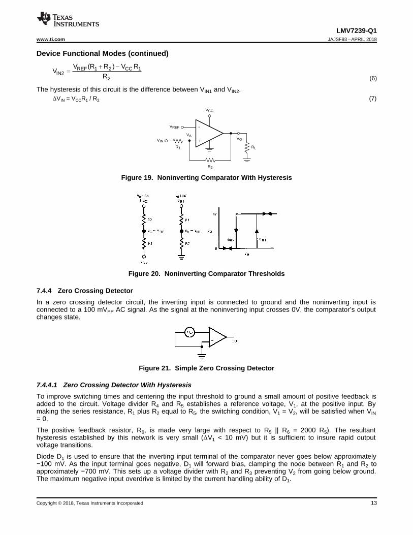
7.4.3.2 Non-Inverting Comparator With HysteresisA noninverting comparator with hysteresis requires a two resistor network, and a voltage reference (VREF) at theinverting input. When VIN is low, the output is also low. For the output to switch from low to high, VIN must rise upto VIN1 where VIN1 is calculated by:
(4)
As soon as VO switches to VCC, VA steps to a value greater than VREF which is given by:
(5)
To make the comparator switch back to its low state, VIN must equal VREF before VA will again equal VREF. VIN2can be calculated by:
VCC
VO
R2
R1
VA
+
-VREF
RL
VIN
REF 1 2 CC 1IN2
2
V (R R ) V RV
R
� �
13
LMV7239-Q1www.ti.com JAJSF93 –APRIL 2018
Copyright © 2018, Texas Instruments Incorporated
Device Functional Modes (continued)
(6)
The hysteresis of this circuit is the difference between VIN1 and VIN2.ΔVIN = VCCR1 / R2 (7)
Figure 19. Noninverting Comparator With Hysteresis
Figure 20. Noninverting Comparator Thresholds
7.4.4 Zero Crossing DetectorIn a zero crossing detector circuit, the inverting input is connected to ground and the noninverting input isconnected to a 100 mVPP AC signal. As the signal at the noninverting input crosses 0V, the comparator’s outputchanges state.
Figure 21. Simple Zero Crossing Detector
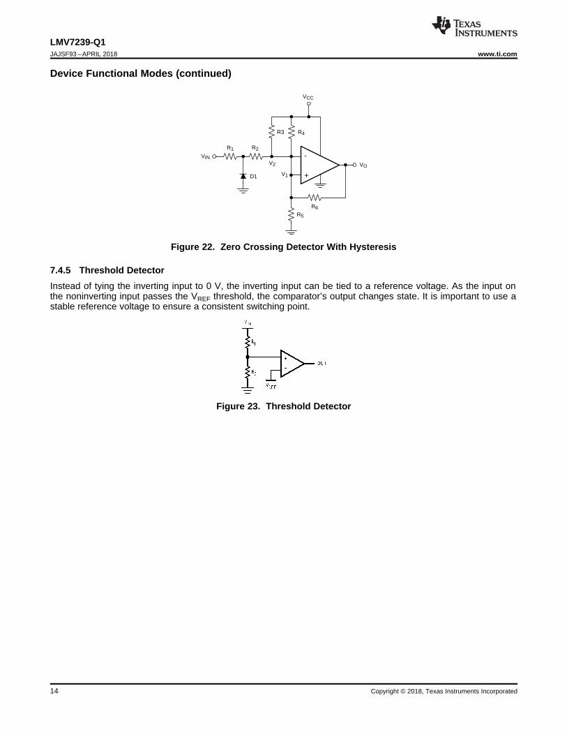
7.4.4.1 Zero Crossing Detector With HysteresisTo improve switching times and centering the input threshold to ground a small amount of positive feedback isadded to the circuit. Voltage divider R4 and R5 establishes a reference voltage, V1, at the positive input. Bymaking the series resistance, R1 plus R2 equal to R5, the switching condition, V1 = V2, will be satisfied when VIN= 0.
The positive feedback resistor, R6, is made very large with respect to R5 || R6 = 2000 R5). The resultanthysteresis established by this network is very small (ΔV1 < 10 mV) but it is sufficient to insure rapid outputvoltage transitions.
Diode D1 is used to ensure that the inverting input terminal of the comparator never goes below approximately−100 mV. As the input terminal goes negative, D1 will forward bias, clamping the node between R1 and R2 toapproximately −700 mV. This sets up a voltage divider with R2 and R3 preventing V2 from going below ground.The maximum negative input overdrive is limited by the current handling ability of D1.
R2
R4
VO
R5
R6
R3
V2
+
-R1
VIN
D1
VCC
V1
14
LMV7239-Q1JAJSF93 –APRIL 2018 www.ti.com
Copyright © 2018, Texas Instruments Incorporated
Device Functional Modes (continued)
Figure 22. Zero Crossing Detector With Hysteresis
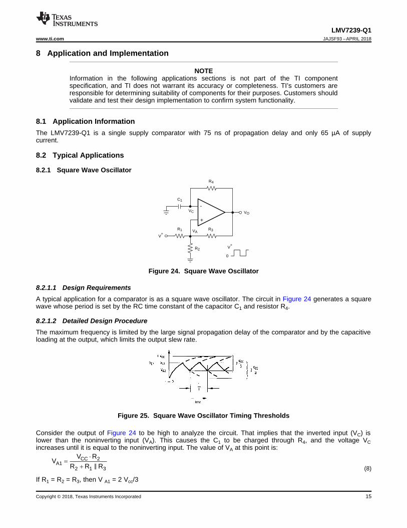
7.4.5 Threshold DetectorInstead of tying the inverting input to 0 V, the inverting input can be tied to a reference voltage. As the input onthe noninverting input passes the VREF threshold, the comparator’s output changes state. It is important to use astable reference voltage to ensure a consistent switching point.
Figure 23. Threshold Detector
CC 2A1
2 1 3
V RV
R R R
�
� R
C1
R4
VO
R2
R3R1 VA
+
-VC
V+
0
V+
15
LMV7239-Q1www.ti.com JAJSF93 –APRIL 2018
Copyright © 2018, Texas Instruments Incorporated
8 Application and Implementation
NOTEInformation in the following applications sections is not part of the TI componentspecification, and TI does not warrant its accuracy or completeness. TI’s customers areresponsible for determining suitability of components for their purposes. Customers shouldvalidate and test their design implementation to confirm system functionality.
8.1 Application InformationThe LMV7239-Q1 is a single supply comparator with 75 ns of propagation delay and only 65 µA of supplycurrent.
8.2 Typical Applications
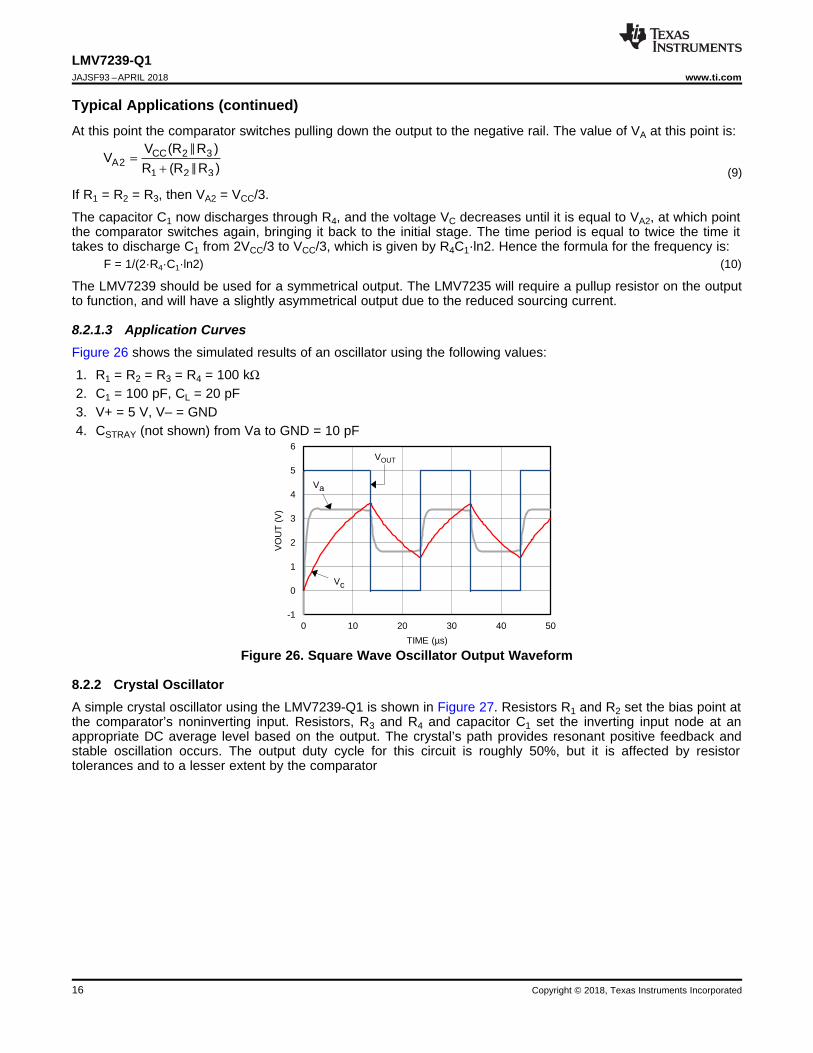
8.2.1 Square Wave Oscillator
Figure 24. Square Wave Oscillator
8.2.1.1 Design RequirementsA typical application for a comparator is as a square wave oscillator. The circuit in Figure 24 generates a squarewave whose period is set by the RC time constant of the capacitor C1 and resistor R4.
8.2.1.2 Detailed Design ProcedureThe maximum frequency is limited by the large signal propagation delay of the comparator and by the capacitiveloading at the output, which limits the output slew rate.
Figure 25. Square Wave Oscillator Timing Thresholds
Consider the output of Figure 24 to be high to analyze the circuit. That implies that the inverted input (VC) islower than the noninverting input (VA). This causes the C1 to be charged through R4, and the voltage VCincreases until it is equal to the noninverting input. The value of VA at this point is:
(8)
If R1 = R2 = R3, then V A1 = 2 Vcc/3
-1
0
1
2
3
4
5
6
0 10 20 30 40 50
VO
UT
(V
)
TIME (µs) C001
VOUT
Va
Vc
CC 2 3A2
1 2 3
V (R R )V
R (R R )
�
R
R
16
LMV7239-Q1JAJSF93 –APRIL 2018 www.ti.com
Copyright © 2018, Texas Instruments Incorporated
Typical Applications (continued)At this point the comparator switches pulling down the output to the negative rail. The value of VA at this point is:
(9)
If R1 = R2 = R3, then VA2 = VCC/3.
The capacitor C1 now discharges through R4, and the voltage VC decreases until it is equal to VA2, at which pointthe comparator switches again, bringing it back to the initial stage. The time period is equal to twice the time ittakes to discharge C1 from 2VCC/3 to VCC/3, which is given by R4C1·ln2. Hence the formula for the frequency is:
F = 1/(2·R4·C1·ln2) (10)
The LMV7239 should be used for a symmetrical output. The LMV7235 will require a pullup resistor on the outputto function, and will have a slightly asymmetrical output due to the reduced sourcing current.
8.2.1.3 Application CurvesFigure 26 shows the simulated results of an oscillator using the following values:
1. R1 = R2 = R3 = R4 = 100 kΩ2. C1 = 100 pF, CL = 20 pF3. V+ = 5 V, V– = GND4. CSTRAY (not shown) from Va to GND = 10 pF
Figure 26. Square Wave Oscillator Output Waveform
8.2.2 Crystal OscillatorA simple crystal oscillator using the LMV7239-Q1 is shown in Figure 27. Resistors R1 and R2 set the bias point atthe comparator’s noninverting input. Resistors, R3 and R4 and capacitor C1 set the inverting input node at anappropriate DC average level based on the output. The crystal’s path provides resonant positive feedback andstable oscillation occurs. The output duty cycle for this circuit is roughly 50%, but it is affected by resistortolerances and to a lesser extent by the comparator
V+
R1
R2
R3
-
+
-
+OUTPUT A
OUTPUT B
VREF2
VREF1
A
B
VIN
Crystal100K
VOUT
0.1uF
VCC
100K
100K
17
LMV7239-Q1www.ti.com JAJSF93 –APRIL 2018
Copyright © 2018, Texas Instruments Incorporated
Typical Applications (continued)
Figure 27. Crystal Oscillator
8.2.3 Infrared (IR) ReceiverThe LMV7239-Q1 can also be used as an infrared receiver. The infrared photo diode creates a current relative tothe amount of infrared light present. The current creates a voltage across RD. When this voltage level cross thevoltage applied by the voltage divider to the inverting input, the output transitions.
Figure 28. IR Receiver
8.2.4 Window Detector
Figure 29. Window Detector
A window detector monitors the input signal to determine if it falls between two voltage levels. Both outputs aretrue (high) when VREF1 < VIN < VREF2
V+
VREF2
VREF1
BOTH OUTPUTS ARE HIGH
OUTPUT A
OUTPUT BVIN
18
LMV7239-Q1JAJSF93 –APRIL 2018 www.ti.com
Copyright © 2018, Texas Instruments Incorporated
Typical Applications (continued)
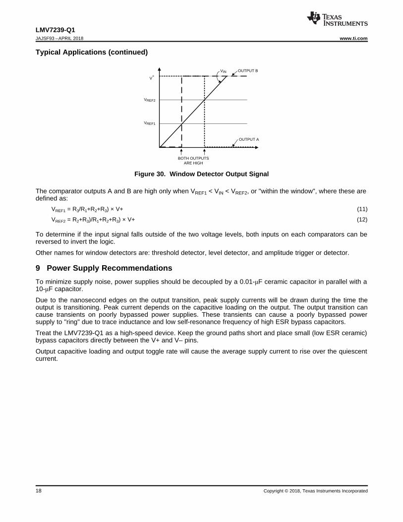
Figure 30. Window Detector Output Signal
The comparator outputs A and B are high only when VREF1 < VIN < VREF2, or "within the window", where these aredefined as:
VREF1 = R3/R1+R2+R3) × V+ (11)
VREF2 = R2+R3)/R1+R2+R3) × V+ (12)
To determine if the input signal falls outside of the two voltage levels, both inputs on each comparators can bereversed to invert the logic.
Other names for window detectors are: threshold detector, level detector, and amplitude trigger or detector.
9 Power Supply RecommendationsTo minimize supply noise, power supplies should be decoupled by a 0.01-μF ceramic capacitor in parallel with a10-μF capacitor.
Due to the nanosecond edges on the output transition, peak supply currents will be drawn during the time theoutput is transitioning. Peak current depends on the capacitive loading on the output. The output transition cancause transients on poorly bypassed power supplies. These transients can cause a poorly bypassed powersupply to "ring" due to trace inductance and low self-resonance frequency of high ESR bypass capacitors.
Treat the LMV7239-Q1 as a high-speed device. Keep the ground paths short and place small (low ESR ceramic)bypass capacitors directly between the V+ and V– pins.
Output capacitive loading and output toggle rate will cause the average supply current to rise over the quiescentcurrent.
19
LMV7239-Q1www.tij.co.jp JAJSF93 –APRIL 2018
Copyright © 2018, Texas Instruments Incorporated
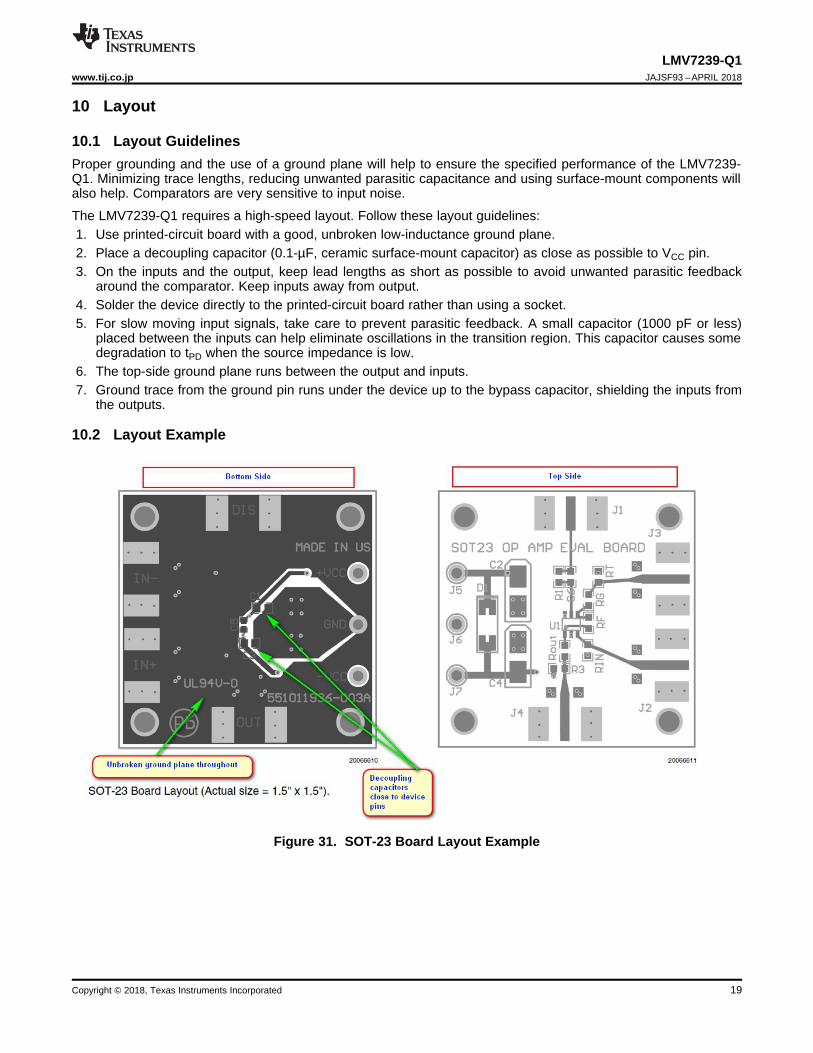
10 Layout
10.1 Layout GuidelinesProper grounding and the use of a ground plane will help to ensure the specified performance of the LMV7239-Q1. Minimizing trace lengths, reducing unwanted parasitic capacitance and using surface-mount components willalso help. Comparators are very sensitive to input noise.
The LMV7239-Q1 requires a high-speed layout. Follow these layout guidelines:1. Use printed-circuit board with a good, unbroken low-inductance ground plane.2. Place a decoupling capacitor (0.1-µF, ceramic surface-mount capacitor) as close as possible to VCC pin.3. On the inputs and the output, keep lead lengths as short as possible to avoid unwanted parasitic feedback
around the comparator. Keep inputs away from output.4. Solder the device directly to the printed-circuit board rather than using a socket.5. For slow moving input signals, take care to prevent parasitic feedback. A small capacitor (1000 pF or less)
placed between the inputs can help eliminate oscillations in the transition region. This capacitor causes somedegradation to tPD when the source impedance is low.
6. The top-side ground plane runs between the output and inputs.7. Ground trace from the ground pin runs under the device up to the bypass capacitor, shielding the inputs from
the outputs.
10.2 Layout Example
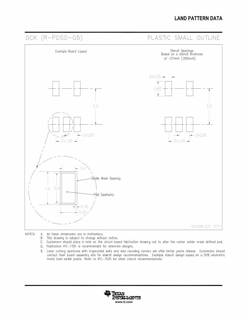
Figure 31. SOT-23 Board Layout Example
20
LMV7239-Q1JAJSF93 –APRIL 2018 www.tij.co.jp
Copyright © 2018, Texas Instruments Incorporated
11 デデババイイススおおよよびびドドキキュュメメンントトののササポポーートト
11.1 デデババイイスス・・ササポポーートト
11.1.1 開開発発ササポポーートトTINA-TI SPICEベースのアナログ・シミュレーション・プログラム、http://www.ti.com/tool/tina-ti
DIPアダプタ評価モジュール、http://www.ti.com/tool/dip-adapter-evm
TIユニバーサル・オペアンプ評価モジュール、http://www.ti.com/tool/opampevm
11.2 ドドキキュュメメンントトののササポポーートト
11.2.1 関関連連資資料料『独立して動作する4つのコンパレータ』(SNOA654)
11.3 ドドキキュュメメンントトのの更更新新通通知知をを受受けけ取取るる方方法法ドキュメントの更新についての通知を受け取るには、ti.comのデバイス製品フォルダを開いてください。右上の隅にある「通知を受け取る」をクリックして登録すると、変更されたすべての製品情報に関するダイジェストを毎週受け取れます。変更の詳細については、修正されたドキュメントに含まれている改訂履歴をご覧ください。
11.4 ココミミュュニニテティィ・・リリソソーーススThe following links connect to TI community resources. Linked contents are provided "AS IS" by the respectivecontributors. They do not constitute TI specifications and do not necessarily reflect TI's views; see TI's Terms ofUse.
TI E2E™オオンンラライインン・・ココミミュュニニテティィ TIののE2E((Engineer-to-Engineer))ココミミュュニニテティィ。。エンジニア間の共同作業を促進するために開設されたものです。e2e.ti.comでは、他のエンジニアに質問し、知識を共有し、アイディアを検討して、問題解決に役立てることができます。
設設計計ササポポーートト TIのの設設計計ササポポーートト役に立つE2Eフォーラムや、設計サポート・ツールをすばやく見つけることができます。技術サポート用の連絡先情報も参照できます。
11.5 商商標標E2E is a trademark of Texas Instruments.All other trademarks are the property of their respective owners.
11.6 静静電電気気放放電電にに関関すするる注注意意事事項項すべての集積回路は、適切なESD保護方法を用いて、取扱いと保存を行うようにして下さい。
静電気放電はわずかな性能の低下から完全なデバイスの故障に至るまで、様々な損傷を与えます。高精度の集積回路は、損傷に対して敏感であり、極めてわずかなパラメータの変化により、デバイスに規定された仕様に適合しなくなる場合があります。
11.7 GlossarySLYZ022 — TI Glossary.
This glossary lists and explains terms, acronyms, and definitions.
12 メメカカニニカカルル、、パパッッケケーージジ、、おおよよびび注注文文情情報報以降のページには、メカニカル、パッケージ、および注文に関する情報が記載されています。この情報は、そのデバイスについて利用可能な最新のデータです。このデータは予告なく変更されることがあり、ドキュメントが改訂される場合もあります。本データシートのブラウザ版を使用されている場合は、画面左側の説明をご覧ください。
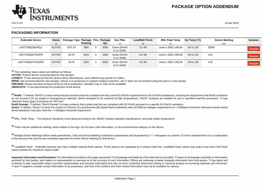
PACKAGE OPTION ADDENDUM
www.ti.com 18-Apr-2018
Addendum-Page 1
PACKAGING INFORMATION
Orderable Device Status(1)
Package Type PackageDrawing
Pins PackageQty
Eco Plan(2)
Lead/Ball Finish(6)
MSL Peak Temp(3)
Op Temp (°C) Device Marking(4/5)
Samples
LMV7239QDBVRQ1 ACTIVE SOT-23 DBV 5 3000 Green (RoHS& no Sb/Br)
CU SN Level-1-260C-UNLIM -40 to 125 ZBMX
LMV7239QM7/NOPB ACTIVE SC70 DCK 5 1000 Green (RoHS& no Sb/Br)
CU SN Level-1-260C-UNLIM -40 to 125 C42
LMV7239QM7X/NOPB ACTIVE SC70 DCK 5 3000 Green (RoHS& no Sb/Br)
CU SN Level-1-260C-UNLIM -40 to 125 C42
(1) The marketing status values are defined as follows:ACTIVE: Product device recommended for new designs.LIFEBUY: TI has announced that the device will be discontinued, and a lifetime-buy period is in effect.NRND: Not recommended for new designs. Device is in production to support existing customers, but TI does not recommend using this part in a new design.PREVIEW: Device has been announced but is not in production. Samples may or may not be available.OBSOLETE: TI has discontinued the production of the device.
(2) RoHS: TI defines "RoHS" to mean semiconductor products that are compliant with the current EU RoHS requirements for all 10 RoHS substances, including the requirement that RoHS substancedo not exceed 0.1% by weight in homogeneous materials. Where designed to be soldered at high temperatures, "RoHS" products are suitable for use in specified lead-free processes. TI mayreference these types of products as "Pb-Free".RoHS Exempt: TI defines "RoHS Exempt" to mean products that contain lead but are compliant with EU RoHS pursuant to a specific EU RoHS exemption.Green: TI defines "Green" to mean the content of Chlorine (Cl) and Bromine (Br) based flame retardants meet JS709B low halogen requirements of <=1000ppm threshold. Antimony trioxide basedflame retardants must also meet the <=1000ppm threshold requirement.
(3) MSL, Peak Temp. - The Moisture Sensitivity Level rating according to the JEDEC industry standard classifications, and peak solder temperature.
(4) There may be additional marking, which relates to the logo, the lot trace code information, or the environmental category on the device.
(5) Multiple Device Markings will be inside parentheses. Only one Device Marking contained in parentheses and separated by a "~" will appear on a device. If a line is indented then it is a continuationof the previous line and the two combined represent the entire Device Marking for that device.
(6) Lead/Ball Finish - Orderable Devices may have multiple material finish options. Finish options are separated by a vertical ruled line. Lead/Ball Finish values may wrap to two lines if the finishvalue exceeds the maximum column width.
Important Information and Disclaimer:The information provided on this page represents TI's knowledge and belief as of the date that it is provided. TI bases its knowledge and belief on informationprovided by third parties, and makes no representation or warranty as to the accuracy of such information. Efforts are underway to better integrate information from third parties. TI has taken andcontinues to take reasonable steps to provide representative and accurate information but may not have conducted destructive testing or chemical analysis on incoming materials and chemicals.TI and TI suppliers consider certain information to be proprietary, and thus CAS numbers and other limited information may not be available for release.
PACKAGE OPTION ADDENDUM
www.ti.com 18-Apr-2018
Addendum-Page 2
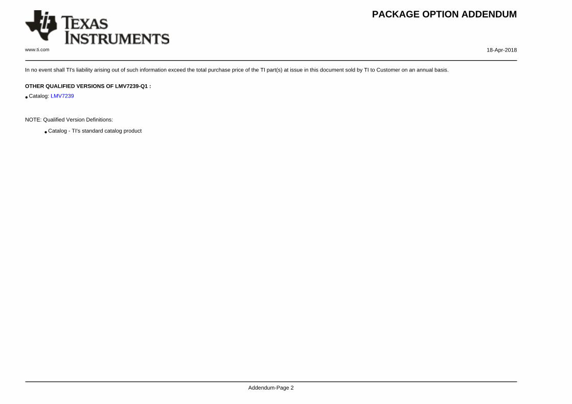
In no event shall TI's liability arising out of such information exceed the total purchase price of the TI part(s) at issue in this document sold by TI to Customer on an annual basis.
OTHER QUALIFIED VERSIONS OF LMV7239-Q1 :
• Catalog: LMV7239
NOTE: Qualified Version Definitions:
• Catalog - TI's standard catalog product
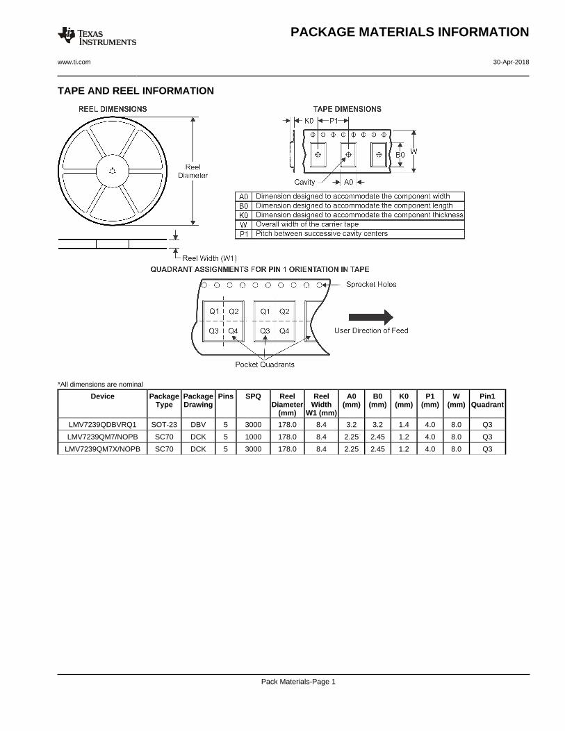
TAPE AND REEL INFORMATION
*All dimensions are nominal
Device PackageType
PackageDrawing
Pins SPQ ReelDiameter
(mm)
ReelWidth
W1 (mm)
A0(mm)
B0(mm)
K0(mm)
P1(mm)
W(mm)
Pin1Quadrant
LMV7239QDBVRQ1 SOT-23 DBV 5 3000 178.0 8.4 3.2 3.2 1.4 4.0 8.0 Q3
LMV7239QM7/NOPB SC70 DCK 5 1000 178.0 8.4 2.25 2.45 1.2 4.0 8.0 Q3
LMV7239QM7X/NOPB SC70 DCK 5 3000 178.0 8.4 2.25 2.45 1.2 4.0 8.0 Q3
PACKAGE MATERIALS INFORMATION
www.ti.com 30-Apr-2018
Pack Materials-Page 1
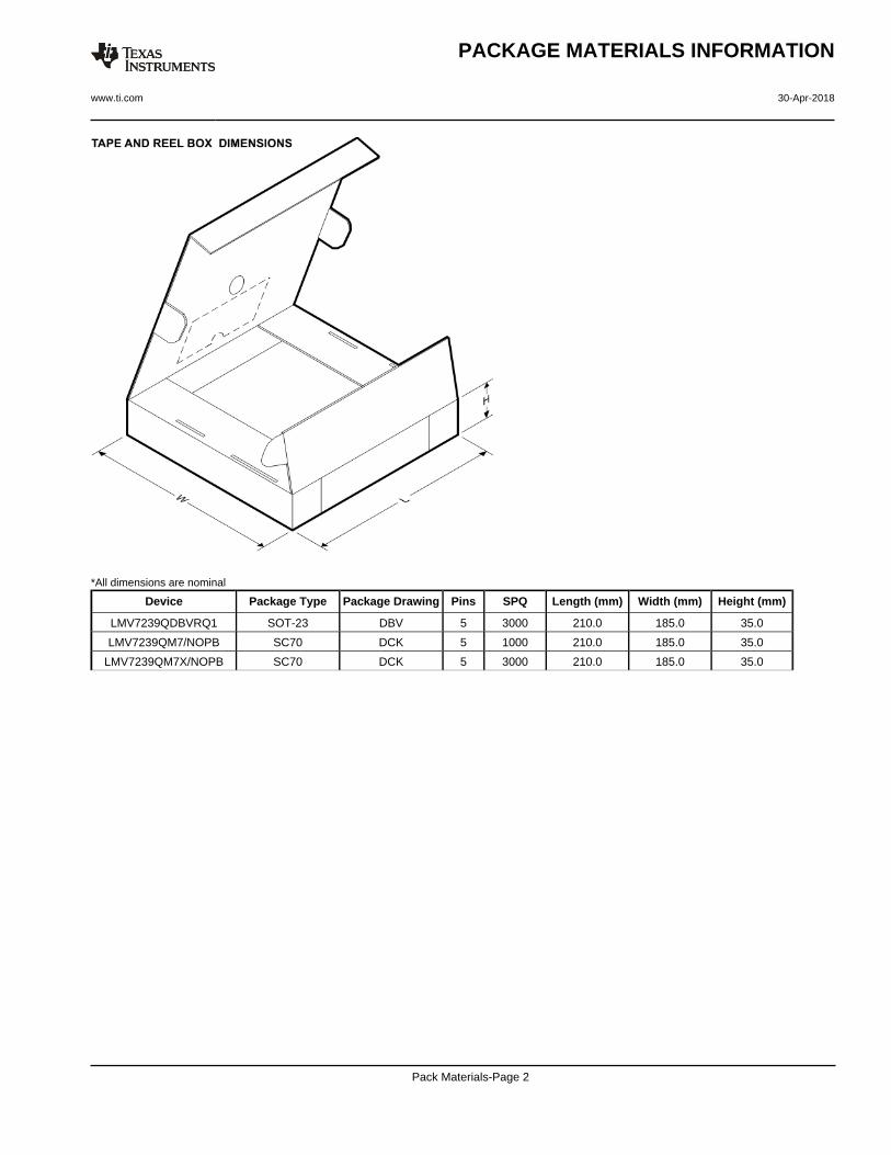
*All dimensions are nominal
Device Package Type Package Drawing Pins SPQ Length (mm) Width (mm) Height (mm)
LMV7239QDBVRQ1 SOT-23 DBV 5 3000 210.0 185.0 35.0
LMV7239QM7/NOPB SC70 DCK 5 1000 210.0 185.0 35.0
LMV7239QM7X/NOPB SC70 DCK 5 3000 210.0 185.0 35.0
PACKAGE MATERIALS INFORMATION
www.ti.com 30-Apr-2018
Pack Materials-Page 2
www.ti.com
PACKAGE OUTLINE
C
TYP0.220.08
0.25
3.02.6
2X 0.95
1.9
1.45 MAX
TYP0.150.00
5X 0.50.3
TYP0.60.3
TYP80
1.9
A
3.052.75
B1.751.45
(1.1)
SOT-23 - 1.45 mm max heightDBV0005ASMALL OUTLINE TRANSISTOR
4214839/C 04/2017
NOTES: 1. All linear dimensions are in millimeters. Any dimensions in parenthesis are for reference only. Dimensioning and tolerancing per ASME Y14.5M.2. This drawing is subject to change without notice.3. Refernce JEDEC MO-178.
0.2 C A B
1
34
5
2
INDEX AREAPIN 1
GAGE PLANE
SEATING PLANE
0.1 C
SCALE 4.000
www.ti.com
EXAMPLE BOARD LAYOUT
0.07 MAXARROUND
0.07 MINARROUND
5X (1.1)
5X (0.6)
(2.6)
(1.9)
2X (0.95)
(R0.05) TYP
4214839/C 04/2017
SOT-23 - 1.45 mm max heightDBV0005ASMALL OUTLINE TRANSISTOR
NOTES: (continued) 4. Publication IPC-7351 may have alternate designs. 5. Solder mask tolerances between and around signal pads can vary based on board fabrication site.
SYMM
LAND PATTERN EXAMPLEEXPOSED METAL SHOWN
SCALE:15X
PKG
1
3 4
5
2
SOLDER MASKOPENINGMETAL UNDER
SOLDER MASK
SOLDER MASKDEFINED
EXPOSED METAL
METALSOLDER MASKOPENING
NON SOLDER MASKDEFINED
(PREFERRED)
SOLDER MASK DETAILS
EXPOSED METAL
www.ti.com
EXAMPLE STENCIL DESIGN
(2.6)
(1.9)
2X(0.95)
5X (1.1)
5X (0.6)
(R0.05) TYP
SOT-23 - 1.45 mm max heightDBV0005ASMALL OUTLINE TRANSISTOR
4214839/C 04/2017
NOTES: (continued) 6. Laser cutting apertures with trapezoidal walls and rounded corners may offer better paste release. IPC-7525 may have alternate design recommendations. 7. Board assembly site may have different recommendations for stencil design.
SOLDER PASTE EXAMPLEBASED ON 0.125 mm THICK STENCIL
SCALE:15X
SYMM
PKG
1
3 4
5
2
重重要要ななおお知知ららせせ
Texas Instruments Incorporated (TI)は、JESD46の最新版に従って自社の半導体製品およびサービスに訂正、拡張、改良、および、その他の変更を加える権利と、JESD48の最新版に従って任意の製品またはサービスを打ち切る権利を留保します。購入者は発注を行う前に、最新の関連情報を取得し、それらの情報が最新かつ完全なものであることを確認する義務があります。
TIの半導体製品に関する公開済みの販売条項(http://www.tij.co.jp/general/jp/docs/gencontent.tsp?contentId=27309)は、TIが認定し、市場へリリースしたパッケージ集積回路製品の販売に適用されます。他の種類のTI製品およびサービスの使用または販売については、追加条項が適用される場合があります。
TIデータシートに記載されているTI情報の重要な部分の複製は、その情報に一切の変更を加えることなく、かつ、その情報に関連するすべての保証、条件、制限、通知が付属する場合のみ許可されます。このような複製文書について、TIは一切の責任または義務を負いません。第三者の情報については、さらに別の制限が課される可能性があります。TI製品またはサービスの再販において、その製品またはサービスについてTIが規定したパラメータと異なるか、それを超える記述を付すことは不公正かつ欺瞞的な商慣習であり、そのような場合、関連するTI製品またはサービスに関する明示的および黙示的な保証のすべてが無効となります。このような記述について、TIは一切責任または義務を負いません。
購入者、およびTI製品を組み込んだシステムを開発する他者(以下、「設計者」と総称します)は、自らのアプリケーションの設計において、独自の分析、評価、判断を行う責任は設計者自身にあること、および、設計者のアプリケーション(および、設計者のアプリケーションに使用されるすべてのTI製品)の安全性、および該当するすべての規制、法、その他適用される要件の遵守を保証するすべての責任は設計者のみが負うことを理解し、同意するものとします。設計者は、自身のアプリケーションに関して、(1) 危険な不具合から生じる結果を予期し、(2) 不具合およびその結果を監視し、また、(3) 害を及ぼす不具合の可能性を低減するため、保全策を策定および実施し、かつ、適切な是正措置を講じるうえで必要な専門的知識を持つことを表明するものとします。設計者は、TI製品を含むいずれかのアプリケーションを使用または配布する前に、そのアプリケーション、および、アプリケーションで使用されるTI製品の機能を完全にテストすることに同意するものとします。
TIの技術、アプリケーションまたはその他の設計に関する助言、品質特性、信頼性のデータ、もしくは、他のサービスまたは情報は、TI製品を組み込んだアプリケーションを開発する設計者に役立つことを目的として提供するものです。これにはリファレンス設計や、評価モジュールに関係する資料が含まれますが、これらに限られません(以下、これらを総称して「TIリソース」とします)。いかなる方法であっても、TIリソースのいずれかをダウンロード、アクセス、または使用した場合、設計者(個人、または会社を代表している場合には設計者の会社)は、TIリソースをここに記載された目的にのみ使用し、この注意事項の条項に従うことに同意したものとします。
TIによるTIリソースの提供は、TI製品に対する該当の発行済み保証事項または免責事項を、拡張、またはどのような形でも変更するものではなく、これらのTIリソースを提供することによって、TIにはいかなる追加義務または責任も発生しません。TIは、自社のTIリソースに訂正、拡張、改良、および、その他の変更を加える権利を留保します。TIは、特定のTIリソース用に発行されたドキュメントで明示的に記載されている以外のテストを実行していません。
設計者は、個別のTIリソースを、そのTIリソースに記載されているTI製品を搭載したアプリケーションの開発に関連する目的でのみ、使用、複製、および改変することが認められています。明示または黙示を問わず、禁反言の法理その他どのような理由でも、他のTIの知的所有権に対するその他のライセンスは与えられず、ITまたはいかなる第三者のテクノロジまたは知的所有権についても、いかなるライセンスも与えるものではありません。これには、TI製品またはサービスが使用される組み合わせ、機械、またはプロセスに関連する特許権、著作権、回路配置利用権、その他の知的所有権が含まれますが、これらに限られません。第三者の製品やサービスに関する、またはそれらを参照する情報は、そのような製品またはサービスを利用するライセンスを構成するものではなく、それらに対する保証または推奨を意味するものでもありません。TIリソースを使用するため、第三者の特許または他の知的所有権に基づく第三者からのライセンス、もしくは、TIの特許または他の知的所有権に基づくTIからのライセンスが必要な場合があります。
TIのリソースは、それに含まれるあらゆる欠陥も含めて、「現状のまま」提供されます。TIは、TIリソースまたはその使用に関して、明示か黙示かにかかわらず、他のいかなる保証または表明も行いません。これには、正確性または完全性、権原、続発性の障害に関する保証、ならびに、商品性、特定目的への適合性、および、第三者の知的所有権の非侵害に対する黙示の保証が含まれますが、これらに限られません。TIは、設計者への弁護または補償を行う義務はなく、行わないものとします。これには、任意の製品の組み合わせに関する、または、それらに基づく侵害の請求も含まれますが、これらに限られず、また、その事実についてTIリソースまたはその他の場所に記載されているか否かを問わないものとします。いかなる場合も、TIリソースまたはその使用に関連して、またはそれらにより発生した、実際、直接的、特別、付随的、間接的、懲罰的、偶発的、または、結果的な損害について、そのような損害の可能性についてTIが知らされていたか否かにかかわらず、TIは責任を負わないものとします。
TIが特定の業界標準(例えば、ISO/TS 16949およびISO 26262を含む。)の要求に適合していることを明示的に指定した個々の本製品でない限り、TIは、業界標準の要求事項を満たしていなかったことについて、いかなる責任も負いません 。
TIが製品について、機能的安全性の促進、または業界の機能的安全性基準の遵守を特に推進している場合、そのような製品は、お客様が該当の機能的安全性基準および要件を満たすアプリケーションを自ら設計および製作するために役立てることを意図したものです。アプリケーションにこれらの製品を使用することのみで、アプリケーションの安全性が確立されるものではありません。設計者は、自らのアプリケーションについて、該当する安全性関連の要件および基準の遵守を保証する必要があります。設計者は、安全でないことが致命的となる医療機器にTI製品を使用してはいけません。但し、両当事者の権限のある役員間で、かかる使用について具体的に規定した特別な契約が締結された場合はその限りではありません。安全でないことが致命的となる医療機器とは、かかる機器の不具合が重大な身体的障害又は死亡を引き起こすものを指し、生命維持装置、ペースメーカー、除細動器、心臓マッサージ機、神経刺激装置および移植医療機器を含みます。かかる機器には米国の食品医薬品局(FDA)がクラスIIIに指定するもの、また、米国外で同等に分類されているものを含みますがこれらに限られません。
TIは、特定の本製品が特別な品質(Q100、軍需対応グレード品、機能強化製品を例とする。)を満たしていることを明示的に指定することがあります。設計者は、自らのアプリケーションに適した品質が確保された本製品を選択するために必要な専門的知識を持ち、かつ、本製品の選択は設計者の責任で行うことに同意するものとします。設計者は、かかる選択に関連して、法規制で要求される事項を遵守する責任を単独で負うものとします。
設計者は、自らがこのお知らせの条項および条件に従わなかったために発生した、いかなる損害、コスト、損失、責任からも、TIおよびその代表者を完全に免責するものとします。IMPORTANT NOTICE
Copyright © 2018, Texas Instruments Incorporated日本語版 日本テキサス・インスツルメンツ株式会社


![Czy naprawdę liczy się tylko - Termedia · PDF fileRosuvastatin Slide Kit May 2004 [17] Rosuvastatin versus Comparators: LDL-C Efficacy at Low Dose The STELLAR Study Change in LDL-C](https://img.pdfslide.tips/doc/110x75/5ab75f067f8b9a28468b79c9/czy-naprawde-liczy-sie-tylko-termedia-slide-kit-may-2004-17-rosuvastatin-versus.jpg)