Embed Size (px)
Citation preview
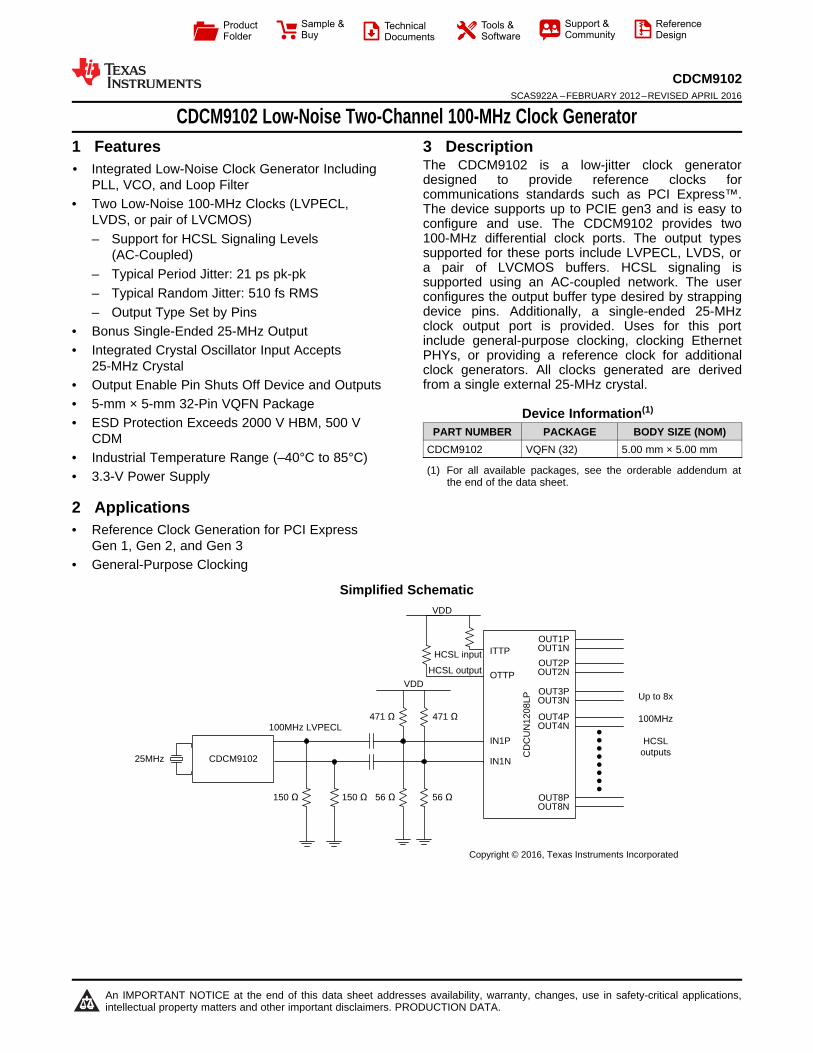
CDCM9102
100MHz LVPECL
CD
CU
N12
08LP
VDD
25MHz
HCSL input
HCSL output
VDD
150 �� 56 ��
471 �� 471 ��
Up to 8x
100MHz
HCSL outputs
150 �� 56 ��
ITTP
OTTP
IN1P
IN1N
OUT1POUT1N
OUT2POUT2N
OUT3POUT3N
OUT4POUT4N
OUT8POUT8N
Copyright © 2016, Texas Instruments Incorporated
Product
Folder
Sample &Buy
Technical
Documents
Tools &
Software
Support &Community
ReferenceDesign
An IMPORTANT NOTICE at the end of this data sheet addresses availability, warranty, changes, use in safety-critical applications,intellectual property matters and other important disclaimers. PRODUCTION DATA.
CDCM9102SCAS922A –FEBRUARY 2012–REVISED APRIL 2016
CDCM9102 Low-Noise Two-Channel 100-MHz Clock Generator
1
1 Features1• Integrated Low-Noise Clock Generator Including
PLL, VCO, and Loop Filter• Two Low-Noise 100-MHz Clocks (LVPECL,
LVDS, or pair of LVCMOS)– Support for HCSL Signaling Levels
(AC-Coupled)– Typical Period Jitter: 21 ps pk-pk– Typical Random Jitter: 510 fs RMS– Output Type Set by Pins
• Bonus Single-Ended 25-MHz Output• Integrated Crystal Oscillator Input Accepts
25-MHz Crystal• Output Enable Pin Shuts Off Device and Outputs• 5-mm × 5-mm 32-Pin VQFN Package• ESD Protection Exceeds 2000 V HBM, 500 V
CDM• Industrial Temperature Range (–40°C to 85°C)• 3.3-V Power Supply
2 Applications• Reference Clock Generation for PCI Express
Gen 1, Gen 2, and Gen 3• General-Purpose Clocking
3 DescriptionThe CDCM9102 is a low-jitter clock generatordesigned to provide reference clocks forcommunications standards such as PCI Express™.The device supports up to PCIE gen3 and is easy toconfigure and use. The CDCM9102 provides two100-MHz differential clock ports. The output typessupported for these ports include LVPECL, LVDS, ora pair of LVCMOS buffers. HCSL signaling issupported using an AC-coupled network. The userconfigures the output buffer type desired by strappingdevice pins. Additionally, a single-ended 25-MHzclock output port is provided. Uses for this portinclude general-purpose clocking, clocking EthernetPHYs, or providing a reference clock for additionalclock generators. All clocks generated are derivedfrom a single external 25-MHz crystal.
Device Information(1)
PART NUMBER PACKAGE BODY SIZE (NOM)CDCM9102 VQFN (32) 5.00 mm × 5.00 mm
(1) For all available packages, see the orderable addendum atthe end of the data sheet.
Simplified Schematic
2
CDCM9102SCAS922A –FEBRUARY 2012–REVISED APRIL 2016 www.ti.com
Product Folder Links: CDCM9102
Submit Documentation Feedback Copyright © 2012–2016, Texas Instruments Incorporated
Table of Contents1 Features .................................................................. 12 Applications ........................................................... 13 Description ............................................................. 14 Revision History..................................................... 25 Device Comparison Table ..................................... 36 Pin Configuration and Functions ......................... 37 Specifications......................................................... 5
7.1 Absolute Maximum Ratings ...................................... 57.2 ESD Ratings.............................................................. 57.3 Recommended Operating Conditions....................... 57.4 Thermal Information .................................................. 57.5 Electrical Characteristics........................................... 67.6 Timing Requirements ................................................ 77.7 Typical Characteristics .............................................. 7
8 Parameter Measurement Information .................. 88.1 Test Configurations ................................................... 8
9 Detailed Description ............................................ 109.1 Overview ................................................................. 109.2 Functional Block Diagrams ..................................... 10
9.3 Feature Description................................................. 109.4 Device Functional Modes ....................................... 109.5 Programming........................................................... 12
10 Application and Implementation........................ 1310.1 Application Information.......................................... 1310.2 Typical Application ................................................ 16
11 Power Supply Recommendations ..................... 1911.1 Thermal Management ........................................... 1911.2 Power Supply Filtering .......................................... 19
12 Layout................................................................... 2012.1 Layout Guidelines ................................................. 2012.2 Layout Example .................................................... 20
13 Device and Documentation Support ................. 2113.1 Community Resources.......................................... 2113.2 Trademarks ........................................................... 2113.3 Electrostatic Discharge Caution............................ 2113.4 Glossary ................................................................ 21
14 Mechanical, Packaging, and OrderableInformation ........................................................... 21
4 Revision HistoryNOTE: Page numbers for previous revisions may differ from page numbers in the current version.
Changes from Original (February 2012) to Revision A Page
• Added ESD Ratings table, Feature Description section, Device Functional Modes, Application and Implementationsection, Power Supply Recommendations section, Layout section, Device and Documentation Support section, andMechanical, Packaging, and Orderable Information section .................................................................................................. 1
• Added text to Description: The device supports up to PCIE gen3 and is .............................................................................. 1• Changed part number to 1134 25M0000000 ....................................................................................................................... 11• Changed part number to FP2500002................................................................................................................................... 11• Added text and Figure 16 to PCI Express Applications ....................................................................................................... 15
GND
24
NC
1V
DD
2
25NC 16 VDD4
23
OS
CO
UT
2O
UT
1N
26NC 15 NC
22
GN
D3
OU
T1
P
27NC 14 GND
21
XIN
4V
DD
1
28NC 13 NC
20
VD
D6
5O
UT
0N
29NC 12 RESET
19
RE
GC
AP
16
OU
T0
P
30NC 11 OS0
18
VD
D5
7O
E
31NC 10 OS1
17
RE
GC
AP
28
NC
32NC 9 VDD3
3
CDCM9102www.ti.com SCAS922A –FEBRUARY 2012–REVISED APRIL 2016
Product Folder Links: CDCM9102
Submit Documentation FeedbackCopyright © 2012–2016, Texas Instruments Incorporated
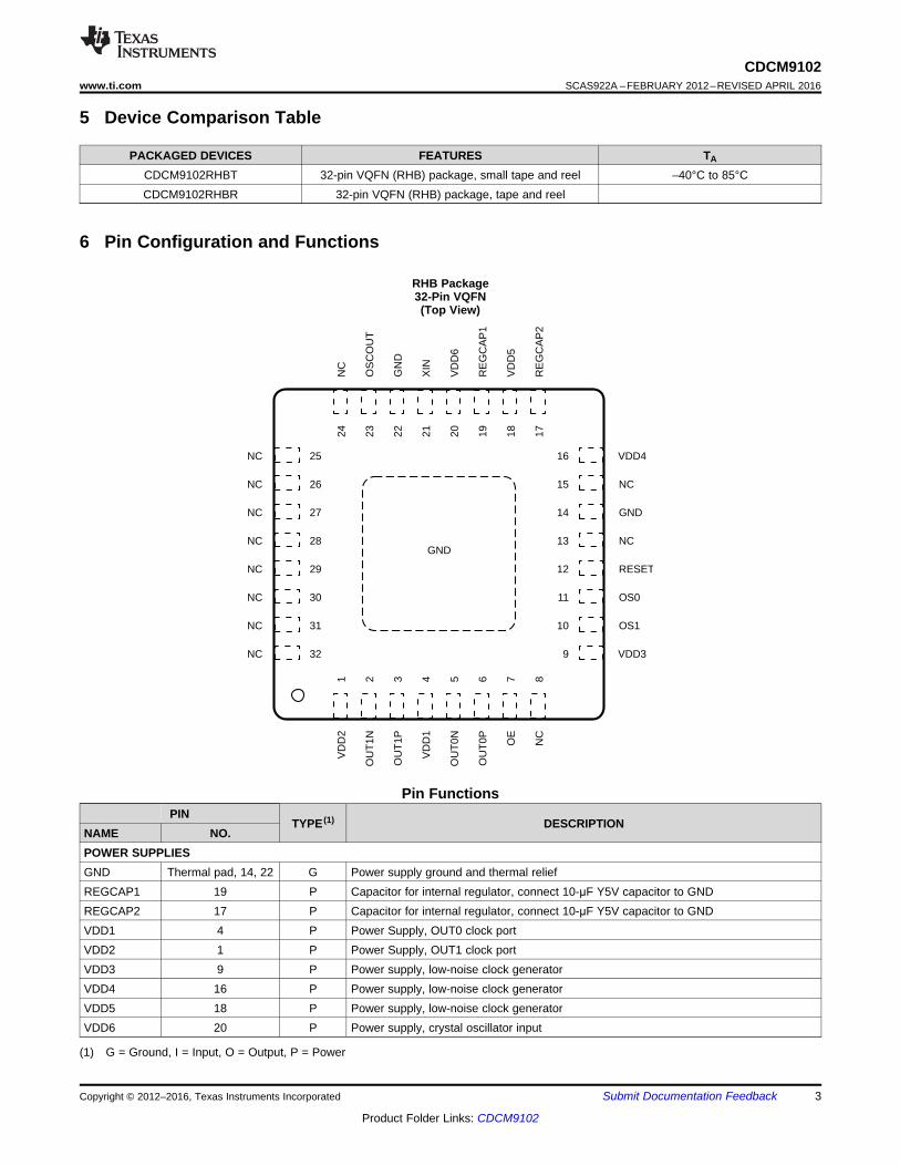
5 Device Comparison Table
PACKAGED DEVICES FEATURES TA
CDCM9102RHBT 32-pin VQFN (RHB) package, small tape and reel –40°C to 85°CCDCM9102RHBR 32-pin VQFN (RHB) package, tape and reel
(1) G = Ground, I = Input, O = Output, P = Power
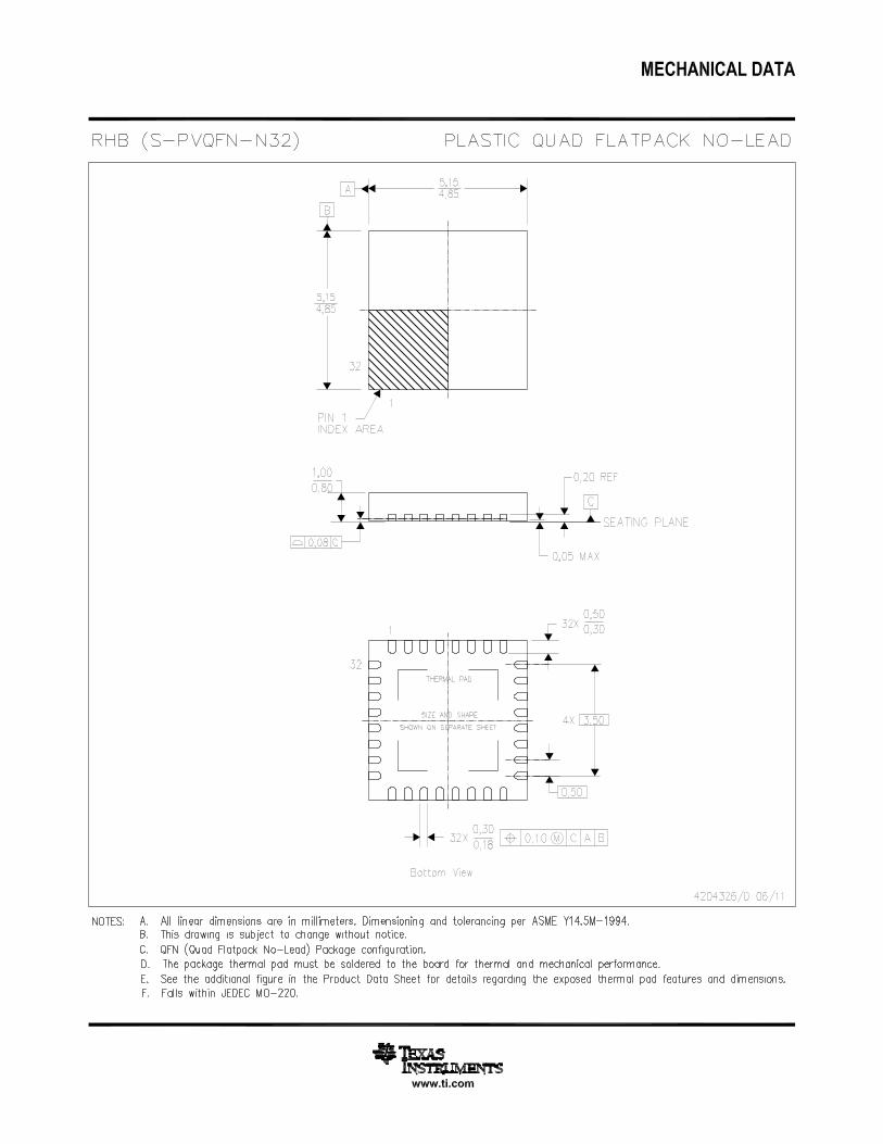
6 Pin Configuration and Functions
RHB Package32-Pin VQFN(Top View)
Pin FunctionsPIN
TYPE (1) DESCRIPTIONNAME NO.POWER SUPPLIESGND Thermal pad, 14, 22 G Power supply ground and thermal reliefREGCAP1 19 P Capacitor for internal regulator, connect 10-μF Y5V capacitor to GNDREGCAP2 17 P Capacitor for internal regulator, connect 10-μF Y5V capacitor to GNDVDD1 4 P Power Supply, OUT0 clock portVDD2 1 P Power Supply, OUT1 clock portVDD3 9 P Power supply, low-noise clock generatorVDD4 16 P Power supply, low-noise clock generatorVDD5 18 P Power supply, low-noise clock generatorVDD6 20 P Power supply, crystal oscillator input
4
CDCM9102SCAS922A –FEBRUARY 2012–REVISED APRIL 2016 www.ti.com
Product Folder Links: CDCM9102
Submit Documentation Feedback Copyright © 2012–2016, Texas Instruments Incorporated
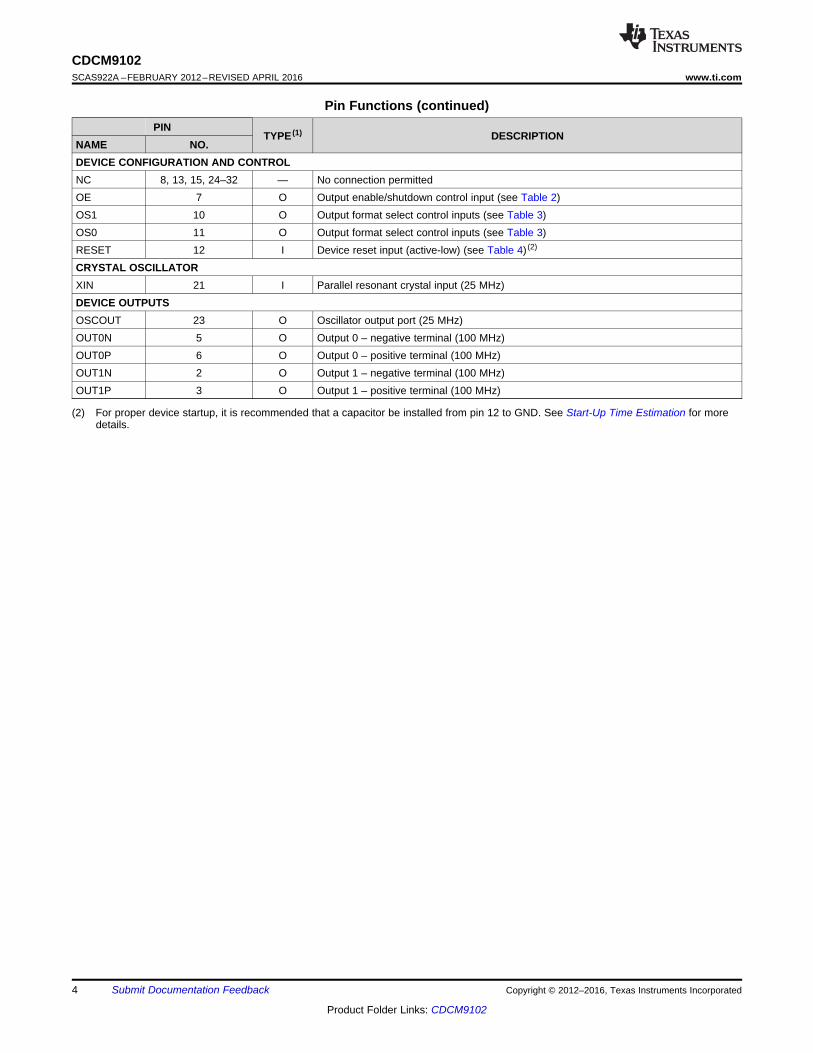
Pin Functions (continued)PIN
TYPE (1) DESCRIPTIONNAME NO.
(2) For proper device startup, it is recommended that a capacitor be installed from pin 12 to GND. See Start-Up Time Estimation for moredetails.
DEVICE CONFIGURATION AND CONTROLNC 8, 13, 15, 24–32 — No connection permittedOE 7 O Output enable/shutdown control input (see Table 2)OS1 10 O Output format select control inputs (see Table 3)OS0 11 O Output format select control inputs (see Table 3)RESET 12 I Device reset input (active-low) (see Table 4) (2)
CRYSTAL OSCILLATORXIN 21 I Parallel resonant crystal input (25 MHz)DEVICE OUTPUTSOSCOUT 23 O Oscillator output port (25 MHz)OUT0N 5 O Output 0 – negative terminal (100 MHz)OUT0P 6 O Output 0 – positive terminal (100 MHz)OUT1N 2 O Output 1 – negative terminal (100 MHz)OUT1P 3 O Output 1 – positive terminal (100 MHz)
5
CDCM9102www.ti.com SCAS922A –FEBRUARY 2012–REVISED APRIL 2016
Product Folder Links: CDCM9102
Submit Documentation FeedbackCopyright © 2012–2016, Texas Instruments Incorporated
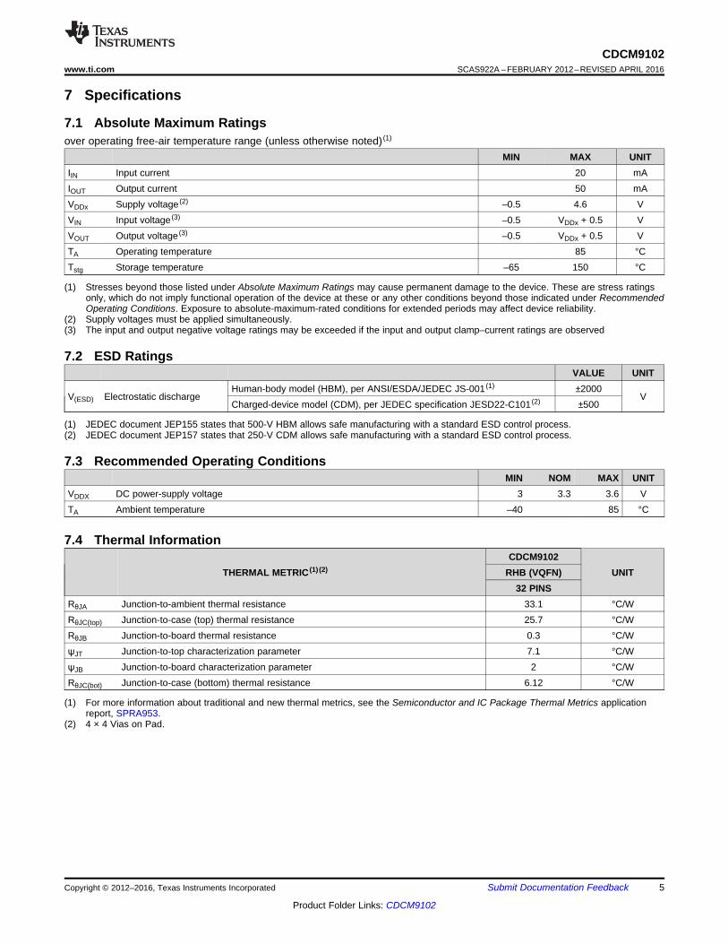
(1) Stresses beyond those listed under Absolute Maximum Ratings may cause permanent damage to the device. These are stress ratingsonly, which do not imply functional operation of the device at these or any other conditions beyond those indicated under RecommendedOperating Conditions. Exposure to absolute-maximum-rated conditions for extended periods may affect device reliability.
(2) Supply voltages must be applied simultaneously.(3) The input and output negative voltage ratings may be exceeded if the input and output clamp–current ratings are observed
7 Specifications
7.1 Absolute Maximum Ratingsover operating free-air temperature range (unless otherwise noted) (1)
MIN MAX UNITIIN Input current 20 mAIOUT Output current 50 mAVDDx Supply voltage (2) –0.5 4.6 VVIN Input voltage (3) –0.5 VDDx + 0.5 VVOUT Output voltage (3) –0.5 VDDx + 0.5 VTA Operating temperature 85 °CTstg Storage temperature –65 150 °C
(1) JEDEC document JEP155 states that 500-V HBM allows safe manufacturing with a standard ESD control process.(2) JEDEC document JEP157 states that 250-V CDM allows safe manufacturing with a standard ESD control process.
7.2 ESD RatingsVALUE UNIT
V(ESD) Electrostatic dischargeHuman-body model (HBM), per ANSI/ESDA/JEDEC JS-001 (1) ±2000
VCharged-device model (CDM), per JEDEC specification JESD22-C101 (2) ±500
7.3 Recommended Operating ConditionsMIN NOM MAX UNIT
VDDX DC power-supply voltage 3 3.3 3.6 VTA Ambient temperature –40 85 °C
(1) For more information about traditional and new thermal metrics, see the Semiconductor and IC Package Thermal Metrics applicationreport, SPRA953.
(2) 4 × 4 Vias on Pad.
7.4 Thermal Information
THERMAL METRIC (1) (2)CDCM9102
UNITRHB (VQFN)32 PINS
RθJA Junction-to-ambient thermal resistance 33.1 °C/WRθJC(top) Junction-to-case (top) thermal resistance 25.7 °C/WRθJB Junction-to-board thermal resistance 0.3 °C/WψJT Junction-to-top characterization parameter 7.1 °C/WψJB Junction-to-board characterization parameter 2 °C/WRθJC(bot) Junction-to-case (bottom) thermal resistance 6.12 °C/W
6
CDCM9102SCAS922A –FEBRUARY 2012–REVISED APRIL 2016 www.ti.com
Product Folder Links: CDCM9102
Submit Documentation Feedback Copyright © 2012–2016, Texas Instruments Incorporated
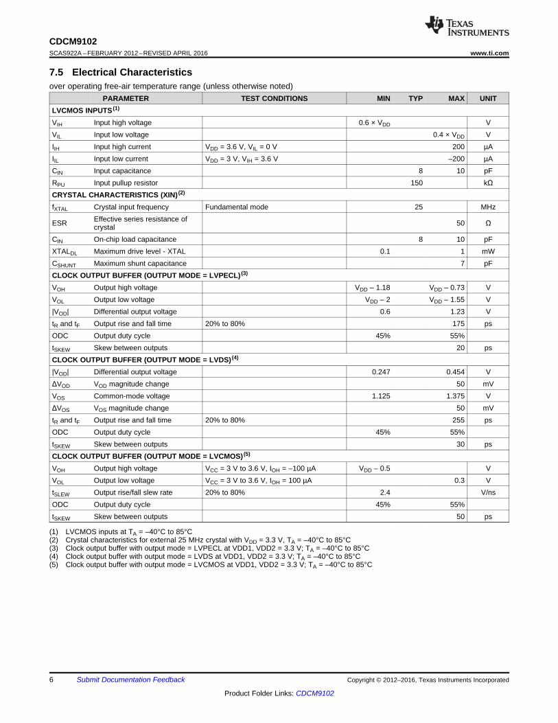
(1) LVCMOS inputs at TA = –40°C to 85°C(2) Crystal characteristics for external 25 MHz crystal with VDD = 3.3 V, TA = –40°C to 85°C(3) Clock output buffer with output mode = LVPECL at VDD1, VDD2 = 3.3 V; TA = –40°C to 85°C(4) Clock output buffer with output mode = LVDS at VDD1, VDD2 = 3.3 V; TA = –40°C to 85°C(5) Clock output buffer with output mode = LVCMOS at VDD1, VDD2 = 3.3 V; TA = –40°C to 85°C
7.5 Electrical Characteristicsover operating free-air temperature range (unless otherwise noted)
PARAMETER TEST CONDITIONS MIN TYP MAX UNITLVCMOS INPUTS (1)
VIH Input high voltage 0.6 × VDD VVIL Input low voltage 0.4 × VDD VIIH Input high current VDD = 3.6 V, VIL = 0 V 200 µAIIL Input low current VDD = 3 V, VIH = 3.6 V –200 µACIN Input capacitance 8 10 pFRPU Input pullup resistor 150 kΩCRYSTAL CHARACTERISTICS (XIN) (2)
fXTAL Crystal input frequency Fundamental mode 25 MHz
ESR Effective series resistance ofcrystal 50 Ω
CIN On-chip load capacitance 8 10 pFXTALDL Maximum drive level - XTAL 0.1 1 mWCSHUNT Maximum shunt capacitance 7 pFCLOCK OUTPUT BUFFER (OUTPUT MODE = LVPECL) (3)
VOH Output high voltage VDD – 1.18 VDD – 0.73 VVOL Output low voltage VDD – 2 VDD – 1.55 V|VOD| Differential output voltage 0.6 1.23 VtR and tF Output rise and fall time 20% to 80% 175 psODC Output duty cycle 45% 55%tSKEW Skew between outputs 20 psCLOCK OUTPUT BUFFER (OUTPUT MODE = LVDS) (4)
|VOD| Differential output voltage 0.247 0.454 VΔVOD VOD magnitude change 50 mVVOS Common-mode voltage 1.125 1.375 VΔVOS VOS magnitude change 50 mVtR and tF Output rise and fall time 20% to 80% 255 psODC Output duty cycle 45% 55%tSKEW Skew between outputs 30 psCLOCK OUTPUT BUFFER (OUTPUT MODE = LVCMOS) (5)
VOH Output high voltage VCC = 3 V to 3.6 V, IOH = –100 µA VDD – 0.5 VVOL Output low voltage VCC = 3 V to 3.6 V, IOH = 100 µA 0.3 VtSLEW Output rise/fall slew rate 20% to 80% 2.4 V/nsODC Output duty cycle 45% 55%tSKEW Skew between outputs 50 ps
7
CDCM9102www.ti.com SCAS922A –FEBRUARY 2012–REVISED APRIL 2016
Product Folder Links: CDCM9102
Submit Documentation FeedbackCopyright © 2012–2016, Texas Instruments Incorporated
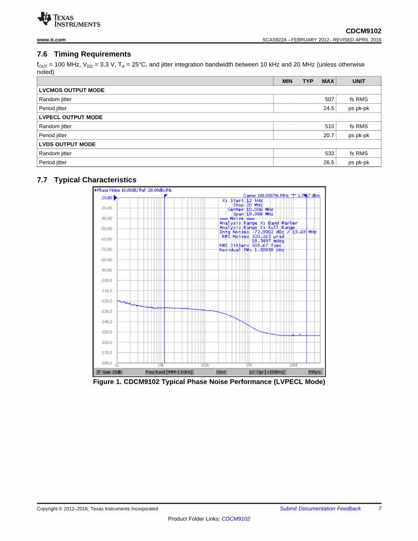
7.6 Timing RequirementsfOUT = 100 MHz, VDD = 3.3 V, TA = 25°C, and jitter integration bandwidth between 10 kHz and 20 MHz (unless otherwisenoted)
MIN TYP MAX UNITLVCMOS OUTPUT MODERandom jitter 507 fs RMSPeriod jitter 24.5 ps pk-pkLVPECL OUTPUT MODERandom jitter 510 fs RMSPeriod jitter 20.7 ps pk-pkLVDS OUTPUT MODERandom jitter 533 fs RMSPeriod jitter 26.5 ps pk-pk
7.7 Typical Characteristics
Figure 1. CDCM9102 Typical Phase Noise Performance (LVPECL Mode)
LVPECL
150 (2)W
Phase Noise Analyzer
RF
50 W
50 W
Oscilloscope
CH1 CH2
LVPECL
50 W
50 W
50 (2)W
V - 2 VDD
LVCMOS 50 W
Phase Noise Analyzer
RF
50 W
LVCMOS
5 pF
8
CDCM9102SCAS922A –FEBRUARY 2012–REVISED APRIL 2016 www.ti.com
Product Folder Links: CDCM9102
Submit Documentation Feedback Copyright © 2012–2016, Texas Instruments Incorporated
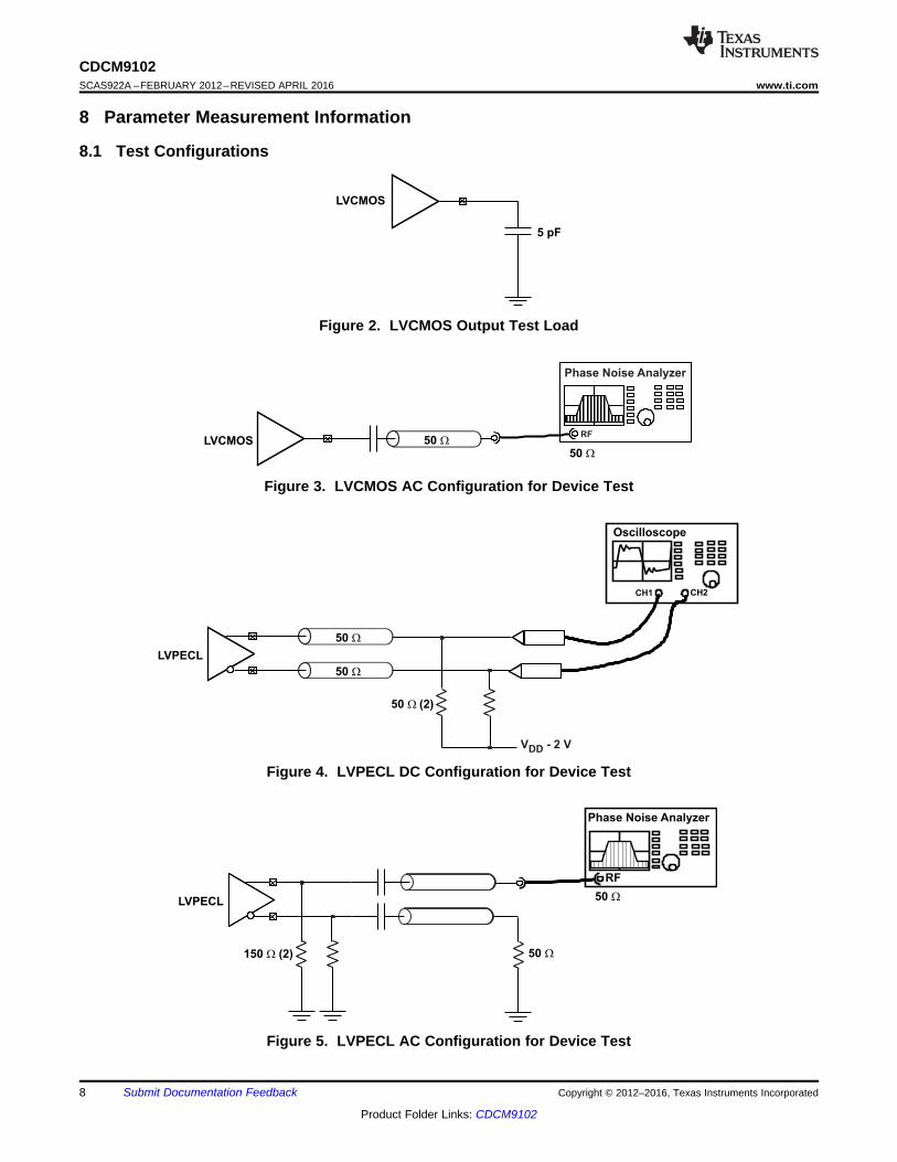
8 Parameter Measurement Information
8.1 Test Configurations
Figure 2. LVCMOS Output Test Load
Figure 3. LVCMOS AC Configuration for Device Test
Figure 4. LVPECL DC Configuration for Device Test
Figure 5. LVPECL AC Configuration for Device Test
LVDS
Phase Noise Analyzer
RF50 W
50 W
50 W
50 W
Oscilloscope
CH1 CH2
LVDS 100 W
50 W
50 W
9
CDCM9102www.ti.com SCAS922A –FEBRUARY 2012–REVISED APRIL 2016
Product Folder Links: CDCM9102
Submit Documentation FeedbackCopyright © 2012–2016, Texas Instruments Incorporated
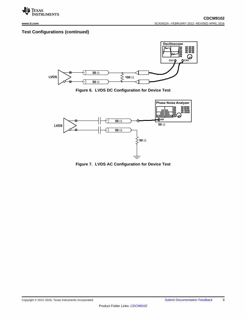
Test Configurations (continued)
Figure 6. LVDS DC Configuration for Device Test
Figure 7. LVDS AC Configuration for Device Test
XO
25 MHz CSTRAY CPARASITICCL CIN
XIN(Pin 21)
OS0OS1
CDCM9102
XO
LowNoiseClock
Generator
RESET
OE
OSCOUT
OUT1P
OUT1N
OUT0P
OUT0N
REGCAP1 REGCAP2
Copyright © 2016, Texas Instruments Incorporated
Vreg Vreg
10
CDCM9102SCAS922A –FEBRUARY 2012–REVISED APRIL 2016 www.ti.com
Product Folder Links: CDCM9102
Submit Documentation Feedback Copyright © 2012–2016, Texas Instruments Incorporated
9 Detailed Description
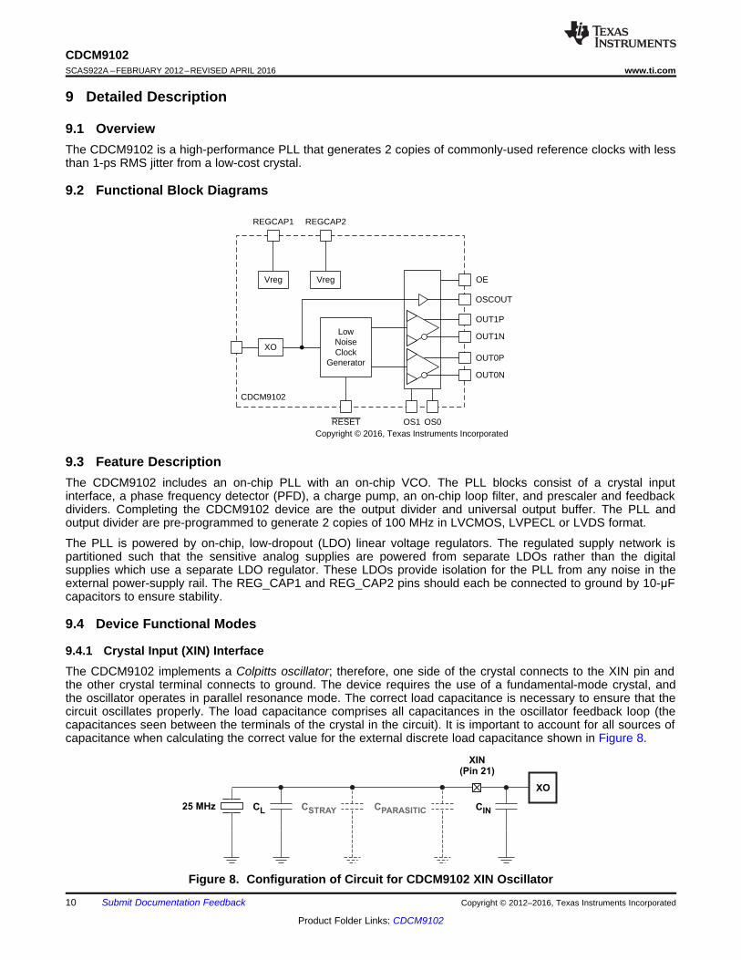
9.1 OverviewThe CDCM9102 is a high-performance PLL that generates 2 copies of commonly-used reference clocks with lessthan 1-ps RMS jitter from a low-cost crystal.
9.2 Functional Block Diagrams
9.3 Feature DescriptionThe CDCM9102 includes an on-chip PLL with an on-chip VCO. The PLL blocks consist of a crystal inputinterface, a phase frequency detector (PFD), a charge pump, an on-chip loop filter, and prescaler and feedbackdividers. Completing the CDCM9102 device are the output divider and universal output buffer. The PLL andoutput divider are pre-programmed to generate 2 copies of 100 MHz in LVCMOS, LVPECL or LVDS format.
The PLL is powered by on-chip, low-dropout (LDO) linear voltage regulators. The regulated supply network ispartitioned such that the sensitive analog supplies are powered from separate LDOs rather than the digitalsupplies which use a separate LDO regulator. These LDOs provide isolation for the PLL from any noise in theexternal power-supply rail. The REG_CAP1 and REG_CAP2 pins should each be connected to ground by 10-μFcapacitors to ensure stability.
9.4 Device Functional Modes
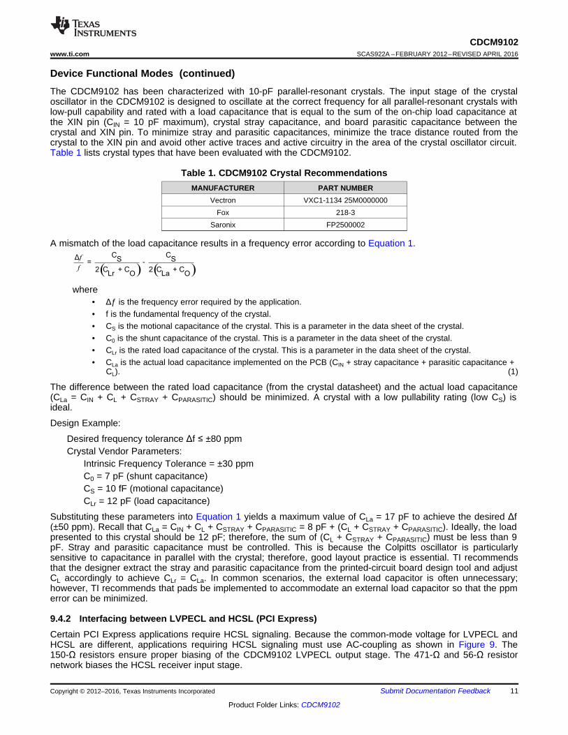
9.4.1 Crystal Input (XIN) InterfaceThe CDCM9102 implements a Colpitts oscillator; therefore, one side of the crystal connects to the XIN pin andthe other crystal terminal connects to ground. The device requires the use of a fundamental-mode crystal, andthe oscillator operates in parallel resonance mode. The correct load capacitance is necessary to ensure that thecircuit oscillates properly. The load capacitance comprises all capacitances in the oscillator feedback loop (thecapacitances seen between the terminals of the crystal in the circuit). It is important to account for all sources ofcapacitance when calculating the correct value for the external discrete load capacitance shown in Figure 8.
Figure 8. Configuration of Circuit for CDCM9102 XIN Oscillator
( ) ( )C CΔ S S
= -
2 C + C 2 C + CLr LaO O
f
f
11
CDCM9102www.ti.com SCAS922A –FEBRUARY 2012–REVISED APRIL 2016
Product Folder Links: CDCM9102
Submit Documentation FeedbackCopyright © 2012–2016, Texas Instruments Incorporated
Device Functional Modes (continued)The CDCM9102 has been characterized with 10-pF parallel-resonant crystals. The input stage of the crystaloscillator in the CDCM9102 is designed to oscillate at the correct frequency for all parallel-resonant crystals withlow-pull capability and rated with a load capacitance that is equal to the sum of the on-chip load capacitance atthe XIN pin (CIN = 10 pF maximum), crystal stray capacitance, and board parasitic capacitance between thecrystal and XIN pin. To minimize stray and parasitic capacitances, minimize the trace distance routed from thecrystal to the XIN pin and avoid other active traces and active circuitry in the area of the crystal oscillator circuit.Table 1 lists crystal types that have been evaluated with the CDCM9102.
Table 1. CDCM9102 Crystal RecommendationsMANUFACTURER PART NUMBER
Vectron VXC1-1134 25M0000000Fox 218-3
Saronix FP2500002
A mismatch of the load capacitance results in a frequency error according to Equation 1.
where• Δƒ is the frequency error required by the application.• f is the fundamental frequency of the crystal.• CS is the motional capacitance of the crystal. This is a parameter in the data sheet of the crystal.• C0 is the shunt capacitance of the crystal. This is a parameter in the data sheet of the crystal.• CLr is the rated load capacitance of the crystal. This is a parameter in the data sheet of the crystal.• CLa is the actual load capacitance implemented on the PCB (CIN + stray capacitance + parasitic capacitance +
CL). (1)
The difference between the rated load capacitance (from the crystal datasheet) and the actual load capacitance(CLa = CIN + CL + CSTRAY + CPARASITIC) should be minimized. A crystal with a low pullability rating (low CS) isideal.
Design Example:
Desired frequency tolerance Δf ≤ ±80 ppmCrystal Vendor Parameters:
Intrinsic Frequency Tolerance = ±30 ppmC0 = 7 pF (shunt capacitance)CS = 10 fF (motional capacitance)CLr = 12 pF (load capacitance)
Substituting these parameters into Equation 1 yields a maximum value of CLa = 17 pF to achieve the desired Δf(±50 ppm). Recall that CLa = CIN + CL + CSTRAY + CPARASITIC = 8 pF + (CL + CSTRAY + CPARASITIC). Ideally, the loadpresented to this crystal should be 12 pF; therefore, the sum of (CL + CSTRAY + CPARASITIC) must be less than 9pF. Stray and parasitic capacitance must be controlled. This is because the Colpitts oscillator is particularlysensitive to capacitance in parallel with the crystal; therefore, good layout practice is essential. TI recommendsthat the designer extract the stray and parasitic capacitance from the printed-circuit board design tool and adjustCL accordingly to achieve CLr = CLa. In common scenarios, the external load capacitor is often unnecessary;however, TI recommends that pads be implemented to accommodate an external load capacitor so that the ppmerror can be minimized.
9.4.2 Interfacing between LVPECL and HCSL (PCI Express)Certain PCI Express applications require HCSL signaling. Because the common-mode voltage for LVPECL andHCSL are different, applications requiring HCSL signaling must use AC-coupling as shown in Figure 9. The150-Ω resistors ensure proper biasing of the CDCM9102 LVPECL output stage. The 471-Ω and 56-Ω resistornetwork biases the HCSL receiver input stage.

LVPECL
471 (2)W
VDDHCSL
HCSL
56 (2)W150 (2)W
12
CDCM9102SCAS922A –FEBRUARY 2012–REVISED APRIL 2016 www.ti.com
Product Folder Links: CDCM9102
Submit Documentation Feedback Copyright © 2012–2016, Texas Instruments Incorporated
CIN = 8 pF (typical), 10 pF (maximum); see Electrical Characteristics.
Figure 9. Interfacing Between LVPECL and HCSL
9.5 ProgrammingTable 2 and Table 3 list the pin controls and pin configurations of the CDCM9102 output. Table 4 lists the devicereset.
9.5.1 Device Configuration
Table 2. CDCM9102 Pin Control of Output EnableOE (Pin 7) MODE DEVICE CORE OUTPUT
0 Power down Power down Hi-Z1 Normal Active Active
Table 3. CDCM9102 Pin Configuration of Output TypeCONTROL PINS
OUTPUT MODEOS1 (Pin 10) OS0 (Pin 11)
0 0 LVCMOS, OSCOUT = OFF0 1 LVDS, OSCOUT = OFF1 0 LVPECL, OSCOUT = OFF1 1 LVPECL, OSCOUT = ON
Table 4. CDCM9102 Device ResetRESET (Pin 12) OPERATING MODE DEVICE OUTPUTS
0 Device reset Hi-Z0 → 1 Clock generator calibration Hi-Z
1 Normal Active
REFREF
1t = = 0.04 μs
f
13
CDCM9102www.ti.com SCAS922A –FEBRUARY 2012–REVISED APRIL 2016
Product Folder Links: CDCM9102
Submit Documentation FeedbackCopyright © 2012–2016, Texas Instruments Incorporated
10 Application and Implementation
NOTEInformation in the following applications sections is not part of the TI componentspecification, and TI does not warrant its accuracy or completeness. TI’s customers areresponsible for determining suitability of components for their purposes. Customers shouldvalidate and test their design implementation to confirm system functionality.
10.1 Application Information
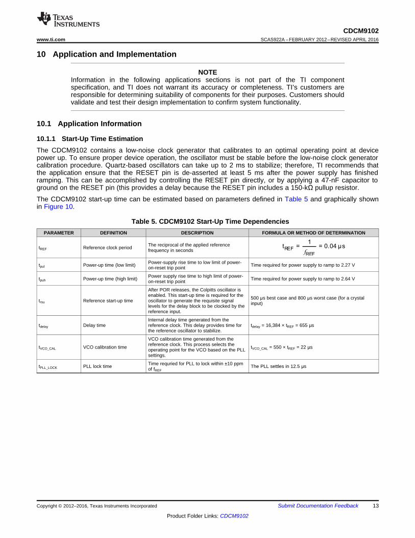
10.1.1 Start-Up Time EstimationThe CDCM9102 contains a low-noise clock generator that calibrates to an optimal operating point at devicepower up. To ensure proper device operation, the oscillator must be stable before the low-noise clock generatorcalibration procedure. Quartz-based oscillators can take up to 2 ms to stabilize; therefore, TI recommends thatthe application ensure that the RESET pin is de-asserted at least 5 ms after the power supply has finishedramping. This can be accomplished by controlling the RESET pin directly, or by applying a 47-nF capacitor toground on the RESET pin (this provides a delay because the RESET pin includes a 150-kΩ pullup resistor.
The CDCM9102 start-up time can be estimated based on parameters defined in Table 5 and graphically shownin Figure 10.
Table 5. CDCM9102 Start-Up Time DependenciesPARAMETER DEFINITION DESCRIPTION FORMULA OR METHOD OF DETERMINATION
tREF Reference clock period The reciprocal of the applied referencefrequency in seconds
tpul Power-up time (low limit) Power-supply rise time to low limit of power-on-reset trip point Time required for power supply to ramp to 2.27 V
tpuh Power-up time (high limit) Power supply rise time to high limit of power-on-reset trip point Time required for power supply to ramp to 2.64 V
trsu Reference start-up time
After POR releases, the Colpitts oscillator isenabled. This start-up time is required for theoscillator to generate the requisite signallevels for the delay block to be clocked by thereference input.
500 μs best case and 800 μs worst case (for a crystalinput)
tdelay Delay timeInternal delay time generated from thereference clock. This delay provides time forthe reference oscillator to stabilize.
tdelay = 16,384 × tREF = 655 µs
tVCO_CAL VCO calibration time
VCO calibration time generated from thereference clock. This process selects theoperating point for the VCO based on the PLLsettings.
tVCO_CAL = 550 × tREF = 22 µs
tPLL_LOCK PLL lock time Time requried for PLL to lock within ±10 ppmof fREF
The PLL settles in 12.5 μs
LVPECL LVPECL
VDDOUT
130 (2)W
82 (2)W
Po
wer
Su
pp
ly -
V
2.64
2.27
Delay VCO Calibration PLL Lock
Time - (S)tPLL_LOCKtVCO_CALtdelaytrsutpuh
tpd
Power UpReferenceStart-Up
14
CDCM9102SCAS922A –FEBRUARY 2012–REVISED APRIL 2016 www.ti.com
Product Folder Links: CDCM9102
Submit Documentation Feedback Copyright © 2012–2016, Texas Instruments Incorporated
Figure 10. CDCM9102 Start-Up Time Dependencies
The CDCM9102 start-up time limits, tMAX and tMIN, can now be calculated with Equation 2 and Equation 3.tMAX = tpuh + trsu + tdelay + tVCO_CAL + tPLL_LOCK (2)tMIN = tpul + trsu + tdelay + tVCO_CAL + tPLL_LOCK (3)
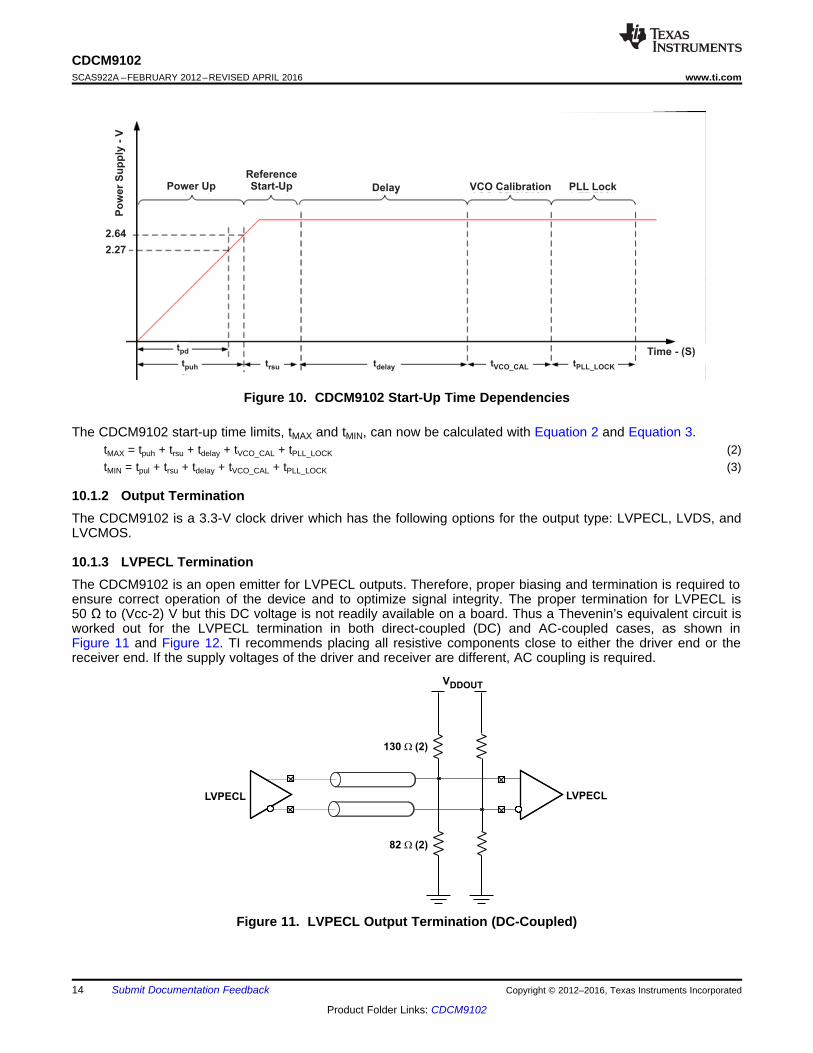
10.1.2 Output TerminationThe CDCM9102 is a 3.3-V clock driver which has the following options for the output type: LVPECL, LVDS, andLVCMOS.
10.1.3 LVPECL TerminationThe CDCM9102 is an open emitter for LVPECL outputs. Therefore, proper biasing and termination is required toensure correct operation of the device and to optimize signal integrity. The proper termination for LVPECL is50 Ω to (Vcc-2) V but this DC voltage is not readily available on a board. Thus a Thevenin’s equivalent circuit isworked out for the LVPECL termination in both direct-coupled (DC) and AC-coupled cases, as shown inFigure 11 and Figure 12. TI recommends placing all resistive components close to either the driver end or thereceiver end. If the supply voltages of the driver and receiver are different, AC coupling is required.
Figure 11. LVPECL Output Termination (DC-Coupled)
LVCMOS
22 W
LVCMOS
LVDS 100 W
LVDS LVDS100 W
LVPECL
Vb
150 (2)W
50 (2)W
15
CDCM9102www.ti.com SCAS922A –FEBRUARY 2012–REVISED APRIL 2016
Product Folder Links: CDCM9102
Submit Documentation FeedbackCopyright © 2012–2016, Texas Instruments Incorporated
Figure 12. LVPECL Output Termination (AC-Coupled)
10.1.4 LVDS TerminationThe proper LVDS termination for signal integrity over two 50-Ω lines is 100 Ω between the outputs on thereceiver end. Either a direct-coupled (dc) termination or ac-coupled termination can be used for LVDS outputs,as shown in Figure 13 and Figure 14. TI recommends placing all resistive components close to either the driverend or the receiver end. If the supply voltages of the driver and receiver are different, AC coupling is required.
Figure 13. LVDS Output Termination (DC Coupled)
Figure 14. LVDS Output Termination (AC Coupling)
10.1.5 LVCMOS TerminationSeries termination is a common method to maintain the signal integrity for LVCMOS drivers, if connected to areceiver with a high-impedance input. For series termination, a series resistor, Rs, is placed close to the driver,as shown in Figure 15. The sum of the driver impedance and Rs should be close to the transmission-lineimpedance, which is usually 50 Ω. Because the LVCMOS driver in the CDCM9102 has an impedance of 30 Ω, TIrecommends Rs be 22 Ω to maintain proper signal integrity.
Figure 15. LVCMOS Output Termination
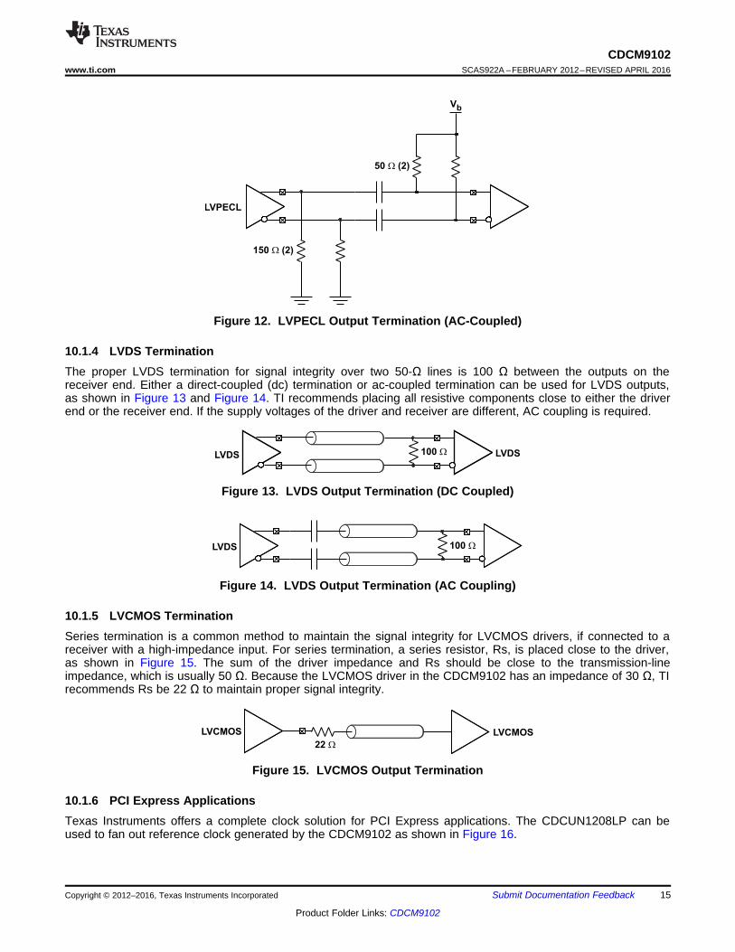
10.1.6 PCI Express ApplicationsTexas Instruments offers a complete clock solution for PCI Express applications. The CDCUN1208LP can beused to fan out reference clock generated by the CDCM9102 as shown in Figure 16.
CDCM9102
XO
LowNoiseClock
Generator
25 MHz
PCLe 100 MHz
PCLe 100 MHz
25 MHz
Copyright © 2016, Texas Instruments Incorporated
CDCM9102
100MHz LVPECL
CD
CU
N1
20
8LP
VDD
ITTP
OTTP
IN1P
IN1N25MHz
HCSL input
HCSL output
VDD
150Q 150Q 56Q 56Q
471Q 471Q
Up to 8x
100MHz
HCSL
outputs
OUT1P
OUT1N
OUT2P
OUT2N
OUT3P
OUT3N
OUT4P
OUT4N
OUT8P
OUT8N
16
CDCM9102SCAS922A –FEBRUARY 2012–REVISED APRIL 2016 www.ti.com
Product Folder Links: CDCM9102
Submit Documentation Feedback Copyright © 2012–2016, Texas Instruments Incorporated
Figure 16. Clock Solution for PCIE Express Applications
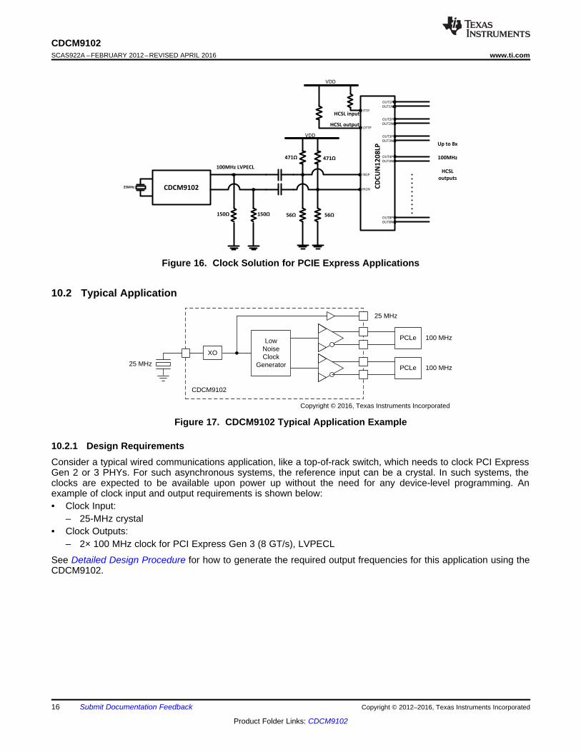
10.2 Typical Application
Figure 17. CDCM9102 Typical Application Example
10.2.1 Design RequirementsConsider a typical wired communications application, like a top-of-rack switch, which needs to clock PCI ExpressGen 2 or 3 PHYs. For such asynchronous systems, the reference input can be a crystal. In such systems, theclocks are expected to be available upon power up without the need for any device-level programming. Anexample of clock input and output requirements is shown below:• Clock Input:
– 25-MHz crystal• Clock Outputs:
– 2× 100 MHz clock for PCI Express Gen 3 (8 GT/s), LVPECL
See Detailed Design Procedure for how to generate the required output frequencies for this application using theCDCM9102.

17
CDCM9102www.ti.com SCAS922A –FEBRUARY 2012–REVISED APRIL 2016
Product Folder Links: CDCM9102
Submit Documentation FeedbackCopyright © 2012–2016, Texas Instruments Incorporated
Typical Application (continued)10.2.2 Detailed Design ProcedureDesign of all aspects of the CDCM61004 is quite involved and software support is available to assist in partselection and phase noise simulation. This design procedure will give a quick outline of the process.1. Device Selection
– The first step is to calculate the VCO frequency given the required output frequency. The device must beable to produce the VCO frequency that can be divided down to the required output frequency.
– The WEBENCH Clock Architect Tool from TI will aid in the selection of the right device that meets thecustomer's output frequencies and format requirements.
2. Device Configuration– The WEBENCH Clock Architect Tool attempts to maximize the phase detector frequency, use smallest
dividers, and maximizes PLL bandwidth.
10.2.2.1 Device SelectionUse the WEBENCH Clock Architect Tool. Enter the required frequencies and formats into the tool. To use thisdevice, find a solution using the CDCM9102.
10.2.2.1.1 Calculation Using LCM
In this example, the valid VCO frequency for CDCM9102 is 1.8 GHz.
10.2.2.2 Device ConfigurationFor this example, when using the WEBENCH Clock Architect Tool, the reference would have been manuallyentered as 25 MHz according to input frequency requirements. Enter the desired output frequencies and click onGenerate Solutions. Select CDCM9102 from the solution list.
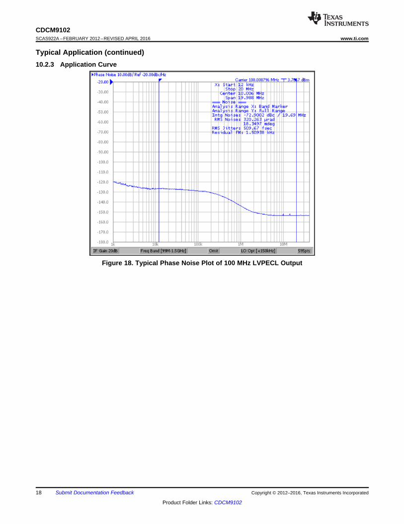
From the simulation page of the WEBENCH Clock Architect Tool, it can be seen that to maximize phase detectorfrequencies, the N divider is set to 24 and prescaler divider is set to 3. This results in a VCO frequency of1.8 GHz. The output divider is set to 6. At this point the design meets all input and output frequencyrequirements and simulate performance on the clock outputs. Figure 18 shows the typical phase noise plot of the100 MHz LVPECL output.
18
CDCM9102SCAS922A –FEBRUARY 2012–REVISED APRIL 2016 www.ti.com
Product Folder Links: CDCM9102
Submit Documentation Feedback Copyright © 2012–2016, Texas Instruments Incorporated
Typical Application (continued)10.2.3 Application Curve
Figure 18. Typical Phase Noise Plot of 100 MHz LVPECL Output
5.0 mm,min
2.1 mm, typ
0.33 mm, typ
19
CDCM9102www.ti.com SCAS922A –FEBRUARY 2012–REVISED APRIL 2016
Product Folder Links: CDCM9102
Submit Documentation FeedbackCopyright © 2012–2016, Texas Instruments Incorporated
11 Power Supply RecommendationsTA = –40°C to 85°C, VDDx = 3.3 V, OE = 1, values represent cumulative current/power on all VDDx pins.
Table 6. Device Current Consumption
BLOCK CONDITION CURRENT (mA) DEVICE POWER (mW)EXTERNALRESISTOR
POWER (mW)Entire device,core current 85 280
Output BuffersLVPECL 28 42.4 50LVDS 20 66LVCMOS V × ƒout × (CL + 20 × 10–12) × 103 V2 × ƒout × (CL + 20 × 10–12) × 103
11.1 Thermal ManagementTo ensure optimal performance and reliability, good thermal design practices are important when using theCDCM9102. Die temperature should be limited to a maximum of 125°C. That is, as an estimate, TA (ambienttemperature) plus device power consumption times RθJA should not exceed 125°C.
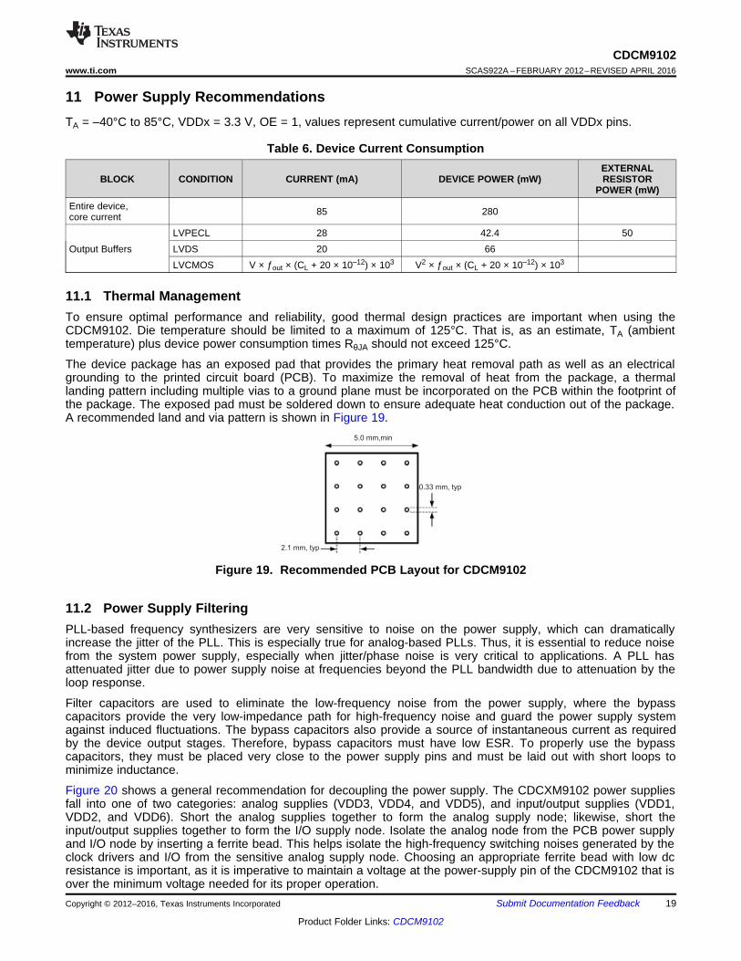
The device package has an exposed pad that provides the primary heat removal path as well as an electricalgrounding to the printed circuit board (PCB). To maximize the removal of heat from the package, a thermallanding pattern including multiple vias to a ground plane must be incorporated on the PCB within the footprint ofthe package. The exposed pad must be soldered down to ensure adequate heat conduction out of the package.A recommended land and via pattern is shown in Figure 19.
Figure 19. Recommended PCB Layout for CDCM9102
11.2 Power Supply FilteringPLL-based frequency synthesizers are very sensitive to noise on the power supply, which can dramaticallyincrease the jitter of the PLL. This is especially true for analog-based PLLs. Thus, it is essential to reduce noisefrom the system power supply, especially when jitter/phase noise is very critical to applications. A PLL hasattenuated jitter due to power supply noise at frequencies beyond the PLL bandwidth due to attenuation by theloop response.
Filter capacitors are used to eliminate the low-frequency noise from the power supply, where the bypasscapacitors provide the very low-impedance path for high-frequency noise and guard the power supply systemagainst induced fluctuations. The bypass capacitors also provide a source of instantaneous current as requiredby the device output stages. Therefore, bypass capacitors must have low ESR. To properly use the bypasscapacitors, they must be placed very close to the power supply pins and must be laid out with short loops tominimize inductance.
Figure 20 shows a general recommendation for decoupling the power supply. The CDCXM9102 power suppliesfall into one of two categories: analog supplies (VDD3, VDD4, and VDD5), and input/output supplies (VDD1,VDD2, and VDD6). Short the analog supplies together to form the analog supply node; likewise, short theinput/output supplies together to form the I/O supply node. Isolate the analog node from the PCB power supplyand I/O node by inserting a ferrite bead. This helps isolate the high-frequency switching noises generated by theclock drivers and I/O from the sensitive analog supply node. Choosing an appropriate ferrite bead with low dcresistance is important, as it is imperative to maintain a voltage at the power-supply pin of the CDCM9102 that isover the minimum voltage needed for its proper operation.

No Solder Mask
Internal
Power
Plane
Component SideBack Side
Solder Mask
Thermal Vias
QFN-32 Thermal Slug
(package bottom)
Thermal
Dissipation
Pad (back side)
Internal
Ground
Plane
Analog Node I/O NodeFerrite Bead
0.1 µF
( 3)´
0.1 µF
( 3)´
10 µF10 µF
PCBSupply
20
CDCM9102SCAS922A –FEBRUARY 2012–REVISED APRIL 2016 www.ti.com
Product Folder Links: CDCM9102
Submit Documentation Feedback Copyright © 2012–2016, Texas Instruments Incorporated
Power Supply Filtering (continued)
Figure 20. CDCM9102 Power Supply Decoupling – Power Pin Bypass Concept
12 Layout
12.1 Layout GuidelinesThe CDCM9102 is a high-performance device; therefore, pay careful attention to device configuration andprinted-circuit board layout with respect to power consumption. Observing good thermal layout practices enablesthe thermal pad on the backside of the 32-pin VQFN package to provide a good thermal path between the diecontained within the package and the ambient air. This thermal pad also serves as the ground connection thedevice; therefore, a low inductance connection to the ground plane is essential.
12.2 Layout ExampleFigure 21 shows a general recommendation of PCB layout with the CDCM9102 that ensures good system-levelthermal reliability.
Figure 21. Recommended PCB Layout
21
CDCM9102www.ti.com SCAS922A –FEBRUARY 2012–REVISED APRIL 2016
Product Folder Links: CDCM9102
Submit Documentation FeedbackCopyright © 2012–2016, Texas Instruments Incorporated
13 Device and Documentation Support
13.1 Community ResourcesThe following links connect to TI community resources. Linked contents are provided "AS IS" by the respectivecontributors. They do not constitute TI specifications and do not necessarily reflect TI's views; see TI's Terms ofUse.
TI E2E™ Online Community TI's Engineer-to-Engineer (E2E) Community. Created to foster collaborationamong engineers. At e2e.ti.com, you can ask questions, share knowledge, explore ideas and helpsolve problems with fellow engineers.
Design Support TI's Design Support Quickly find helpful E2E forums along with design support tools andcontact information for technical support.
13.2 TrademarksE2E is a trademark of Texas Instruments.PCI Express is a trademark of PCI-SIG.All other trademarks are the property of their respective owners.
13.3 Electrostatic Discharge CautionThese devices have limited built-in ESD protection. The leads should be shorted together or the device placed in conductive foamduring storage or handling to prevent electrostatic damage to the MOS gates.
13.4 GlossarySLYZ022 — TI Glossary.
This glossary lists and explains terms, acronyms, and definitions.
14 Mechanical, Packaging, and Orderable InformationThe following pages include mechanical, packaging, and orderable information. This information is the mostcurrent data available for the designated devices. This data is subject to change without notice and revision ofthis document. For browser-based versions of this data sheet, refer to the left-hand navigation.
PACKAGE OPTION ADDENDUM
www.ti.com 27-Jul-2013
Addendum-Page 1
PACKAGING INFORMATION
Orderable Device Status(1)
Package Type PackageDrawing
Pins PackageQty
Eco Plan(2)
Lead/Ball Finish MSL Peak Temp(3)
Op Temp (°C) Device Marking(4/5)
Samples
CDCM9102RHBR ACTIVE VQFN RHB 32 3000 Green (RoHS& no Sb/Br)
CU NIPDAU Level-2-260C-1 YEAR -40 to 85 CDCM9102
CDCM9102RHBT ACTIVE VQFN RHB 32 250 Green (RoHS& no Sb/Br)
CU NIPDAU Level-2-260C-1 YEAR -40 to 85 CDCM9102
(1) The marketing status values are defined as follows:ACTIVE: Product device recommended for new designs.LIFEBUY: TI has announced that the device will be discontinued, and a lifetime-buy period is in effect.NRND: Not recommended for new designs. Device is in production to support existing customers, but TI does not recommend using this part in a new design.PREVIEW: Device has been announced but is not in production. Samples may or may not be available.OBSOLETE: TI has discontinued the production of the device.
(2) Eco Plan - The planned eco-friendly classification: Pb-Free (RoHS), Pb-Free (RoHS Exempt), or Green (RoHS & no Sb/Br) - please check http://www.ti.com/productcontent for the latest availabilityinformation and additional product content details.TBD: The Pb-Free/Green conversion plan has not been defined.Pb-Free (RoHS): TI's terms "Lead-Free" or "Pb-Free" mean semiconductor products that are compatible with the current RoHS requirements for all 6 substances, including the requirement thatlead not exceed 0.1% by weight in homogeneous materials. Where designed to be soldered at high temperatures, TI Pb-Free products are suitable for use in specified lead-free processes.Pb-Free (RoHS Exempt): This component has a RoHS exemption for either 1) lead-based flip-chip solder bumps used between the die and package, or 2) lead-based die adhesive used betweenthe die and leadframe. The component is otherwise considered Pb-Free (RoHS compatible) as defined above.Green (RoHS & no Sb/Br): TI defines "Green" to mean Pb-Free (RoHS compatible), and free of Bromine (Br) and Antimony (Sb) based flame retardants (Br or Sb do not exceed 0.1% by weightin homogeneous material)
(3) MSL, Peak Temp. -- The Moisture Sensitivity Level rating according to the JEDEC industry standard classifications, and peak solder temperature.
(4) There may be additional marking, which relates to the logo, the lot trace code information, or the environmental category on the device.
(5) Multiple Device Markings will be inside parentheses. Only one Device Marking contained in parentheses and separated by a "~" will appear on a device. If a line is indented then it is a continuationof the previous line and the two combined represent the entire Device Marking for that device.
Important Information and Disclaimer:The information provided on this page represents TI's knowledge and belief as of the date that it is provided. TI bases its knowledge and belief on informationprovided by third parties, and makes no representation or warranty as to the accuracy of such information. Efforts are underway to better integrate information from third parties. TI has taken andcontinues to take reasonable steps to provide representative and accurate information but may not have conducted destructive testing or chemical analysis on incoming materials and chemicals.TI and TI suppliers consider certain information to be proprietary, and thus CAS numbers and other limited information may not be available for release.
In no event shall TI's liability arising out of such information exceed the total purchase price of the TI part(s) at issue in this document sold by TI to Customer on an annual basis.
TAPE AND REEL INFORMATION
*All dimensions are nominal
Device PackageType
PackageDrawing
Pins SPQ ReelDiameter
(mm)
ReelWidth
W1 (mm)
A0(mm)
B0(mm)
K0(mm)
P1(mm)
W(mm)
Pin1Quadrant
CDCM9102RHBR VQFN RHB 32 3000 330.0 12.4 5.3 5.3 1.5 8.0 12.0 Q2
CDCM9102RHBT VQFN RHB 32 250 180.0 12.4 5.3 5.3 1.5 8.0 12.0 Q2
PACKAGE MATERIALS INFORMATION
www.ti.com 3-Aug-2017
Pack Materials-Page 1
*All dimensions are nominal
Device Package Type Package Drawing Pins SPQ Length (mm) Width (mm) Height (mm)
CDCM9102RHBR VQFN RHB 32 3000 367.0 367.0 35.0
CDCM9102RHBT VQFN RHB 32 250 210.0 185.0 35.0
PACKAGE MATERIALS INFORMATION
www.ti.com 3-Aug-2017
Pack Materials-Page 2
IMPORTANT NOTICE
Texas Instruments Incorporated (TI) reserves the right to make corrections, enhancements, improvements and other changes to itssemiconductor products and services per JESD46, latest issue, and to discontinue any product or service per JESD48, latest issue. Buyersshould obtain the latest relevant information before placing orders and should verify that such information is current and complete.TI’s published terms of sale for semiconductor products (http://www.ti.com/sc/docs/stdterms.htm) apply to the sale of packaged integratedcircuit products that TI has qualified and released to market. Additional terms may apply to the use or sale of other types of TI products andservices.Reproduction of significant portions of TI information in TI data sheets is permissible only if reproduction is without alteration and isaccompanied by all associated warranties, conditions, limitations, and notices. TI is not responsible or liable for such reproduceddocumentation. Information of third parties may be subject to additional restrictions. Resale of TI products or services with statementsdifferent from or beyond the parameters stated by TI for that product or service voids all express and any implied warranties for theassociated TI product or service and is an unfair and deceptive business practice. TI is not responsible or liable for any such statements.Buyers and others who are developing systems that incorporate TI products (collectively, “Designers”) understand and agree that Designersremain responsible for using their independent analysis, evaluation and judgment in designing their applications and that Designers havefull and exclusive responsibility to assure the safety of Designers' applications and compliance of their applications (and of all TI productsused in or for Designers’ applications) with all applicable regulations, laws and other applicable requirements. Designer represents that, withrespect to their applications, Designer has all the necessary expertise to create and implement safeguards that (1) anticipate dangerousconsequences of failures, (2) monitor failures and their consequences, and (3) lessen the likelihood of failures that might cause harm andtake appropriate actions. Designer agrees that prior to using or distributing any applications that include TI products, Designer willthoroughly test such applications and the functionality of such TI products as used in such applications.TI’s provision of technical, application or other design advice, quality characterization, reliability data or other services or information,including, but not limited to, reference designs and materials relating to evaluation modules, (collectively, “TI Resources”) are intended toassist designers who are developing applications that incorporate TI products; by downloading, accessing or using TI Resources in anyway, Designer (individually or, if Designer is acting on behalf of a company, Designer’s company) agrees to use any particular TI Resourcesolely for this purpose and subject to the terms of this Notice.TI’s provision of TI Resources does not expand or otherwise alter TI’s applicable published warranties or warranty disclaimers for TIproducts, and no additional obligations or liabilities arise from TI providing such TI Resources. TI reserves the right to make corrections,enhancements, improvements and other changes to its TI Resources. TI has not conducted any testing other than that specificallydescribed in the published documentation for a particular TI Resource.Designer is authorized to use, copy and modify any individual TI Resource only in connection with the development of applications thatinclude the TI product(s) identified in such TI Resource. NO OTHER LICENSE, EXPRESS OR IMPLIED, BY ESTOPPEL OR OTHERWISETO ANY OTHER TI INTELLECTUAL PROPERTY RIGHT, AND NO LICENSE TO ANY TECHNOLOGY OR INTELLECTUAL PROPERTYRIGHT OF TI OR ANY THIRD PARTY IS GRANTED HEREIN, including but not limited to any patent right, copyright, mask work right, orother intellectual property right relating to any combination, machine, or process in which TI products or services are used. Informationregarding or referencing third-party products or services does not constitute a license to use such products or services, or a warranty orendorsement thereof. Use of TI Resources may require a license from a third party under the patents or other intellectual property of thethird party, or a license from TI under the patents or other intellectual property of TI.TI RESOURCES ARE PROVIDED “AS IS” AND WITH ALL FAULTS. TI DISCLAIMS ALL OTHER WARRANTIES ORREPRESENTATIONS, EXPRESS OR IMPLIED, REGARDING RESOURCES OR USE THEREOF, INCLUDING BUT NOT LIMITED TOACCURACY OR COMPLETENESS, TITLE, ANY EPIDEMIC FAILURE WARRANTY AND ANY IMPLIED WARRANTIES OFMERCHANTABILITY, FITNESS FOR A PARTICULAR PURPOSE, AND NON-INFRINGEMENT OF ANY THIRD PARTY INTELLECTUALPROPERTY RIGHTS. TI SHALL NOT BE LIABLE FOR AND SHALL NOT DEFEND OR INDEMNIFY DESIGNER AGAINST ANY CLAIM,INCLUDING BUT NOT LIMITED TO ANY INFRINGEMENT CLAIM THAT RELATES TO OR IS BASED ON ANY COMBINATION OFPRODUCTS EVEN IF DESCRIBED IN TI RESOURCES OR OTHERWISE. IN NO EVENT SHALL TI BE LIABLE FOR ANY ACTUAL,DIRECT, SPECIAL, COLLATERAL, INDIRECT, PUNITIVE, INCIDENTAL, CONSEQUENTIAL OR EXEMPLARY DAMAGES INCONNECTION WITH OR ARISING OUT OF TI RESOURCES OR USE THEREOF, AND REGARDLESS OF WHETHER TI HAS BEENADVISED OF THE POSSIBILITY OF SUCH DAMAGES.Unless TI has explicitly designated an individual product as meeting the requirements of a particular industry standard (e.g., ISO/TS 16949and ISO 26262), TI is not responsible for any failure to meet such industry standard requirements.Where TI specifically promotes products as facilitating functional safety or as compliant with industry functional safety standards, suchproducts are intended to help enable customers to design and create their own applications that meet applicable functional safety standardsand requirements. Using products in an application does not by itself establish any safety features in the application. Designers mustensure compliance with safety-related requirements and standards applicable to their applications. Designer may not use any TI products inlife-critical medical equipment unless authorized officers of the parties have executed a special contract specifically governing such use.Life-critical medical equipment is medical equipment where failure of such equipment would cause serious bodily injury or death (e.g., lifesupport, pacemakers, defibrillators, heart pumps, neurostimulators, and implantables). Such equipment includes, without limitation, allmedical devices identified by the U.S. Food and Drug Administration as Class III devices and equivalent classifications outside the U.S.TI may expressly designate certain products as completing a particular qualification (e.g., Q100, Military Grade, or Enhanced Product).Designers agree that it has the necessary expertise to select the product with the appropriate qualification designation for their applicationsand that proper product selection is at Designers’ own risk. Designers are solely responsible for compliance with all legal and regulatoryrequirements in connection with such selection.Designer will fully indemnify TI and its representatives against any damages, costs, losses, and/or liabilities arising out of Designer’s non-compliance with the terms and provisions of this Notice.
Mailing Address: Texas Instruments, Post Office Box 655303, Dallas, Texas 75265Copyright © 2017, Texas Instruments Incorporated