Embed Size (px)
Citation preview
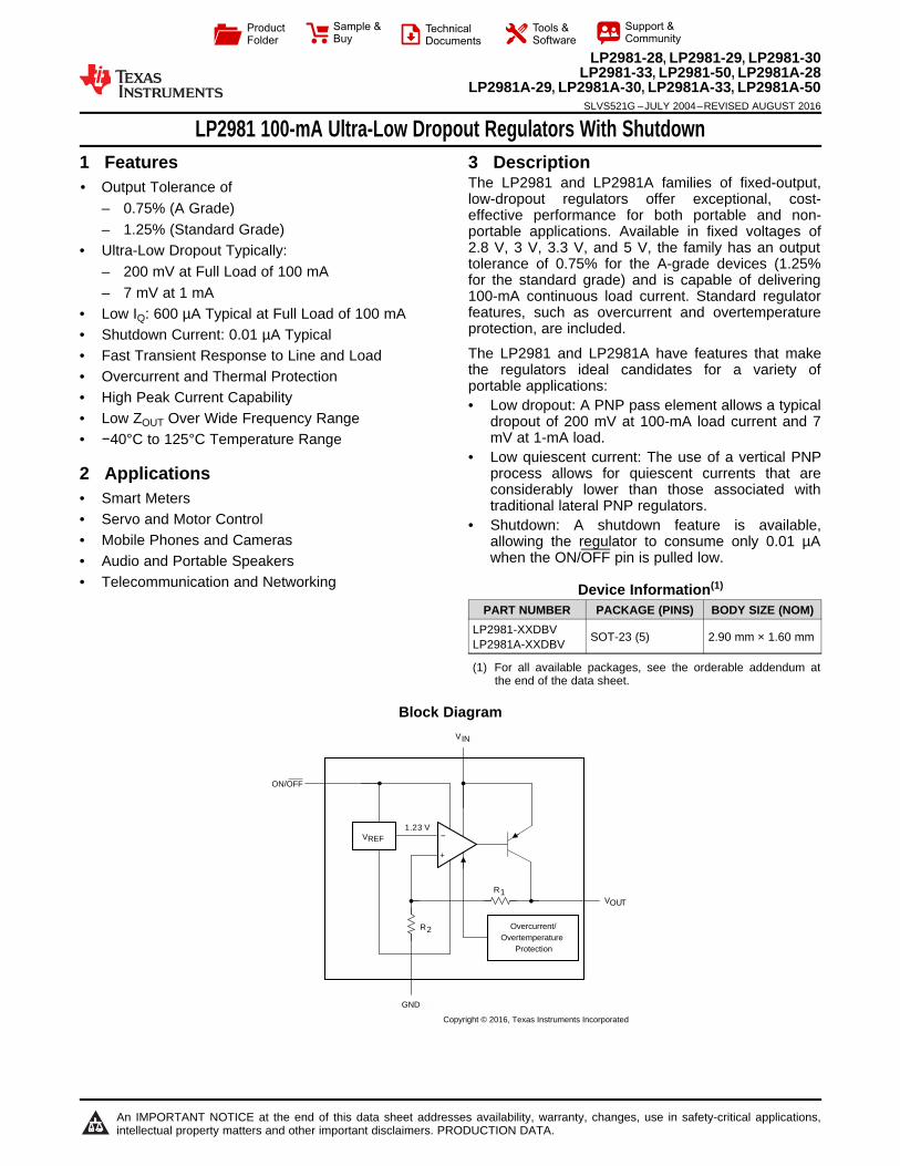
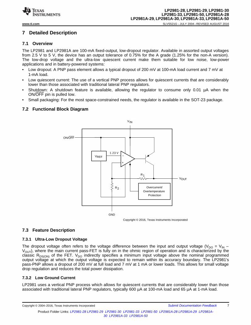
VIN
VOUT
GND
ON/OFF
VREF1.23 V
í
+
R1
R2 Overcurrent/Overtemperature
Protection
Copyright © 2016, Texas Instruments Incorporated
Product
Folder
Sample &Buy
Technical
Documents
Tools &
Software
Support &Community
An IMPORTANT NOTICE at the end of this data sheet addresses availability, warranty, changes, use in safety-critical applications,intellectual property matters and other important disclaimers. PRODUCTION DATA.
LP2981-28, LP2981-29, LP2981-30LP2981-33, LP2981-50, LP2981A-28
LP2981A-29, LP2981A-30, LP2981A-33, LP2981A-50SLVS521G –JULY 2004–REVISED AUGUST 2016
LP2981 100-mA Ultra-Low Dropout Regulators With Shutdown
1
1 Features1• Output Tolerance of
– 0.75% (A Grade)– 1.25% (Standard Grade)
• Ultra-Low Dropout Typically:– 200 mV at Full Load of 100 mA– 7 mV at 1 mA
• Low IQ: 600 µA Typical at Full Load of 100 mA• Shutdown Current: 0.01 µA Typical• Fast Transient Response to Line and Load• Overcurrent and Thermal Protection• High Peak Current Capability• Low ZOUT Over Wide Frequency Range• −40°C to 125°C Temperature Range
2 Applications• Smart Meters• Servo and Motor Control• Mobile Phones and Cameras• Audio and Portable Speakers• Telecommunication and Networking
3 DescriptionThe LP2981 and LP2981A families of fixed-output,low-dropout regulators offer exceptional, cost-effective performance for both portable and non-portable applications. Available in fixed voltages of2.8 V, 3 V, 3.3 V, and 5 V, the family has an outputtolerance of 0.75% for the A-grade devices (1.25%for the standard grade) and is capable of delivering100-mA continuous load current. Standard regulatorfeatures, such as overcurrent and overtemperatureprotection, are included.
The LP2981 and LP2981A have features that makethe regulators ideal candidates for a variety ofportable applications:• Low dropout: A PNP pass element allows a typical
dropout of 200 mV at 100-mA load current and 7mV at 1-mA load.
• Low quiescent current: The use of a vertical PNPprocess allows for quiescent currents that areconsiderably lower than those associated withtraditional lateral PNP regulators.
• Shutdown: A shutdown feature is available,allowing the regulator to consume only 0.01 µAwhen the ON/OFF pin is pulled low.
Device Information(1)
PART NUMBER PACKAGE (PINS) BODY SIZE (NOM)LP2981-XXDBVLP2981A-XXDBV SOT-23 (5) 2.90 mm × 1.60 mm
(1) For all available packages, see the orderable addendum atthe end of the data sheet.
Block Diagram
2
LP2981-28, LP2981-29, LP2981-30LP2981-33, LP2981-50, LP2981A-28LP2981A-29, LP2981A-30, LP2981A-33, LP2981A-50SLVS521G –JULY 2004–REVISED AUGUST 2016 www.ti.com
Product Folder Links: LP2981-28 LP2981-29 LP2981-30 LP2981-33 LP2981-50 LP2981A-28 LP2981A-29 LP2981A-30 LP2981A-33 LP2981A-50
Submit Documentation Feedback Copyright © 2004–2016, Texas Instruments Incorporated
Table of Contents1 Features .................................................................. 12 Applications ........................................................... 13 Description ............................................................. 14 Revision History..................................................... 25 Pin Configuration and Functions ......................... 36 Specifications......................................................... 3
6.1 Absolute Maximum Ratings ...................................... 36.2 ESD Ratings.............................................................. 36.3 Recommended Operating Conditions....................... 46.4 Thermal Information .................................................. 46.5 Electrical Characteristics: LP2981-xx ...................... 46.6 Electrical Characteristics: LP2981A-xx ..................... 56.7 Typical Characteristics .............................................. 6
7 Detailed Description .............................................. 77.1 Overview ................................................................... 77.2 Functional Block Diagram ......................................... 77.3 Feature Description................................................... 7
7.4 Device Functional Modes.......................................... 98 Application and Implementation ........................ 10
8.1 Application Information............................................ 108.2 Typical Application ................................................. 10
9 Power Supply Recommendations ...................... 1210 Layout................................................................... 12
10.1 Layout Guidelines ................................................. 1210.2 Layout Example .................................................... 12
11 Device and Documentation Support ................. 1311.1 Related Links ........................................................ 1311.2 Receiving Notification of Documentation Updates 1311.3 Community Resources.......................................... 1311.4 Trademarks ........................................................... 1311.5 Electrostatic Discharge Caution............................ 1311.6 Glossary ................................................................ 13
12 Mechanical, Packaging, and OrderableInformation ........................................................... 14
4 Revision HistoryNOTE: Page numbers for previous revisions may differ from page numbers in the current version.
Changes from Revision F (August 2008) to Revision G Page
• Added Device Information table, ESD Ratings table, Feature Description section, Device Functional Modes,Application and Implementation section, Power Supply Recommendations section, Layout section, Device andDocumentation Support section, and Mechanical, Packaging, and Orderable Information section....................................... 1
• Changed thermal table to align with JEDEC standards ......................................................................................................... 4
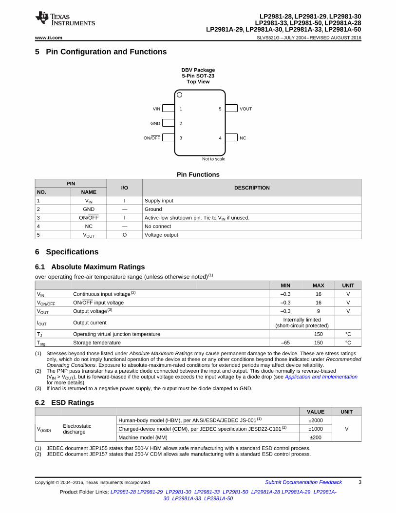
1VIN
2GND
3ON/OFF 4 NC
5 VOUT
Not to scale
3
LP2981-28, LP2981-29, LP2981-30LP2981-33, LP2981-50, LP2981A-28
LP2981A-29, LP2981A-30, LP2981A-33, LP2981A-50www.ti.com SLVS521G –JULY 2004–REVISED AUGUST 2016
Product Folder Links: LP2981-28 LP2981-29 LP2981-30 LP2981-33 LP2981-50 LP2981A-28 LP2981A-29 LP2981A-30 LP2981A-33 LP2981A-50
Submit Documentation FeedbackCopyright © 2004–2016, Texas Instruments Incorporated
5 Pin Configuration and Functions
DBV Package5-Pin SOT-23
Top View
Pin FunctionsPIN
I/O DESCRIPTIONNO. NAME1 VIN I Supply input2 GND — Ground3 ON/OFF I Active-low shutdown pin. Tie to VIN if unused.4 NC — No connect5 VOUT O Voltage output
(1) Stresses beyond those listed under Absolute Maximum Ratings may cause permanent damage to the device. These are stress ratingsonly, which do not imply functional operation of the device at these or any other conditions beyond those indicated under RecommendedOperating Conditions. Exposure to absolute-maximum-rated conditions for extended periods may affect device reliability.
(2) The PNP pass transistor has a parasitic diode connected between the input and output. This diode normally is reverse-biased(VIN > VOUT), but is forward-biased if the output voltage exceeds the input voltage by a diode drop (see Application and Implementationfor more details).
(3) If load is returned to a negative power supply, the output must be diode clamped to GND.
6 Specifications
6.1 Absolute Maximum Ratingsover operating free-air temperature range (unless otherwise noted) (1)
MIN MAX UNITVIN Continuous input voltage (2) –0.3 16 VVON/OFF ON/OFF input voltage –0.3 16 VVOUT Output voltage (3) –0.3 9 V
IOUT Output current Internally limited(short-circuit protected)
TJ Operating virtual junction temperature 150 °CTstg Storage temperature –65 150 °C
(1) JEDEC document JEP155 states that 500-V HBM allows safe manufacturing with a standard ESD control process.(2) JEDEC document JEP157 states that 250-V CDM allows safe manufacturing with a standard ESD control process.
6.2 ESD RatingsVALUE UNIT
V(ESD)Electrostaticdischarge
Human-body model (HBM), per ANSI/ESDA/JEDEC JS-001 (1) ±2000VCharged-device model (CDM), per JEDEC specification JESD22-C101 (2) ±1000
Machine model (MM) ±200
4
LP2981-28, LP2981-29, LP2981-30LP2981-33, LP2981-50, LP2981A-28LP2981A-29, LP2981A-30, LP2981A-33, LP2981A-50SLVS521G –JULY 2004–REVISED AUGUST 2016 www.ti.com
Product Folder Links: LP2981-28 LP2981-29 LP2981-30 LP2981-33 LP2981-50 LP2981A-28 LP2981A-29 LP2981A-30 LP2981A-33 LP2981A-50
Submit Documentation Feedback Copyright © 2004–2016, Texas Instruments Incorporated
(1) Minimum VIN of 2.2 V is needed for proper biasing of LDO control circuitry.
6.3 Recommended Operating ConditionsMIN MAX UNIT
VIN Supply input voltage 2.2 (1) 16 VVON/OFF ON/OFF input voltage 0 VIN VVIN – VOUT Input-output differential 0.7 11 VIOUT Output current 100 mATJ Virtual junction temperature –40 125 °C
(1) For more information about traditional and new thermal metrics, see the Semiconductor and IC Package Thermal Metrics applicationreport.
(2) Maximum power dissipation is a function of TJ(max), RθJA , and TA . The maximum allowable power dissipation at any allowable ambienttemperature is PD = (TJ(max) – TA )/ RθJA . Operating at the absolute maximum TJ of 150°C can affect reliability.
(3) The package thermal impedance is calculated in accordance with JESD 51-7.
6.4 Thermal Information
THERMAL METRIC (1)LP2981-XX
UNITDBV (SOT-23)5 PINS
RθJA Junction-to-ambient thermal resistance (2) (3) 205.2 °C/WRθJC(top) Junction-to-case (top) thermal resistance 11.83 °C/WRθJB Junction-to-board thermal resistance 37.7 °C/WψJT Junction-to-top characterization parameter 12.2 °C/WψJB Junction-to-board characterization parameter 33.8 °C/W
(1) Dropout voltage is defined as the input-to-output differential at which the output voltage drops 100 mV below the value measured with a1-V differential. This dropout specification does not apply to the 1.8-V option, as the minimum VIN = 2.2 V must be observed for properbiasing of LDO control circuitry.
6.5 Electrical Characteristics: LP2981-xxat specified free-air temperature range, VIN = VOUT(NOM) + 1 V, VON/OFF = 2 V, CIN = 1 µF, IL = 1 mA, COUT = 4.7 µF(unless otherwise noted)
PARAMETER TEST CONDITIONS TA MIN TYP MAX UNIT
ΔVOUTOutput voltagetolerance
IL = 1 mA 25°C –1.25 1.25%VNOMIL = 1 mA to 100 mA
25°C –2 2–40°C to 125°C –3.5 3.5
ΔVOUT/ΔVINOutput voltage lineregulation VIN = (VOUT(NOM) + 1 V) to 16 V
25°C 0.007 0.014%/V
–40°C to 125°C 0.032
VIN – VOUT Dropout voltage (1)
IL = 025°C 1 3
mV
–40°C to 125°C 5
IL = 1 mA25°C 7 10
–40°C to 125°C 15
IL = 25 mA25°C 70 100
–40°C to 125°C 150
IL = 100 mA25°C 200 250
–40°C to 125°C 375
5
LP2981-28, LP2981-29, LP2981-30LP2981-33, LP2981-50, LP2981A-28
LP2981A-29, LP2981A-30, LP2981A-33, LP2981A-50www.ti.com SLVS521G –JULY 2004–REVISED AUGUST 2016
Product Folder Links: LP2981-28 LP2981-29 LP2981-30 LP2981-33 LP2981-50 LP2981A-28 LP2981A-29 LP2981A-30 LP2981A-33 LP2981A-50
Submit Documentation FeedbackCopyright © 2004–2016, Texas Instruments Incorporated
Electrical Characteristics: LP2981-xx (continued)at specified free-air temperature range, VIN = VOUT(NOM) + 1 V, VON/OFF = 2 V, CIN = 1 µF, IL = 1 mA, COUT = 4.7 µF(unless otherwise noted)
PARAMETER TEST CONDITIONS TA MIN TYP MAX UNIT
(2) The ON/OFF input must be actively terminated. Connect to VIN if this function is not used (see Application and Implementation).
IGND Ground pin current
IL = 025°C 65 95
µA
–40°C to 125°C 125
IL = 1 mA25°C 80 110
–40°C to 125°C 170
IL = 25 mA25°C 200 300
–40°C to 125°C 550
IL = 100 mA25°C 600 1000
–40°C to 125°C 1700VON/OFF < 0.3 V (OFF) 25°C 0.01 0.8
VON/OFF < 0.15 V (OFF)–40°C to 105°C 0.05 2–40°C to 125°C 5
VON/OFFON/OFF inputvoltage (2)
High = O/P ON25°C 1.4
V–40°C to 125°C 1.6
Low = O/P OFF25°C 0.5
–40°C to 125°C 0.15
ION/OFFON/OFF inputcurrent
VON/OFF = 025°C 0.01
µA–40°C to 125°C –1
VON/OFF = 5 V25°C 5
–40°C to 125°C 15IOUT(PK) Peak output current VOUT ≥ VOUT(NOM) – 5% 25°C 400 mA
VnOutput noise voltage(RMS)
BW = 300 Hz to 50 kHz,COUT = 10 µF 25°C 160 µV
ΔVOUT/ΔVIN Ripple rejection f = 1 kHz, COUT = 10 µF 25°C 63 dBIOUT(MAX) Short-circuit current RL = 0 (steady state) 25°C 150 mA
(1) Dropout voltage is defined as the input-to-output differential at which the output voltage drops 100 mV below the value measured with a1-V differential. This dropout specification does not apply to the 1.8-V option, as the minimum VIN = 2.2 V must be observed for properbiasing of LDO control circuitry.
6.6 Electrical Characteristics: LP2981A-xxat specified free-air temperature range, VIN = VOUT(NOM) + 1 V, VON/OFF = 2 V, CIN = 1 µF, IL = 1 mA, COUT = 4.7 µF(unless otherwise noted)
PARAMETER TEST CONDITIONS TA MIN TYP MAX UNIT
ΔVOUTOutput voltagetolerance
IL = 1 mA 25°C –0.75 0.75%VNOMIL = 1 mA to 100 mA
25°C –1 1–40°C to 125°C –2.5 2.5
ΔVOUT/ΔVINOutput voltage lineregulation VIN = (VOUT(NOM) + 1 V) to 16 V
25°C 0.007 0.014%/V
–40°C to 125°C 0.032
VIN – VOUT Dropout voltage (1)
IL = 025°C 1 3
mV
–40°C to 125°C 5
IL = 1 mA25°C 7 10
–40°C to 125°C 15
IL = 25 mA25°C 70 100
–40°C to 125°C 150
IL = 100 mA25°C 200 250
–40°C to 125°C 375
Load Current (mA)
Out
put V
olta
ge (
V)
0 10 20 30 40 50 60 70 80 90 1003.2775
3.283.28253.285
3.28753.29
3.29253.295
3.29753.3
3.30253.305
3.30753.31
3.31253.315
D001
6
LP2981-28, LP2981-29, LP2981-30LP2981-33, LP2981-50, LP2981A-28LP2981A-29, LP2981A-30, LP2981A-33, LP2981A-50SLVS521G –JULY 2004–REVISED AUGUST 2016 www.ti.com
Product Folder Links: LP2981-28 LP2981-29 LP2981-30 LP2981-33 LP2981-50 LP2981A-28 LP2981A-29 LP2981A-30 LP2981A-33 LP2981A-50
Submit Documentation Feedback Copyright © 2004–2016, Texas Instruments Incorporated
Electrical Characteristics: LP2981A-xx (continued)at specified free-air temperature range, VIN = VOUT(NOM) + 1 V, VON/OFF = 2 V, CIN = 1 µF, IL = 1 mA, COUT = 4.7 µF(unless otherwise noted)
PARAMETER TEST CONDITIONS TA MIN TYP MAX UNIT
(2) The ON/OFF input must be actively terminated. Connect to VIN if this function is not used (see Application and Implementation).
IGND Ground pin current
IL = 025°C 65 95
µA
–40°C to 125°C 125
IL = 1 mA25°C 80 110
–40°C to 125°C 170
IL = 25 mA25°C 200 300
–40°C to 125°C 550
IL = 100 mA25°C 600 1000
–40°C to 125°C 1700VON/OFF < 0.3 V (OFF) 25°C 0.01 0.8
VON/OFF < 0.15 V (OFF)–40°C to 105°C 0.05 2–40°C to 125°C 5
VON/OFFON/OFF inputvoltage (2)
High = O/P ON25°C 1.4
V–40°C to 125°C 1.6
Low = O/P OFF25°C 0.5
–40°C to 125°C 0.15
ION/OFFON/OFF inputcurrent
VON/OFF = 025°C 0.01
µA–40°C to 125°C –1
VON/OFF = 5 V25°C 5
–40°C to 125°C 15IOUT(PK) Peak output current VOUT ≥ VOUT(NOM) – 5% 25°C 150 400 mA
VnOutput noise voltage(RMS)
BW = 300 Hz to 50 kHz,COUT = 10 µF 25°C 160 µV
ΔVOUT/ΔVIN Ripple rejection f = 1 kHz, COUT = 10 µF 25°C 63 dBIOUT(MAX) Short-circuit current RL = 0 (steady state) 25°C 150 mA
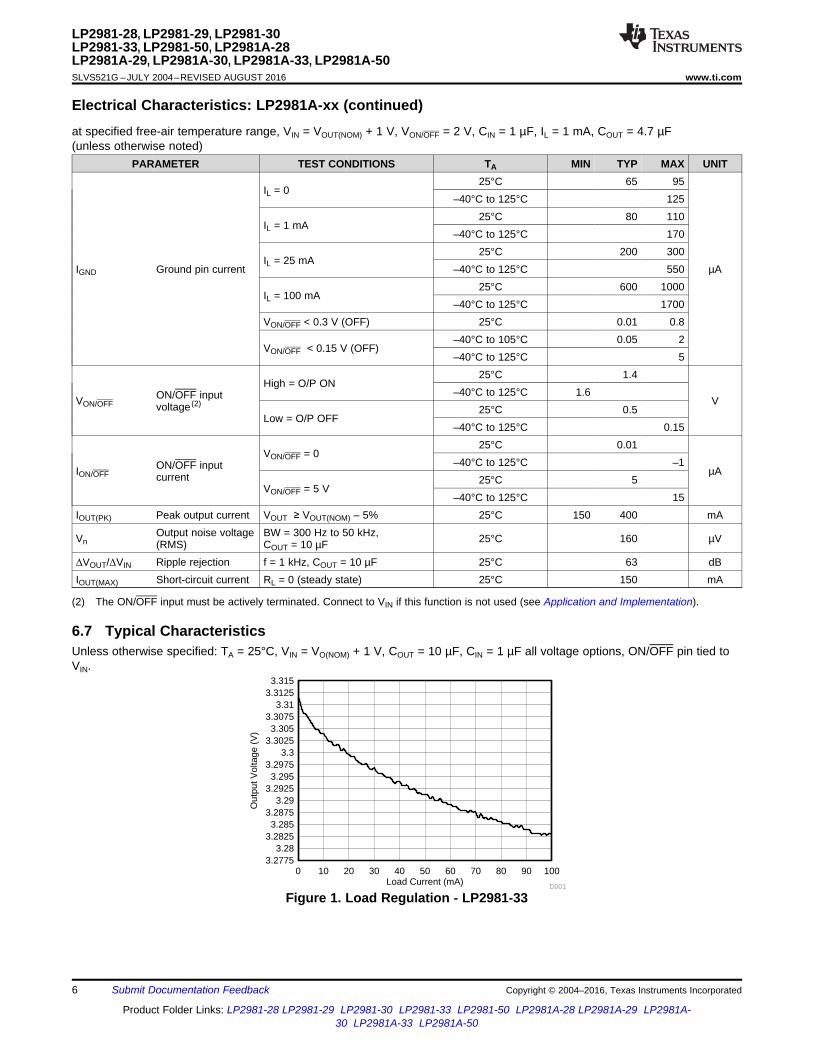
6.7 Typical CharacteristicsUnless otherwise specified: TA = 25°C, VIN = VO(NOM) + 1 V, COUT = 10 µF, CIN = 1 µF all voltage options, ON/OFF pin tied toVIN.
Figure 1. Load Regulation - LP2981-33
VIN
VOUT
GND
ON/OFF
VREF1.23 V
í
+
R1
R2 Overcurrent/Overtemperature
Protection
Copyright © 2016, Texas Instruments Incorporated
7
LP2981-28, LP2981-29, LP2981-30LP2981-33, LP2981-50, LP2981A-28
LP2981A-29, LP2981A-30, LP2981A-33, LP2981A-50www.ti.com SLVS521G –JULY 2004–REVISED AUGUST 2016
Product Folder Links: LP2981-28 LP2981-29 LP2981-30 LP2981-33 LP2981-50 LP2981A-28 LP2981A-29 LP2981A-30 LP2981A-33 LP2981A-50
Submit Documentation FeedbackCopyright © 2004–2016, Texas Instruments Incorporated
7 Detailed Description
7.1 OverviewThe LP2981 and LP2981A are 100-mA fixed-output, low-dropout regulator. Available in assorted output voltagesfrom 2.5 V to 5 V, the device has an output tolerance of 0.75% for the A grade (1.25% for the non-A version).The low-drop voltage and the ultra-low quiescent current make them suitable for low noise, low-powerapplications and in battery-powered systems:• Low dropout: A PNP pass element allows a typical dropout of 200 mV at 100-mA load current and 7 mV at
1-mA load.• Low quiescent current: The use of a vertical PNP process allows for quiescent currents that are considerably
lower than those associated with traditional lateral PNP regulators.• Shutdown: A shutdown feature is available, allowing the regulator to consume only 0.01 µA when the
ON/OFF pin is pulled low.• Small packaging: For the most space-constrained needs, the regulator is available in the SOT-23 package.
7.2 Functional Block Diagram
7.3 Feature Description
7.3.1 Ultra-Low Dropout VoltageThe dropout voltage often refers to the voltage difference between the input and output voltage (VDO = VIN –VOUT), where the main current pass-FET is fully on in the ohmic region of operation and is characterized by theclassic RDS(ON) of the FET. VDO indirectly specifies a minimum input voltage above the nominal programmedoutput voltage at which the output voltage is expected to remain within its accuracy boundary. The LP2981'spass-PNP allows a dropout of 200 mV at full load and 7 mV at 1 mA or lower loads. This allows for small voltagedrop regulation and reduces the total power dissipation.
7.3.2 Low Ground CurrentLP2981 uses a vertical PNP process which allows for quiescent currents that are considerably lower than thoseassociated with traditional lateral PNP regulators, typically 600 µA at 100-mA load and 65 µA at 1-mA load.
8
LP2981-28, LP2981-29, LP2981-30LP2981-33, LP2981-50, LP2981A-28LP2981A-29, LP2981A-30, LP2981A-33, LP2981A-50SLVS521G –JULY 2004–REVISED AUGUST 2016 www.ti.com
Product Folder Links: LP2981-28 LP2981-29 LP2981-30 LP2981-33 LP2981-50 LP2981A-28 LP2981A-29 LP2981A-30 LP2981A-33 LP2981A-50
Submit Documentation Feedback Copyright © 2004–2016, Texas Instruments Incorporated
Feature Description (continued)7.3.3 Short-Circuit Protection (Current Limit)The internal current-limit circuit is used to protect the LDO against high-load current faults or shorting events. TheLDO is not designed to operate in a steady-state current limit. During a current-limit event, the LDO sourcesconstant current. Therefore, the output voltage falls when load impedance decreases. If a current limit occursand the resulting output voltage is low, excessive power may be dissipated across the LDO resulting in a thermalshutdown of the output. A foldback feature limits the short-circuit current to protect the regulator from damageunder all load conditions. If VOUT is forced below 0 V before ON/OFF goes high and the load current requiredexceeds the foldback current limit, the device may not start up correctly.
7.3.4 Capacitor Characteristics
7.3.4.1 CeramicDue to their very low ESR values, ceramic capacitors are not suitable for use as the output capacitor. Forinstance, a typical 2.2-µF ceramic capacitor has an ESR in the range of 10 mΩ to 20 mΩ and, thus, easily canfall out of minimum ESR requirements under certain operating conditions.
If a ceramic capacitor is used at the output, a 1-Ω resistor must be placed in series with the capacitor to raise theESR seen by the regulator.
7.3.4.2 TantalumSolid tantalum capacitors are optimal choices for the LP2981, but they still must meet the minimum ESRrequirement. Note that the ESR of a tantalum capacitor increases as temperature drops, as much as doublingfrom 25°C to –40°C. Thus, ESR margins must be maintained over the temperature range to prevent regulatorinstability. For operation at very low temperatures, paralleling a tantalum capacitor with a ceramic one keeps thecombined ESR from increasing near the upper limit of the ESR curve.
7.3.4.3 AluminumAluminum capacitors can be used, but use with the LP2981 is impractical due to their large physical dimensions.They also must meet the ESR requirements over the full temperature range. In this regard, aluminium capacitorsare at a big disadvantage due to their sharp ESR increase as temperature drops. For example, over atemperature drop from 20°C to –40°C, the ESR of an aluminum electrolytic capacitor can increase by a factor of50. In addition, some of the electrolytes used in these capacitors can freeze at –25°C, making the capacitornonoperational.
VOUTVIN
Schottky
LP2981
Copyright © 2016, Texas Instruments Incorporated
VOUTVIN
9
LP2981-28, LP2981-29, LP2981-30LP2981-33, LP2981-50, LP2981A-28
LP2981A-29, LP2981A-30, LP2981A-33, LP2981A-50www.ti.com SLVS521G –JULY 2004–REVISED AUGUST 2016
Product Folder Links: LP2981-28 LP2981-29 LP2981-30 LP2981-33 LP2981-50 LP2981A-28 LP2981A-29 LP2981A-30 LP2981A-33 LP2981A-50
Submit Documentation FeedbackCopyright © 2004–2016, Texas Instruments Incorporated
7.4 Device Functional Modes
7.4.1 ON/OFF OperationThe LP2981 allows for a shutdown mode through the ON/OFF pin. If the shutdown feature is not used, ON/OFFmust be connected to the input to ensure that the regulator is on at all times. To drive ON/OFF:• A LOW (≤0.3 V) turns the regulator OFF; a HIGH (≥1.6 V) turns it ON.
– Use either a totem-pole output or an open-collector output with a pullup resistor tied to VIN (or anotherlogic supply)
• The HIGH signal can exceed VIN, but must not exceed the absolute maximum ratings of 20 V for theON/OFF pin
• Apply a signal with a slew rate of ≥40 mV/µs. A slow slew rate can cause the shutdown function to operateincorrectly
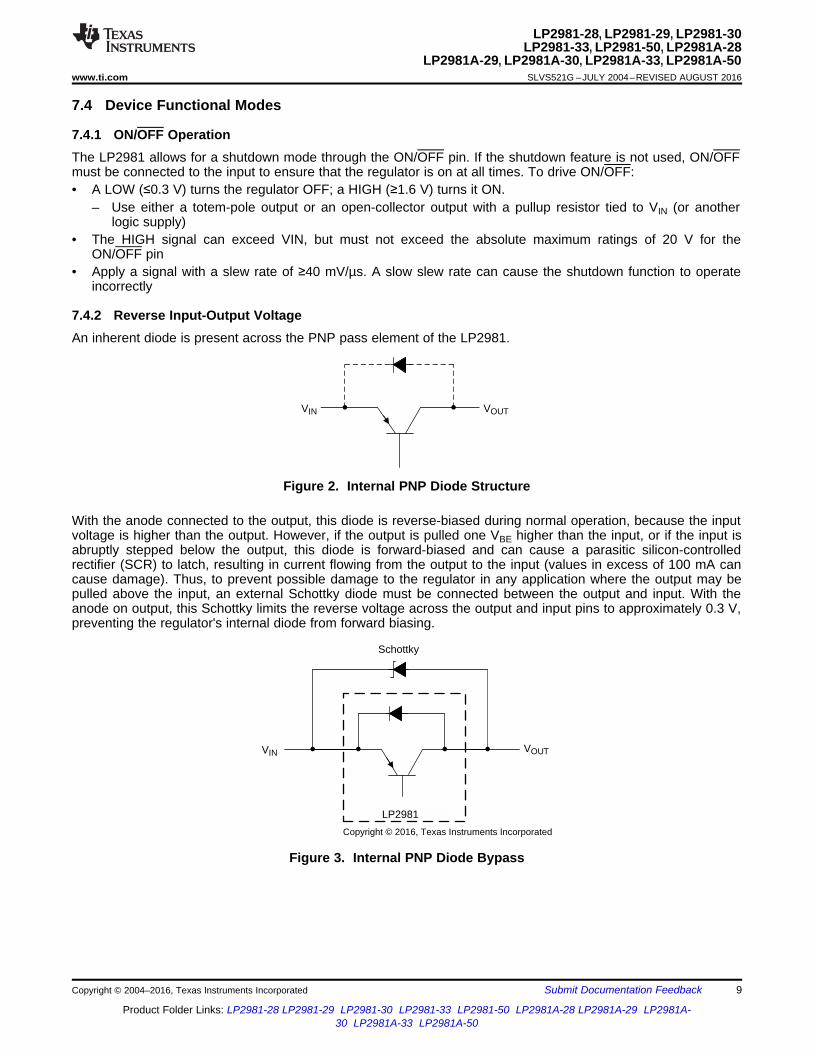
7.4.2 Reverse Input-Output VoltageAn inherent diode is present across the PNP pass element of the LP2981.
Figure 2. Internal PNP Diode Structure
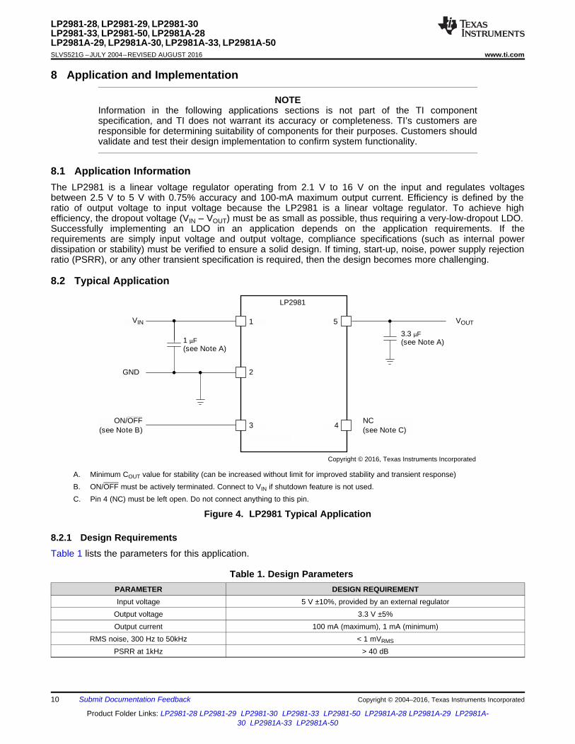
With the anode connected to the output, this diode is reverse-biased during normal operation, because the inputvoltage is higher than the output. However, if the output is pulled one VBE higher than the input, or if the input isabruptly stepped below the output, this diode is forward-biased and can cause a parasitic silicon-controlledrectifier (SCR) to latch, resulting in current flowing from the output to the input (values in excess of 100 mA cancause damage). Thus, to prevent possible damage to the regulator in any application where the output may bepulled above the input, an external Schottky diode must be connected between the output and input. With theanode on output, this Schottky limits the reverse voltage across the output and input pins to approximately 0.3 V,preventing the regulator's internal diode from forward biasing.
Figure 3. Internal PNP Diode Bypass
VOUT
3.3 F (see Note A)1 F
(see Note A)
VIN 1
ON/OFF(see Note B)
2GND
3
5
4NC(see Note C)
LP2981
Copyright © 2016, Texas Instruments Incorporated
10
LP2981-28, LP2981-29, LP2981-30LP2981-33, LP2981-50, LP2981A-28LP2981A-29, LP2981A-30, LP2981A-33, LP2981A-50SLVS521G –JULY 2004–REVISED AUGUST 2016 www.ti.com
Product Folder Links: LP2981-28 LP2981-29 LP2981-30 LP2981-33 LP2981-50 LP2981A-28 LP2981A-29 LP2981A-30 LP2981A-33 LP2981A-50
Submit Documentation Feedback Copyright © 2004–2016, Texas Instruments Incorporated
8 Application and Implementation
NOTEInformation in the following applications sections is not part of the TI componentspecification, and TI does not warrant its accuracy or completeness. TI’s customers areresponsible for determining suitability of components for their purposes. Customers shouldvalidate and test their design implementation to confirm system functionality.
8.1 Application InformationThe LP2981 is a linear voltage regulator operating from 2.1 V to 16 V on the input and regulates voltagesbetween 2.5 V to 5 V with 0.75% accuracy and 100-mA maximum output current. Efficiency is defined by theratio of output voltage to input voltage because the LP2981 is a linear voltage regulator. To achieve highefficiency, the dropout voltage (VIN – VOUT) must be as small as possible, thus requiring a very-low-dropout LDO.Successfully implementing an LDO in an application depends on the application requirements. If therequirements are simply input voltage and output voltage, compliance specifications (such as internal powerdissipation or stability) must be verified to ensure a solid design. If timing, start-up, noise, power supply rejectionratio (PSRR), or any other transient specification is required, then the design becomes more challenging.
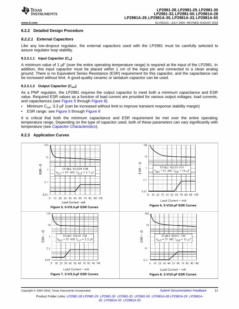
8.2 Typical Application
A. Minimum COUT value for stability (can be increased without limit for improved stability and transient response)B. ON/OFF must be actively terminated. Connect to VIN if shutdown feature is not used.C. Pin 4 (NC) must be left open. Do not connect anything to this pin.
Figure 4. LP2981 Typical Application
8.2.1 Design RequirementsTable 1 lists the parameters for this application.
Table 1. Design ParametersPARAMETER DESIGN REQUIREMENTInput voltage 5 V ±10%, provided by an external regulator
Output voltage 3.3 V ±5%Output current 100 mA (maximum), 1 mA (minimum)
RMS noise, 300 Hz to 50kHz < 1 mVRMS
PSRR at 1kHz > 40 dB
11
LP2981-28, LP2981-29, LP2981-30LP2981-33, LP2981-50, LP2981A-28
LP2981A-29, LP2981A-30, LP2981A-33, LP2981A-50www.ti.com SLVS521G –JULY 2004–REVISED AUGUST 2016
Product Folder Links: LP2981-28 LP2981-29 LP2981-30 LP2981-33 LP2981-50 LP2981A-28 LP2981A-29 LP2981A-30 LP2981A-33 LP2981A-50
Submit Documentation FeedbackCopyright © 2004–2016, Texas Instruments Incorporated
8.2.2 Detailed Design Procedure
8.2.2.1 External CapacitorsLike any low-dropout regulator, the external capacitors used with the LP2981 must be carefully selected toassure regulator loop stability.
8.2.2.1.1 Input Capacitor (Cin)
A minimum value of 1 µF (over the entire operating temperature range) is required at the input of the LP2981. Inaddition, this input capacitor must be placed within 1 cm of the input pin and connected to a clean analogground. There is no Equivalent Series Resistance (ESR) requirement for this capacitor, and the capacitance canbe increased without limit. A good-quality ceramic or tantalum capacitor can be used.
8.2.2.1.2 Output Capacitor (Cout)
As a PNP regulator, the LP2981 requires the output capacitor to meet both a minimum capacitance and ESRvalue. Required ESR values as a function of load current are provided for various output voltages, load currents,and capacitances (see Figure 5 through Figure 8).• Minimum Cout: 3.3 µF (can be increased without limit to improve transient response stability margin)• ESR range: see Figure 5 through Figure 8
It is critical that both the minimum capacitance and ESR requirement be met over the entire operatingtemperature range. Depending on the type of capacitor used, both of these parameters can vary significantly withtemperature (see Capacitor Characteristics).
8.2.3 Application Curves
Figure 5. 5-V/3.3-µF ESR Curves Figure 6. 5-V/10-µF ESR Curves
Figure 7. 3-V/3.3-µF ESR Curves Figure 8. 3-V/10-µF ESR Curves
LP2981GND
ON/OFF
IN
NC
OUTVIN
InputCapacitor
OutputCapacitor
VOUT
ON/OFF
12
LP2981-28, LP2981-29, LP2981-30LP2981-33, LP2981-50, LP2981A-28LP2981A-29, LP2981A-30, LP2981A-33, LP2981A-50SLVS521G –JULY 2004–REVISED AUGUST 2016 www.ti.com
Product Folder Links: LP2981-28 LP2981-29 LP2981-30 LP2981-33 LP2981-50 LP2981A-28 LP2981A-29 LP2981A-30 LP2981A-33 LP2981A-50
Submit Documentation Feedback Copyright © 2004–2016, Texas Instruments Incorporated
9 Power Supply RecommendationsThe LP2981 is designed to operate from an input voltage supply range between 2.2 V and 16 V. The inputvoltage range provides adequate headroom for the device to have a regulated output. This input supply must bewell regulated. If the input supply is noisy, additional input capacitors with low ESR can help improve the outputnoise performance.
10 Layout
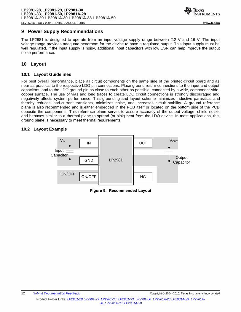
10.1 Layout GuidelinesFor best overall performance, place all circuit components on the same side of the printed-circuit board and asnear as practical to the respective LDO pin connections. Place ground return connections to the input and outputcapacitors, and to the LDO ground pin as close to each other as possible, connected by a wide, component-side,copper surface. The use of vias and long traces to create LDO circuit connections is strongly discouraged andnegatively affects system performance. This grounding and layout scheme minimizes inductive parasitics, andthereby reduces load-current transients, minimizes noise, and increases circuit stability. A ground referenceplane is also recommended and is either embedded in the PCB itself or located on the bottom side of the PCBopposite the components. This reference plane serves to assure accuracy of the output voltage, shield noise,and behaves similar to a thermal plane to spread (or sink) heat from the LDO device. In most applications, thisground plane is necessary to meet thermal requirements.
10.2 Layout Example
Figure 9. Recommended Layout
13
LP2981-28, LP2981-29, LP2981-30LP2981-33, LP2981-50, LP2981A-28
LP2981A-29, LP2981A-30, LP2981A-33, LP2981A-50www.ti.com SLVS521G –JULY 2004–REVISED AUGUST 2016
Product Folder Links: LP2981-28 LP2981-29 LP2981-30 LP2981-33 LP2981-50 LP2981A-28 LP2981A-29 LP2981A-30 LP2981A-33 LP2981A-50
Submit Documentation FeedbackCopyright © 2004–2016, Texas Instruments Incorporated
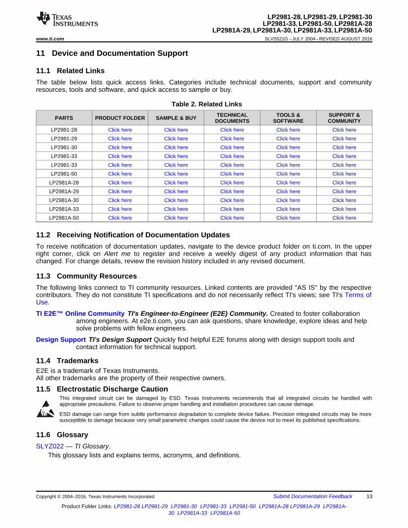
11 Device and Documentation Support
11.1 Related LinksThe table below lists quick access links. Categories include technical documents, support and communityresources, tools and software, and quick access to sample or buy.
Table 2. Related Links
PARTS PRODUCT FOLDER SAMPLE & BUY TECHNICALDOCUMENTS
TOOLS &SOFTWARE
SUPPORT &COMMUNITY
LP2981-28 Click here Click here Click here Click here Click hereLP2981-29 Click here Click here Click here Click here Click hereLP2981-30 Click here Click here Click here Click here Click hereLP2981-33 Click here Click here Click here Click here Click hereLP2981-33 Click here Click here Click here Click here Click hereLP2981-50 Click here Click here Click here Click here Click here
LP2981A-28 Click here Click here Click here Click here Click hereLP2981A-29 Click here Click here Click here Click here Click hereLP2981A-30 Click here Click here Click here Click here Click hereLP2981A-33 Click here Click here Click here Click here Click hereLP2981A-50 Click here Click here Click here Click here Click here
11.2 Receiving Notification of Documentation UpdatesTo receive notification of documentation updates, navigate to the device product folder on ti.com. In the upperright corner, click on Alert me to register and receive a weekly digest of any product information that haschanged. For change details, review the revision history included in any revised document.
11.3 Community ResourcesThe following links connect to TI community resources. Linked contents are provided "AS IS" by the respectivecontributors. They do not constitute TI specifications and do not necessarily reflect TI's views; see TI's Terms ofUse.
TI E2E™ Online Community TI's Engineer-to-Engineer (E2E) Community. Created to foster collaborationamong engineers. At e2e.ti.com, you can ask questions, share knowledge, explore ideas and helpsolve problems with fellow engineers.
Design Support TI's Design Support Quickly find helpful E2E forums along with design support tools andcontact information for technical support.
11.4 TrademarksE2E is a trademark of Texas Instruments.All other trademarks are the property of their respective owners.
11.5 Electrostatic Discharge CautionThis integrated circuit can be damaged by ESD. Texas Instruments recommends that all integrated circuits be handled withappropriate precautions. Failure to observe proper handling and installation procedures can cause damage.
ESD damage can range from subtle performance degradation to complete device failure. Precision integrated circuits may be moresusceptible to damage because very small parametric changes could cause the device not to meet its published specifications.
11.6 GlossarySLYZ022 — TI Glossary.
This glossary lists and explains terms, acronyms, and definitions.
14
LP2981-28, LP2981-29, LP2981-30LP2981-33, LP2981-50, LP2981A-28LP2981A-29, LP2981A-30, LP2981A-33, LP2981A-50SLVS521G –JULY 2004–REVISED AUGUST 2016 www.ti.com
Product Folder Links: LP2981-28 LP2981-29 LP2981-30 LP2981-33 LP2981-50 LP2981A-28 LP2981A-29 LP2981A-30 LP2981A-33 LP2981A-50
Submit Documentation Feedback Copyright © 2004–2016, Texas Instruments Incorporated
12 Mechanical, Packaging, and Orderable InformationThe following pages include mechanical, packaging, and orderable information. This information is the mostcurrent data available for the designated devices. This data is subject to change without notice and revision ofthis document. For browser-based versions of this data sheet, refer to the left-hand navigation.
PACKAGE OPTION ADDENDUM
www.ti.com 15-Apr-2017
Addendum-Page 1
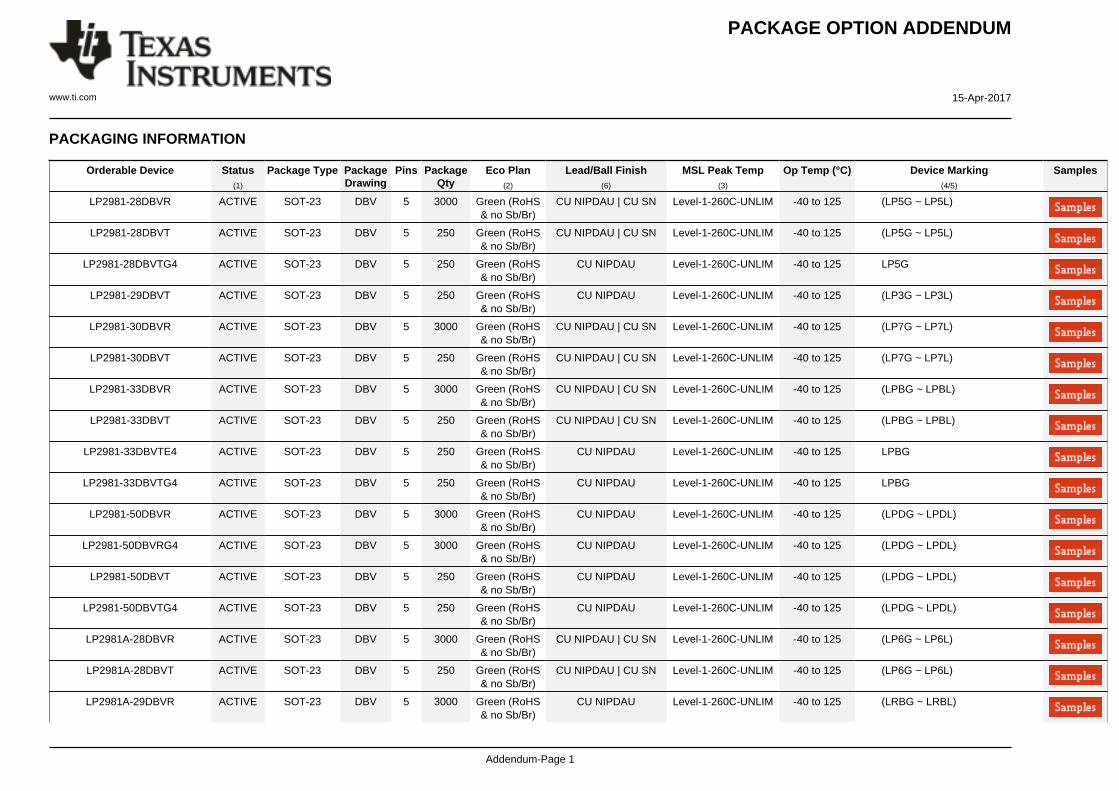
PACKAGING INFORMATION
Orderable Device Status(1)
Package Type PackageDrawing
Pins PackageQty
Eco Plan(2)
Lead/Ball Finish(6)
MSL Peak Temp(3)
Op Temp (°C) Device Marking(4/5)
Samples
LP2981-28DBVR ACTIVE SOT-23 DBV 5 3000 Green (RoHS& no Sb/Br)
CU NIPDAU | CU SN Level-1-260C-UNLIM -40 to 125 (LP5G ~ LP5L)
LP2981-28DBVT ACTIVE SOT-23 DBV 5 250 Green (RoHS& no Sb/Br)
CU NIPDAU | CU SN Level-1-260C-UNLIM -40 to 125 (LP5G ~ LP5L)
LP2981-28DBVTG4 ACTIVE SOT-23 DBV 5 250 Green (RoHS& no Sb/Br)
CU NIPDAU Level-1-260C-UNLIM -40 to 125 LP5G
LP2981-29DBVT ACTIVE SOT-23 DBV 5 250 Green (RoHS& no Sb/Br)
CU NIPDAU Level-1-260C-UNLIM -40 to 125 (LP3G ~ LP3L)
LP2981-30DBVR ACTIVE SOT-23 DBV 5 3000 Green (RoHS& no Sb/Br)
CU NIPDAU | CU SN Level-1-260C-UNLIM -40 to 125 (LP7G ~ LP7L)
LP2981-30DBVT ACTIVE SOT-23 DBV 5 250 Green (RoHS& no Sb/Br)
CU NIPDAU | CU SN Level-1-260C-UNLIM -40 to 125 (LP7G ~ LP7L)
LP2981-33DBVR ACTIVE SOT-23 DBV 5 3000 Green (RoHS& no Sb/Br)
CU NIPDAU | CU SN Level-1-260C-UNLIM -40 to 125 (LPBG ~ LPBL)
LP2981-33DBVT ACTIVE SOT-23 DBV 5 250 Green (RoHS& no Sb/Br)
CU NIPDAU | CU SN Level-1-260C-UNLIM -40 to 125 (LPBG ~ LPBL)
LP2981-33DBVTE4 ACTIVE SOT-23 DBV 5 250 Green (RoHS& no Sb/Br)
CU NIPDAU Level-1-260C-UNLIM -40 to 125 LPBG
LP2981-33DBVTG4 ACTIVE SOT-23 DBV 5 250 Green (RoHS& no Sb/Br)
CU NIPDAU Level-1-260C-UNLIM -40 to 125 LPBG
LP2981-50DBVR ACTIVE SOT-23 DBV 5 3000 Green (RoHS& no Sb/Br)
CU NIPDAU Level-1-260C-UNLIM -40 to 125 (LPDG ~ LPDL)
LP2981-50DBVRG4 ACTIVE SOT-23 DBV 5 3000 Green (RoHS& no Sb/Br)
CU NIPDAU Level-1-260C-UNLIM -40 to 125 (LPDG ~ LPDL)
LP2981-50DBVT ACTIVE SOT-23 DBV 5 250 Green (RoHS& no Sb/Br)
CU NIPDAU Level-1-260C-UNLIM -40 to 125 (LPDG ~ LPDL)
LP2981-50DBVTG4 ACTIVE SOT-23 DBV 5 250 Green (RoHS& no Sb/Br)
CU NIPDAU Level-1-260C-UNLIM -40 to 125 (LPDG ~ LPDL)
LP2981A-28DBVR ACTIVE SOT-23 DBV 5 3000 Green (RoHS& no Sb/Br)
CU NIPDAU | CU SN Level-1-260C-UNLIM -40 to 125 (LP6G ~ LP6L)
LP2981A-28DBVT ACTIVE SOT-23 DBV 5 250 Green (RoHS& no Sb/Br)
CU NIPDAU | CU SN Level-1-260C-UNLIM -40 to 125 (LP6G ~ LP6L)
LP2981A-29DBVR ACTIVE SOT-23 DBV 5 3000 Green (RoHS& no Sb/Br)
CU NIPDAU Level-1-260C-UNLIM -40 to 125 (LRBG ~ LRBL)
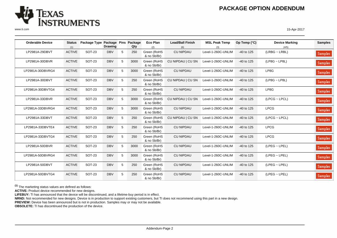
PACKAGE OPTION ADDENDUM
www.ti.com 15-Apr-2017
Addendum-Page 2
Orderable Device Status(1)
Package Type PackageDrawing
Pins PackageQty
Eco Plan(2)
Lead/Ball Finish(6)
MSL Peak Temp(3)
Op Temp (°C) Device Marking(4/5)
Samples
LP2981A-29DBVT ACTIVE SOT-23 DBV 5 250 Green (RoHS& no Sb/Br)
CU NIPDAU Level-1-260C-UNLIM -40 to 125 (LRBG ~ LRBL)
LP2981A-30DBVR ACTIVE SOT-23 DBV 5 3000 Green (RoHS& no Sb/Br)
CU NIPDAU | CU SN Level-1-260C-UNLIM -40 to 125 (LP8G ~ LP8L)
LP2981A-30DBVRG4 ACTIVE SOT-23 DBV 5 3000 Green (RoHS& no Sb/Br)
CU NIPDAU Level-1-260C-UNLIM -40 to 125 LP8G
LP2981A-30DBVT ACTIVE SOT-23 DBV 5 250 Green (RoHS& no Sb/Br)
CU NIPDAU | CU SN Level-1-260C-UNLIM -40 to 125 (LP8G ~ LP8L)
LP2981A-30DBVTG4 ACTIVE SOT-23 DBV 5 250 Green (RoHS& no Sb/Br)
CU NIPDAU Level-1-260C-UNLIM -40 to 125 LP8G
LP2981A-33DBVR ACTIVE SOT-23 DBV 5 3000 Green (RoHS& no Sb/Br)
CU NIPDAU | CU SN Level-1-260C-UNLIM -40 to 125 (LPCG ~ LPCL)
LP2981A-33DBVRG4 ACTIVE SOT-23 DBV 5 3000 Green (RoHS& no Sb/Br)
CU NIPDAU Level-1-260C-UNLIM -40 to 125 LPCG
LP2981A-33DBVT ACTIVE SOT-23 DBV 5 250 Green (RoHS& no Sb/Br)
CU NIPDAU | CU SN Level-1-260C-UNLIM -40 to 125 (LPCG ~ LPCL)
LP2981A-33DBVTE4 ACTIVE SOT-23 DBV 5 250 Green (RoHS& no Sb/Br)
CU NIPDAU Level-1-260C-UNLIM -40 to 125 LPCG
LP2981A-33DBVTG4 ACTIVE SOT-23 DBV 5 250 Green (RoHS& no Sb/Br)
CU NIPDAU Level-1-260C-UNLIM -40 to 125 LPCG
LP2981A-50DBVR ACTIVE SOT-23 DBV 5 3000 Green (RoHS& no Sb/Br)
CU NIPDAU Level-1-260C-UNLIM -40 to 125 (LPEG ~ LPEL)
LP2981A-50DBVRG4 ACTIVE SOT-23 DBV 5 3000 Green (RoHS& no Sb/Br)
CU NIPDAU Level-1-260C-UNLIM -40 to 125 (LPEG ~ LPEL)
LP2981A-50DBVT ACTIVE SOT-23 DBV 5 250 Green (RoHS& no Sb/Br)
CU NIPDAU Level-1-260C-UNLIM -40 to 125 (LPEG ~ LPEL)
LP2981A-50DBVTG4 ACTIVE SOT-23 DBV 5 250 Green (RoHS& no Sb/Br)
CU NIPDAU Level-1-260C-UNLIM -40 to 125 (LPEG ~ LPEL)
(1) The marketing status values are defined as follows:ACTIVE: Product device recommended for new designs.LIFEBUY: TI has announced that the device will be discontinued, and a lifetime-buy period is in effect.NRND: Not recommended for new designs. Device is in production to support existing customers, but TI does not recommend using this part in a new design.PREVIEW: Device has been announced but is not in production. Samples may or may not be available.OBSOLETE: TI has discontinued the production of the device.
PACKAGE OPTION ADDENDUM
www.ti.com 15-Apr-2017
Addendum-Page 3
(2) Eco Plan - The planned eco-friendly classification: Pb-Free (RoHS), Pb-Free (RoHS Exempt), or Green (RoHS & no Sb/Br) - please check http://www.ti.com/productcontent for the latest availabilityinformation and additional product content details.TBD: The Pb-Free/Green conversion plan has not been defined.Pb-Free (RoHS): TI's terms "Lead-Free" or "Pb-Free" mean semiconductor products that are compatible with the current RoHS requirements for all 6 substances, including the requirement thatlead not exceed 0.1% by weight in homogeneous materials. Where designed to be soldered at high temperatures, TI Pb-Free products are suitable for use in specified lead-free processes.Pb-Free (RoHS Exempt): This component has a RoHS exemption for either 1) lead-based flip-chip solder bumps used between the die and package, or 2) lead-based die adhesive used betweenthe die and leadframe. The component is otherwise considered Pb-Free (RoHS compatible) as defined above.Green (RoHS & no Sb/Br): TI defines "Green" to mean Pb-Free (RoHS compatible), and free of Bromine (Br) and Antimony (Sb) based flame retardants (Br or Sb do not exceed 0.1% by weightin homogeneous material)
(3) MSL, Peak Temp. - The Moisture Sensitivity Level rating according to the JEDEC industry standard classifications, and peak solder temperature.
(4) There may be additional marking, which relates to the logo, the lot trace code information, or the environmental category on the device.
(5) Multiple Device Markings will be inside parentheses. Only one Device Marking contained in parentheses and separated by a "~" will appear on a device. If a line is indented then it is a continuationof the previous line and the two combined represent the entire Device Marking for that device.
(6) Lead/Ball Finish - Orderable Devices may have multiple material finish options. Finish options are separated by a vertical ruled line. Lead/Ball Finish values may wrap to two lines if the finishvalue exceeds the maximum column width.
Important Information and Disclaimer:The information provided on this page represents TI's knowledge and belief as of the date that it is provided. TI bases its knowledge and belief on informationprovided by third parties, and makes no representation or warranty as to the accuracy of such information. Efforts are underway to better integrate information from third parties. TI has taken andcontinues to take reasonable steps to provide representative and accurate information but may not have conducted destructive testing or chemical analysis on incoming materials and chemicals.TI and TI suppliers consider certain information to be proprietary, and thus CAS numbers and other limited information may not be available for release.
In no event shall TI's liability arising out of such information exceed the total purchase price of the TI part(s) at issue in this document sold by TI to Customer on an annual basis.
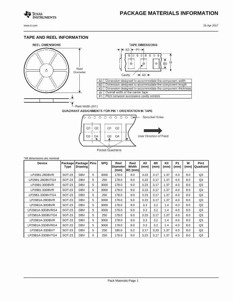
TAPE AND REEL INFORMATION
*All dimensions are nominal
Device PackageType
PackageDrawing
Pins SPQ ReelDiameter
(mm)
ReelWidth
W1 (mm)
A0(mm)
B0(mm)
K0(mm)
P1(mm)
W(mm)
Pin1Quadrant
LP2981-28DBVR SOT-23 DBV 5 3000 178.0 9.0 3.23 3.17 1.37 4.0 8.0 Q3
LP2981-28DBVTG4 SOT-23 DBV 5 250 178.0 9.0 3.23 3.17 1.37 4.0 8.0 Q3
LP2981-30DBVR SOT-23 DBV 5 3000 178.0 9.0 3.23 3.17 1.37 4.0 8.0 Q3
LP2981-33DBVR SOT-23 DBV 5 3000 178.0 9.0 3.23 3.17 1.37 4.0 8.0 Q3
LP2981-33DBVTG4 SOT-23 DBV 5 250 178.0 9.0 3.23 3.17 1.37 4.0 8.0 Q3
LP2981A-28DBVR SOT-23 DBV 5 3000 178.0 9.0 3.23 3.17 1.37 4.0 8.0 Q3
LP2981A-30DBVR SOT-23 DBV 5 3000 178.0 9.0 3.3 3.2 1.4 4.0 8.0 Q3
LP2981A-30DBVRG4 SOT-23 DBV 5 3000 178.0 9.0 3.3 3.2 1.4 4.0 8.0 Q3
LP2981A-30DBVTG4 SOT-23 DBV 5 250 178.0 9.0 3.23 3.17 1.37 4.0 8.0 Q3
LP2981A-33DBVR SOT-23 DBV 5 3000 178.0 9.0 3.3 3.2 1.4 4.0 8.0 Q3
LP2981A-33DBVRG4 SOT-23 DBV 5 3000 178.0 9.0 3.3 3.2 1.4 4.0 8.0 Q3
LP2981A-33DBVT SOT-23 DBV 5 250 180.0 9.2 3.17 3.23 1.37 4.0 8.0 Q3
LP2981A-33DBVTG4 SOT-23 DBV 5 250 178.0 9.0 3.23 3.17 1.37 4.0 8.0 Q3
PACKAGE MATERIALS INFORMATION
www.ti.com 25-Apr-2017
Pack Materials-Page 1
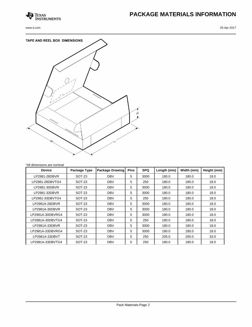
*All dimensions are nominal
Device Package Type Package Drawing Pins SPQ Length (mm) Width (mm) Height (mm)
LP2981-28DBVR SOT-23 DBV 5 3000 180.0 180.0 18.0
LP2981-28DBVTG4 SOT-23 DBV 5 250 180.0 180.0 18.0
LP2981-30DBVR SOT-23 DBV 5 3000 180.0 180.0 18.0
LP2981-33DBVR SOT-23 DBV 5 3000 180.0 180.0 18.0
LP2981-33DBVTG4 SOT-23 DBV 5 250 180.0 180.0 18.0
LP2981A-28DBVR SOT-23 DBV 5 3000 180.0 180.0 18.0
LP2981A-30DBVR SOT-23 DBV 5 3000 180.0 180.0 18.0
LP2981A-30DBVRG4 SOT-23 DBV 5 3000 180.0 180.0 18.0
LP2981A-30DBVTG4 SOT-23 DBV 5 250 180.0 180.0 18.0
LP2981A-33DBVR SOT-23 DBV 5 3000 180.0 180.0 18.0
LP2981A-33DBVRG4 SOT-23 DBV 5 3000 180.0 180.0 18.0
LP2981A-33DBVT SOT-23 DBV 5 250 205.0 200.0 33.0
LP2981A-33DBVTG4 SOT-23 DBV 5 250 180.0 180.0 18.0
PACKAGE MATERIALS INFORMATION
www.ti.com 25-Apr-2017
Pack Materials-Page 2
www.ti.com
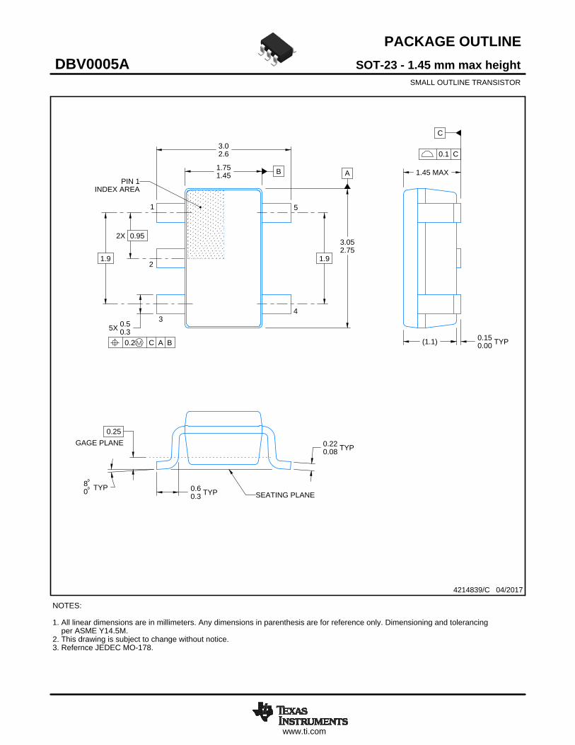
PACKAGE OUTLINE
C
TYP0.220.08
0.25
3.02.6
2X 0.95
1.9
1.45 MAX
TYP0.150.00
5X 0.50.3
TYP0.60.3
TYP80
1.9
A
3.052.75
B1.751.45
(1.1)
SOT-23 - 1.45 mm max heightDBV0005ASMALL OUTLINE TRANSISTOR
4214839/C 04/2017
NOTES: 1. All linear dimensions are in millimeters. Any dimensions in parenthesis are for reference only. Dimensioning and tolerancing per ASME Y14.5M.2. This drawing is subject to change without notice.3. Refernce JEDEC MO-178.
0.2 C A B
1
34
5
2
INDEX AREAPIN 1
GAGE PLANE
SEATING PLANE
0.1 C
SCALE 4.000

www.ti.com
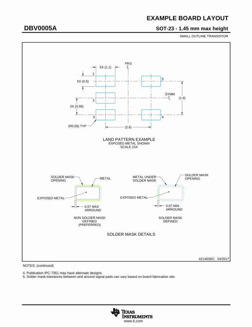
EXAMPLE BOARD LAYOUT
0.07 MAXARROUND
0.07 MINARROUND
5X (1.1)
5X (0.6)
(2.6)
(1.9)
2X (0.95)
(R0.05) TYP
4214839/C 04/2017
SOT-23 - 1.45 mm max heightDBV0005ASMALL OUTLINE TRANSISTOR
NOTES: (continued) 4. Publication IPC-7351 may have alternate designs. 5. Solder mask tolerances between and around signal pads can vary based on board fabrication site.
SYMM
LAND PATTERN EXAMPLEEXPOSED METAL SHOWN
SCALE:15X
PKG
1
3 4
5
2
SOLDER MASKOPENINGMETAL UNDER
SOLDER MASK
SOLDER MASKDEFINED
EXPOSED METAL
METALSOLDER MASKOPENING
NON SOLDER MASKDEFINED
(PREFERRED)
SOLDER MASK DETAILS
EXPOSED METAL

www.ti.com
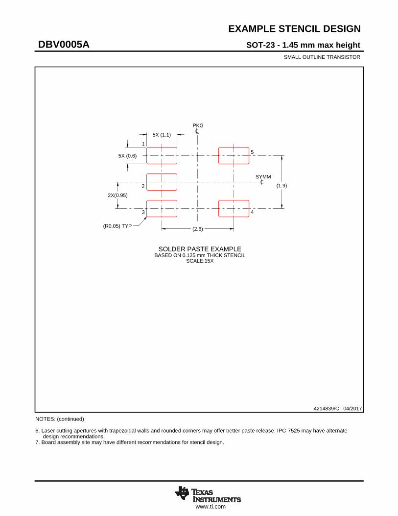
EXAMPLE STENCIL DESIGN
(2.6)
(1.9)
2X(0.95)
5X (1.1)
5X (0.6)
(R0.05) TYP
SOT-23 - 1.45 mm max heightDBV0005ASMALL OUTLINE TRANSISTOR
4214839/C 04/2017
NOTES: (continued) 6. Laser cutting apertures with trapezoidal walls and rounded corners may offer better paste release. IPC-7525 may have alternate design recommendations. 7. Board assembly site may have different recommendations for stencil design.
SOLDER PASTE EXAMPLEBASED ON 0.125 mm THICK STENCIL
SCALE:15X
SYMM
PKG
1
3 4
5
2

www.ti.com
PACKAGE OUTLINE
C
TYP0.220.08
0.25
3.02.6
2X 0.95
1.9
1.45 MAX
TYP0.150.00
5X 0.50.3
TYP0.60.3
TYP80
1.9
A
3.052.75
B1.751.45
(1.1)
SOT-23 - 1.45 mm max heightDBV0005ASMALL OUTLINE TRANSISTOR
4214839/C 04/2017
NOTES: 1. All linear dimensions are in millimeters. Any dimensions in parenthesis are for reference only. Dimensioning and tolerancing per ASME Y14.5M.2. This drawing is subject to change without notice.3. Refernce JEDEC MO-178.
0.2 C A B
1
34
5
2
INDEX AREAPIN 1
GAGE PLANE
SEATING PLANE
0.1 C
SCALE 4.000
www.ti.com
EXAMPLE BOARD LAYOUT
0.07 MAXARROUND
0.07 MINARROUND
5X (1.1)
5X (0.6)
(2.6)
(1.9)
2X (0.95)
(R0.05) TYP
4214839/C 04/2017
SOT-23 - 1.45 mm max heightDBV0005ASMALL OUTLINE TRANSISTOR
NOTES: (continued) 4. Publication IPC-7351 may have alternate designs. 5. Solder mask tolerances between and around signal pads can vary based on board fabrication site.
SYMM
LAND PATTERN EXAMPLEEXPOSED METAL SHOWN
SCALE:15X
PKG
1
3 4
5
2
SOLDER MASKOPENINGMETAL UNDER
SOLDER MASK
SOLDER MASKDEFINED
EXPOSED METAL
METALSOLDER MASKOPENING
NON SOLDER MASKDEFINED
(PREFERRED)
SOLDER MASK DETAILS
EXPOSED METAL
www.ti.com
EXAMPLE STENCIL DESIGN
(2.6)
(1.9)
2X(0.95)
5X (1.1)
5X (0.6)
(R0.05) TYP
SOT-23 - 1.45 mm max heightDBV0005ASMALL OUTLINE TRANSISTOR
4214839/C 04/2017
NOTES: (continued) 6. Laser cutting apertures with trapezoidal walls and rounded corners may offer better paste release. IPC-7525 may have alternate design recommendations. 7. Board assembly site may have different recommendations for stencil design.
SOLDER PASTE EXAMPLEBASED ON 0.125 mm THICK STENCIL
SCALE:15X
SYMM
PKG
1
3 4
5
2
IMPORTANT NOTICE
Texas Instruments Incorporated (TI) reserves the right to make corrections, enhancements, improvements and other changes to itssemiconductor products and services per JESD46, latest issue, and to discontinue any product or service per JESD48, latest issue. Buyersshould obtain the latest relevant information before placing orders and should verify that such information is current and complete.TI’s published terms of sale for semiconductor products (http://www.ti.com/sc/docs/stdterms.htm) apply to the sale of packaged integratedcircuit products that TI has qualified and released to market. Additional terms may apply to the use or sale of other types of TI products andservices.Reproduction of significant portions of TI information in TI data sheets is permissible only if reproduction is without alteration and isaccompanied by all associated warranties, conditions, limitations, and notices. TI is not responsible or liable for such reproduceddocumentation. Information of third parties may be subject to additional restrictions. Resale of TI products or services with statementsdifferent from or beyond the parameters stated by TI for that product or service voids all express and any implied warranties for theassociated TI product or service and is an unfair and deceptive business practice. TI is not responsible or liable for any such statements.Buyers and others who are developing systems that incorporate TI products (collectively, “Designers”) understand and agree that Designersremain responsible for using their independent analysis, evaluation and judgment in designing their applications and that Designers havefull and exclusive responsibility to assure the safety of Designers' applications and compliance of their applications (and of all TI productsused in or for Designers’ applications) with all applicable regulations, laws and other applicable requirements. Designer represents that, withrespect to their applications, Designer has all the necessary expertise to create and implement safeguards that (1) anticipate dangerousconsequences of failures, (2) monitor failures and their consequences, and (3) lessen the likelihood of failures that might cause harm andtake appropriate actions. Designer agrees that prior to using or distributing any applications that include TI products, Designer willthoroughly test such applications and the functionality of such TI products as used in such applications.TI’s provision of technical, application or other design advice, quality characterization, reliability data or other services or information,including, but not limited to, reference designs and materials relating to evaluation modules, (collectively, “TI Resources”) are intended toassist designers who are developing applications that incorporate TI products; by downloading, accessing or using TI Resources in anyway, Designer (individually or, if Designer is acting on behalf of a company, Designer’s company) agrees to use any particular TI Resourcesolely for this purpose and subject to the terms of this Notice.TI’s provision of TI Resources does not expand or otherwise alter TI’s applicable published warranties or warranty disclaimers for TIproducts, and no additional obligations or liabilities arise from TI providing such TI Resources. TI reserves the right to make corrections,enhancements, improvements and other changes to its TI Resources. TI has not conducted any testing other than that specificallydescribed in the published documentation for a particular TI Resource.Designer is authorized to use, copy and modify any individual TI Resource only in connection with the development of applications thatinclude the TI product(s) identified in such TI Resource. NO OTHER LICENSE, EXPRESS OR IMPLIED, BY ESTOPPEL OR OTHERWISETO ANY OTHER TI INTELLECTUAL PROPERTY RIGHT, AND NO LICENSE TO ANY TECHNOLOGY OR INTELLECTUAL PROPERTYRIGHT OF TI OR ANY THIRD PARTY IS GRANTED HEREIN, including but not limited to any patent right, copyright, mask work right, orother intellectual property right relating to any combination, machine, or process in which TI products or services are used. Informationregarding or referencing third-party products or services does not constitute a license to use such products or services, or a warranty orendorsement thereof. Use of TI Resources may require a license from a third party under the patents or other intellectual property of thethird party, or a license from TI under the patents or other intellectual property of TI.TI RESOURCES ARE PROVIDED “AS IS” AND WITH ALL FAULTS. TI DISCLAIMS ALL OTHER WARRANTIES ORREPRESENTATIONS, EXPRESS OR IMPLIED, REGARDING RESOURCES OR USE THEREOF, INCLUDING BUT NOT LIMITED TOACCURACY OR COMPLETENESS, TITLE, ANY EPIDEMIC FAILURE WARRANTY AND ANY IMPLIED WARRANTIES OFMERCHANTABILITY, FITNESS FOR A PARTICULAR PURPOSE, AND NON-INFRINGEMENT OF ANY THIRD PARTY INTELLECTUALPROPERTY RIGHTS. TI SHALL NOT BE LIABLE FOR AND SHALL NOT DEFEND OR INDEMNIFY DESIGNER AGAINST ANY CLAIM,INCLUDING BUT NOT LIMITED TO ANY INFRINGEMENT CLAIM THAT RELATES TO OR IS BASED ON ANY COMBINATION OFPRODUCTS EVEN IF DESCRIBED IN TI RESOURCES OR OTHERWISE. IN NO EVENT SHALL TI BE LIABLE FOR ANY ACTUAL,DIRECT, SPECIAL, COLLATERAL, INDIRECT, PUNITIVE, INCIDENTAL, CONSEQUENTIAL OR EXEMPLARY DAMAGES INCONNECTION WITH OR ARISING OUT OF TI RESOURCES OR USE THEREOF, AND REGARDLESS OF WHETHER TI HAS BEENADVISED OF THE POSSIBILITY OF SUCH DAMAGES.Unless TI has explicitly designated an individual product as meeting the requirements of a particular industry standard (e.g., ISO/TS 16949and ISO 26262), TI is not responsible for any failure to meet such industry standard requirements.Where TI specifically promotes products as facilitating functional safety or as compliant with industry functional safety standards, suchproducts are intended to help enable customers to design and create their own applications that meet applicable functional safety standardsand requirements. Using products in an application does not by itself establish any safety features in the application. Designers mustensure compliance with safety-related requirements and standards applicable to their applications. Designer may not use any TI products inlife-critical medical equipment unless authorized officers of the parties have executed a special contract specifically governing such use.Life-critical medical equipment is medical equipment where failure of such equipment would cause serious bodily injury or death (e.g., lifesupport, pacemakers, defibrillators, heart pumps, neurostimulators, and implantables). Such equipment includes, without limitation, allmedical devices identified by the U.S. Food and Drug Administration as Class III devices and equivalent classifications outside the U.S.TI may expressly designate certain products as completing a particular qualification (e.g., Q100, Military Grade, or Enhanced Product).Designers agree that it has the necessary expertise to select the product with the appropriate qualification designation for their applicationsand that proper product selection is at Designers’ own risk. Designers are solely responsible for compliance with all legal and regulatoryrequirements in connection with such selection.Designer will fully indemnify TI and its representatives against any damages, costs, losses, and/or liabilities arising out of Designer’s non-compliance with the terms and provisions of this Notice.
Mailing Address: Texas Instruments, Post Office Box 655303, Dallas, Texas 75265Copyright © 2018, Texas Instruments Incorporated