Embed Size (px)
Citation preview

Memec Spartan-3 LC User�s Guide
June 14, 2004Version 2.0
1
Memec Spartan-3 LC User�s Guide v2.0 June 14, 2004
www.memec.com/xilinxkits 2 [email protected]
Table of Contents
Overview............................................................................................................................. 4 Spartan-3 LC Development Board...................................................................................... 4 Spartan-3 LC Development Board Block Diagram............................................................ 6
Spartan-3 Device............................................................................................................. 6 Clock Generation ............................................................................................................ 7 User Interfaces ................................................................................................................ 8
User 7-Segment LED Display .................................................................................... 8 User LED .................................................................................................................... 9 User Push Buttons....................................................................................................... 9 User DIP Switch ......................................................................................................... 9
RS232 Port .................................................................................................................... 10 USB Port ....................................................................................................................... 11
Driver Installation ..................................................................................................... 12 Calculating the Baud Clock ...................................................................................... 16
Configuration Support .................................................................................................. 18 JTAG Port ................................................................................................................. 18 Platform Flash ISP PROM........................................................................................ 18
Maintaining 3.3V On VCCO Bank4 ....................................................................... 19 Program Switch (SW2)......................................................................................... 20 Mode Select .......................................................................................................... 20
SystemACE Connector ............................................................................................. 20 P160 Expansion Slot ..................................................................................................... 24 Power System Design ................................................................................................... 26
Revision History ............................................................................................................... 29 Contact Information .......................................................................................................... 29
Email ............................................................................................................................. 29 Telephone...................................................................................................................... 29 Web............................................................................................................................... 29
Memec Spartan-3 LC User�s Guide v2.0 June 14, 2004
www.memec.com/xilinxkits 3 [email protected]
Figures Figure 1 � Spartan-3 LC Development Board .................................................................... 5 Figure 2 � Spartan-3 LC Development Board Jumpers...................................................... 5 Figure 3 � Spartan-3 LC Block Diagram............................................................................ 6 Figure 4 � 7-Segment LED Display Interface .................................................................... 8 Figure 5 � User DIP Switch Interface............................................................................... 10 Figure 6 � RS232 Interface ............................................................................................... 10 Figure 7 � Launching CP2101 Driver Installation............................................................ 12 Figure 8 � Cygnal License Agreement ............................................................................. 13 Figure 9 � CP2101 Destination Location.......................................................................... 13 Figure 10 � CP2101 Installation Successful ..................................................................... 14 Figure 11 � Found New Hardware Wizard....................................................................... 15 Figure 12 � Windows Logo Testing Not Passed .............................................................. 15 Figure 13 � CP2101 Driver Installation Complete ........................................................... 16 Figure 14 � CP2101 Recognized as COM Port ................................................................ 16 Figure 15 � JTAG Chain Description ............................................................................... 18 Figure 16 � Platform Flash Interface ................................................................................ 19 Figure 17 � Configuration Voltage Interface.................................................................... 20 Figure 18 � SystemACE Module Plugged In ................................................................... 21 Figure 19 � SystemACE Module Block Diagram ........................................................... 22 Figure 20 � Power-up Ramp: 2.5V................................................................................... 27 Figure 21 � Power-up Ramp: 1.2V................................................................................... 28 Figure 22 � Power-up Ramp: 3.3V................................................................................... 28
Tables Table 1 � JP30 Configuration ............................................................................................. 7 Table 2 � Spartan-3 LC Board Clock ................................................................................. 8 Table 3 � 7-Segment Display Signal Descriptions (DD1).................................................. 8 Table 4 � User LED Signal Descriptions (DS3, DS4, DS7, DS8)...................................... 9 Table 5 � User Push Button Signal Descriptions (SW4 and SW5) .................................... 9 Table 6 � User DIP Switch Signal Descriptions (SW3) ................................................... 10 Table 7 � RS232 Signal Descriptions ............................................................................... 10 Table 8 � USB UART Signal Descriptions ...................................................................... 11 Table 9 � Spartan-3 Configuration Mode Select .............................................................. 20 Table 10 � SystemACE Controller Clock Source............................................................. 23 Table 11 � SystemACE Connector Signal Description .................................................... 23 Table 12 � JX1 Signal Assignments ................................................................................. 24 Table 13 � JX2 Signal Assignments ................................................................................. 25
Memec Spartan-3 LC User�s Guide v2.0 June 14, 2004
www.memec.com/xilinxkits 4 [email protected]
Overview The Spartan-3 LC Development Kit provides an easy-to-use, low cost evaluation platform for developing designs and applications based on the Xilinx Spartan-3 FPGA family. The kit bundles a versatile Spartan-3 demonstration board with a power supply, a P4-to-P3 cable adapter, user guide, and reference designs. P160 expansion modules available from Memec Design enable further application specific prototyping and testing. Several alternative kit bundles are available which include one or more of the following: Memec Design JTAG programming cable, Xilinx ISE WebPACK software CD, Xilinx EDK software, serial cable, P160 Proto module, and P160 Communications module. Please visit the Memec website or speak with a Memec salesperson regarding available bundles and pricing. The Spartan-3 LC development board utilizes the 400K-gate Xilinx Spartan-3 device (XC3S400-4PQ208CES) in the 208-pin quad flat-pack package. The 3S400 FPGA allows designers to become familiar with advanced 90-nm process performance and features. The development board includes a 50 MHz clock, a user clock socket, 29 user I/O header pins, an RS-232 port, a USB 2.0 slave port, LEDs, switches, and additional user support circuits. The board supports the Memec P160 expansion module standard, which allows application-specific expansion modules to be easily added. A SystemACE� interface on the board gives software designers the ability to create file systems on removable CompactFlash cards when implementing embedded processor solutions. The Spartan-3 FPGA family has many advanced features, including hardware multipliers, 18Kb memories, digitally-controlled I/O impedance, and sophisticated clock management hardware (including frequency synthesis, phase-shifted, and de-skewing). These features make Spartan-3 well-suited for the most demanding, high volume applications. The Memec Design Spartan-3 LC Development Kit provides an excellent platform to explore these features, enabling designers to quickly and effectively meet time-to-market requirements.
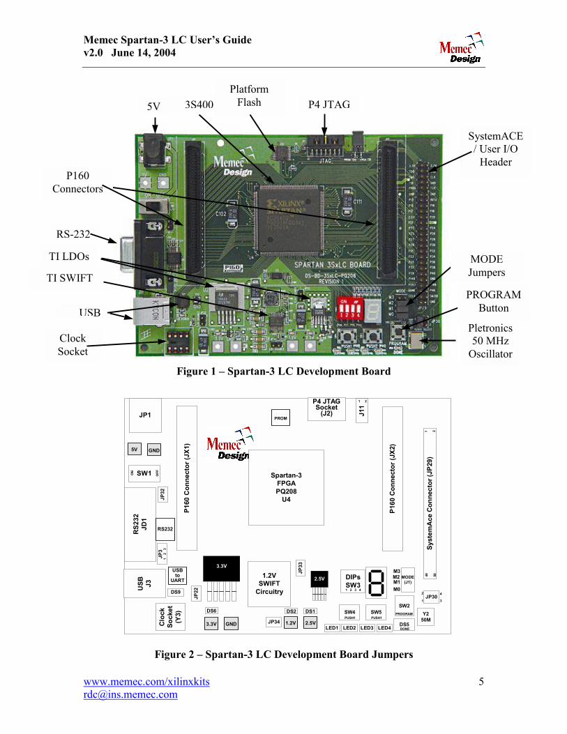
Spartan-3 LC Development Board A photograph of the Spartan-3 LC Rev 1 development board is shown in Figure 1. Various features and circuits are pointed out. A diagram is shown in Figure 2 which shows the reference designators for all of the jumpers discussed in this User�s Guide.
Memec Spartan-3 LC User�s Guide v2.0 June 14, 2004
www.memec.com/[email protected]
JP1
RS2
32JD
1
Clo
ckSo
cket
5V GND
RS232
SW1ON
OFF
USB J3
U
U
D
JP32
JP3
12
3
Figu
0 Platform
Flash
Clock Socket
TI LDOs
P160 Connectors
U
TI SWIFT
3S40
5VSystemACE / User I/O
Header
RS-232
linxkits
Figure 1 � Spartan-3 LC D
DS2
(Y3)
JP22
3.3V
1.2VSWIFT
Circuitry
1
156157
208
3.3V
GND 1.2V
SBtoART
S9
JP34
P160
Con
nect
or (J
X1)
DS6
PROM
Spartan-3FPGAPQ208
U4
re 2 � Spartan-3 LC Devel
P4 JTAG
PROGRAM Button
MODE Jumpers
SB
5
evelopment Board
P4 JTAGSocket
(J2)
LED1
JP30
DS1
2.5V
SW4PUSH1
5253
104105
DS5DONE
SW2PROGRAM
J11
1 2
MODE(J1)M1
M0
M2M3
SW5PUSH1
LED2 LED3 LED4
DIPsSW31 2 3 4
JP33
2.5V
Syst
emA
ce C
onne
ctor
(JP2
9)1 2
49 50
P160
Con
nect
or (J
X2)
Y250M
1 3
42
opment Board Jumpers
Pletronics50 MHz
Oscillator
Memec Spartan-3 LC User�s Guide v2.0 June 14, 2004
www.memec.com/xilinxkits 6 [email protected]
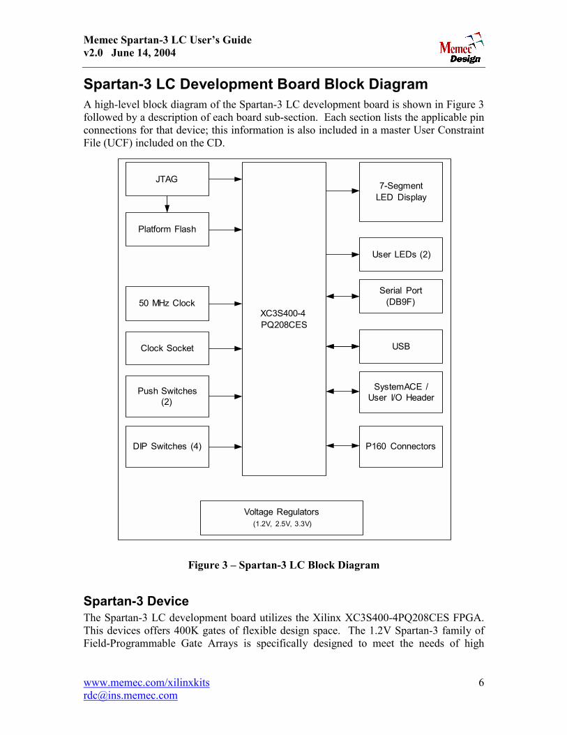
Spartan-3 LC Development Board Block Diagram A high-level block diagram of the Spartan-3 LC development board is shown in Figure 3 followed by a description of each board sub-section. Each section lists the applicable pin connections for that device; this information is also included in a master User Constraint File (UCF) included on the CD.
XC3S400-4PQ208CES
7-SegmentLED Display
User LEDs (2)
Serial Port(DB9F)
DIP Switches (4)
USB
P160 Connectors
Push Switches(2)
Clock Socket
Platform Flash
JTAG
Voltage Regulators(1.2V, 2.5V, 3.3V)
SystemACE /User I/O Header
50 MHz Clock
Figure 3 � Spartan-3 LC Block Diagram
Spartan-3 Device The Spartan-3 LC development board utilizes the Xilinx XC3S400-4PQ208CES FPGA. This devices offers 400K gates of flexible design space. The 1.2V Spartan-3 family of Field-Programmable Gate Arrays is specifically designed to meet the needs of high
Memec Spartan-3 LC User�s Guide v2.0 June 14, 2004
www.memec.com/xilinxkits 7 [email protected]
volume, cost-sensitive consumer electronic applications. The eight-member family offers densities ranging from 50K to 5M system gates. The Spartan-3 family builds on the success of the earlier Spartan-IIE family by increasing the amount of logic resources, the total number of I/Os, and the overall level of performance. Numerous additional enhancements are inherited from state-of-the-art Virtex-II� technology, including 18Kb internal BlockRAM, embedded 18x18 hardware multipliers, enhanced I/O (such as DCI, DDR registers, and additional I/O standards), and advanced clock management functions (like frequency synthesis and phase-shifting). These Spartan-3 enhancements, combined with advanced process technology, deliver more functionality and bandwidth per dollar than was previously possible, setting new standards in the programmable logic industry. Because of exceptionally low cost, Spartan-3 FPGAs are ideally suited to a wide range of consumer electronics applications, including broadband access, home networking, display/projection, and digital television equipment. The Spartan-3 family is a superior alternative to mask programmed ASICs. FPGAs avoid the high initial cost, the lengthy development cycles, and the inherent inflexibility of conventional ASICs. Also, FPGA programmability permits design upgrades in the field with no hardware replacement necessary, an impossibility with ASICs.
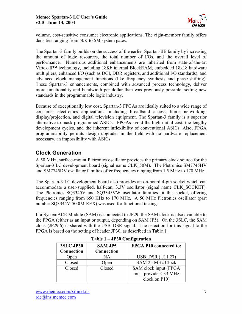
Clock Generation A 50 MHz, surface-mount Pletronics oscillator provides the primary clock source for the Spartan-3 LC development board (signal name CLK_50M). The Pletronics SM7745HV and SM7745DV oscillator families offer frequencies ranging from 1.5 MHz to 170 MHz. The Spartan-3 LC development board also provides an on-board 4-pin socket which can accommodate a user-supplied, half-can, 3.3V oscillator (signal name CLK_SOCKET). The Pletronics SQ3345V and SQ3345VW oscillator families fit this socket, offering frequencies ranging from 650 KHz to 170 MHz. A 50 MHz Pletronics oscillator (part number SQ3345V-50.0M-REX) was used for functional testing. If a SystemACE Module (SAM) is connected to JP29, the SAM clock is also available to the FPGA (either as an input or output, depending on SAM JP5). On the 3SLC, the SAM clock (JP29.6) is shared with the USB_DSR signal. The selection for this signal to the FPGA is based on the setting of header JP30, as described in Table 1.
Table 1 � JP30 Configuration 3SLC JP30 Connection
SAM JP5 Connection
FPGA P10 connected to:
Open NA USB_DSR (U11.27) Closed Open SAM 25 MHz Clock Closed Closed SAM clock input (FPGA
must provide < 33 MHz clock on P10)
Memec Spartan-3 LC User�s Guide v2.0 June 14, 2004
www.memec.com/xilinxkits 8 [email protected]
The FPGA clock pin-out is shown in Table 2.
Table 2 � Spartan-3 LC Board Clock Signal Name Spartan-3 Pin # Direction Description
CLK_50M P184 Input 50MHz oscillator CLK_SOCKET P183 Input 3.3V oscillator socket USB_DSR P10 Input or
Output Optional connection to SAM clock
User Interfaces For simple feedback and user interaction, the Spartan-3 LC development board provides several user interfaces, described in the following sections:
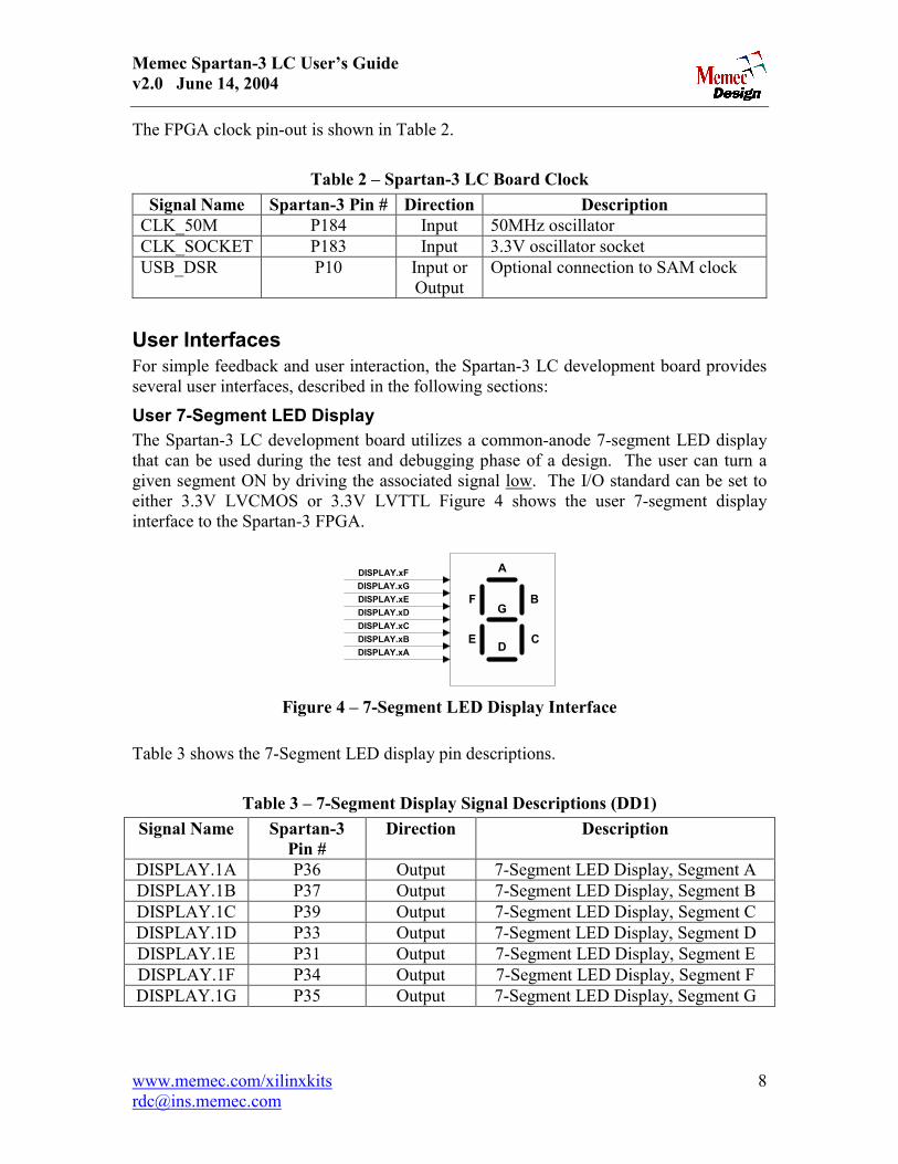
User 7-Segment LED Display The Spartan-3 LC development board utilizes a common-anode 7-segment LED display that can be used during the test and debugging phase of a design. The user can turn a given segment ON by driving the associated signal low. The I/O standard can be set to either 3.3V LVCMOS or 3.3V LVTTL Figure 4 shows the user 7-segment display interface to the Spartan-3 FPGA.
A
B
CDE
FG
DISPLAY.xFDISPLAY.xGDISPLAY.xEDISPLAY.xDDISPLAY.xCDISPLAY.xBDISPLAY.xA
Figure 4 � 7-Segment LED Display Interface
Table 3 shows the 7-Segment LED display pin descriptions.
Table 3 � 7-Segment Display Signal Descriptions (DD1) Signal Name Spartan-3
Pin # Direction Description
DISPLAY.1A P36 Output 7-Segment LED Display, Segment A DISPLAY.1B P37 Output 7-Segment LED Display, Segment B DISPLAY.1C P39 Output 7-Segment LED Display, Segment C DISPLAY.1D P33 Output 7-Segment LED Display, Segment D DISPLAY.1E P31 Output 7-Segment LED Display, Segment E DISPLAY.1F P34 Output 7-Segment LED Display, Segment F DISPLAY.1G P35 Output 7-Segment LED Display, Segment G
Memec Spartan-3 LC User�s Guide v2.0 June 14, 2004
www.memec.com/xilinxkits 9 [email protected]
User LED The Spartan-3 LC development board provides four user LEDs, as shown in Table 4. The I/O standard is 3.3V LVCMOS or 3.3V LVTTL.
Table 4 � User LED Signal Descriptions (DS3, DS4, DS7, DS8) Signal Name Spartan-3
Pin # Direction Description
LED1 P20 Output LED is ON when signal is low LED2 P21 Output LED is ON when signal is low LED3 P18 Output LED is ON when signal is low LED4 P19 Output LED is ON when signal is low
User Push Buttons The Spartan-3 LC development board design provides two user push button switch inputs to the Spartan-3 FPGA. Each push button switch can be used to generate an active low signal. Either push button can be designated to be a RESET signal into the FPGA. Pushing the push button connects the node to Ground (logic low). Internal Spartan-3 pull-ups must be used to force a logic high when the push button is not pushed. A pinout and description of the two push buttons are shown in Table 5.
Table 5 � User Push Button Signal Descriptions (SW4 and SW5) Signal Name Spartan-3
Pin # Direction Description
PUSH1 P22 Input User Push Button Switch Input 1 (SW4) PUSH2 P24 Input User Push Button Switch Input 2 (SW5)
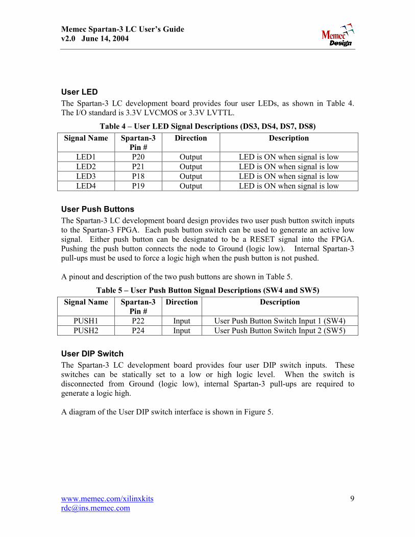
User DIP Switch The Spartan-3 LC development board provides four user DIP switch inputs. These switches can be statically set to a low or high logic level. When the switch is disconnected from Ground (logic low), internal Spartan-3 pull-ups are required to generate a logic high. A diagram of the User DIP switch interface is shown in Figure 5.
Memec Spartan-3 LC User�s Guide v2.0 June 14, 2004
www.memec.com/xilinxkits 10 [email protected]
4321
5678
SW3Switch
DIP4DIP3DIP2DIP1
Figure 5 � User DIP Switch Interface
A pinout and description are shown in Table 6.
Table 6 � User DIP Switch Signal Descriptions (SW3) Signal Name Spartan-3
Pin # Direction Description
DIP1 P26 Input User Switch Input 1 DIP2 P27 Input User Switch Input 2 DIP3 P28 Input User Switch Input 3 DIP4 P29 Input User Switch Input 4
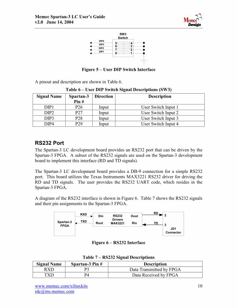
RS232 Port The Spartan-3 LC development board provides an RS232 port that can be driven by the Spartan-3 FPGA. A subset of the RS232 signals are used on the Spartan-3 development board to implement this interface (RD and TD signals). The Spartan-3 LC development board provides a DB-9 connection for a simple RS232 port. This board utilizes the Texas Instruments MAX3221 RS232 driver for driving the RD and TD signals. The user provides the RS232 UART code, which resides in the Spartan-3 FPGA. A diagram of the RS232 interface is shown in Figure 6. Table 7 shows the RS232 signals and their pin assignments to the Spartan-3 FPGA.
RS232Drivers
MAX3221
JD1Connector
RD
TD
2
3Rout
Din
Rin
DoutRXD
TXDSpartan-3FPGA
Figure 6 � RS232 Interface
Table 7 � RS232 Signal Descriptions Signal Name Spartan-3 Pin # Description
RXD P3 Data Transmitted by FPGA TXD P4 Data Received by FPGA
Memec Spartan-3 LC User�s Guide v2.0 June 14, 2004
www.memec.com/xilinxkits 11 [email protected]
USB Port The Spartan-3 LC development board implements a USB 2.0 port. This is accomplished using the Cygnal CP2101 USB-to-UART Bridge Controller. The FPGA interfaces to the CP2101 as a simple UART. The UART interface to the CP2101 can run at speeds ranging from 300 to 921,600 baud. The CP2101 is a highly-integrated USB-to-UART Bridge Controller, providing a simple solution for USB serial communications using a minimum of components and PCB space. The CP2101 includes a USB 2.0 full-speed function controller, USB transceiver, oscillator, EEPROM, and asynchronous serial data bus (UART) with full modem control signals in a compact 5mm X 5mm MLP-28 package. No other external USB components are required. The on-chip EEPROM may be used to customize the USB Vendor ID, Product ID, Product Description String, Power Descriptor, Device Release Number, and Device Serial Number as desired. The EEPROM is programmed on-board via the USB allowing the programming step to be easily integrated into the product manufacturing and testing process. Royalty-free Virtual COM Port (VCP) device drivers provided by Cygnal allow the Spartan-3 LC development board to appear as a COM port to PC applications. The CP2101 UART interface implements all RS232 signals, including control and handshaking signals. These signals are interfaced to the Spartan-3 FPGA as follows:
Table 8 � USB UART Signal Descriptions Signal Name Spartan-3 Pin # Description USB_DTR P9 Data Terminal Ready control output (active low) USB_RTS P13 Ready to Send control output (active low)
USB_SOUT P11 Asynchronous data output (UART Transmit) USB_SIN P12 Asynchronous data input (UART Receive) USB_RI P5 Ring Indicator control input (active low)
USB_DCD P7 Data Carrier Detect control input (active low) USB_DSR P10 Data Set Ready control output (active low) USB_CTS P15 Clear To Send control input (active low)
USB_RESETn P16 CP2101 Device Reset. Open-drain output of internal POR or VDD monitor. An external source can initiate a system reset by driving this pin low
for at least 15 µs
Memec Spartan-3 LC User�s Guide v2.0 June 14, 2004
www.memec.com/xilinxkits 12 [email protected]
Driver Installation To use the USB port, the CP2101 device drivers must be installed. These drivers are included on the Spartan-3 LC Development Kit CD, contained in the self-extracting file CP2101.exe. To install the CP2101 virtual COM port device drivers, do the following:
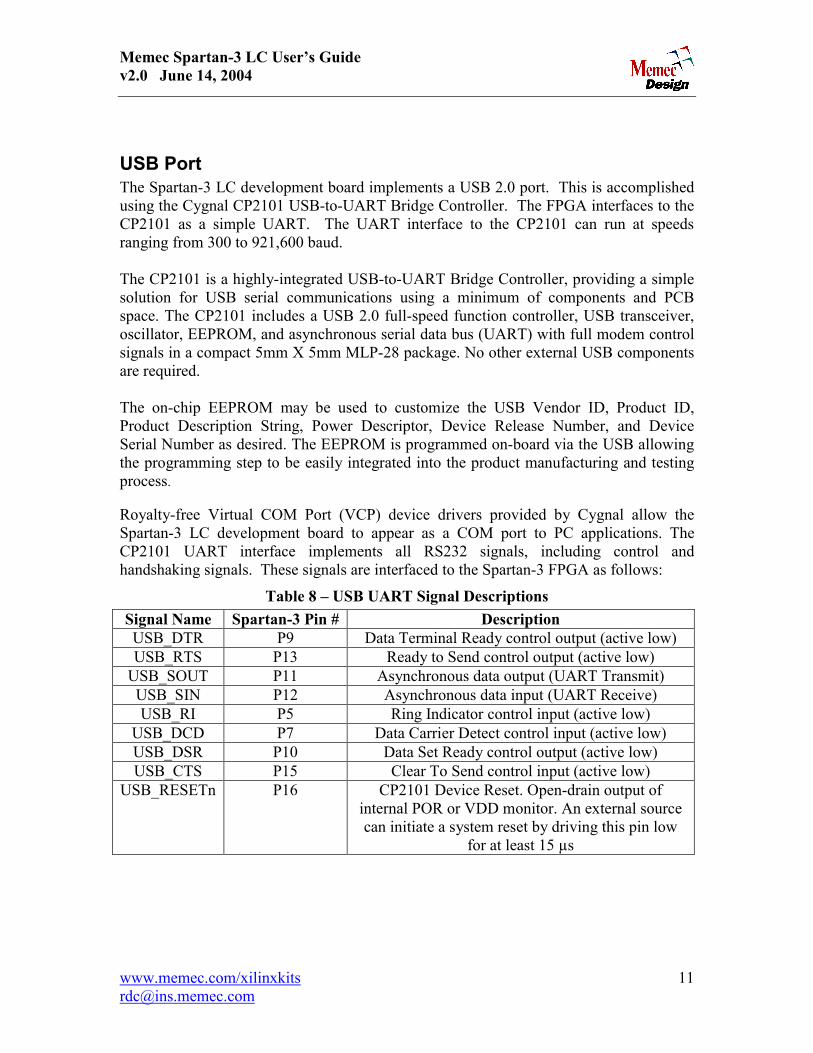
1. Double-click CP2101_Drivers.exe. The InstallShield Wizard to extract the driver installation files launches, as shown in Figure 7. Click Next.
Figure 7 � Launching CP2101 Driver Installation
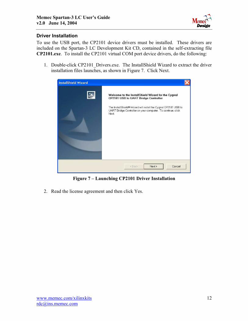
2. Read the license agreement and then click Yes.
Memec Spartan-3 LC User�s Guide v2.0 June 14, 2004
www.memec.com/xilinxkits 13 [email protected]
Figure 8 � Cygnal License Agreement
3. Browse to an acceptable installation directory, then click Next.
Figure 9 � CP2101 Destination Location
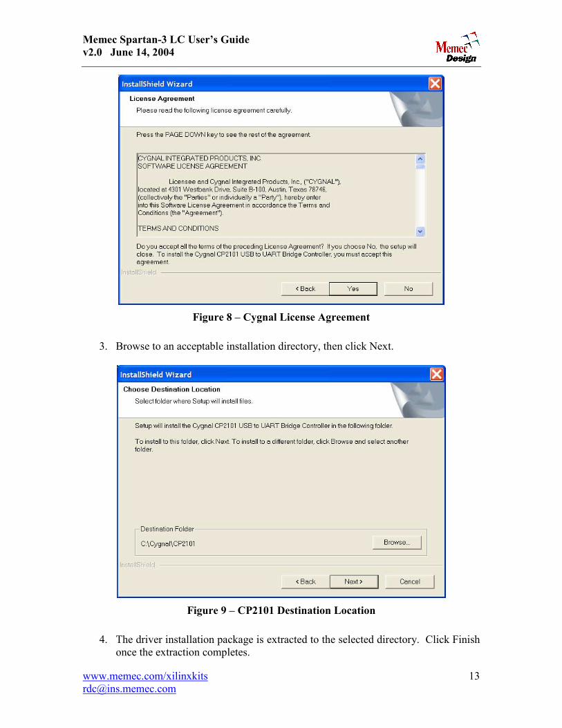
4. The driver installation package is extracted to the selected directory. Click Finish once the extraction completes.
Memec Spartan-3 LC User�s Guide v2.0 June 14, 2004
www.memec.com/xilinxkits 14 [email protected]
Figure 10 � CP2101 Installation Successful
5. To finish the installation, install jumper JP32 and remove all J1 jumpers on a Spartan-3 LC board. Disconnect the 5V power supply.
6. Plug-in a USB cable from the PC to the Spartan-3 LC board. Turn the power switch SW1 to the OFF position. LED DS9 (USB POWER) should now be lit.
7. The Found New Hardware Wizard launches. Click the Install the software automatically (Recommended) radio button (see Figure 11) and then click Next.
Memec Spartan-3 LC User�s Guide v2.0 June 14, 2004
www.memec.com/xilinxkits 15 [email protected]
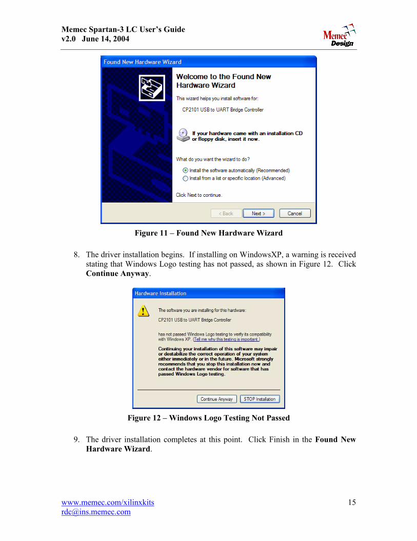
Figure 11 � Found New Hardware Wizard
8. The driver installation begins. If installing on WindowsXP, a warning is received stating that Windows Logo testing has not passed, as shown in Figure 12. Click Continue Anyway.
Figure 12 � Windows Logo Testing Not Passed
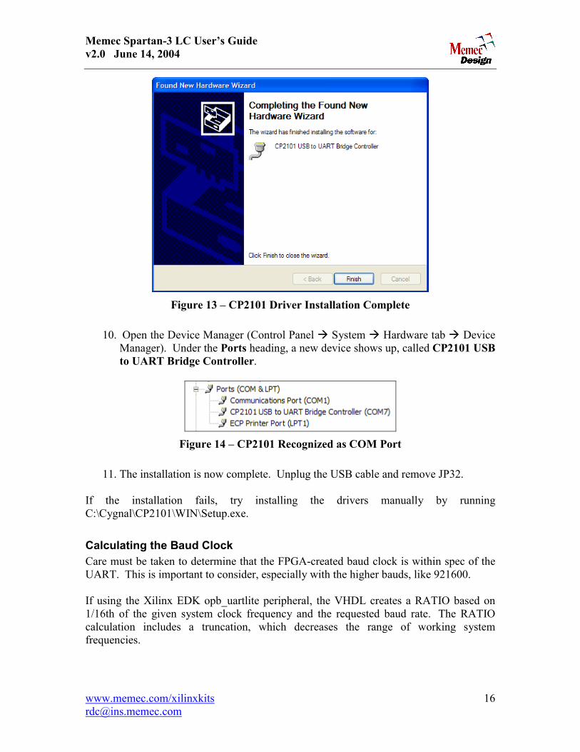
9. The driver installation completes at this point. Click Finish in the Found New Hardware Wizard.
Memec Spartan-3 LC User�s Guide v2.0 June 14, 2004
www.memec.com/xilinxkits 16 [email protected]
Figure 13 � CP2101 Driver Installation Complete
10. Open the Device Manager (Control Panel ! System ! Hardware tab ! Device Manager). Under the Ports heading, a new device shows up, called CP2101 USB to UART Bridge Controller.
Figure 14 � CP2101 Recognized as COM Port
11. The installation is now complete. Unplug the USB cable and remove JP32. If the installation fails, try installing the drivers manually by running C:\Cygnal\CP2101\WIN\Setup.exe.
Calculating the Baud Clock Care must be taken to determine that the FPGA-created baud clock is within spec of the UART. This is important to consider, especially with the higher bauds, like 921600. If using the Xilinx EDK opb_uartlite peripheral, the VHDL creates a RATIO based on 1/16th of the given system clock frequency and the requested baud rate. The RATIO calculation includes a truncation, which decreases the range of working system frequencies.
Memec Spartan-3 LC User�s Guide v2.0 June 14, 2004
www.memec.com/xilinxkits 17 [email protected]
Based on this RATIO, the actual baud rate is created. It is recommended that the actual baud rate be within 2% of the requested baud in order for the serial communication to work. With a 2% allowed error, the equations to use for opb_uartlite are: RATIO = Truncate(C_CLK_FREQ / (16 * Requested_C_BAUDRATE)) Actual_C_BAUDRATE = C_CLK_FREQ / (16 * RATIO) Error = 1 - (Requested/Actual) <= 2% As an example, consider creating a 19200 BAUD UART from a 100 MHz system clock: RATIO = Truncate(100M / (16 * 19200)) = 325 Actual_C_BAUDRATE = 100 M / (16 * 325) = 19230.77 Error = 1 - (19200/19230.77) = 0.16% Since this is much less than 2%, this clock configuration works cleanly with the UART. However, consider what happens with higher bauds: To generate 921600 from a 66.666667 MHz clock, the calculations show: Ratio = 4 Actual_C_BAUDRATE = 1,041,667 Error = 13% Interestingly, a 50 MHz system clock achieves: Ratio = 3 Actual_C_BAUDRATE = 1,041,667 Error = 13% In both of these cases, the 3SLC board USB UART will output garbled communications on the HyperTerminal. However, if 60 MHz is the system clock, the calculations show: Ratio = 4 Actual_C_BAUDRATE = 937,500 Error = 1.7% 75 MHz is likewise acceptable: Ratio = 5 Actual_C_BAUDRATE = 937,500 Error = 1.7% Both of these cases work on the 3SLC USB UART. A spreadsheet (uartlite_clock_ratios.xls) is available on the Memec Reference Design Center that charts the calculations for the higher baud rates. The resulting values identify acceptable system clock frequencies for generating the higher baud rates.
Memec Spartan-3 LC User�s Guide v2.0 June 14, 2004
www.memec.com/xilinxkits 18 [email protected]
Configuration Support The Spartan-3 LC development board supports three different FPGA configuration methods, which are described below.
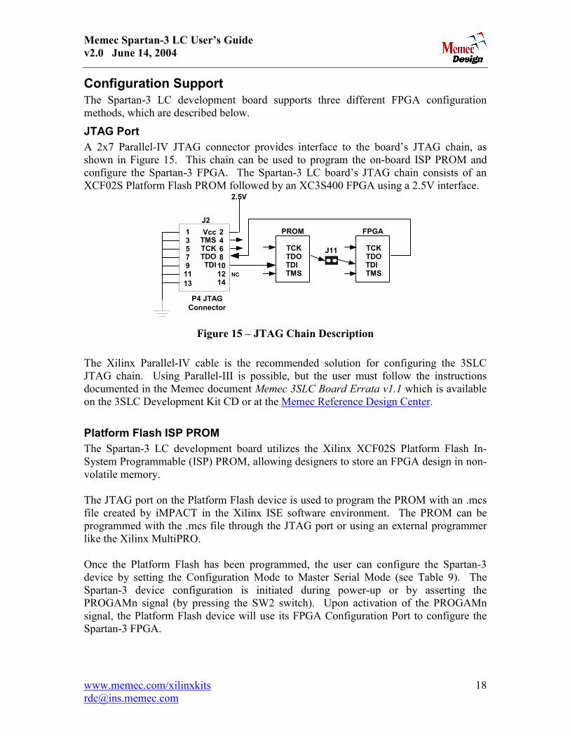
JTAG Port A 2x7 Parallel-IV JTAG connector provides interface to the board�s JTAG chain, as shown in Figure 15. This chain can be used to program the on-board ISP PROM and configure the Spartan-3 FPGA. The Spartan-3 LC board�s JTAG chain consists of an XCF02S Platform Flash PROM followed by an XC3S400 FPGA using a 2.5V interface.
P4 JTAGConnector
TCKTDOTDITMS
PROM
TCKTDOTDITMS
FPGA
J11TMS
1 246
7
35
89 10
1214
1113
2.5V
TCKTDOTDI
VccJ2
NC
Figure 15 � JTAG Chain Description
The Xilinx Parallel-IV cable is the recommended solution for configuring the 3SLC JTAG chain. Using Parallel-III is possible, but the user must follow the instructions documented in the Memec document Memec 3SLC Board Errata v1.1 which is available on the 3SLC Development Kit CD or at the Memec Reference Design Center.
Platform Flash ISP PROM The Spartan-3 LC development board utilizes the Xilinx XCF02S Platform Flash In-System Programmable (ISP) PROM, allowing designers to store an FPGA design in non-volatile memory. The JTAG port on the Platform Flash device is used to program the PROM with an .mcs file created by iMPACT in the Xilinx ISE software environment. The PROM can be programmed with the .mcs file through the JTAG port or using an external programmer like the Xilinx MultiPRO. Once the Platform Flash has been programmed, the user can configure the Spartan-3 device by setting the Configuration Mode to Master Serial Mode (see Table 9). The Spartan-3 device configuration is initiated during power-up or by asserting the PROGAMn signal (by pressing the SW2 switch). Upon activation of the PROGAMn signal, the Platform Flash device will use its FPGA Configuration Port to configure the Spartan-3 FPGA.
Memec Spartan-3 LC User�s Guide v2.0 June 14, 2004
www.memec.com/xilinxkits 19 [email protected]
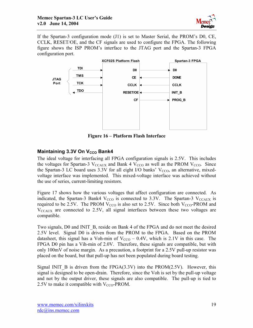
If the Spartan-3 configuration mode (J1) is set to Master Serial, the PROM�s D0, CE, CCLK, RESET/OE, and the CF signals are used to configure the FPGA. The following figure shows the ISP PROM�s interface to the JTAG port and the Spartan-3 FPGA configuration port.
JTAGPort CCLK
DONE
INIT_B
PROG_B
D0
CF
CE
RESET/OE
CCLK
D0
Spartan-3 FPGAXCF02S Platform Flash
TDI
TMS
TCK
TDO
Figure 16 � Platform Flash Interface
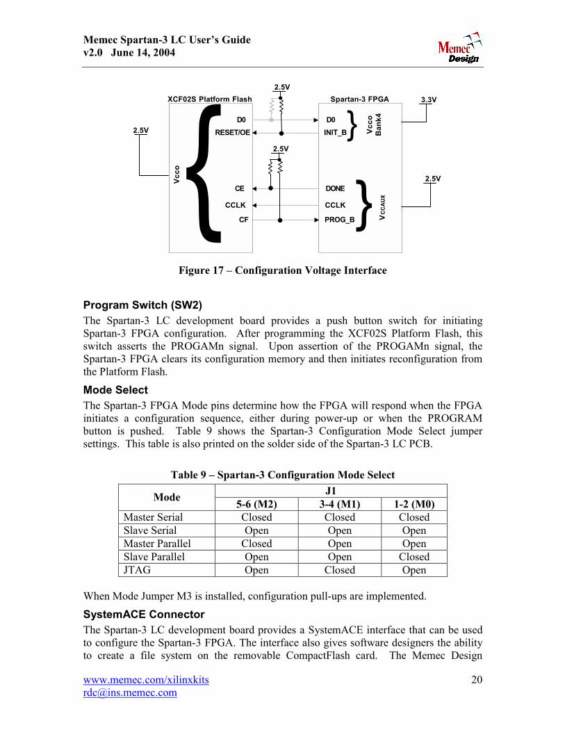
Maintaining 3.3V On VCCO Bank4 The ideal voltage for interfacing all FPGA configuration signals is 2.5V. This includes the voltages for Spartan-3 VCCAUX and Bank 4 VCCO as well as the PROM VCCO. Since the Spartan-3 LC board uses 3.3V for all eight I/O banks� VCCO, an alternative, mixed-voltage interface was implemented. This mixed-voltage interface was achieved without the use of series, current-limiting resistors. Figure 17 shows how the various voltages that affect configuration are connected. As indicated, the Spartan-3 Bank4 VCCO is connected to 3.3V. The Spartan-3 VCCAUX is required to be 2.5V. The PROM VCCO is also set to 2.5V. Since both VCCO-PROM and VCCAUX are connected to 2.5V, all signal interfaces between these two voltages are compatible. Two signals, D0 and INIT_B, reside on Bank 4 of the FPGA and do not meet the desired 2.5V level. Signal D0 is driven from the PROM to the FPGA. Based on the PROM datasheet, this signal has a Voh-min of VCCO � 0.4V, which is 2.1V in this case. The FPGA D0 pin has a Vih-min of 2.0V. Therefore, these signals are compatible, but with only 100mV of noise margin. As a precaution, a footprint for a 2.5V pull-up resistor was placed on the board, but that pull-up has not been populated during board testing. Signal INIT_B is driven from the FPGA(3.3V) into the PROM(2.5V). However, this signal is designed to be open-drain. Therefore, since the Voh is set by the pull-up voltage and not by the output driver, these signals are also compatible. The pull-up is tied to 2.5V to make it compatible with VCCO-PROM.
Memec Spartan-3 LC User�s Guide v2.0 June 14, 2004
www.memec.com/xilinxkits 20 [email protected]
CCLK
DONE
INIT_B
PROG_B
D0
CF
CE
RESET/OE
CCLK
D0
Spartan-3 FPGAXCF02S Platform Flash
}
}
Vcc
oB
ank4
VC
CA
UX
Vcc
o
2.5V
2.5V
3.3V
{ 2.5V
2.5V
Figure 17 � Configuration Voltage Interface
Program Switch (SW2) The Spartan-3 LC development board provides a push button switch for initiating Spartan-3 FPGA configuration. After programming the XCF02S Platform Flash, this switch asserts the PROGAMn signal. Upon assertion of the PROGAMn signal, the Spartan-3 FPGA clears its configuration memory and then initiates reconfiguration from the Platform Flash.
Mode Select The Spartan-3 FPGA Mode pins determine how the FPGA will respond when the FPGA initiates a configuration sequence, either during power-up or when the PROGRAM button is pushed. Table 9 shows the Spartan-3 Configuration Mode Select jumper settings. This table is also printed on the solder side of the Spartan-3 LC PCB.
Table 9 � Spartan-3 Configuration Mode Select J1 Mode 5-6 (M2) 3-4 (M1) 1-2 (M0)
Master Serial Closed Closed Closed Slave Serial Open Open Open Master Parallel Closed Open Open Slave Parallel Open Open Closed JTAG Open Closed Open
When Mode Jumper M3 is installed, configuration pull-ups are implemented.
SystemACE Connector The Spartan-3 LC development board provides a SystemACE interface that can be used to configure the Spartan-3 FPGA. The interface also gives software designers the ability to create a file system on the removable CompactFlash card. The Memec Design
Memec Spartan-3 LC User�s Guide v2.0 June 14, 2004
www.memec.com/xilinxkits 21 [email protected]
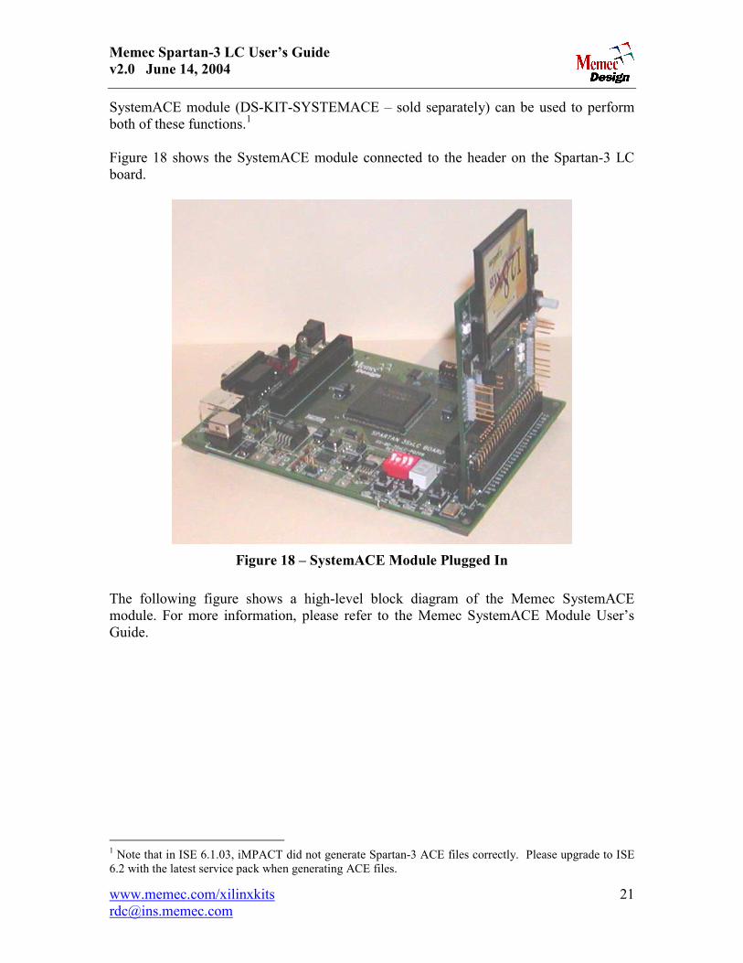
SystemACE module (DS-KIT-SYSTEMACE � sold separately) can be used to perform both of these functions.1 Figure 18 shows the SystemACE module connected to the header on the Spartan-3 LC board.
Figure 18 � SystemACE Module Plugged In
The following figure shows a high-level block diagram of the Memec SystemACE module. For more information, please refer to the Memec SystemACE Module User�s Guide.
1 Note that in ISE 6.1.03, iMPACT did not generate Spartan-3 ACE files correctly. Please upgrade to ISE 6.2 with the latest service pack when generating ACE files.

Memec Spartan-3 LC User�s Guide v2.0 June 14, 2004
www.memec.com/xilinxkits 22 [email protected]
50-pin Connector(connects to a 50-pin 0.1" square post header on the main board)
SystemACE�Controller
284
JTAGConfiguration Port
MPUInterface
Power &Ground
10 8
MiscSignals
CompactFlahConnector
JTA
GTe
st P
ort
JTA
GC
onfig
urat
ion
Port
CompactFlahInterface
MPUInterface
JTA
GC
onne
ctor
JTA
GC
onne
ctor
OSC@25 MHz
ResetSwitch
Para
llel C
able
IVC
onne
ctor
Figure 19 � SystemACE Module Block Diagram
When the MPU port of the SystemACE controller is used, the FPGA and the SystemACE controller must use the same clock source. Hence, a jumper is provided on the Spartan-3 LC development board and the SystemACE module to provide the clock input to both devices. The following table shows the required jumper connections.
Memec Spartan-3 LC User�s Guide v2.0 June 14, 2004
www.memec.com/xilinxkits 23 [email protected]
Table 10 � SystemACE Controller Clock Source
Jumper Settings Clock Source JP30 (3SLC board) JP5 (SAM board)
SystemACE module 25Mhz OSC Close
Open (25MHz osc enabled)
FPGA-generated clock < 33 MHz output on P10
Close Close
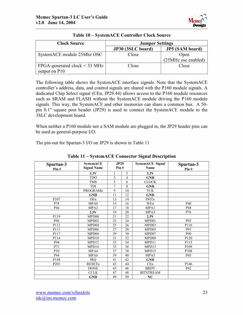
The following table shows the SystemACE interface signals. Note that the SystemACE controller�s address, data, and control signals are shared with the P160 module signals. A dedicated Chip Select signal (CEn, JP29.44) allows access to the P160 module resources such as SRAM and FLASH without the SystemACE module driving the P160 module signals. This way, the SystemACE and other memories can share a common bus. A 50-pin 0.1� square post header (JP29) is used to connect the SystemACE module to the 3SLC development board. When neither a P160 module nor a SAM module are plugged in, the JP29 header pins can be used as general-purpose I/O. The pin-out for Spartan-3 I/O on JP29 is shown in Table 11
Table 11 � SystemACE Connector Signal Description
Spartan-3 Pin #
SystemACE Signal Name
JP29 Pin #
SystemACE Signal Name
Spartan-3 Pin #
3.3V 1 2 3.3V TDO 3 4 GND TMS 5 6 CLOCK TDI 7 8 GND PROGRAMn 9 10 TCK GND 11 12 GND
P107 OEn 13 14 INITn P78 MPA0 15 16 WEn P40 P46 MPA2 17 18 MPA1 P48
2.5V 19 20 MPA3 P76 P119 MPD00 21 22 2.5V P96 MPD02 23 24 MPD01 P95
P113 MPD04 25 26 MPD03 P116 P111 MPD06 27 28 MPD05 P93 P117 MPD08 29 30 MPD07 P90 P114 MPD10 31 32 MPD09 P120 P94 MPD12 33 34 MPD11 P115 P71 MPD14 35 36 MPD13 P109 P50 MPA4 37 38 MPD15 P108 P44 MPA6 39 40 MPA5 P45
P148 IRQ 41 42 GND P203 RESETn 43 44 CEn P146
DONE 45 46 BRDY P42 CCLK 47 48 BITSTREAM GND 49 50 NC
Memec Spartan-3 LC User�s Guide v2.0 June 14, 2004
www.memec.com/xilinxkits 24 [email protected]
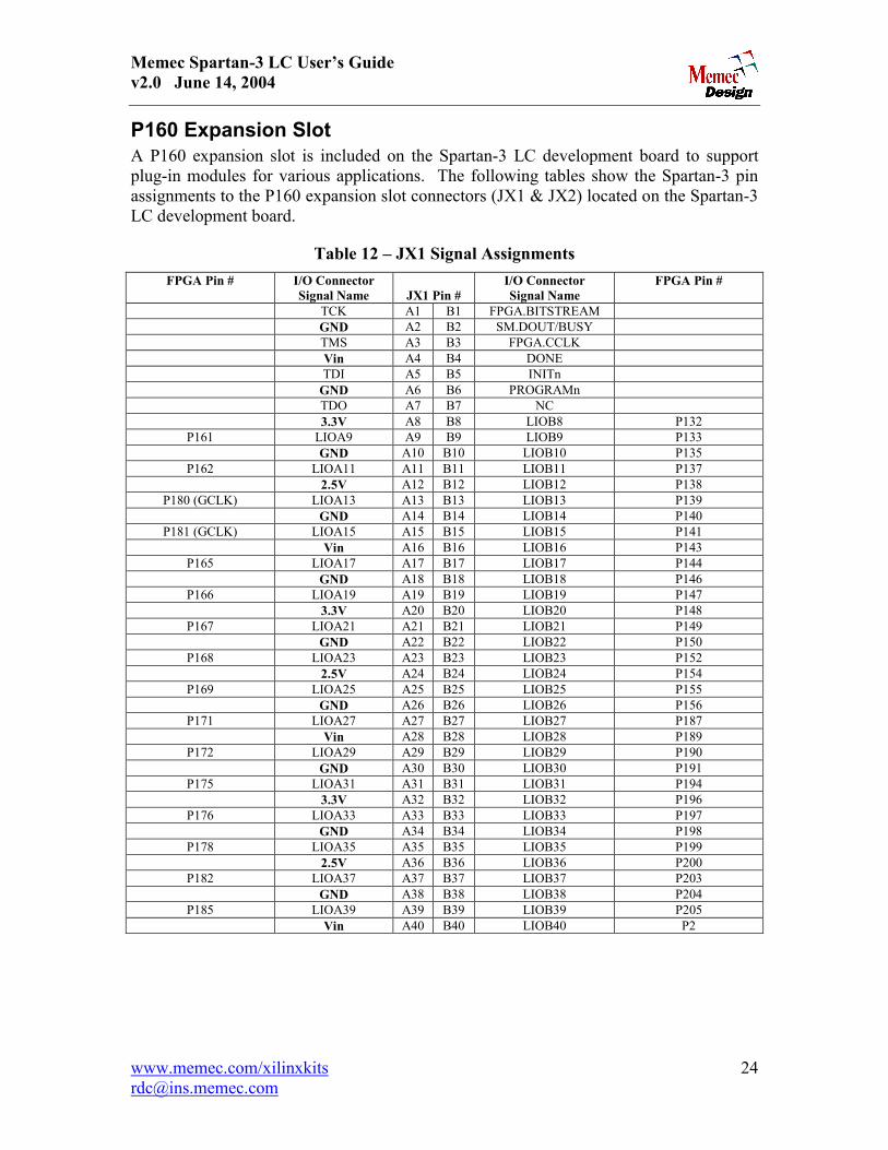
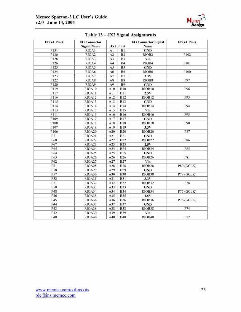
P160 Expansion Slot A P160 expansion slot is included on the Spartan-3 LC development board to support plug-in modules for various applications. The following tables show the Spartan-3 pin assignments to the P160 expansion slot connectors (JX1 & JX2) located on the Spartan-3 LC development board.
Table 12 � JX1 Signal Assignments FPGA Pin # I/O Connector
Signal Name
JX1 Pin # I/O Connector Signal Name
FPGA Pin #
TCK A1 B1 FPGA.BITSTREAM GND A2 B2 SM.DOUT/BUSY TMS A3 B3 FPGA.CCLK Vin A4 B4 DONE TDI A5 B5 INITn GND A6 B6 PROGRAMn TDO A7 B7 NC 3.3V A8 B8 LIOB8 P132
P161 LIOA9 A9 B9 LIOB9 P133 GND A10 B10 LIOB10 P135
P162 LIOA11 A11 B11 LIOB11 P137 2.5V A12 B12 LIOB12 P138
P180 (GCLK) LIOA13 A13 B13 LIOB13 P139 GND A14 B14 LIOB14 P140
P181 (GCLK) LIOA15 A15 B15 LIOB15 P141 Vin A16 B16 LIOB16 P143
P165 LIOA17 A17 B17 LIOB17 P144 GND A18 B18 LIOB18 P146
P166 LIOA19 A19 B19 LIOB19 P147 3.3V A20 B20 LIOB20 P148
P167 LIOA21 A21 B21 LIOB21 P149 GND A22 B22 LIOB22 P150
P168 LIOA23 A23 B23 LIOB23 P152 2.5V A24 B24 LIOB24 P154
P169 LIOA25 A25 B25 LIOB25 P155 GND A26 B26 LIOB26 P156
P171 LIOA27 A27 B27 LIOB27 P187 Vin A28 B28 LIOB28 P189
P172 LIOA29 A29 B29 LIOB29 P190 GND A30 B30 LIOB30 P191
P175 LIOA31 A31 B31 LIOB31 P194 3.3V A32 B32 LIOB32 P196
P176 LIOA33 A33 B33 LIOB33 P197 GND A34 B34 LIOB34 P198
P178 LIOA35 A35 B35 LIOB35 P199 2.5V A36 B36 LIOB36 P200
P182 LIOA37 A37 B37 LIOB37 P203 GND A38 B38 LIOB38 P204
P185 LIOA39 A39 B39 LIOB39 P205 Vin A40 B40 LIOB40 P2
Memec Spartan-3 LC User�s Guide v2.0 June 14, 2004
www.memec.com/xilinxkits 25 [email protected]
Table 13 � JX2 Signal Assignments FPGA Pin # I/O Connector
Signal Name
JX2 Pin # I/O Connector Signal
Name FPGA Pin #
P131 RIOA1 A1 B1 GND P130 RIOA2 A2 B2 RIOB2 P102 P128 RIOA3 A3 B3 Vin P126 RIOA4 A4 B4 RIOB4 P101 P125 RIOA5 A5 B5 GND P124 RIOA6 A6 B6 RIOB6 P100 P123 RIOA7 A7 B7 3.3V P122 RIOA8 A8 B8 RIOB8 P97 P120 RIOA9 A9 B9 GND P119 RIOA10 A10 B10 RIOB10 P96 P117 RIOA11 A11 B11 2.5V P116 RIOA12 A12 B12 RIOB12 P95 P115 RIOA13 A13 B13 GND P114 RIOA14 A14 B14 RIOB14 P94 P113 RIOA15 A15 B15 Vin P111 RIOA16 A16 B16 RIOB16 P93 P109 RIOA17 A17 B17 GND P108 RIOA18 A18 B18 RIOB18 P90 P107 RIOA19 A19 B19 3.3V P106 RIOA20 A20 B20 RIOB20 P87 P71 RIOA21 A21 B21 GND P68 RIOA22 A22 B22 RIOB22 P86 P67 RIOA23 A23 B23 2.5V P65 RIOA24 A24 B24 RIOB24 P85 P64 RIOA25 A25 B25 GND P63 RIOA26 A26 B26 RIOB26 P81 P62 RIOA27 A27 B27 Vin P61 RIOA28 A28 B28 RIOB28 P80 (GCLK) P58 RIOA29 A29 B29 GND P57 RIOA30 A30 B30 RIOB30 P79 (GCLK) P52 RIOA31 A31 B31 3.3V P51 RIOA32 A32 B32 RIOB32 P78 P50 RIOA33 A33 B33 GND P48 RIOA34 A34 B34 RIOB34 P77 (GCLK) P46 RIOA35 A35 B35 2.5V P45 RIOA36 A36 B36 RIOB36 P76 (GCLK) P44 RIOA37 A37 B37 GND P43 RIOA38 A38 B38 RIOB38 P74 P42 RIOA39 A39 B39 Vin P40 RIOA40 A40 B40 RIOB40 P72

Memec Spartan-3 LC User�s Guide v2.0 June 14, 2004
www.memec.com/xilinxkits 26 [email protected]
Power System Design The Spartan-3 LC development board�s power system is designed to meet the required Xilinx power specifications for the Spartan-3 FPGA on all three rails: VCCINT, VCCAUX, and VCCO. These specifications include:
• VNOMINAL +/- 5% • Monotonic ramp on VCCINT, VCCAUX, and VCCO-Bank4 • VCCO Ramp Time > 2ms
Although not required, VCCINT and VCCAUX were designed to allow an adjustable ramp time. This is helpful in controlling the power-on surge current from the bypass capacitors, which in turn helps to achieve a monotonic rise. The Spartan-3 LC development board incorporates a 5V supervisor and staggered power-up to reduce the instantaneous demand on the input power supply. Note that this sequencing is NOT required by the Spartan-3 FPGA (see the Spartan-3 datasheet for more details). Three sources are available for the 5V input supply. The primary source is a 5V/2A AC/DC converter included in the Spartan-3 LC Development Kit. Secondly, the USB port is capable of providing 5V/500mA. To power the board from the USB port, do the following:
• Install JP32 • Slide SW1 to the OFF position • Plug in a USB cable from a PC to the board
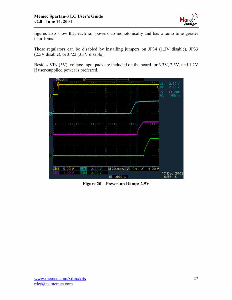
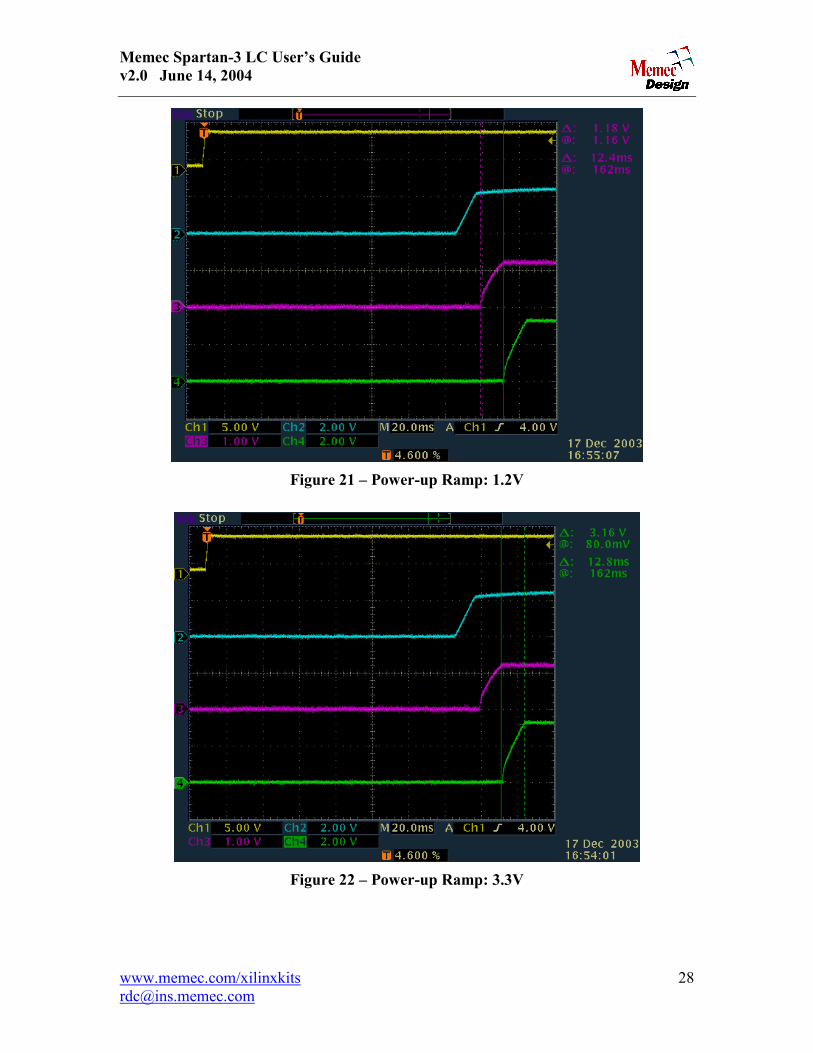
A user-supplied 5V source can also be easily connected to the board through the 5V pad near JP1. As shown in the schematic, 5V is regulated to 1.2V, 2.5V, and 3.3V. The 2.5V and 3.3V circuits use the Texas Instruments� ultra-low noise, low-dropout, linear regulator family. The TPS78633KTT is used to regulate 1.5A at 3.3V. The TPS79525DCQ is used to regulate 500mA at 2.5V. Since these LDOs have an extremely fast power-on ramp, a simple soft-start circuit is incorporated into the design to control the ramp time. The TPS54110PWP, a member of the TI SWIFT� switching converter family, is used to regulate 1.5A at 1.2V. This circuit has built-in soft-start and power-good capabilities. The TI TLC7733 supervisor monitors 5V. Once 5V trips the supervisor�s threshold, a programmable delay timer set to approximately 140ms is triggered. After the delay time, the circuit enables the 2.5V regulator. The 2.5V regulator output in turn enables the 1.2V SWIFT. The PWRGD output of the SWIFT is used to enable the 3.3V LDO. This staggered power-on is displayed in several figures, beginning with Figure 20. These
Memec Spartan-3 LC User�s Guide v2.0 June 14, 2004
www.memec.com/xilinxkits 27 [email protected]
figures also show that each rail powers up monotonically and has a ramp time greater than 10ms. These regulators can be disabled by installing jumpers on JP34 (1.2V disable), JP33 (2.5V disable), or JP22 (3.3V disable). Besides VIN (5V), voltage input pads are included on the board for 3.3V, 2.5V, and 1.2V if user-supplied power is preferred.
Figure 20 � Power-up Ramp: 2.5V
Memec Spartan-3 LC User�s Guide v2.0 June 14, 2004
www.memec.com/xilinxkits 28 [email protected]
Figure 21 � Power-up Ramp: 1.2V
Figure 22 � Power-up Ramp: 3.3V
Memec Spartan-3 LC User�s Guide v2.0 June 14, 2004
www.memec.com/xilinxkits 29 [email protected]
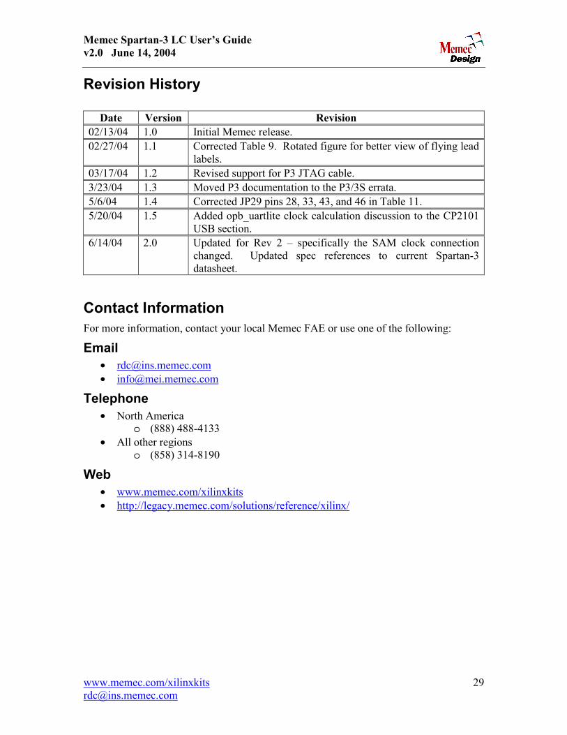
Revision History
Date Version Revision 02/13/04 1.0 Initial Memec release. 02/27/04 1.1 Corrected Table 9. Rotated figure for better view of flying lead
labels. 03/17/04 1.2 Revised support for P3 JTAG cable. 3/23/04 1.3 Moved P3 documentation to the P3/3S errata. 5/6/04 1.4 Corrected JP29 pins 28, 33, 43, and 46 in Table 11. 5/20/04 1.5 Added opb_uartlite clock calculation discussion to the CP2101
USB section. 6/14/04 2.0 Updated for Rev 2 � specifically the SAM clock connection
changed. Updated spec references to current Spartan-3 datasheet.
Contact Information For more information, contact your local Memec FAE or use one of the following:
Email • [email protected] • [email protected]
Telephone • North America
o (888) 488-4133 • All other regions
o (858) 314-8190
Web • www.memec.com/xilinxkits • http://legacy.memec.com/solutions/reference/xilinx/