Embed Size (px)
Citation preview
73
Orii et al.: Micro Structure Observation and Reliability Behavior (1/14)
[Technical Paper]
Micro Structure Observation and Reliability Behavior of Peripheral
Flip Chip Interconnections with Solder-Capped Cu Pillar BumpsYasumitsu Orii*, Kazushige Toriyama*, Sayuri Kohara*, Hirokazu Noma*, Keishi Okamoto*, Daisuke Toyoshima**,
and Keisuke Uenishi**
*IBM Research Tokyo, 1623-14, Shimotsuruma, Yamato-city, Kanagawa-ken 242-8502, Japan
**Osaka University, 2-1, Yamadaoka, Suita, Osaka 565-0871, Japan
(Received September 1, 2011; accepted November 10, 2011)
Abstract
PoP (Package on Package) structures have been used widely in digital consumer electronics products such as digital still
cameras and mobile phones. However, the final stack height from the top to the bottom package for these structures is
higher than that of the current stacked die packages. To reduce the height of the package, a flip chip technology is used.
Since the logic chips of mobile applications use a pad pitch of less than 80 μm or less, an ultra-fine-pitch flip chip intercon-
nection technique is required. The C4 (Controlled Collapse Chip Connection) flip chip technology is widely used in area
array flip chip packages. The C4 was named after the four initial characters which are “C” of Controlled Collapse Chip
Connection. The collapse of the molten solder is controlled by the individual opening of solder resist on each pad on the
substrate so that the chip can be connected onto the substrate. However, C4 is not suitable in the ultra-fine-pitch flip chips
because the such a individual opening which is suitable for the ultra-fine-pitch cannot be made on the substraete. Instead
of the C4 flip chip technology, the new interconnection technique was developed using the solder capped Cu pillar bumps.
It is very easy to control the space between the die and the substrate by adjusting the Cu pillar height even when a large
slit window opening exists on a group of pads on the substrate. Since the collapse control of the solder bumps is not
necessary, we call the process C2 (Chip Connection). The C2 was named after the two initial characters which are “C”
of Chip Connection. The solder capped Cu pillar bumps are connected to Cu substrate pads, which are a surface treated
with OSP (Organic Solder Preservative), by reflow with no-clean processes. This technology creates the SMT (Surface
Mount Technology)/flip chip hybrid assembly for SoP (System on Package) use. We have produced 50 μm pitch intercon-
nections and observed the micro structure and tested their reliability. Some voids in the solder joint were observed after
the reflow process. The results of warpage measurements and FEM (Finite Element Method) analyses suggest that these
voids are the shrinkage voids caused by the wide temperature range of the solder liquid phase and the substrate warpage.
Since they are not the stress induced voids, they didn’t affect the reliability test. The increase in interconnection resis-
tance during the reliability test was compared between the C2 interconnection and Au stud-solder interconnection. Since
the resistance increase of the C2 interconnection is much smaller than that for the Au stud-solder interconnection, it is
clear that the C2 flip chip technology provides robust solder connections at low cost. Also the C2 structure with a low-k
device was evaluated and no failures were observed at 1,500 cycles in the TC (Thermal Cycle) test. In addition to the
fine-pitch interconnections, a die thickness of 70 μm is required to reduce the final stack height. The reliability perfor-
mance of the C2 flip chip with the die thicknesses 20 μm, 70 μm and 150 μm was also discussed using a PEG (Post-
Encapsulation Grinding) method in which the die is ground to less than 70 μm after joining and underfilling. Finally the
electromigration tests were performed on the 80 μm pitch C2 interconnection. The tests showed that the solder capped
Cu pillar structure has high endurance against electromigration and no failure data was recorded up to 1,000 hrs with
several electromigration conditions regardless the direction of electron flow.
Keywords: Flip Chip, Cu Pillar, Shrinkage, Thin Die, Electromigration, Low-k, IMC
74
Transactions of The Japan Institute of Electronics Packaging Vol. 4, No. 1, 2011
1. IntroductionPoP[1] is an emerging technology intended to replace
the wire-bonding stacked die technology.[2] It has been
widely used in digital consumer electronics products such
as digital still cameras and mobile phones. One of the dis-
advantages of PoP is that the final stack-up-height, from
the top to the bottom of the package, is greater than that
for the stacked die packages. For this reason, Flip-Chip-
PoP, in which the flip chip technology is used for the bot-
tom package, became popular. Since the die of the bottom
packages in PoP is designed for the wire-bonding technol-
ogy, the I/O pads are located on the periphery of the die
with a fine-pitch, such as 80 μm or less. A number of flip
chip interconnection methods are available in the industry,
but only few technologies are dedicated for ultra-fine-pitch
flip chips on organic substrates. The technology widely
used in Japan for digital still cameras and mobile phones is
Au stud-solder interconnections.[3] However, this technol-
ogy is high-cost, low-throughput and not SMT compatible.
There are three known drawbacks for this technology.
One of the drawbacks being the need for the pre-formed
Sn-Ag solder on the Cu pads of the substrates. This
increases the manufacturing costs and results in a large
variation in solder heights, since the solder heights are
determined by the Cu pad widths. The technology has a
long processing time due to the thermal compression
bonding performed for each die. The bonding also
requires an expensive equipment. The other drawback is
the narrow process margin due to the creation of compli-
cated IMC (Intermetallic Compounds) which increases
the interconnection resistance. These drawbacks inhibit
the expanded use of the flip chip infrastructures. A new
technology is needed to extend the standard C4 technol-
ogy that was introduced by IBM in the early 1960s for its
SLC (Solid Logic Technology). The C4 technology is a
high-throughput flip chip technology and is still widely
used for CPUs in PCs and games. However, this technol-
ogy is normally used for the systems having bump pitch of
greater than 150 μm and is not suited for the fine-pitch
applications. In the fine-pitch systems, the space between
the die and the substrate becomes narrow which can
cause solder bridges in the C4 technology because of the
collapsing of the bumps. The underfill insertion is also dif-
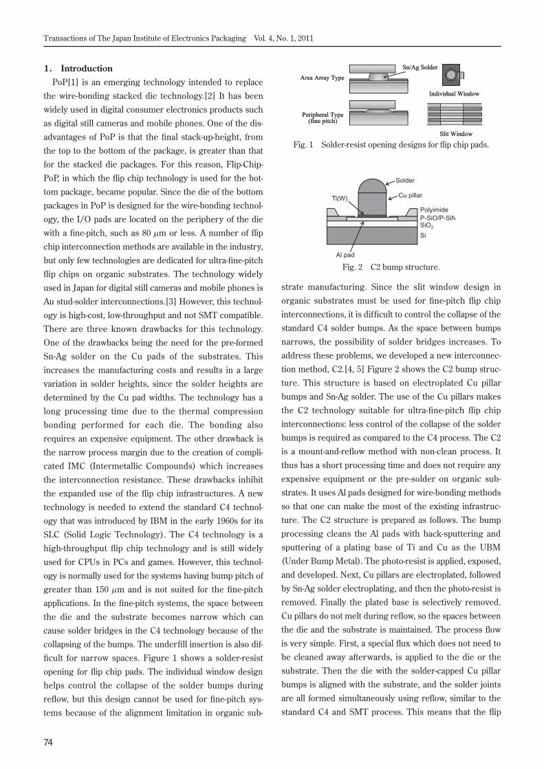
ficult for narrow spaces. Figure 1 shows a solder-resist
opening for flip chip pads. The individual window design
helps control the collapse of the solder bumps during
reflow, but this design cannot be used for fine-pitch sys-
tems because of the alignment limitation in organic sub-
strate manufacturing. Since the slit window design in
organic substrates must be used for fine-pitch flip chip
interconnections, it is difficult to control the collapse of the
standard C4 solder bumps. As the space between bumps
narrows, the possibility of solder bridges increases. To
address these problems, we developed a new interconnec-
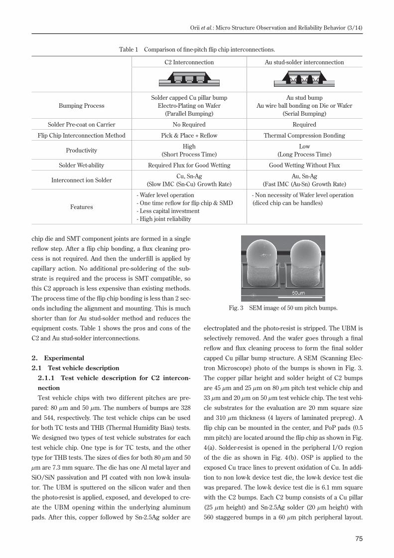
tion method, C2.[4, 5] Figure 2 shows the C2 bump struc-
ture. This structure is based on electroplated Cu pillar
bumps and Sn-Ag solder. The use of the Cu pillars makes
the C2 technology suitable for ultra-fine-pitch flip chip
interconnections: less control of the collapse of the solder
bumps is required as compared to the C4 process. The C2
is a mount-and-reflow method with non-clean process. It
thus has a short processing time and does not require any
expensive equipment or the pre-solder on organic sub-
strates. It uses Al pads designed for wire-bonding methods
so that one can make the most of the existing infrastruc-
ture. The C2 structure is prepared as follows. The bump
processing cleans the Al pads with back-sputtering and
sputtering of a plating base of Ti and Cu as the UBM
(Under Bump Metal). The photo-resist is applied, exposed,
and developed. Next, Cu pillars are electroplated, followed
by Sn-Ag solder electroplating, and then the photo-resist is
removed. Finally the plated base is selectively removed.
Cu pillars do not melt during reflow, so the spaces between
the die and the substrate is maintained. The process flow
is very simple. First, a special flux which does not need to
be cleaned away afterwards, is applied to the die or the
substrate. Then the die with the solder-capped Cu pillar
bumps is aligned with the substrate, and the solder joints
are all formed simultaneously using reflow, similar to the
standard C4 and SMT process. This means that the flip
Fig. 2 C2 bump structure.
Fig. 1 Solder-resist opening designs for flip chip pads.
75
Orii et al.: Micro Structure Observation and Reliability Behavior (3/14)
chip die and SMT component joints are formed in a single
reflow step. After a flip chip bonding, a flux cleaning pro-
cess is not required. And then the underfill is applied by
capillary action. No additional pre-soldering of the sub-
strate is required and the process is SMT compatible, so
this C2 approach is less expensive than existing methods.
The process time of the flip chip bonding is less than 2 sec-
onds including the alignment and mounting. This is much
shorter than for Au stud-solder method and reduces the
equipment costs. Table 1 shows the pros and cons of the
C2 and Au stud-solder interconnections.
2. Experimental2.1 Test vehicle description
2.1.1 Test vehicle description for C2 intercon-nectionTest vehicle chips with two different pitches are pre-
pared: 80 μm and 50 μm. The numbers of bumps are 328
and 544, respectively. The test vehicle chips can be used
for both TC tests and THB (Thermal Humidity Bias) tests.
We designed two types of test vehicle substrates for each
test vehicle chip. One type is for TC tests, and the other
type for THB tests. The sizes of dies for both 80 μm and 50
μm are 7.3 mm square. The die has one Al metal layer and
SiO/SiN passivation and PI coated with non low-k insula-
tor. The UBM is sputtered on the silicon wafer and then
the photo-resist is applied, exposed, and developed to cre-
ate the UBM opening within the underlying aluminum
pads. After this, copper followed by Sn-2.5Ag solder are
electroplated and the photo-resist is stripped. The UBM is
selectively removed. And the wafer goes through a final
reflow and flux cleaning process to form the final solder
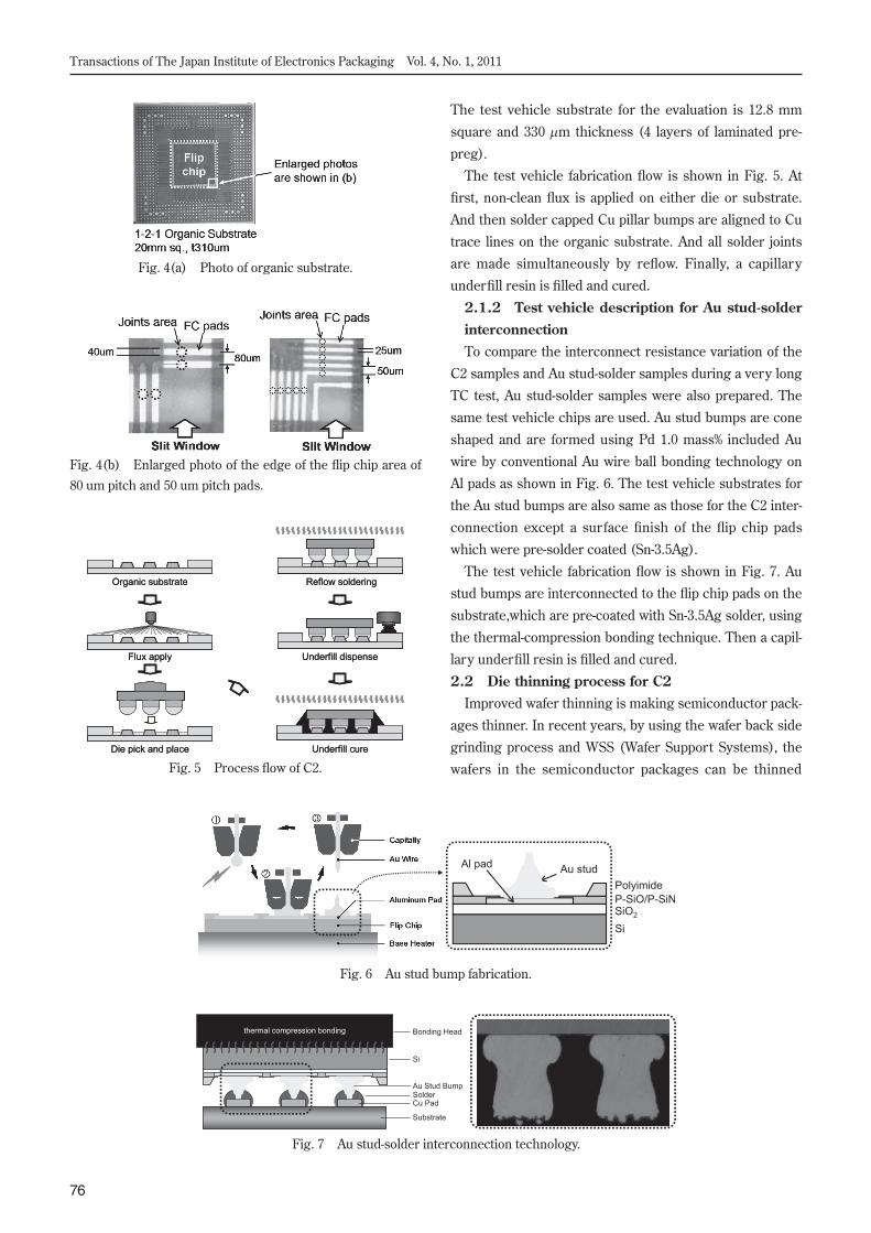
capped Cu pillar bump structure. A SEM (Scanning Elec-
tron Microscope) photo of the bumps is shown in Fig. 3.
The copper pillar height and solder height of C2 bumps
are 45 μm and 25 μm on 80 μm pitch test vehicle chip and
33 μm and 20 μm on 50 μm test vehicle chip. The test vehi-
cle substrates for the evaluation are 20 mm square size
and 310 μm thickness (4 layers of laminated prepreg). A
flip chip can be mounted in the center, and PoP pads (0.5
mm pitch) are located around the flip chip as shown in Fig.
4(a). Solder-resist is opened in the peripheral I/O region
of the die as shown in Fig. 4(b). OSP is applied to the
exposed Cu trace lines to prevent oxidation of Cu. In addi-
tion to non low-k device test die, the low-k device test die
was prepared. The low-k device test die is 6.1 mm square
with the C2 bumps. Each C2 bump consists of a Cu pillar
(25 μm height) and Sn-2.5Ag solder (20 μm height) with
560 staggered bumps in a 60 μm pitch peripheral layout.
Fig. 3 SEM image of 50 um pitch bumps.
Table 1 Comparison of fine-pitch flip chip interconnections.
C2 Interconnection Au stud-solder interconnection
Bumping ProcessSolder capped Cu pillar bump
Electro-Plating on Wafer (Parallel Bumping)
Au stud bump Au wire ball bonding on Die or Wafer
(Serial Bumping)
Solder Pre-coat on Carrier No Required Required
Flip Chip Interconnection Method Pick & Place + Reflow Thermal Compression Bonding
ProductivityHigh
(Short Process Time)Low
(Long Process Time)
Solder Wet-ability Required Flux for Good Wetting Good Wetting Without Flux
Interconnect ion SolderCu, Sn-Ag
(Slow IMC (Sn-Cu) Growth Rate)Au, Sn-Ag
(Fast IMC (Au-Sn) Growth Rate)
Features
- Wafer level operation- One time reflow for flip chip & SMD- Less capital investment- High joint reliability
- Non necessity of Wafer level operation(diced chip can be handles)
76
Transactions of The Japan Institute of Electronics Packaging Vol. 4, No. 1, 2011
The test vehicle substrate for the evaluation is 12.8 mm
square and 330 μm thickness (4 layers of laminated pre-
preg).
The test vehicle fabrication flow is shown in Fig. 5. At
first, non-clean flux is applied on either die or substrate.
And then solder capped Cu pillar bumps are aligned to Cu
trace lines on the organic substrate. And all solder joints
are made simultaneously by reflow. Finally, a capillary
underfill resin is filled and cured.
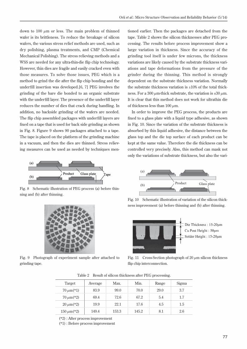
2.1.2 Test vehicle description for Au stud-solder interconnectionTo compare the interconnect resistance variation of the
C2 samples and Au stud-solder samples during a very long
TC test, Au stud-solder samples were also prepared. The
same test vehicle chips are used. Au stud bumps are cone
shaped and are formed using Pd 1.0 mass% included Au
wire by conventional Au wire ball bonding technology on
Al pads as shown in Fig. 6. The test vehicle substrates for
the Au stud bumps are also same as those for the C2 inter-
connection except a surface finish of the flip chip pads
which were pre-solder coated (Sn-3.5Ag).
The test vehicle fabrication flow is shown in Fig. 7. Au
stud bumps are interconnected to the flip chip pads on the
substrate,which are pre-coated with Sn-3.5Ag solder, using
the thermal-compression bonding technique. Then a capil-
lary underfill resin is filled and cured.
2.2 Die thinning process for C2Improved wafer thinning is making semiconductor pack-
ages thinner. In recent years, by using the wafer back side
grinding process and WSS (Wafer Support Systems), the
wafers in the semiconductor packages can be thinned
Fig. 7 Au stud-solder interconnection technology.
Fig. 4(a) Photo of organic substrate.
Fig. 4(b) Enlarged photo of the edge of the flip chip area of 80 um pitch and 50 um pitch pads.
Fig. 5 Process flow of C2.
Fig. 6 Au stud bump fabrication.
77
Orii et al.: Micro Structure Observation and Reliability Behavior (5/14)
down to 100 μm or less. The main problem of thinned
wafer is its brittleness. To reduce the breakage of silicon
wafers, the various stress relief methods are used, such as
dry polishing, plasma treatments, and CMP (Chemical
Mechanical Polishing). The stress relieving methods and a
WSS are needed for any ultra-thin-die flip chip technology.
However, thin dies are fragile and easily cracked even with
those measures. To solve those issues, PEG which is a
method to grind the die after the flip chip bonding and the
underfill insertion was developed.[6, 7] PEG involves the
grinding of the bare die bonded to an organic substrate
with the underfill layer. The presence of the underfill layer
reduces the number of dies that crack during handling. In
addition, no backside grinding of the wafers are needed.
The flip chip assembled packages with underfill layers are
fixed on a tape that is used for back side grinding as shown
in Fig. 8. Figure 9 shows 90 packages attached to a tape.
The tape is placed on the platform of the grinding machine
in a vacuum, and then the dies are thinned. Stress reliev-
ing measures can be used as needed by techniques men-
tioned earlier. Then the packages are detached from the
tape. Table 2 shows the silicon thicknesses after PEG pro-
cessing. The results before process improvement show a
large variation in thickness. Since the accuracy of the
grinding tool itself is under few microns, the thickness
variations are likely caused by the substrate thickness vari-
ations and tape deformations from the pressure of the
grinder during the thinning. This method is strongly
dependent on the substrate thickness variation. Normally
the substrate thickness variation is ±10% of the total thick-
ness. For a 300 μm-thick substrate, the variation is ±30 μm.
It is clear that this method does not work for ultrathin die
of thickness less than 100 μm.
In order to improve the PEG process, the products are
fixed to a glass plate with a liquid type adhesive, as shown
in Fig. 10. Since the variation of the substrate thickness is
absorbed by this liquid adhesive, the distance between the
glass top and the die top surface of each product can be
kept at the same value. Therefore the die thickness can be
controlled very precisely. Also, this method can mask not
only the variations of substrate thickness, but also the vari-
Fig. 8 Schematic illustration of PEG process (a) before thin-ning and (b) after thinning.
Fig. 9 Photograph of experiment sample after attached to grinding tape.
Fig. 10 Schematic illustration of variation of the silicon thick-ness improvement (a) before thinning and (b) after thinning.
Table 2 Result of silicon thickness after PEG processing.
Target Average Max. Min. Range Sigma
70 μm(*1) 83.9 99.0 70.0 29.0 3.7
70 μm(*2) 69.4 72.6 67.2 5.4 1.7
20 μm(*2) 19.9 22.1 17.6 4.5 1.5
150 μm(*2) 149.4 153.3 145.2 8.1 2.6
(*2) : After process improvement(*1) : Before process improvement
Fig. 11 Cross-Section photograph of 20 μm silicon thickness flip chip interconnection.
78
Transactions of The Japan Institute of Electronics Packaging Vol. 4, No. 1, 2011
ations of joint height. The results of this improved method
also appear in Table 2. As shown in the table, the span of
the silicon thickness differences of 29 μm in the first
experiment was reduced to 5.4 μm using this improved
method. Figure 11 shows a cross-section of the 20
μm-thick silicon die flip chip interconnections. This tech-
nique was used to evaluate the C2 flip chip interconnection
with ultra-thin die.
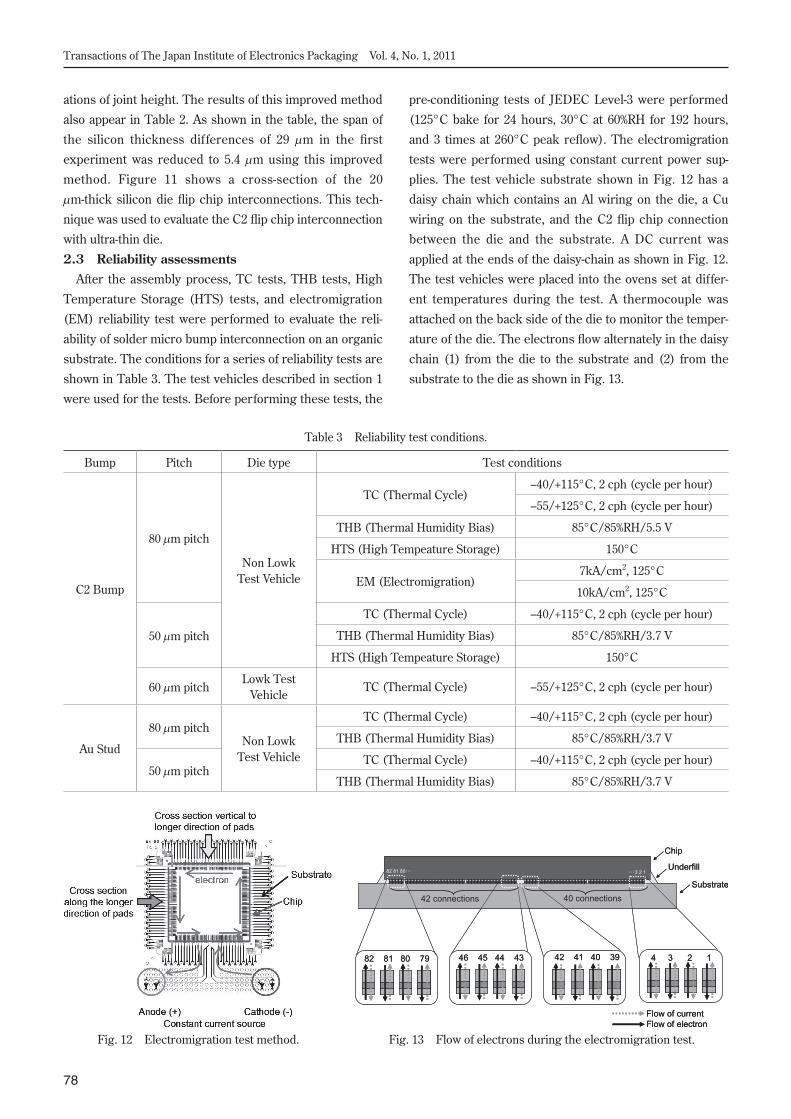
2.3 Reliability assessmentsAfter the assembly process, TC tests, THB tests, High
Temperature Storage (HTS) tests, and electromigration
(EM) reliability test were performed to evaluate the reli-
ability of solder micro bump interconnection on an organic
substrate. The conditions for a series of reliability tests are
shown in Table 3. The test vehicles described in section 1
were used for the tests. Before performing these tests, the
pre-conditioning tests of JEDEC Level-3 were performed
(125°C bake for 24 hours, 30°C at 60%RH for 192 hours,
and 3 times at 260°C peak reflow). The electromigration
tests were performed using constant current power sup-
plies. The test vehicle substrate shown in Fig. 12 has a
daisy chain which contains an Al wiring on the die, a Cu
wiring on the substrate, and the C2 flip chip connection
between the die and the substrate. A DC current was
applied at the ends of the daisy-chain as shown in Fig. 12.
The test vehicles were placed into the ovens set at differ-
ent temperatures during the test. A thermocouple was
attached on the back side of the die to monitor the temper-
ature of the die. The electrons flow alternately in the daisy
chain (1) from the die to the substrate and (2) from the
substrate to the die as shown in Fig. 13.
Fig. 12 Electromigration test method. Fig. 13 Flow of electrons during the electromigration test.
Table 3 Reliability test conditions.
Bump Pitch Die type Test conditions
C2 Bump
80 μm pitch
Non Lowk Test Vehicle
TC (Thermal Cycle)–40/+115°C, 2 cph (cycle per hour)
–55/+125°C, 2 cph (cycle per hour)
THB (Thermal Humidity Bias) 85°C/85%RH/5.5 V
HTS (High Tempeature Storage) 150°C
EM (Electromigration)7kA/cm2, 125°C
10kA/cm2, 125°C
50 μm pitch
TC (Thermal Cycle) –40/+115°C, 2 cph (cycle per hour)
THB (Thermal Humidity Bias) 85°C/85%RH/3.7 V
HTS (High Tempeature Storage) 150°C
60 μm pitchLowk Test
VehicleTC (Thermal Cycle) –55/+125°C, 2 cph (cycle per hour)
Au Stud
80 μm pitchNon Lowk
Test Vehicle
TC (Thermal Cycle) –40/+115°C, 2 cph (cycle per hour)
THB (Thermal Humidity Bias) 85°C/85%RH/3.7 V
50 μm pitchTC (Thermal Cycle) –40/+115°C, 2 cph (cycle per hour)
THB (Thermal Humidity Bias) 85°C/85%RH/3.7 V
79
Orii et al.: Micro Structure Observation and Reliability Behavior (7/14)
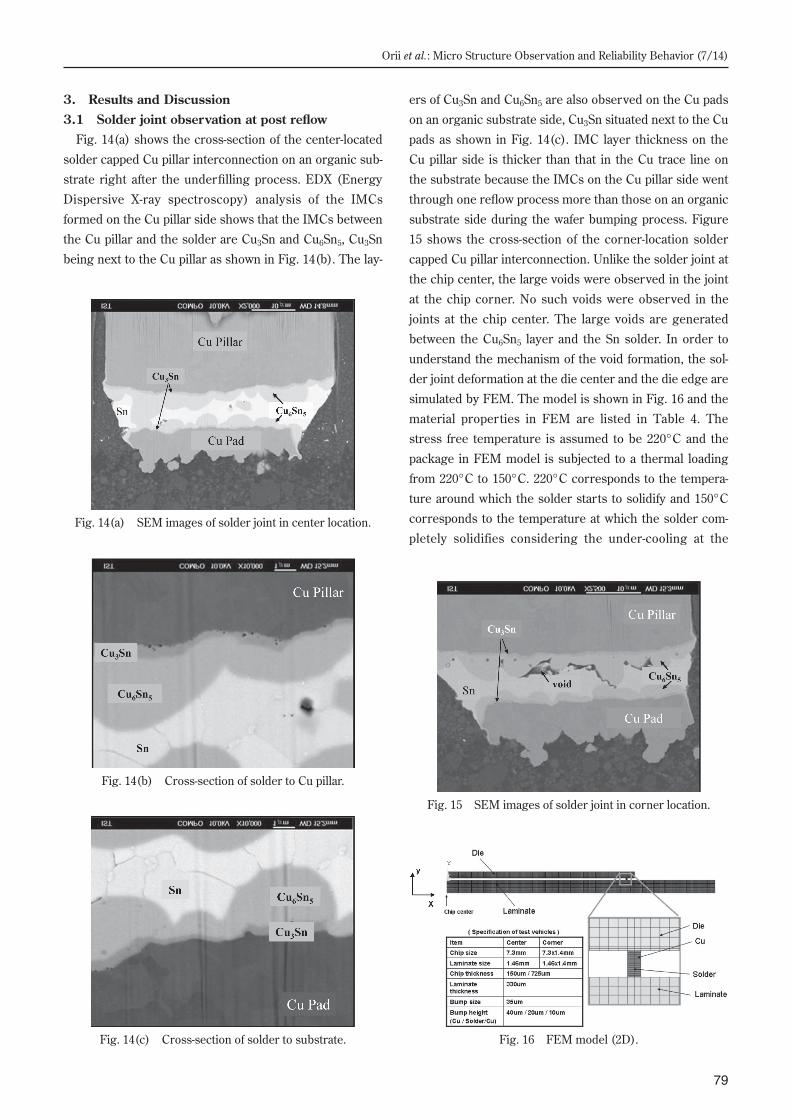
3. Results and Discussion3.1 Solder joint observation at post reflow
Fig. 14(a) shows the cross-section of the center-located
solder capped Cu pillar interconnection on an organic sub-
strate right after the underfilling process. EDX (Energy
Dispersive X-ray spectroscopy) analysis of the IMCs
formed on the Cu pillar side shows that the IMCs between
the Cu pillar and the solder are Cu3Sn and Cu6Sn5, Cu3Sn
being next to the Cu pillar as shown in Fig. 14(b). The lay-
ers of Cu3Sn and Cu6Sn5 are also observed on the Cu pads
on an organic substrate side, Cu3Sn situated next to the Cu
pads as shown in Fig. 14(c). IMC layer thickness on the
Cu pillar side is thicker than that in the Cu trace line on
the substrate because the IMCs on the Cu pillar side went
through one reflow process more than those on an organic
substrate side during the wafer bumping process. Figure
15 shows the cross-section of the corner-location solder
capped Cu pillar interconnection. Unlike the solder joint at
the chip center, the large voids were observed in the joint
at the chip corner. No such voids were observed in the
joints at the chip center. The large voids are generated
between the Cu6Sn5 layer and the Sn solder. In order to
understand the mechanism of the void formation, the sol-
der joint deformation at the die center and the die edge are
simulated by FEM. The model is shown in Fig. 16 and the
material properties in FEM are listed in Table 4. The
stress free temperature is assumed to be 220°C and the
package in FEM model is subjected to a thermal loading
from 220°C to 150°C. 220°C corresponds to the tempera-
ture around which the solder starts to solidify and 150°C
corresponds to the temperature at which the solder com-
pletely solidifies considering the under-cooling at the Fig. 14(a) SEM images of solder joint in center location.
Fig. 14(b) Cross-section of solder to Cu pillar.
Fig. 14(c) Cross-section of solder to substrate.
Fig. 15 SEM images of solder joint in corner location.
Fig. 16 FEM model (2D).
80
Transactions of The Japan Institute of Electronics Packaging Vol. 4, No. 1, 2011
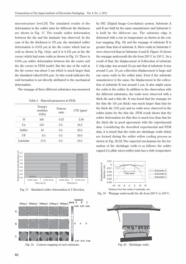
microstructure level.[8] The simulated results of the
deformation in the solder joint for different die thickness
are shown in Fig. 17. The tensile solder deformation
between the die and the laminate was observed. In the
case of the die thickness is 725 μm, the simulated solder
deformation is 0.078 μm at the die center which had no
void as shown in Fig. 14(a), and it is 0.132 μm at the die
corner which had some voids as shown in Fig. 15. There is
0.054 μm solder deformation between the die center and
the die corner in FEM model. But the size of the void at
the die corner was about 3 um which is much larger than
the simulated value(0.054 μm). So this result indicates the
void formation is not directly attributed to the mechanical
deformation.
The warpage of three different substrates was measured
by DIC (Digital Image Correlation) system. Substrate A
and B are built by the same manufacturer and Substrate C
is built by the dif ferent one. The substrate edge is
deformed with a rise in temperature as shown in the con-
tour mapping (Fig. 18) and the warpage of substrate B is
greater than that of substrate A. More voids in Substrate C
were observed than in Substrate A and B. Figure 19 shows
the warpage underneath the die from 220°C to 150°C. As a
result of that, the displacement of Z-direction of substrate
C chip edge was around 10 μm and that of substrate A was
around 2 μm. 10 μm z-direction displacement is large and
can cause voids in the solder joint. Even if the substrate
manufacturer is the same, the displacement in the z-direc-
tion of substrate B was around 5 μm. It also might cause
the voids in the solder. In addition to the observation with
the different substrates, the voids were observed with a
thick die and a thin die. It was found that the warpage for
the thin die (10 μm thick) was much larger than that for
the thick die (725 μm) and no voids were observed in the
solder joints for the thin die. FEM result shows that the
solder deformation for thin dies is much less than that for
the thick die in good agreement with the experimental
data. Considering the described experimental and FEM
data, it is found that the voids are shrinkage voids which
are formed during the solder reflow cooling process as
shown in Fig. 20.[9] The expected mechanism for the for-
mation of the shrinkage voids is as follows: the solder
capped Cu pillar micro-solder joint has a wide temperature
Fig. 17 Simulated solder deformation in Y direction.
Fig. 18 Contour mapping of each substrate.
Fig. 19 Warpage underneath the die from 220°C to 150°C.
Fig. 20 Shrinkage voids.
Table 4 Material parameters in FEM.
Young’s modulus
(GPa)
Poisron ratio
CTE (ppm)
Si 160 0.23 2.56
Cu 110 0.3 16.2
Solder 10 0.3 23.0
UF 8.5 0.3 30.0
Laminate 17.6 0.3 16.0
81
Orii et al.: Micro Structure Observation and Reliability Behavior (9/14)
range of liquid phase because of the under-cooling acceler-
ated by the small size of the micro-solder joint. Solder
capped Cu pillar joint was made by reflow and at the cool-
ing process the shrinkage voids are expected to be formed
by the substrate warpage during the wide range tempera-
ture at the liquid phase of the Sn-Ag-Cu solder joint and
the volumetric contraction of the solder. As a result of the
experimental data, the shrinkage voids are strongly depen-
dent on the substrate warpage.
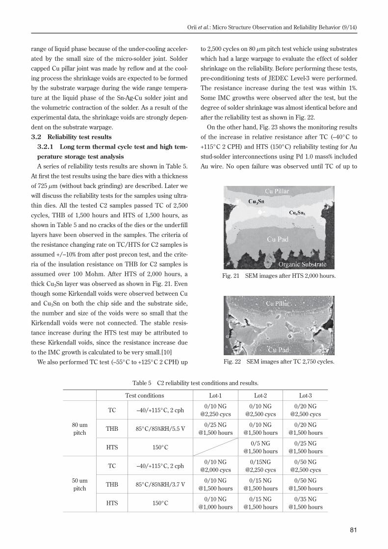
3.2 Reliability test results3.2.1 Long term thermal cycle test and high tem-perature storage test analysisA series of reliability tests results are shown in Table 5.
At first the test results using the bare dies with a thickness
of 725 μm (without back grinding) are described. Later we
will discuss the reliability tests for the samples using ultra-
thin dies. All the tested C2 samples passed TC of 2,500
cycles, THB of 1,500 hours and HTS of 1,500 hours, as
shown in Table 5 and no cracks of the dies or the underfill
layers have been observed in the samples. The criteria of
the resistance changing rate on TC/HTS for C2 samples is
assumed +/–10% from after post precon test, and the crite-
ria of the insulation resistance on THB for C2 samples is
assumed over 100 Mohm. After HTS of 2,000 hours, a
thick Cu3Sn layer was observed as shown in Fig. 21. Even
though some Kirkendall voids were observed between Cu
and Cu3Sn on both the chip side and the substrate side,
the number and size of the voids were so small that the
Kirkendall voids were not connected. The stable resis-
tance increase during the HTS test may be attributed to
these Kirkendall voids, since the resistance increase due
to the IMC growth is calculated to be very small.[10]
We also performed TC test (–55°C to +125°C 2 CPH) up
to 2,500 cycles on 80 μm pitch test vehicle using substrates
which had a large warpage to evaluate the effect of solder
shrinkage on the reliability. Before performing these tests,
pre-conditioning tests of JEDEC Level-3 were performed.
The resistance increase during the test was within 1%.
Some IMC growths were observed after the test, but the
degree of solder shrinkage was almost identical before and
after the reliability test as shown in Fig. 22.
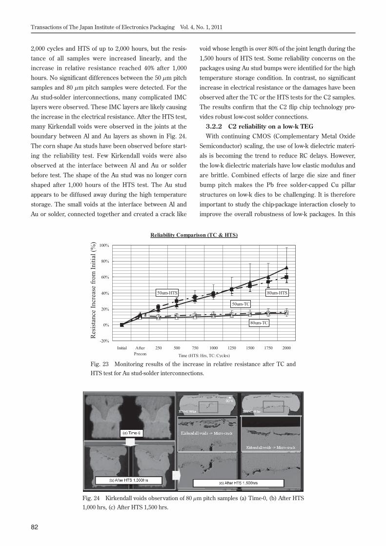
On the other hand, Fig. 23 shows the monitoring results
of the increase in relative resistance after TC (–40°C to
+115°C 2 CPH) and HTS (150°C) reliability testing for Au
stud-solder interconnections using Pd 1.0 mass% included
Au wire. No open failure was observed until TC of up to
Fig. 21 SEM images after HTS 2,000 hours.
Fig. 22 SEM images after TC 2,750 cycles.
Table 5 C2 reliability test conditions and results.
Test conditions Lot-1 Lot-2 Lot-3
80 um pitch
TC –40/+115°C, 2 cph0/10 NG
@2,250 cycs0/10 NG
@2,500 cycs0/20 NG
@2,500 cycs
THB 85°C/85%RH/5.5 V0/25 NG
@1,500 hours0/10 NG
@1,500 hours0/20 NG
@1,500 hours
HTS 150°C0/5 NG
@1,500 hours0/25 NG
@1,500 hours
50 um pitch
TC –40/+115°C, 2 cph0/10 NG
@2,000 cycs0/15NG
@2,250 cycs0/50 NG
@2,500 cycs
THB 85°C/85%RH/3.7 V0/10 NG
@1,500 hours0/15 NG
@1,500 hours0/50 NG
@1,500 hours
HTS 150°C0/10 NG
@1,000 hours0/15 NG
@1,500 hours0/35 NG
@1,500 hours
82
Transactions of The Japan Institute of Electronics Packaging Vol. 4, No. 1, 2011
2,000 cycles and HTS of up to 2,000 hours, but the resis-
tance of all samples were increased linearly, and the
increase in relative resistance reached 40% after 1,000
hours. No significant differences between the 50 μm pitch
samples and 80 μm pitch samples were detected. For the
Au stud-solder interconnections, many complicated IMC
layers were observed. These IMC layers are likely causing
the increase in the electrical resistance. After the HTS test,
many Kirkendall voids were observed in the joints at the
boundary between Al and Au layers as shown in Fig. 24.
The corn shape Au studs have been observed before start-
ing the reliability test. Few Kirkendall voids were also
observed at the interface between Al and Au or solder
before test. The shape of the Au stud was no longer corn
shaped after 1,000 hours of the HTS test. The Au stud
appears to be diffused away during the high temperature
storage. The small voids at the interface between Al and
Au or solder, connected together and created a crack like
void whose length is over 80% of the joint length during the
1,500 hours of HTS test. Some reliability concerns on the
packages using Au stud bumps were identified for the high
temperature storage condition. In contrast, no significant
increase in electrical resistance or the damages have been
observed after the TC or the HTS tests for the C2 samples.
The results confirm that the C2 flip chip technology pro-
vides robust low-cost solder connections.
3.2.2 C2 reliability on a low-k TEGWith continuing CMOS (Complementary Metal Oxide
Semiconductor) scaling, the use of low-k dielectric materi-
als is becoming the trend to reduce RC delays. However,
the low-k dielectric materials have low elastic modulus and
are brittle. Combined effects of large die size and finer
bump pitch makes the Pb free solder-capped Cu pillar
structures on low-k dies to be challenging. It is therefore
important to study the chip-package interaction closely to
improve the overall robustness of low-k packages. In this
Fig. 23 Monitoring results of the increase in relative resistance after TC and HTS test for Au stud-solder interconnections.
Fig. 24 Kirkendall voids observation of 80 μm pitch samples (a) Time-0, (b) After HTS 1,000 hrs, (c) After HTS 1,500 hrs.
83
Orii et al.: Micro Structure Observation and Reliability Behavior (11/14)
section, the affinity of the C2 structure for the systems
with low-k materials was evaluated. The low-k device test
die description is written in section 2.1.1. JEDEC Level-3
pre-conditioning and TC tests (–55°C to +125°C, 2 CPH)
were performed. No failures were observed up to 1,500
cycles. The cross-section of the C2 joint after 1,000 cycles
of test is shown in Fig. 25. No damages have been
observed for these joints. The results show that the low-k
C2 structures seem robust for die sizes of 6 mm or less.
Our next tests will be an evaluation of the C2 bump struc-
tures on a larger die.
3.2.3 Cu pillar-solder structure with ultra thin dieThe same test vehicles as noted in test vehicle section
were used for this evaluation. Only TC tests (–40°C to
+115°C, 2 CPH) were done with the thin dies. Four differ-
ent thicknesses of silicon dies, 20 μm, 70 μm, 150 μm and
725 μm, were joined on organic substrates with the C2
technology with PEG technique. One 725 μm sample out
of eight failed at 4,000 cycles. Although the other seven
725 μm samples passed the test, their resistance increased
somewhat. The resistances of the other die thicknesses
were very stable and the ratio of increased resistance was
less than 2% over 8,500 cycles as shown in Fig. 26. One of
the concerned failure modes for such thin dies was a die
crack due to PEG process. However, there were no fail-
ures of that mode. This reliability test results in confirming
that “when a die is thin, the strain on its joints is small”.
3.2.4 Structure analysis on the low-k stress and the solder joint strainFEM simulation was performed to investigate the effect
of the die thickness on the substrate warpage and the sol-
der joint strain over the temperature range from 220°C to
–55°C. Figure 27 shows the maximum substrate warpage
is 87 μm for a die thickness of 725 μm and 437 μm for a die
thickness of 50 μm. When the die is thick, the hard silicon
limits the warpage of the substrate. Conversely, when the
die is thin, it cannot resist warping of the substrate and
Fig. 25 60 um pitch C2 flip chip interconnection with low-k device.
Fig. 26 Result of thermal cycling test.
Fig. 27 Effect of chip thickness on substrate warpage and solder strain.
84
Transactions of The Japan Institute of Electronics Packaging Vol. 4, No. 1, 2011
then the warpage is large. At the same time, the strain on
the solder joints is reduced when the die is thin. The strain
is 4.19 × 10⁻³ for a die thickness of 725 μm and 3.23 × 10⁻³
for 50 μm. This simulation results are in good agreement
with the experimental data that the thicker chip package
had earlier solder joint fatigue failure than thinner one.
To study the effect of Cu pillar to solder height ratio on
low-k stress and solder joint strain, the simulation was con-
ducted by the FEM model which had no underfill material
over the temperature range from 220°C to 25°C. Figure 28
shows that the lower Cu pillar height is suitable for the
low-k stress reduction. From the electromigration point of
view, the Cu pillar is beneficial for solder electromigration
lifetime improvement. So it is important to determine the
Cu pillar height considering both the low-k stress and the
electromigration performance.
3.3 Electromigration 3.3.1 Electromigration test resultsDuring the electromigration test, the electrical resis-
tance variation was monitored in-situ using test vehicles.
The variations of electrical resistance during the test were
less than 1% for all the samples as shown in Fig. 29. The
failure criterion is 10% resistance variation from the initial
resistance value. From these figures, no failure data was
recorded up to 1,000 hours. The EPMA analyses of the
cross-sections of the Sn-2.5Ag solder joints without Ni bar-
riers or thermal aging were performed to observe the IMC
growth and the dissolution of Cu atoms into the solder.
The results before and after the electromigration test are
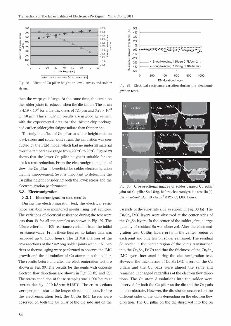
shown in Fig. 30. The results for the joints with opposite
electron flow directions are shown in Fig. 30 (b) and (c).
The stress condition of these samples was 1,000 hours at
current density of 10 kA/cm2@125°C. The cross-sections
were perpendicular to the longer direction of pads. Before
the electromigration test, the Cu3Sn IMC layers were
observed on both the Cu pillar of the die side and on the
Cu pads of the substrate side as shown in Fig. 30 (a). The
Cu6Sn5 IMC layers were observed at the center sides of
the Cu3Sn layers. In the center of the solder joint, a large
quantity of residual Sn was observed. After the electromi-
gration test, Cu6Sn5 layers grew in the center region of
each joint and only few Sn solder remained. The residual
Sn solder in the center region of the joints transformed
into the Cu6Sn5 IMCs and that the thickness of the Cu6Sn5
IMC layers increased during the electromigration test.
However the thicknesses of Cu3Sn IMC layers on the Cu
pillars and the Cu pads were almost the same and
remained unchanged regardless of the electron flow direc-
tions. The Cu atom dissolutions into the solder were
observed for both the Cu pillar on the die and the Cu pads
on the substrate. However, the dissolution occurred on the
different sides of the joints depending on the electron flow
direction. The Cu pillar on the die dissolved into the Sn
Fig. 28 Effect of Cu pillar height on low-k stress and solder strain.
Fig. 29 Electrical resistance variation during the electromi-gration tests.
Fig. 30 Cross-sectional images of solder capped Cu pillar joint (a) Cu pillar-Sn-2.5Ag, before electromigration test (b)(c) Cu pillar-Sn-2.5Ag, 10 kA/cm2@125°C, 1,000 hours.
85
Orii et al.: Micro Structure Observation and Reliability Behavior (13/14)
solder only when the electron flew from the die to the sub-
strate as shown in Fig. 30 (b). The Cu pad dissolution
occurred when the electrons flew from the substrate to the
die. This is because the Cu metals in the Cu pad dissolve
into the Sn solder more in the direction of the electron
flow than in the opposite direction as shown in Fig. 30(c).
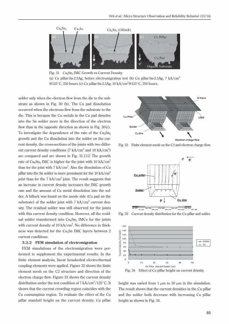
To investigate the dependence of the rate of the Cu6Sn5
growth and the Cu dissolution into the solder on the cur-
rent density, the cross-sections of the joints with two differ-
ent current density conditions (7 kA/cm2 and 10 kA/cm2)
are compared and are shown in Fig. 31.[11] The growth
rate of Cu6Sn5 IMC is higher for the joint with 10 kA/cm2
than for the joint with 7 kA/cm2. Also the dissolution of Cu
pillar into the Sn solder is more prominent for the 10 kA/cm2
joint than for the 7 kA/cm2 joint. The result suggests that
an increase in current density increases the IMC growth
rate and the amount of Cu metal dissolution into the sol-
der. A hillock was found on the anode side (Cu pad on the
substrate) of the solder joint with 7 kA/cm2 current den-
sity. The residual solder was still observed for the joints
with this current density condition. However, all the resid-
ual solder transformed into Cu6Sn5 IMCs for the joints
with current density of 10 kA/cm2. No difference in thick-
ness was detected for the Cu3Sn IMC layers between 2
current conditions.
3.3.2 FEM simulation of electromigrationFEM simulations of the electromigration were per-
formed to supplement the experimental results. In the
finite element analysis, linear hexahedral electro-thermal
coupling elements were applied. Figure 32 shows the finite
element mesh on the C2 structure and direction of the
electron charge flow. Figure 33 shows the current density
distribution under the test condition of 7 kA/cm2/125°C. It
shows that the current crowding region coincides with the
Cu consumption region. To evaluate the effect of the Cu
pillar standoff height on the current density, Cu pillar
height was varied from 1 μm to 50 μm in the simulation.
The result shows that the current densities in the Cu pillar
and the solder both decrease with increasing Cu pillar
height as shown in Fig. 34.
Fig. 31 Cu6Sn5 IMC Growth vs Current Density.(a) Cu pillar-Sn-2.5Ag, before electromigration test (b) Cu pillar-Sn-2.5Ag, 7 kA/cm2
@125°C, 250 hours (c) Cu pillar-Sn-2.5Ag, 10 kA/cm2@125°C, 250 hours.
Fig. 32 Finite element mesh on the C2 and electron charge flow.
Fig. 33 Current density distribution for the Cu pillar and solder.
Fig. 34 Effect of Cu pillar height on current density.
86
Transactions of The Japan Institute of Electronics Packaging Vol. 4, No. 1, 2011
4. ConclusionsThe C2 using the solder capped Cu pillar bumps is a flip
chip interconnection method designed for the wire-bond-
ing technology with a pitch of 50 μm or larger. Since the
process is C4 and SMT compatible, it is an inexpensive
method and the current C4 and SMT infrastructures can
be utilized. Many voids in the solder joint at the chip edge
were observed after the reflow process. These voids are
supposed to be the shrinkage voids caused by the wide
range of the solder liquid phase and the substrate warp-
age. Since they are not the stress induced voids, it was
confirmed that they didn’t affect the reliability test. The C2
interconnection resistance increase after the thermal
cycles and high temperature storage is quite small com-
pared to Au stud-solder interconnections. Also the C2
structure was evaluated for a low-k device and no failures
were observed at 1,500 cycles in the thermal cycle test.
The electromigration tests showed that the C2 structure
has high endurance against electromigration and no fail-
ure data was recorded until 1,000 hours with several elec-
tromigration conditions regardless the direction of elec-
tron flow. This indicates that the C2 structure is very
robust. However, if one considers the stress on the low-k
materials, the Cu pillar structure has a disadvantage in
comparison with the traditional solder joint. FEM simula-
tion shows that reducing the Cu pillar height can reduce
the stress on the low-k materials. From the electromigra-
tion point of view, an increase in the Cu pillar height can
reduce the effect of the current crowding in the joints. A
careful optimization of the joint structure is necessary
including the Cu pillar height, in order to simultaneously
realize the low-k stress reduction and the formation of the
electromigration resistant joints. CPI (Chip Package Inter-
action),[12] which is the interaction between the semicon-
ductor package stresses and the semiconductor device,
becomes more important and the flip chip interconnection
structure and its joint material optimization must continue
to be discussed for the future more complicated packaging
such as 3D-IC.
References[1] T. Maeda, “3-Dimensional Package on Package
Mounting Process by STAMP,” Journal of Japan
Institute of Electronics Packaging, No. 3, 2005 (in
Japanese).
[2] K. Fujita and T. Kamiyoshi, “Three-Dimensional Sys-
tem in Packaging Technology,” Sharp Technology
Report, No. 83, 2002.
[3] Y. Yoneda, T. Kuramochi, T. Sohara, and J. M. Liao,
“A Novel Flip Chip Bonding Technology Using Au
Stud Bump and Lead-Free Solder,” Pan-Pacific Con-
ference, 1999.
[4] Y. Orii, K. Toriyama, Y. Oyama, and T. Nishio, “Ultra-
thin SiP/PoP Technologies using 50 μm pitch C4
interconnections,” Proceedings of the International
Conference on Electronics Packaging, pp. 66–71, 2007.
[5] K. Toriyama and Y. Orii, “Development of Fine Pitch
Flip Chip Interconnection Using Solder Bumps,”
Proceedings of the Microelectronics Symposium, pp.
143–146, 2007 (in Japanese).
[6] Y. Orii, K. Toriyama, Y. Oyama, and T. Nishio, “Post
Encapsulation Grinding for MPS-C2 Ultrafine Pitch
Flip Chip Technology,” Proceedings of the Interna-
tional Conference on Electronics Packaging, pp. 188–
193, 2008.
[7] Y. Orii, K. Toriyama, Y. Oyama, and T. Nakanishi,
“Development of Solder Interconnection in Ultra
Thin SiP/PoP,” National Convention of I.E.E. Japan,
Vol. 3, 3–S16(21)–(24), 2006 (in Japanese).
[8] R. Kinyanjuia, L. P. Lehmana, L. Zavalija, and E.
Cottsa, “Effect of Sample Size on the Solidification
Temperature and Microstructure of SnAgCu Near
Eutectic Alloys,” Journal of Materials Research, Vol.
20, pp. 2914–2918, 2005.
[9] Y. Orii, K. Toriyama, H. Noma, and K. Uenishi, “Sol-
der alloy observation and its reliability of ultra fine
pitch peripheral flip chip interconnection with Cu
post bumps,” Microjoining and Assembly Technol-
ogy in Electronics Symposium, pp. 59–62, 2011 (in
Japanese).
[10] S. Jeong, N. Murata, Y. Sato, K. Suzuki, and H. Miura,
“Effect of the Formation of the Intermetallic Com-
pounds between a Tin Bump and an Electroplated
Copper Thin Film on both the Mechanical and Elec-
trical Properties of the Jointed Structures,” Transac-
tions of The Japan Institute of Electronics Packaging,
Vol. 2, No. 1, pp. 91–97, 2009.
[11] Y. Orii, K. Toriyama, S. Kohara, H. Noma, K. Okamoto,
D. Toyoshima, and K. Uenishi, “Electromigration
analysis of peripheral ultra fine pitch C2 flip chip
interconnection with solder capped Cu pillar bump,”
The 61st Electronic Components and Technology
Conference (ECTC), pp. 340–345, 2001.
[12] JEDEC, JEP156: “Chip-Package Interaction Under-
standing, Identification and Evaluation,” 2009.


![Impacts of Operators’ Behavior on Reliability of Power ...mahshidr.myweb.usf.edu/Files/Publications/PDFs/PowerTrans2018.pdf · reliability of power-grid operations [5]–[9]. It](https://img.pdfslide.tips/doc/110x75/5f95dee128e1c1260c17f627/impacts-of-operatorsa-behavior-on-reliability-of-power-reliability-of-power-grid.jpg)