Embed Size (px)
Citation preview
Mikroskopia sił atomowychAtomic Force Microscope AFM
• Zasada działania• Historia ‘odkryć’• Zastosowane rozwiązania• Przykłady zastosowań
Bolesław AUGUSTYNIAK
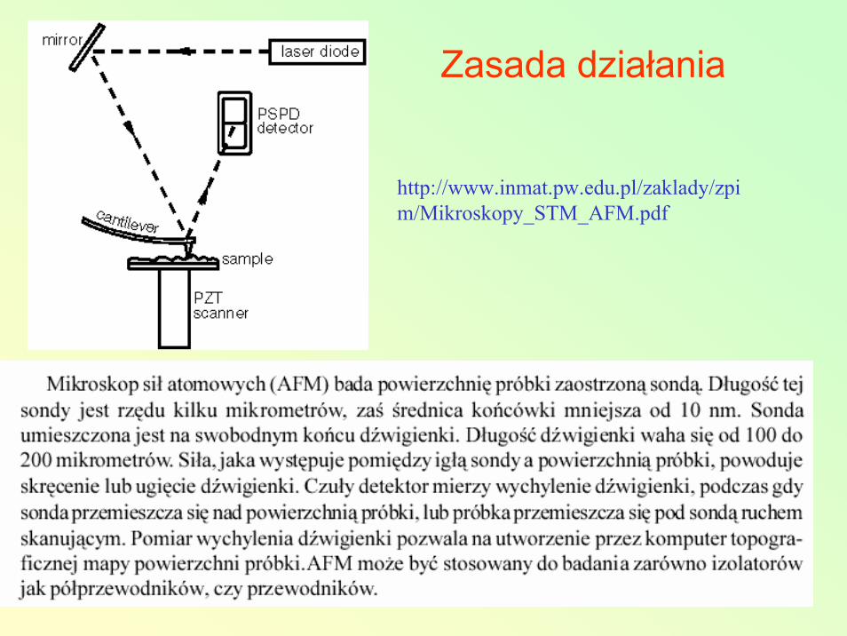
Zasada działania
http://www.inmat.pw.edu.pl/zaklady/zpim/Mikroskopy_STM_AFM.pdf
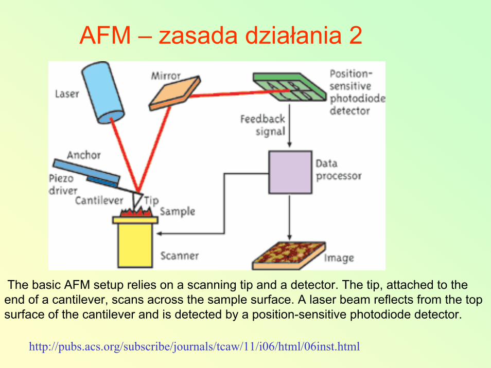
AFM – zasada działania 2
The basic AFM setup relies on a scanning tip and a detector. The tip, attached to the end of a cantilever, scans across the sample surface. A laser beam reflects from the topsurface of the cantilever and is detected by a position-sensitive photodiode detector.
http://pubs.acs.org/subscribe/journals/tcaw/11/i06/html/06inst.html
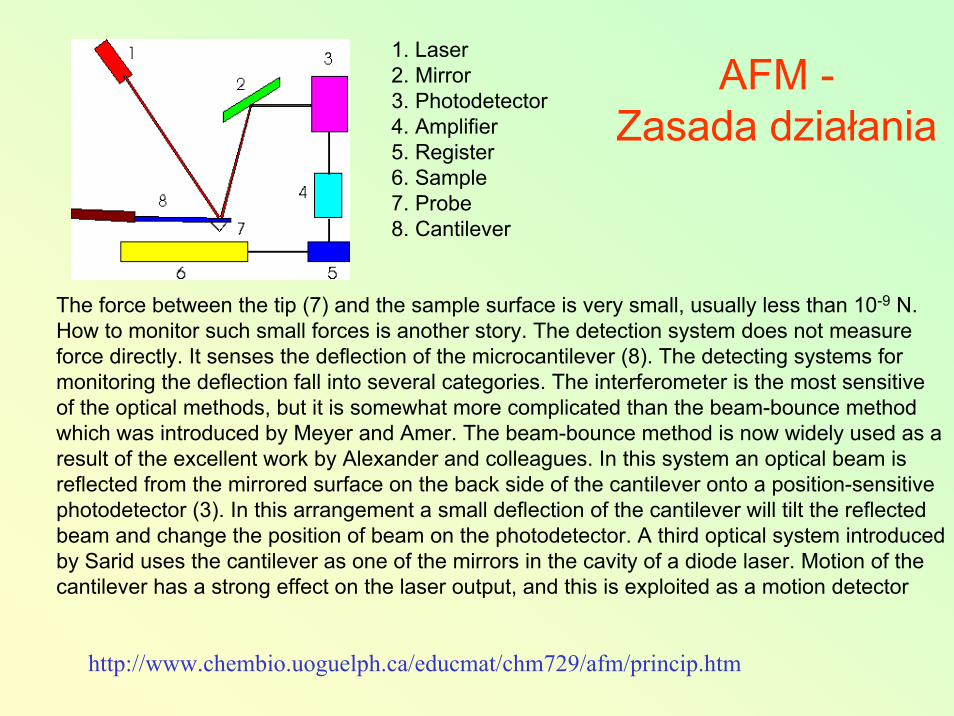
AFM -Zasada działania
http://www.chembio.uoguelph.ca/educmat/chm729/afm/princip.htm
1. Laser 2. Mirror 3. Photodetector 4. Amplifier 5. Register 6. Sample 7. Probe 8. Cantilever
The force between the tip (7) and the sample surface is very small, usually less than 10-9 N.How to monitor such small forces is another story. The detection system does not measure force directly. It senses the deflection of the microcantilever (8). The detecting systems formonitoring the deflection fall into several categories. The interferometer is the most sensitive of the optical methods, but it is somewhat more complicated than the beam-bounce method which was introduced by Meyer and Amer. The beam-bounce method is now widely used as aresult of the excellent work by Alexander and colleagues. In this system an optical beam is reflected from the mirrored surface on the back side of the cantilever onto a position-sensitive photodetector (3). In this arrangement a small deflection of the cantilever will tilt the reflected beam and change the position of beam on the photodetector. A third optical system introducedby Sarid uses the cantilever as one of the mirrors in the cavity of a diode laser. Motion of the cantilever has a strong effect on the laser output, and this is exploited as a motion detector
Historia odkrycia AFMThe first AFM was made by meticulously gluing a tiny shard of diamond onto oneend of a tiny strip of gold foil. In the fall of 1985 Gerd Binnig and Christoph Gerberused the cantilever to examine insulating surfaces. A small hook at the end of the cantilever was pressed against the surface while the sample was scanned beneath the tip. The force between tip and sample was measured by tracking the deflection of the cantilever. This was done by monitoring the tunneling current tot a second tip positioned above the cantilever. They could delineate lateral features as small as 300 Å. The force microscope emerged in this way. In fact, without the breakthrough in tip manufacture, the AFM probably would have remained a curiosity in many research groups. It was Albrecht, a fresh graduate student, who fabricated the first silicon microcantilever and measured the atomic structure of boron nitride. Today the tip-cantilever assembly typically is microfabricated from Si or Si3N4.
http://www.chembio.uoguelph.ca/educmat/chm729/afm/introdn.htm
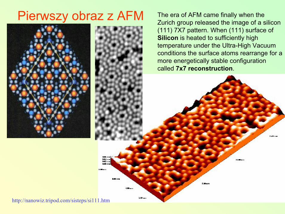
Pierwszy obraz z AFM The era of AFM came finally when the Zurich group released the image of a silicon(111) 7X7 pattern. When (111) surface of Silicon is heated to sufficiently high temperature under the Ultra-High Vacuum conditions the surface atoms rearrange for amore energetically stable configuration called 7x7 reconstruction.
http://nanowiz.tripod.com/sisteps/si111.htm
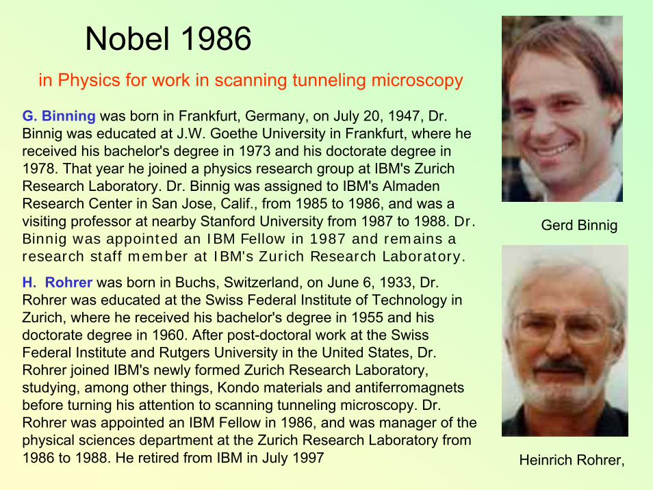
Nobel 1986
Gerd Binnig
Heinrich Rohrer,
in Physics for work in scanning tunneling microscopy
G. Binning was born in Frankfurt, Germany, on July 20, 1947, Dr.Binnig was educated at J.W. Goethe University in Frankfurt, where he received his bachelor's degree in 1973 and his doctorate degree in1978. That year he joined a physics research group at IBM's Zurich Research Laboratory. Dr. Binnig was assigned to IBM's Almaden Research Center in San Jose, Calif., from 1985 to 1986, and was avisiting professor at nearby Stanford University from 1987 to 1988. Dr.Binnig was appointed an IBM Fellow in 1987 and remains aresearch staff member at IBM's Zurich Research Laboratory.
H. Rohrer was born in Buchs, Switzerland, on June 6, 1933, Dr.Rohrer was educated at the Swiss Federal Institute of Technology in Zurich, where he received his bachelor's degree in 1955 and his doctorate degree in 1960. After post-doctoral work at the Swiss Federal Institute and Rutgers University in the United States, Dr.Rohrer joined IBM's newly formed Zurich Research Laboratory,studying, among other things, Kondo materials and antiferromagnets before turning his attention to scanning tunneling microscopy. Dr.Rohrer was appointed an IBM Fellow in 1986, and was manager of the physical sciences department at the Zurich Research Laboratory from1986 to 1988. He retired from IBM in July 1997
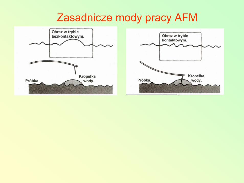
Zasadnicze mody pracy AFM
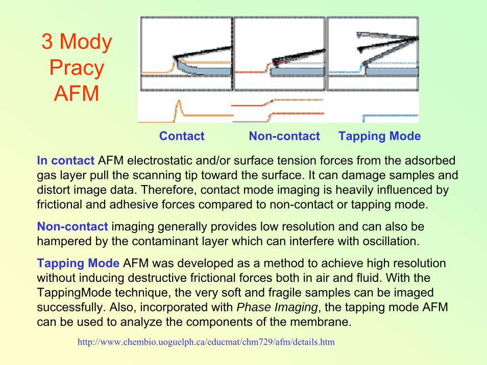
3 Mody Pracy AFM
http://www.chembio.uoguelph.ca/educmat/chm729/afm/details.htm
In contact AFM electrostatic and/or surface tension forces from the adsorbed gas layer pull the scanning tip toward the surface. It can damage samples and distort image data. Therefore, contact mode imaging is heavily influenced byfrictional and adhesive forces compared to non-contact or tapping mode.
Non-contact imaging generally provides low resolution and can also behampered by the contaminant layer which can interfere with oscillation.
Tapping Mode AFM was developed as a method to achieve high resolution without inducing destructive frictional forces both in air and fluid. With the TappingMode technique, the very soft and fragile samples can be imaged successfully. Also, incorporated with Phase Imaging, the tapping mode AFMcan be used to analyze the components of the membrane.
Contact Non-contact Tapping Mode
Phase imagingPhase Imaging is a powerful extension of Tapping Mode Atomic Force Microscopy (AFM) that provides nanometer-scale information about surface structure often not revealed by other SPM techniques. By mapping the phase of the cantilever oscillation during the TappingMode scan, phase imaging goes beyond simple topographical mapping to detect variations in composition,adhesion, friction, viscoelasticity, and perhaps other properties.
In TappingMode AFM, the cantilever is excited into resonance oscillation with apiezoelectric driver. The oscillation amplitude is used as a feedback signal tomeasure topographic variations of the sample. In phase imaging, the phase lagof the cantilever oscillation, relative to the signal sent to the cantilever's piezo driver, is simultaneously monitored by the Extender Electronics Module and recorded by the NanoScope III SPM controller. The phase lag is very sensitiveto variations in material properties such as adhesion and viscoelasticity.

AFM - siły oddziaływania
http://www.inmat.pw.edu.pl/zaklady/zpim/Mikroskopy_STM_AFM.pdf
Ad ‘tapping mode’
http://www.inmat.pw.edu.pl/zaklady/zpim/Mikroskopy_STM_AFM.pdf
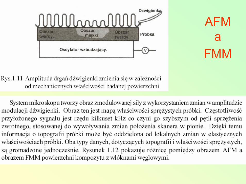
AFM – z modulacją siły (FMM)
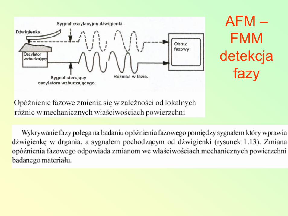
AFM –FMM
detekcja fazy
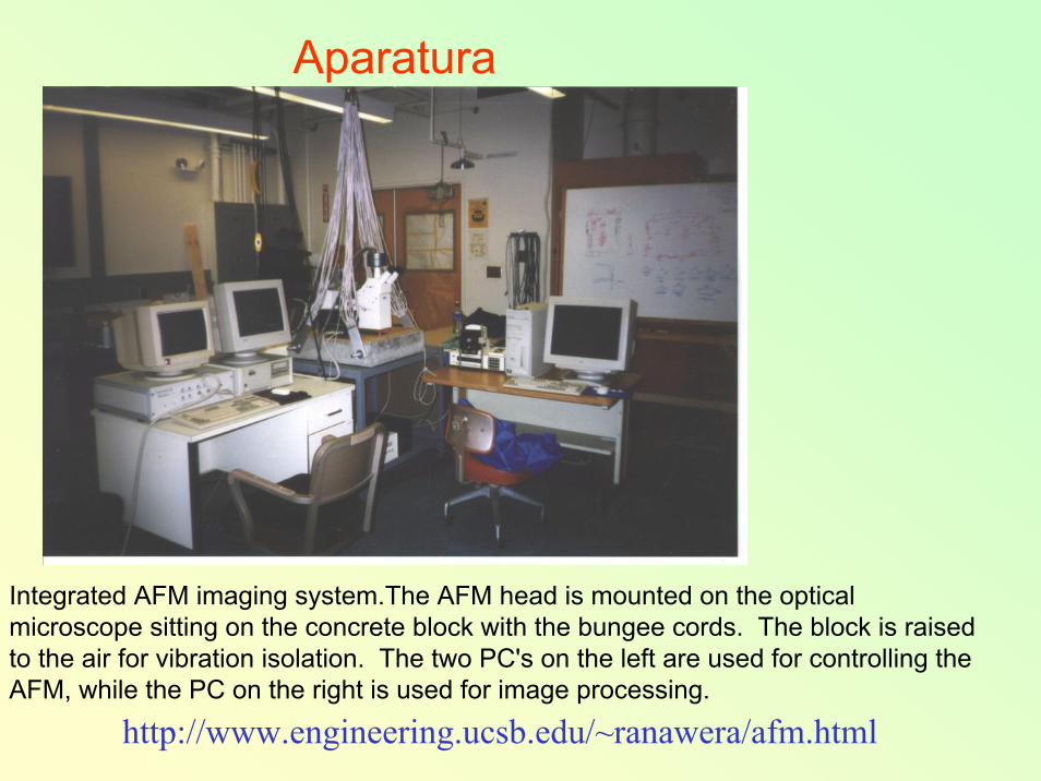
Aparatura
Integrated AFM imaging system.The AFM head is mounted on the optical microscope sitting on the concrete block with the bungee cords. The block is raisedto the air for vibration isolation. The two PC's on the left are used for controlling theAFM, while the PC on the right is used for image processing.
http://www.engineering.ucsb.edu/~ranawera/afm.html
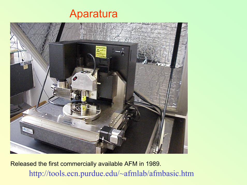
Aparatura
http://tools.ecn.purdue.edu/~afmlab/afmbasic.htmReleased the first commercially available AFM in 1989.

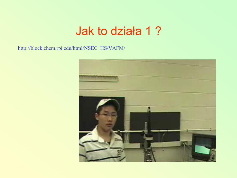
Jak to działa 1 ?http://block.chem.rpi.edu/html/NSEC_HS/VAFM/
Jak to działa 2 ?http://block.chem.rpi.edu/html/NSEC_HS/VAFM/
Jak to działa 3 ?http://block.chem.rpi.edu/html/NSEC_HS/VAFM/
Jak to działa 4 ?http://block.chem.rpi.edu/html/NSEC_HS/VAFM/
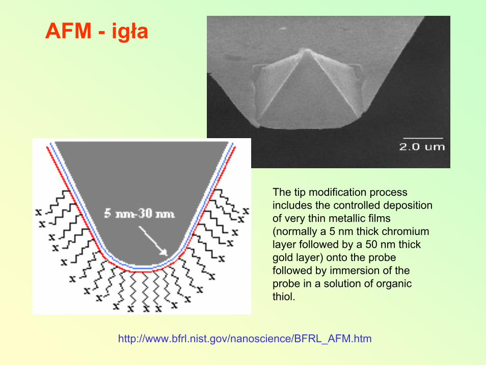
AFM - igła
The tip modification process includes the controlled deposition of very thin metallic films(normally a 5 nm thick chromium layer followed by a 50 nm thick gold layer) onto the probe followed by immersion of the probe in a solution of organic thiol.
http://www.bfrl.nist.gov/nanoscience/BFRL_AFM.htm
AFM -FMM
AFM a
FMM
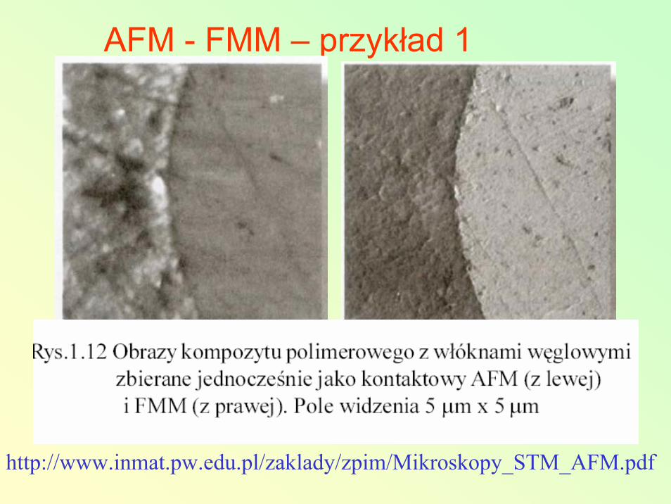
AFM - FMM – przykład 1
http://www.inmat.pw.edu.pl/zaklady/zpim/Mikroskopy_STM_AFM.pdf
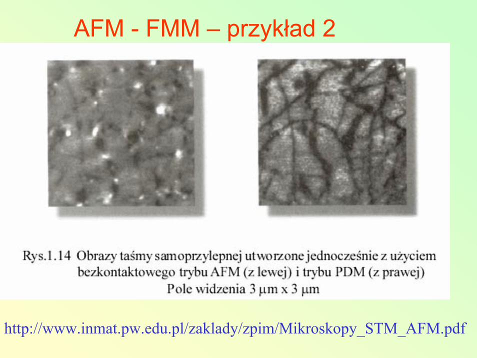
AFM - FMM – przykład 2
http://www.inmat.pw.edu.pl/zaklady/zpim/Mikroskopy_STM_AFM.pdf
Przykłady zastosowania AFM
- metale
- ceramiki
- podzespoły elektroniczne
- układy biologiczne

AFM - metale
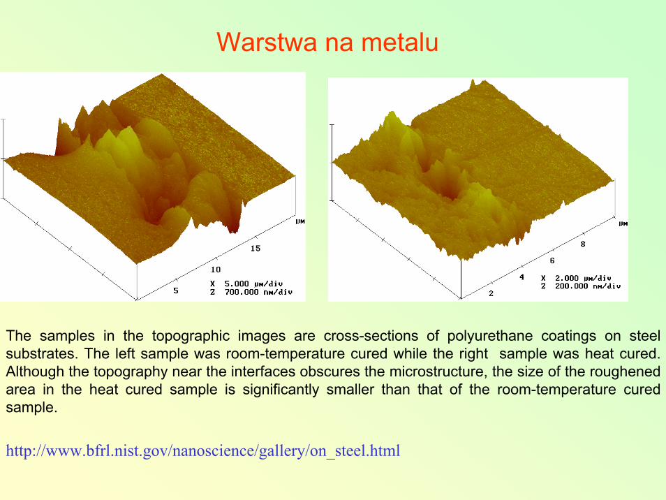
Warstwa na metalu
The samples in the topographic images are cross-sections of polyurethane coatings on steel substrates. The left sample was room-temperature cured while the right sample was heat cured. Although the topography near the interfaces obscures the microstructure, the size of the roughened area in the heat cured sample is significantly smaller than that of the room-temperature cured sample.
http://www.bfrl.nist.gov/nanoscience/gallery/on_steel.html
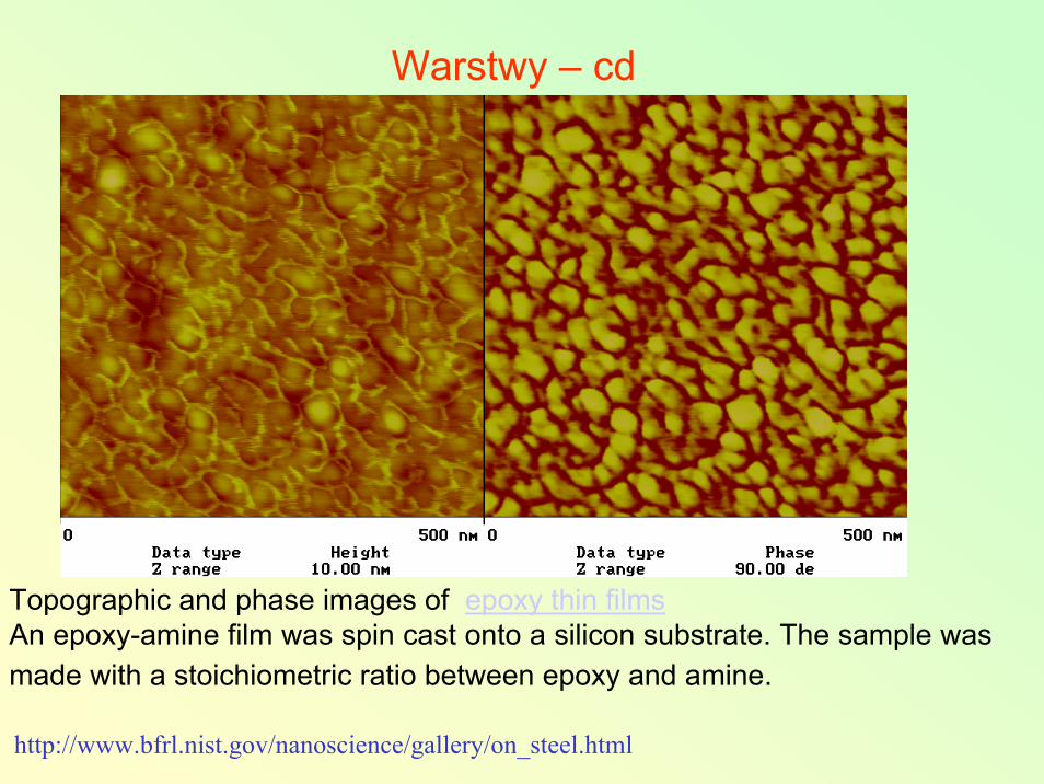
Warstwy – cd
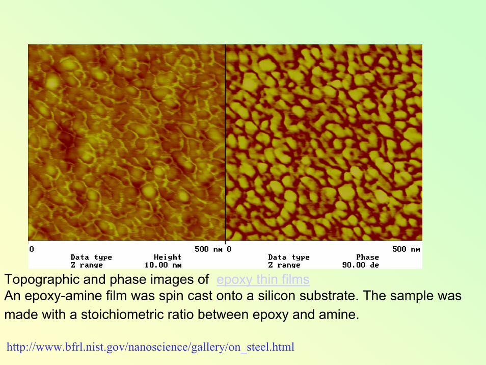
Topographic and phase images of epoxy thin filmsAn epoxy-amine film was spin cast onto a silicon substrate. The sample was made with a stoichiometric ratio between epoxy and amine.
http://www.bfrl.nist.gov/nanoscience/gallery/on_steel.html
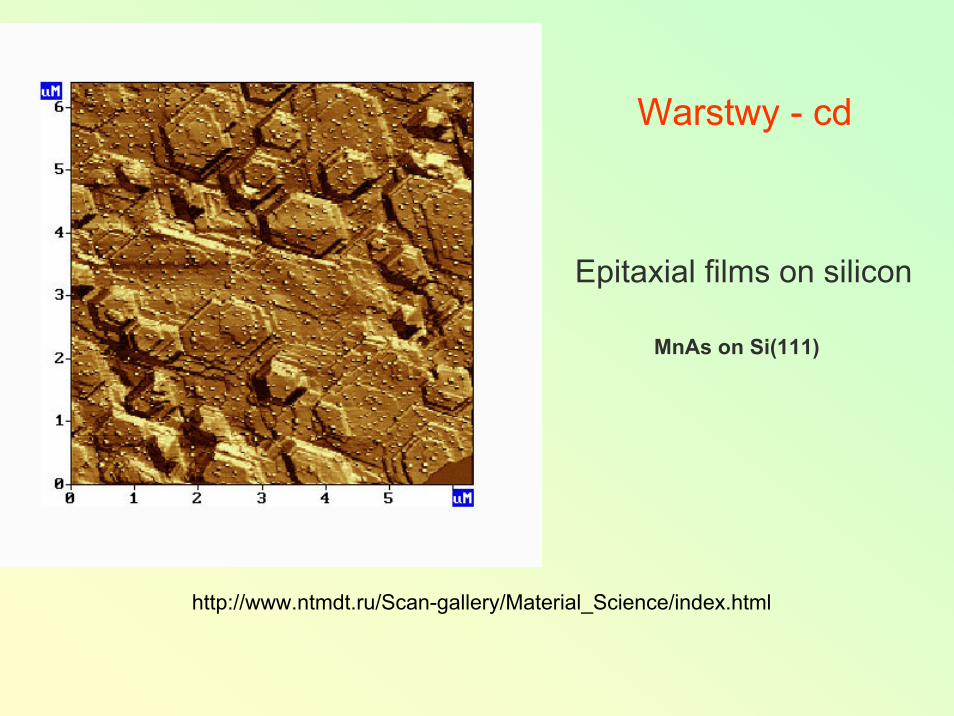
Warstwy - cd
MnAs on Si(111)
Epitaxial films on silicon
http://www.ntmdt.ru/Scan-gallery/Material_Science/index.html
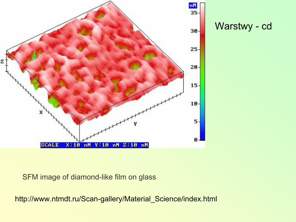
Warstwy - cd
SFM image of diamond-like film on glass.
http://www.ntmdt.ru/Scan-gallery/Material_Science/index.html
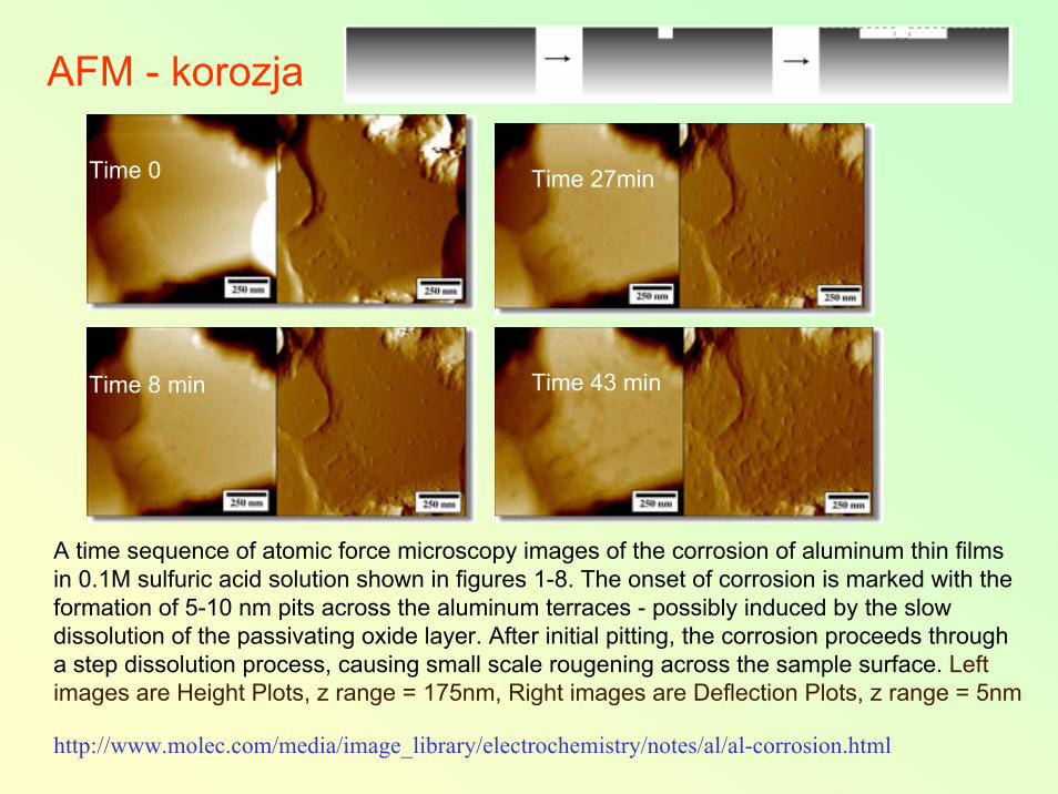
AFM - korozja
http://www.molec.com/media/image_library/electrochemistry/notes/al/al-corrosion.html
A time sequence of atomic force microscopy images of the corrosion of aluminum thin films in 0.1M sulfuric acid solution shown in figures 1-8. The onset of corrosion is marked with the formation of 5-10 nm pits across the aluminum terraces - possibly induced by the slow dissolution of the passivating oxide layer. After initial pitting, the corrosion proceeds througha step dissolution process, causing small scale rougening across the sample surface. Left images are Height Plots, z range = 175nm, Right images are Deflection Plots, z range = 5nm
Time 0
Time 8 min Time 43 min
Time 27min
Topographic and phase images of epoxy thin filmsAn epoxy-amine film was spin cast onto a silicon substrate. The sample was made with a stoichiometric ratio between epoxy and amine.
http://www.bfrl.nist.gov/nanoscience/gallery/on_steel.html
AFM - ceramiki
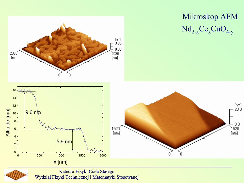
0 500 1000 1500 20000
2
4
6
8
10
12
14
16
9,6 nm
5,9 nm
Altit
ude
[nm
]
x [nm]
Katedra Fizyki Ciała StałegoWydział Fizyki Technicznej i Matematyki Stosowanej
Katedra Fizyki Ciała StałegoWydział Fizyki Technicznej i Matematyki Stosowanej
Nd2-xCexCuO4-y
Mikroskop AFM
0 200 400 600 800 1000 1200 14000
1
2
3
4
5
230 nm
3,6 nmAltit
ude
[nm
]
x [nm]
0 200 400 600 800 1000 1200 14000,0
0,5
1,0
1,5
2,0
640 nm
0,6 nm
1,2 nmAltit
ude
[nm
]
x [nm]
B-B
A-A
Katedra Fizyki Ciała StałegoWydział Fizyki Technicznej i Matematyki Stosowanej
Katedra Fizyki Ciała StałegoWydział Fizyki Technicznej i Matematyki Stosowanej
Nd2-xCexCuO4-y
Mikroskop AFM
h)
Katedra Fizyki Ciała StałegoWydział Fizyki Technicznej i Matematyki Stosowanej
Katedra Fizyki Ciała StałegoWydział Fizyki Technicznej i Matematyki Stosowanej
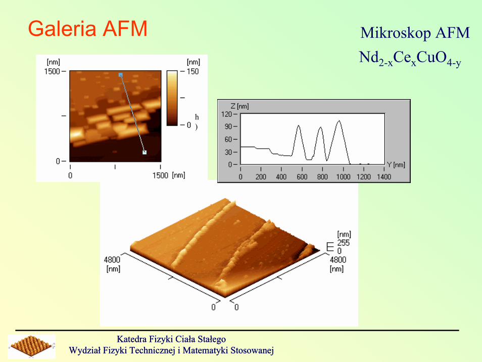
Galeria AFM Mikroskop AFMNd2-xCexCuO4-y
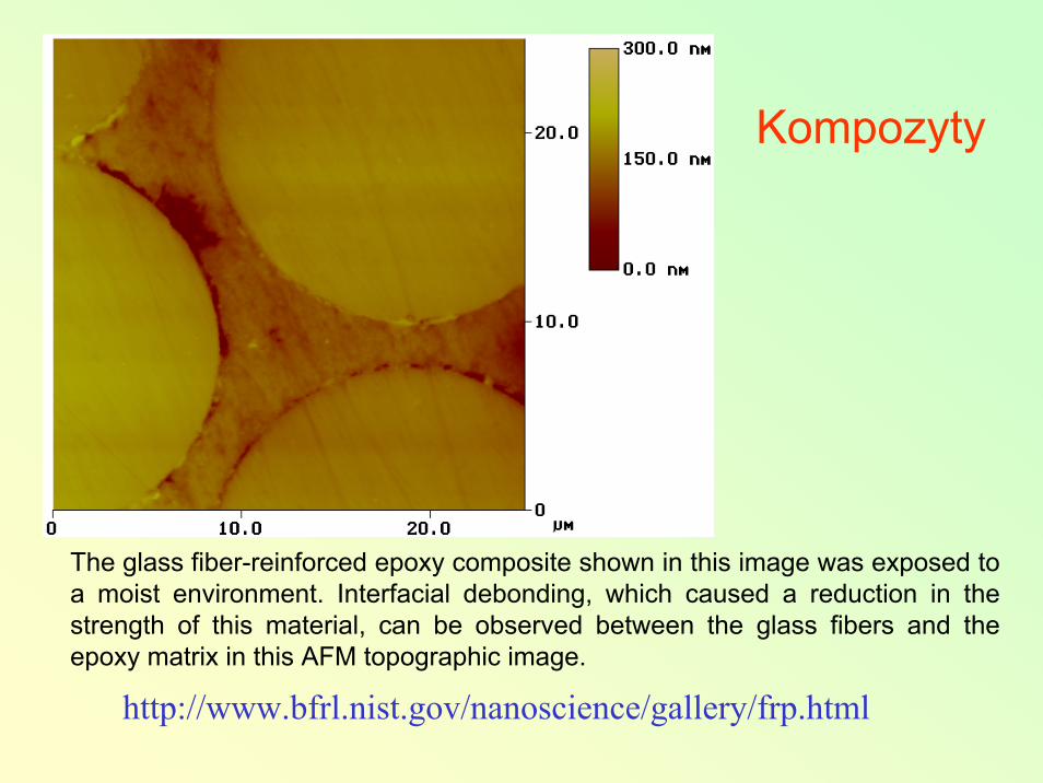
Kompozyty
The glass fiber-reinforced epoxy composite shown in this image was exposed to a moist environment. Interfacial debonding, which caused a reduction in the strength of this material, can be observed between the glass fibers and the epoxy matrix in this AFM topographic image.
http://www.bfrl.nist.gov/nanoscience/gallery/frp.html
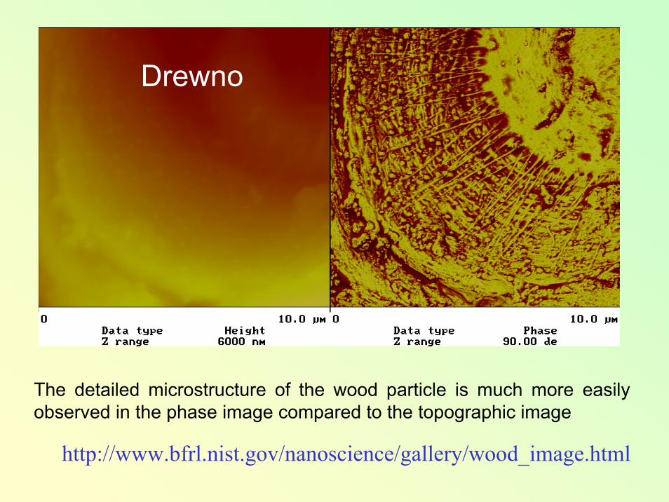
The detailed microstructure of the wood particle is much more easily observed in the phase image compared to the topographic image
http://www.bfrl.nist.gov/nanoscience/gallery/wood_image.html
Drewno
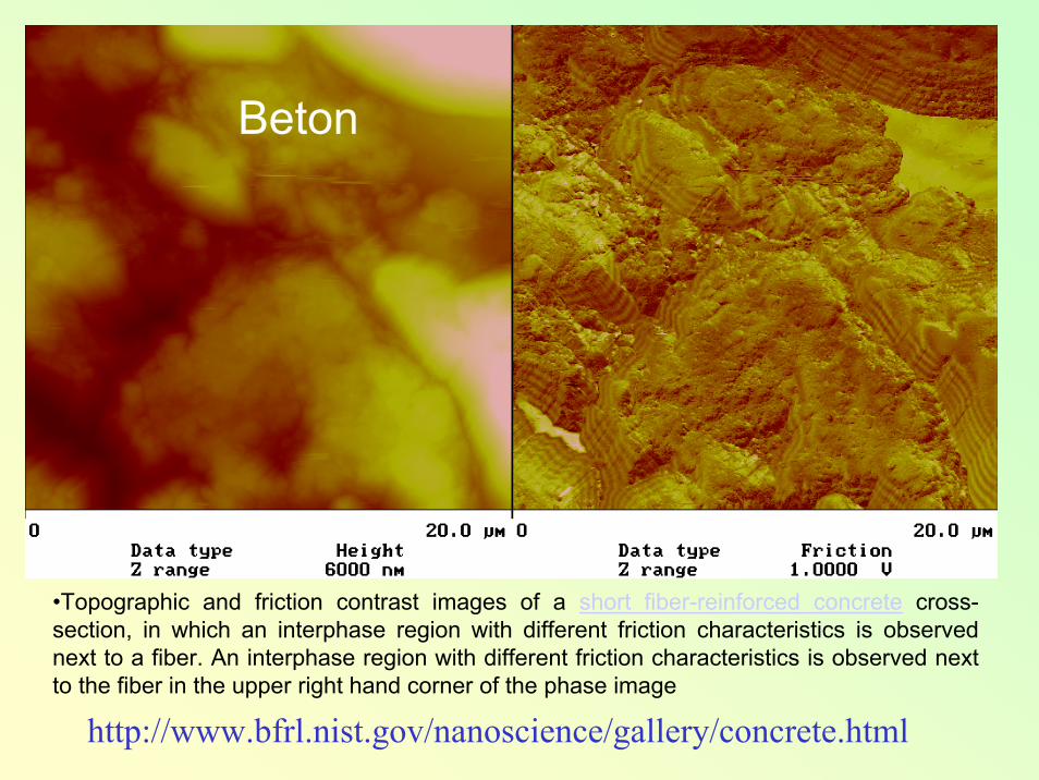
•Topographic and friction contrast images of a short fiber-reinforced concrete cross-section, in which an interphase region with different friction characteristics is observed next to a fiber. An interphase region with different friction characteristics is observed nextto the fiber in the upper right hand corner of the phase image
http://www.bfrl.nist.gov/nanoscience/gallery/concrete.html
Beton
AFM - podzespoły
AFM – podzespoły elektroniczne
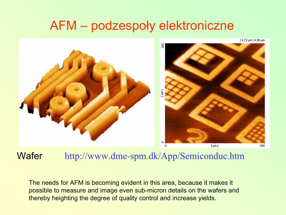
http://www.dme-spm.dk/App/Semiconduc.htmWafer
The needs for AFM is becoming evident in this area, because it makes it possible to measure and image even sub-micron details on the wafers and thereby heighting the degree of quality control and increase yields.
AFM – układy biologiczne
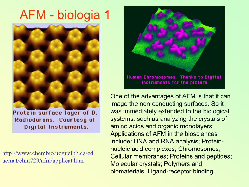
AFM - biologia 1
One of the advantages of AFM is that it can image the non-conducting surfaces. So itwas immediately extended to the biological systems, such as analyzing the crystals ofamino acids and organic monolayers.Applications of AFM in the biosciences include: DNA and RNA analysis; Protein-nucleic acid complexes; Chromosomes;Cellular membranes; Proteins and peptides;Molecular crystals; Polymers and biomaterials; Ligand-receptor binding.
http://www.chembio.uoguelph.ca/educmat/chm729/afm/applicat.htm
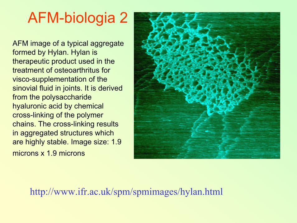
AFM-biologia 2
http://www.ifr.ac.uk/spm/spmimages/hylan.html
AFM image of a typical aggregate formed by Hylan. Hylan is therapeutic product used in the treatment of osteoarthritus forvisco-supplementation of the sinovial fluid in joints. It is derived from the polysaccharide hyaluronic acid by chemical cross-linking of the polymer chains. The cross-linking results in aggregated structures which are highly stable. Image size: 1.9microns x 1.9 microns
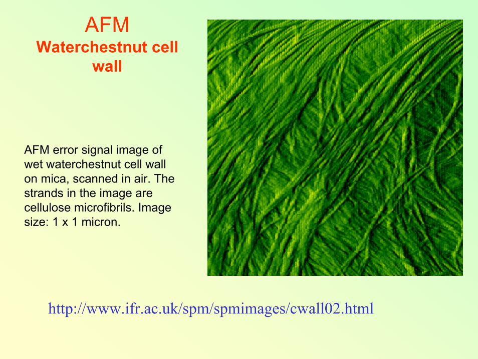
AFMWaterchestnut cell
wall
AFM error signal image ofwet waterchestnut cell wallon mica, scanned in air. The strands in the image are cellulose microfibrils. Image size: 1 x 1 micron.
http://www.ifr.ac.uk/spm/spmimages/cwall02.html
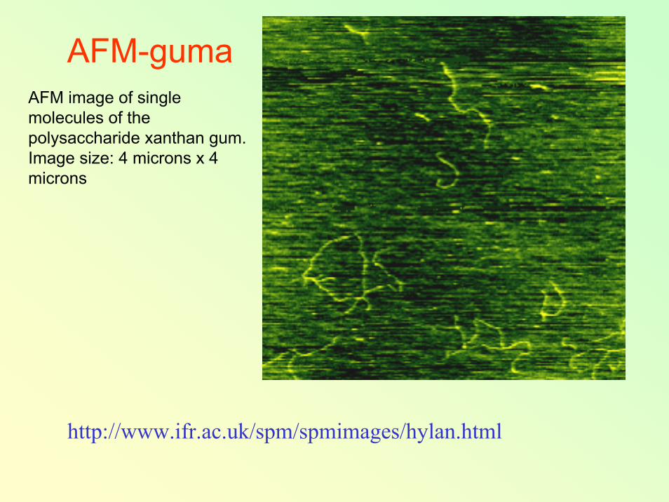
AFM-gumaAFM image of singlemolecules of the polysaccharide xanthan gum.Image size: 4 microns x 4microns
http://www.ifr.ac.uk/spm/spmimages/hylan.html
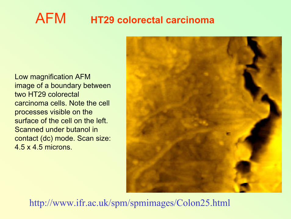
AFM HT29 colorectal carcinoma
Low magnification AFMimage of a boundary between two HT29 colorectal carcinoma cells. Note the cell processes visible on the surface of the cell on the left.Scanned under butanol in contact (dc) mode. Scan size: 4.5 x 4.5 microns.
http://www.ifr.ac.uk/spm/spmimages/Colon25.html
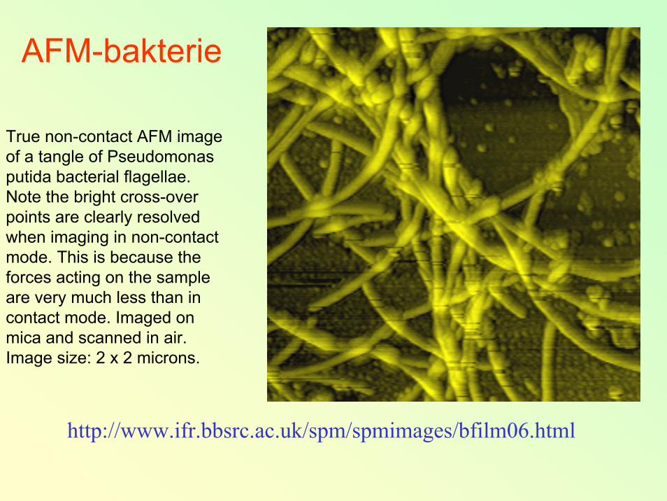
AFM-bakterie
True non-contact AFM image of a tangle of Pseudomonas putida bacterial flagellae.Note the bright cross-over points are clearly resolved when imaging in non-contact mode. This is because the forces acting on the sample are very much less than in contact mode. Imaged onmica and scanned in air.Image size: 2 x 2 microns.
http://www.ifr.bbsrc.ac.uk/spm/spmimages/bfilm06.html
Katedra Fizyki Ciała StałegoWydział Fizyki Technicznej i Matematyki Stosowanej
Katedra Fizyki Ciała StałegoWydział Fizyki Technicznej i Matematyki Stosowanej
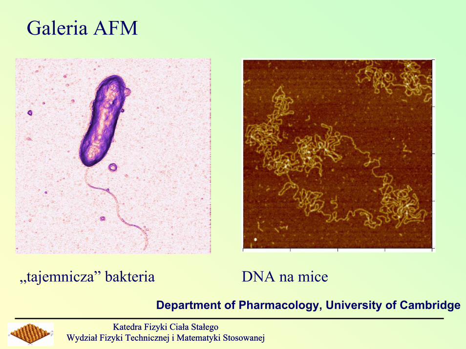
Galeria AFM
„tajemnicza” bakteria DNA na mice
Department of Pharmacology, University of Cambridge
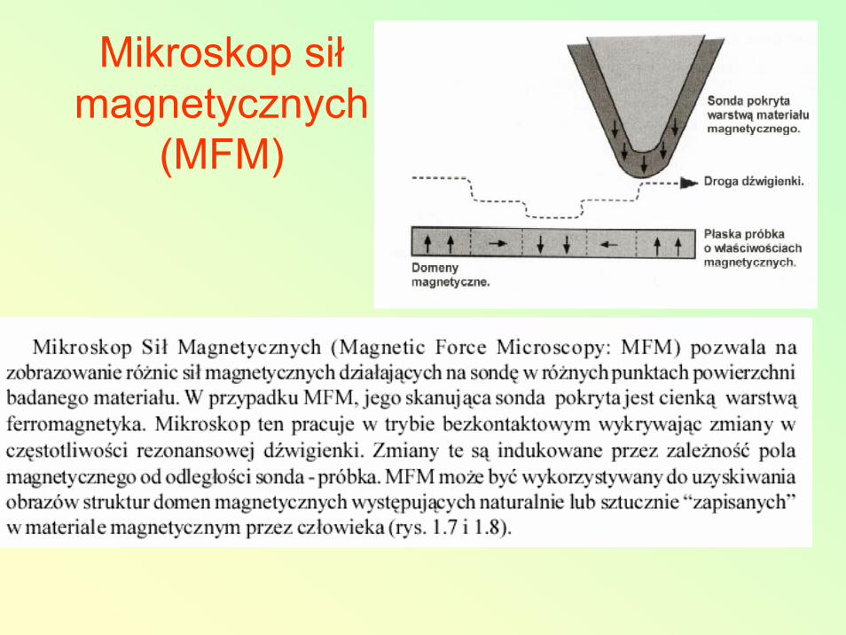
Mikroskop siłmagnetycznych
(MFM)
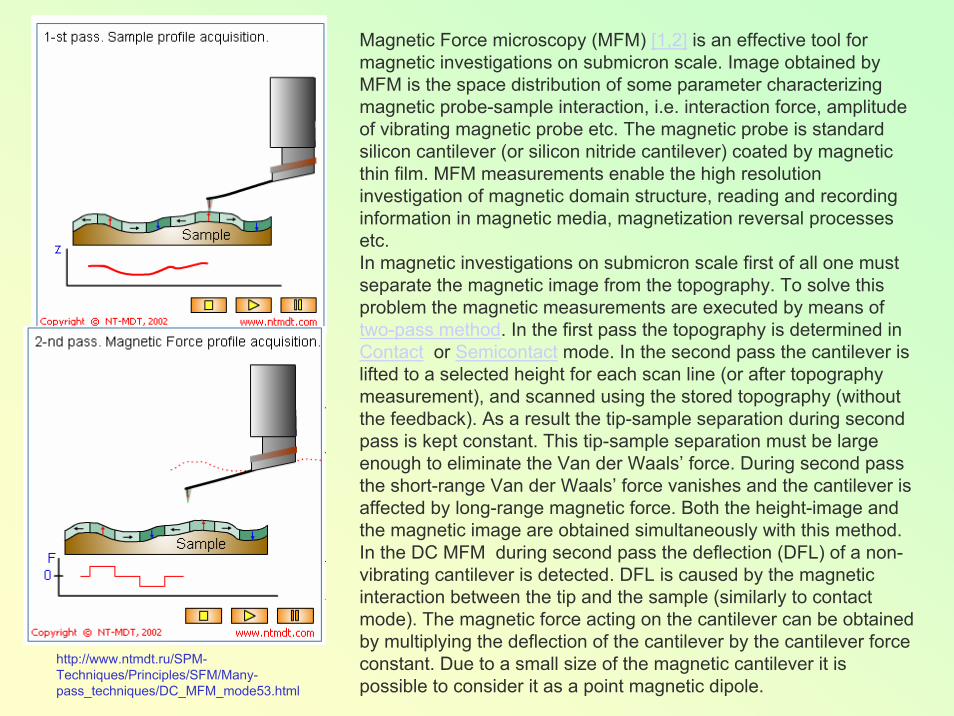
Magnetic Force microscopy (MFM) [1,2] is an effective tool formagnetic investigations on submicron scale. Image obtained by MFM is the space distribution of some parameter characterizing magnetic probe-sample interaction, i.e. interaction force, amplitude of vibrating magnetic probe etc. The magnetic probe is standardsilicon cantilever (or silicon nitride cantilever) coated by magnetic thin film. MFM measurements enable the high resolution investigation of magnetic domain structure, reading and recording information in magnetic media, magnetization reversal processesetc. In magnetic investigations on submicron scale first of all one must separate the magnetic image from the topography. To solve thisproblem the magnetic measurements are executed by means of two-pass method. In the first pass the topography is determined in Contact or Semicontact mode. In the second pass the cantilever is lifted to a selected height for each scan line (or after topography measurement), and scanned using the stored topography (without the feedback). As a result the tip-sample separation during secondpass is kept constant. This tip-sample separation must be large enough to eliminate the Van der Waals’ force. During second passthe short-range Van der Waals’ force vanishes and the cantilever is affected by long-range magnetic force. Both the height-image and the magnetic image are obtained simultaneously with this method.In the DC MFM during second pass the deflection (DFL) of a non-vibrating cantilever is detected. DFL is caused by the magnetic interaction between the tip and the sample (similarly to contact mode). The magnetic force acting on the cantilever can be obtainedby multiplying the deflection of the cantilever by the cantilever force constant. Due to a small size of the magnetic cantilever it is possible to consider it as a point magnetic dipole.
http://www.ntmdt.ru/SPM-Techniques/Principles/SFM/Many-pass_techniques/DC_MFM_mode53.html
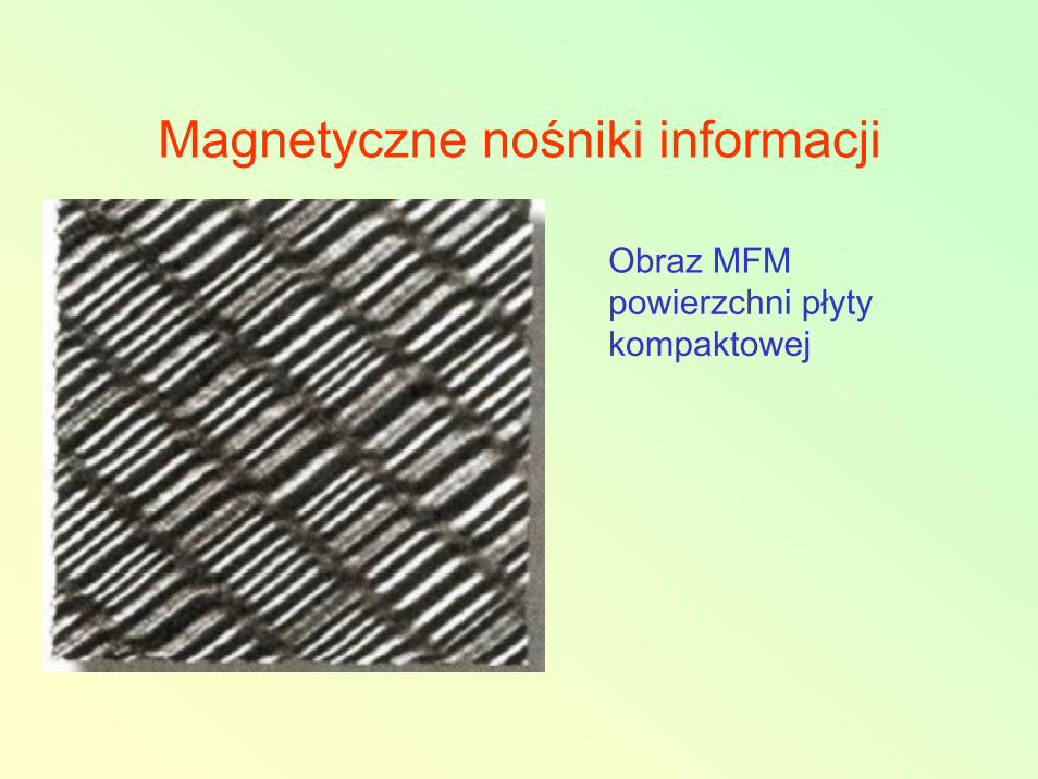
Magnetyczne nośniki informacji
Obraz MFM powierzchni płyty kompaktowej
Katedra Fizyki Ciała StałegoWydział Fizyki Technicznej i Matematyki Stosowanej
Katedra Fizyki Ciała StałegoWydział Fizyki Technicznej i Matematyki Stosowanej
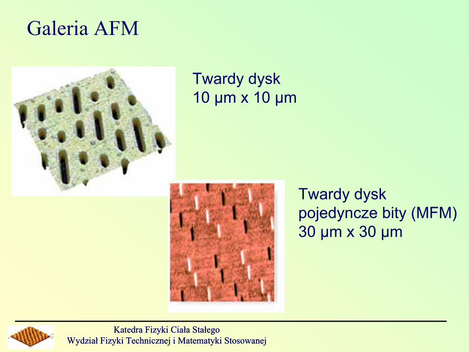
Galeria AFM
Twardy dysk 10 µm x 10 µm
Twardy dyskpojedyncze bity (MFM)30 µm x 30 µm
Metale – topografia i obraz magnetyczny
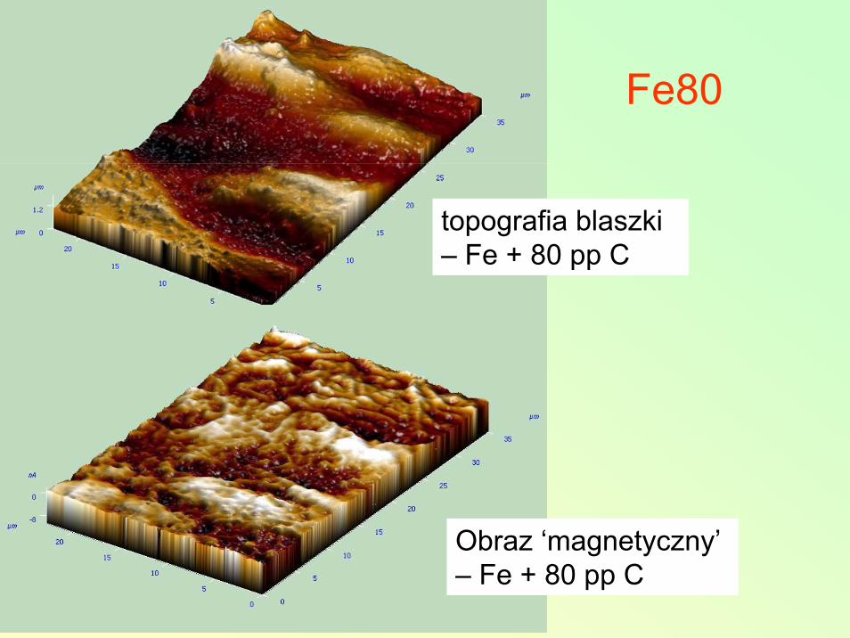
Fe80
topografia blaszki – Fe + 80 pp C
Obraz ‘magnetyczny’– Fe + 80 pp C
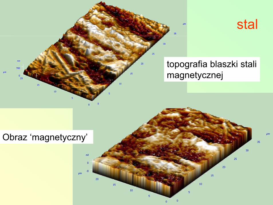
stal
topografia blaszki stali magnetycznej
Obraz ‘magnetyczny’
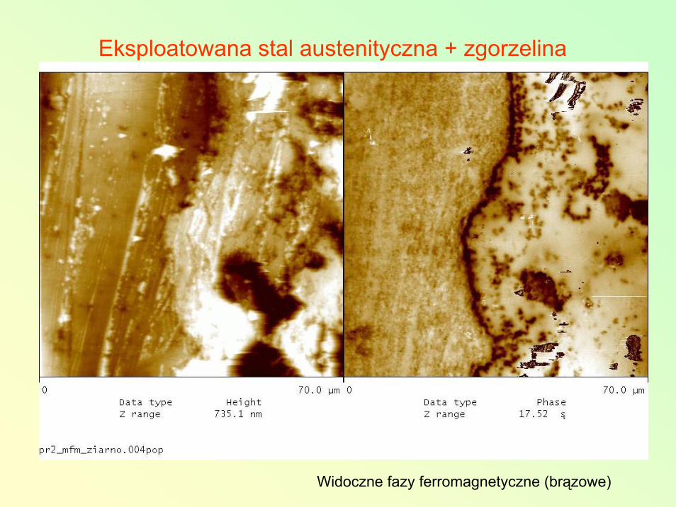
Eksploatowana stal austenityczna + zgorzelina
Widoczne fazy ferromagnetyczne (brązowe)
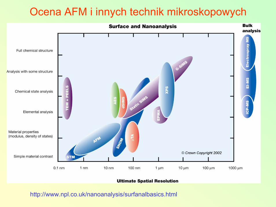
Ocena AFM i innych technik mikroskopowych
http://www.npl.co.uk/nanoanalysis/surfanalbasics.html
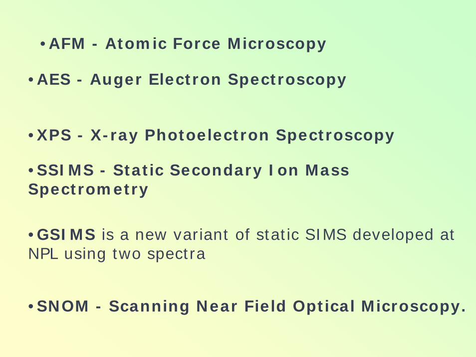
•AES - Auger Electron Spectroscopy
•XPS - X-ray Photoelectron Spectroscopy
•SSIMS - Static Secondary Ion Mass Spectrometry
•GSIMS is a new variant of static SIMS developed atNPL using two spectra
•AFM - Atomic Force Microscopy
•SNOM - Scanning Near Field Optical Microscopy.
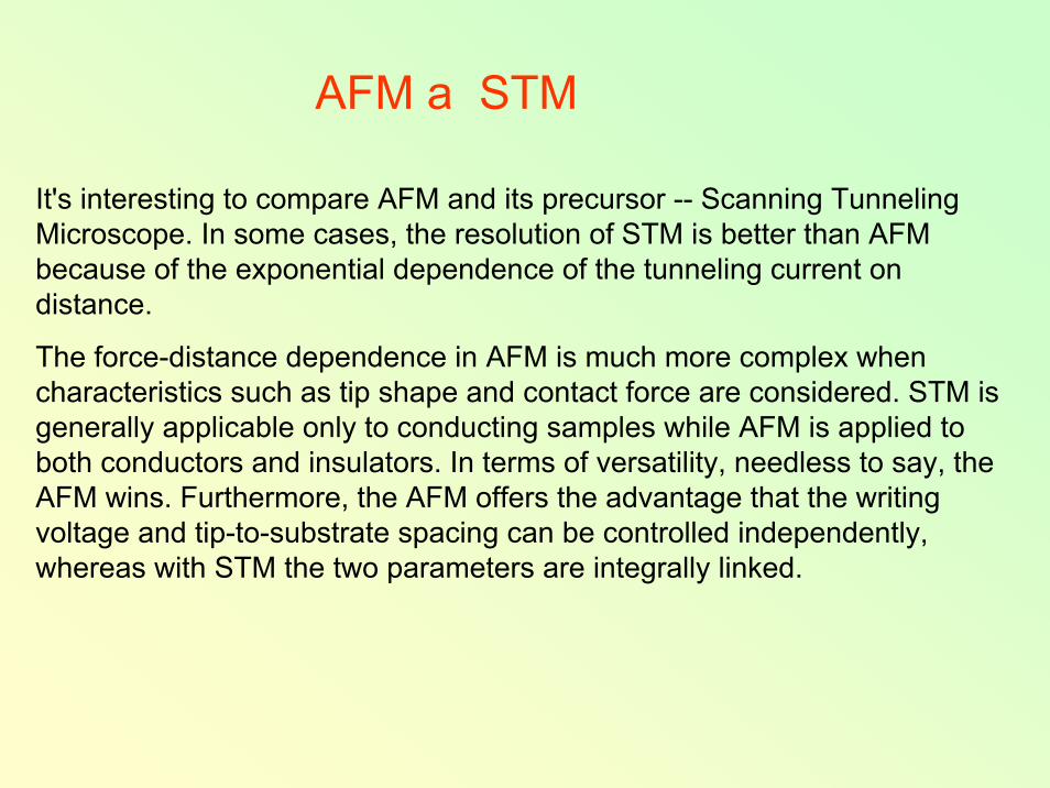
AFM a STM
It's interesting to compare AFM and its precursor -- Scanning Tunneling Microscope. In some cases, the resolution of STM is better than AFMbecause of the exponential dependence of the tunneling current ondistance.
The force-distance dependence in AFM is much more complex when characteristics such as tip shape and contact force are considered. STM is generally applicable only to conducting samples while AFM is applied toboth conductors and insulators. In terms of versatility, needless to say, theAFM wins. Furthermore, the AFM offers the advantage that the writing voltage and tip-to-substrate spacing can be controlled independently,whereas with STM the two parameters are integrally linked.
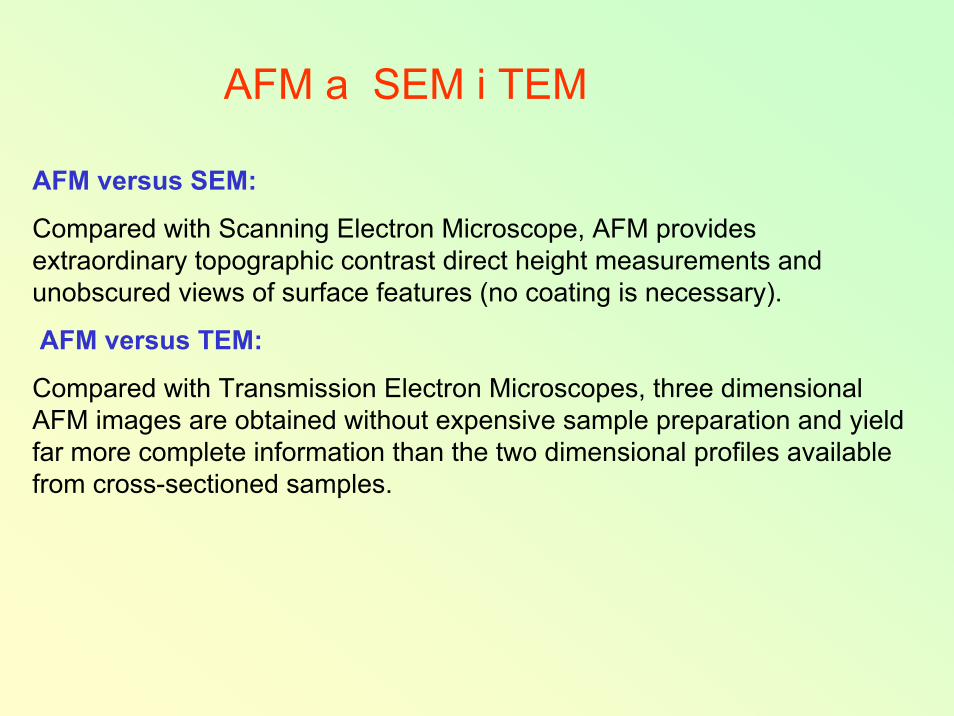
AFM a SEM i TEM
AFM versus SEM:
Compared with Scanning Electron Microscope, AFM provides extraordinary topographic contrast direct height measurements and unobscured views of surface features (no coating is necessary).
AFM versus TEM:
Compared with Transmission Electron Microscopes, three dimensionalAFM images are obtained without expensive sample preparation and yieldfar more complete information than the two dimensional profiles available from cross-sectioned samples.
Suplement

AFM -manipulacja
The AFM is first used in "non-contact" mode toobtain an image of the nanotube by scanning the AFM tip, shown in red in the schematic onthe left, just above the surface.
The AFM tip is then brought down to the surface and is used like a tiny plow to move the nanotube.
Because of the strong interaction between the nanotube and the surface via van der Waals forces, the bent Nanotube stays where it has been placed and maintains its shape, rather than snapping back to its preferred straight configuration.
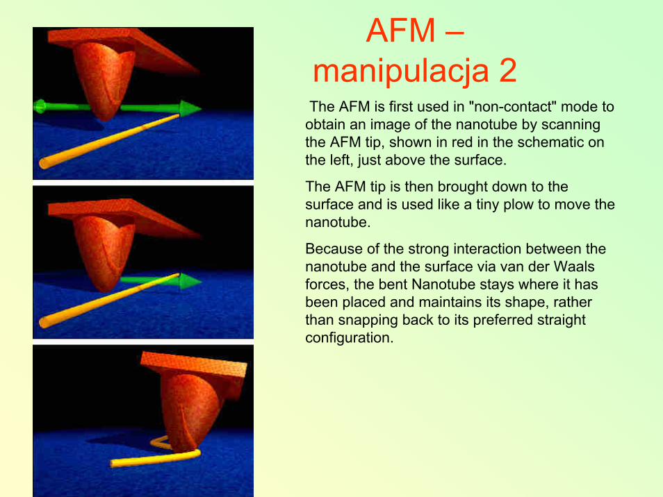
AFM –manipulacja 2The AFM is first used in "non-contact" mode toobtain an image of the nanotube by scanning the AFM tip, shown in red in the schematic onthe left, just above the surface.
The AFM tip is then brought down to the surface and is used like a tiny plow to move the nanotube.
Because of the strong interaction between the nanotube and the surface via van der Waals forces, the bent Nanotube stays where it has been placed and maintains its shape, rather than snapping back to its preferred straight configuration.
AFM –manipulacja 3
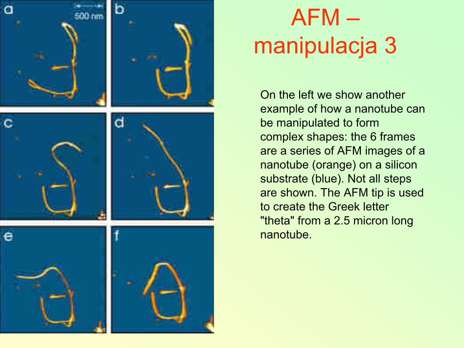
On the left we show anotherexample of how a nanotube canbe manipulated to form complex shapes: the 6 framesare a series of AFM images of a nanotube (orange) on a siliconsubstrate (blue). Not all stepsare shown. The AFM tip is usedto create the Greek letter"theta" from a 2.5 micron longnanotube.


![Dr in . Izabela Barszczewska-Rybarek Politechnika Śą ... · z wykorzystaniem technik obrazowania, takich jak mikroskopia sił atomowych (AFM) [35,38] i skaningowa mikroskopia elektronowa](https://img.pdfslide.tips/doc/110x75/5c76910409d3f231488c40c0/dr-in-izabela-barszczewska-rybarek-politechnika-sa-z-wykorzystaniem.jpg)