Embed Size (px)
Citation preview
M.A. College of Engineering
FFT Processor 1
�
�
��������������
������������������������ ���� ������ ���� ���� ���� ���� ���� ���� ���� �� �������������������������������� ����� �� �� �� �
������������ ������������������������������������ �������������������� ����������������
Guided by Done by Prof. K.Radhakrishnan Ray Ranjan Varghese ELECTRICAL & ELECTRONICS DEPT. Chanjal .G.Tharayil M.A. COLLEGE OF ENGINEERING
���������� � � ������� � � ��������
MMMMaaaar r r r AAAAtttthhhhaaaannnnaaaassssiiiiuuuus s s s CCCCoooolllllllleeeegggge e e e oooof f f f EEEEnnnnggggiiiinnnneeeeeeeerrrriiiinnnngggg ������������������������������������������������
MAHATMA GANDHI UNIVERSITY, KOTTAYAM, KERALA 2001

M.A. College of Engineering
FFT Processor 2
TABLE OF CONTENTS LIST OF FIGURES…………………………………………………… Chapter 1-Introduction to VHDL
1.1 Introduction 1 1.2 Advantages of VHDL over other Hardware… Description Languages……………………………………….. 1 1.3 VHDL : The Language…………………………………… 2 1.3.1 Entity Declaration……………………………….. 3
1.3.2 Architecture Body……………………………….. 3 1.3.3 Configuration Declaration……………………….. 7 1.3.4 Package…………………………………………… 8 1.3.5 Testbench………………………………………… 9
Chapter 2-High Level Design Flow…………………………………. 10 2.1 HDL Capture……………………………………………… 10 2.2 RTL Simulation…………………………………………… 10 2.3 VHDL Synthesis………………………………………….. 12 2.4 Functional Gate Level Verification………………………. 13 2.5 Place and Route…………………………………………... 13 2.6 Post Layout Timing Simulation………………………….. 15 Chapter 3-Illustration of VHDL…………………………………….. 16 3.1 The IEEE floating-point standard………………………… 16 3.2 The Addition Process…………………………………….. 17 3.3 Hardware Implementation of Floating-Point Adder……… 19 3.3.1 Block Diagram of the Adder…………………….. 19 3.3.2 The Subtractor Unit……………………………… 20 3.3.3 The Swap Unit…………………………………… 21 3.3.4 The Shifter Unit………………………………….. 22 3.3.5 The Summer Unit………………………………… 23 3.3.6 The Normalize Unit………………………………. 23 3.3.7 The Control Unit…………………………………. 24 3.3.8 The Testbench for the adder……………………… 28 Chapter 4- The Fourier Transform…………………………………… 30 4.1 The Discrete Fourier Transform…………………………... 30 4.1.1 An Illustration…………………………………….. 30 4.1.2 Types of Fourier Transforms……………………... 31 4.1.3 Notation and Format of the Real DFT……………. 33 4.1.4 DFT Basis Functions……………………………… 34 4.1.5 Analysis, Calculating the DFT……………………. 37
4.2 The Fast Fourier Transform………………………………. 37 4.2.1 Comparison of Real DFT and Complex DFT……. 38 4.2.2 How the FFT works……………………………… 39 4.3 Synthesis, Calculating the Inverse DFT………………….. 42 4.4 Illustration of the DFT and IDFT in Matlab……………… 44 Chapter 5-Architectural Design of the FFT Processor……………… 46 5.1 Block Diagram of the FFT Processor…………………….. 46

M.A. College of Engineering
FFT Processor 3
5.2 Butterfly Processing Element…………………………….. 48 5.3 Address Generation Unit…………………………………. 50 5.3.1 Butterfly Generator……………………………… 52 5.3.2 Stage Generator………………………………….. 52 5.3.3 Stage Done_IO Done Block……………………... 52 5.3.4 IO-Address Generator…………………………… 53 5.3.5 Base Index Generator……………………………. 53 5.3.6 The Shifters……………………………………… 54 5.3.7 ROM Address Generator………………………... 54 5.4 Controller…………………………………………………. 55 5.5 RAM and ROM…………………………………………... 55 Chapter 6-RTL Simulation of the FFT Processor…………………... 56 Chapter 7-Synthesis of the FFT Processor………………………….59 Chapter 8-Conclusion………………………………………………. 60 APPENDIX A-Code Listing……………………………………….. 61 APPENDIX B-Synthesis Results…………………………………... 101
References ………………………………………………………….112

M.A. College of Engineering
FFT Processor 4
LIST OF FIGURES Figure 1.1 – Half Adder…………………………………………… 3 Figure 2.1 – High Level Design Flow…………………………….. 11 Figure 3.1 – IEEE Format of Floating Point Numbers……………. 16 Figure 3.2 – Block Diagram of the Floating Point Adder Unit…… 20 Figure 3.3 – Structure of a Finite State Machine…………………. 25 Figure 4.1 – Sampled Values of signal being decomposed………. 29 Figure 4.2 – Sine and Cosine Waves after Fourier Decomposition. 30 Figure 4.3 – Types of Fourier Transforms………………………... 32 Figure 4.4 – DFT Terminology…………………………………… 33 Figure 4.5 – DFT Basis Functions………………………………… 36 Figure 4.6 – Comparison of Real and Complex DFT…………….. 38 Figure 4.7 – Signal Flow Graph for 8-point DIT-FFT with Input Scrambling…………………………………………………. 40 Figure 4.8 – Signal Flow Graph for 8-point modified DIT-FFT With Output Scrambling………………………………………….. 41 Figure 4.9 – The Bandwidth of Frequency Domain Signals……... 44 Figure 5.1 – FFT Computation Process…………………………... 46 Figure 5.2 – Block Diagram of FFT Processor…………………... 47 Figure 5.3 – Butterfly Processing Unit…………………………... 48 Figure 5.4 – Waveform of the Cycles used in the FFT Processor.. 49 Figure 5.5 – Address Generation Unit…………………………… 51

M.A. College of Engineering
FFT Processor 5
CHAPTER 1
INTRODUCTION TO VHDL
1.1 Introduction
VHDL is an acronym for VHSIC Hardware Description language
(VHSIC stands for Very High Speed Integrated Circuits ). It is a
hardware description language that can be used to model a digital
system at many levels of abstraction ranging from the algorithmic level
to the gate level. The complexity of the digital system being modeled
could vary from that of a simple gate to a complete digital electronic
system, or anything in between.
VHDL can be regarded as an integrated amalgamation of the
following languages : sequential + concurrent + netlist + timing
specification + waveform generation language.
Therefore the language has constructs that enable to express the
concurrent or sequential behavior of a digital system with or without
timing. It also allows modeling the system as an interconnection of
components. Test waveforms can also be generated using the same
constructs. All the above constructs can be combined to provide a
comprehensive description of the system in a single model.
1.2 Advantages of VHDL over other hardware description
languages.
1. The language con be used as a communication medium
between different CAD and CAE tools.
2. The language supports hierarchy; that is, a digital system can
be modeled as a set of interconnected components each
component in turn can be modeled as a set of interconnected
subcomponents.

M.A. College of Engineering
FFT Processor 6
3. The language supports flexible design methodologies top-
down, bottom-up or mixed.
4. It supports both synchronous and asynchronous timing models.
5. Various digital modeling techniques such as finite state
machine descriptions, algorithmic descriptions and Boolean
equations can be modeled using this language.
6. The language is publicly available, human readable, machine
readable and not proprietary.
7. The language supports three basic different description styles:
structural, dataflow and behavioral.
8. Arbitrarily large designs can be modeled using the language
and therefore there are no limitations imposed by the language
on the size of a design.
9. The model can not only describe the functionality of a design,
but also contain information about the design itself in terms of
user-defined attributes, such as total area and speed.
10. The capability of defining new data types provides the power
to describe and simulate a new design technology at a very
high level of abstraction without any concern about the
implementation details.
1.3 VHDL : The language.
VHDL is a hardware description language that can be used to
model a digital system. The digital system con be as simple as a logic
gate or as complex as a complete electronic system. The building blocks
of this language are called as design units. The four main design units
are:
1. Entity declaration.
2. Architecture declaration.
M.A. College of Engineering
FFT Processor 7
3. Configuration declaration.
4. Package.
The design units are described below.
1.3.1 Entity declaration.
An entity is modeled using an entity declaration and at least one
architecture body. The entity declaration describes the external view of
an entity. The entity declaration specifies the name of the entity being
modeled and lists the set of interface ports. Ports are signals (wires)
through which the entity communicates with the other models in its
external environment. An example for a half-adder circuit is given
below.
Figure 1.1 : Half Adder
entity HALF-ADDER is
port ( A,B : in BIT; SUM, CARRY : out BIT );
end HALF-ADDER;
This entity called HALF-ADDER has two input ports A and B ; and two
output ports SUM and CARRY .Bit is a predefined type of language
construct.
1.3.2 Architecture body.
The second important part of a VHDL source file is the architecture
declaration. Every entity declaration you write must be accompanied by
at least one corresponding architecture. An architecture declaration is a

M.A. College of Engineering
FFT Processor 8
statement that describes the underlying function and/or structure of a
circuit. Each architecture in your design must be associated by name
with one entity in the design. The architecture body contains the
internal description of the entity. The internal structure can be specified
by any of the following modeling styles.
a) As a set of interconnected components.
b) As a set of concurrent assignment statements.
c) As a set of sequential assignment statements.
d) As a combination of the above three.
The different modeling styles are explained below.
a. Structural style of modeling.
This is modeled as a set of interconnected components. Such a
model for a HALF-ADDER is shown.
architecture HA-STRUCTURE of HALF-ADDER is
component XOR2
port ( X,Y: in BIT ; N: out BIT )
end component;
component AND2
port ( L,M : in BIT; N: out BIT);
end component;
begin
X1: XOR2 port map (A,B,SUM);
A1: AND2 port map (A,B, CARRY);
end HA-STRUCTURE ;
The name of the architecture body is HA-STRUCTURE. The
architecture body is composed of two parts : the declarative part (before
M.A. College of Engineering
FFT Processor 9
the keyword begin ) and the statement part ( after keyword begin). Two
component declarations are present in the declarative part of the
architecture body.
The declared components are instantiated in the statement part of
the architecture body using component instantiation statements. X1 and
A1 are the component labels for these component instantiations. The
first component instantiation statement labeled X1, shows that signals A
and B are connected to output port SUM of the HALF-ADDER entity.
Similarly in the second component instantiation statement, signals A
and B are connected to ports L and M of the AND2 component, while
port N is connected to the CARRY-PORT of the HALF-ADDER.
b. Data flow style of modeling.
In this modeling style, the flow of data through the entity is expressed
primarily using concurrent signal assignment statements. The structure
of the entity is not explicitly specified in this modeling style, but it can
be implicitly deduced. The data flow model of the HALF-ADDER
entity is given below.
architecture DATAFLOW of HALF-ADDER is
begin
SUM <= A xor B after 8ns;
CARRY <= A and B after 4ns;
end DATAFLOW;
The dataflow is described using two concurrent signal assignment
statements (or sequential signal assignment statements ). In a signal
assignment statement, the symbol <= implies an assignment of a value
to a signal. The value of the expression on the right hand side of the
statement is computed and is assigned to the signal on the lef t-hand side,
M.A. College of Engineering
FFT Processor 10
called the target signal. A concurrent signal assignment statement is
executed only when any signal used in the expression on the right hand
side has an event on it, that is the value for the signal changes. Delay
information is also included in the signal assignment statements using
‘after’ clauses.
c. Behavioral style of modeling
The behavioral style of modeling specifies the behavior of an
entity as a set of statements that are executed sequentially in the
specified process statement. They do not explicitly specify the structure
of the entity but merely its functionality . A process statement is a
concurrent statement that can appear within an architecture body. For
example, consider the following behavioral model for the same HALF-
ADDER.
architecture BEHAVIOR of HALF-ADDER is
begin
process ( A,B )
variable X,Y: BIT;
begin
X:=A ;
Y:=B ;
SUM <= X xor Y;
CARRY <= X and Y;
end process;
end BEHAVIOR;
A process statement also has a declarative part (before keyword
begin) and a statement part ( between keyword begin and end process ).
The statements appearing within the statement part are executed

M.A. College of Engineering
FFT Processor 11
sequentially. The list of signals specified within the parentheses after the
keyword process constitutes a sensitivity list and the process statement
is invoked whenever there is and event on any signal in the list. In the
example when an event occurs on A of B the statements appearing
within the process statement are executed sequentially. However, all the
processes that appear in a design are executed concurrently.
The variable declaration ( starts with the keyword variable )
declares two variables X and Y. A variable is different from a signal in
that it is always assigned a value instantaneously and the assignment
operator used is := compound symbol; contrast this with a signal that is
assigned a value always after a certain delay and the assignment
operator used to assign a value to a signal is the <= compound signal.
Variables declared within a process have their scope limited to that
process. Signal assignment statements appearing within a process are
called sequential signal assignment statements. Sequential signal
assignment statements, including variable assignment statements, are
executed sequentially independent of whether an event occurs on any
signals in its right-hand side expression.
d. Mixed style of modeling
It is possible to mix the three modeling styles which were
described before in a single architecture body. That is, within an
architecture body, we could use component instantiation statements and
concurrent statements, therefore their order of appearance within the
architecture body is not important. Note that a process statement itself is
a concurrent statement; however statements within a process statement
art always executed sequentially.
1.3.3 Configuration declaration
A configuration declaration is used to select one of the possibly
many architecture bodies that an entity may have, and to bind
M.A. College of Engineering
FFT Processor 12
component instances to entities. For structural models, configurations
can be thought of as the parts list for the model. For component
instances, the configuration specifies from many architectures for an
entity, which architecture to use for a specific instance. When the
configuration for an entity-architecture combination is compiled into the
library, a simulatable object is created. An example of the configuration
declaration for the HALF-ADDER entity is given below.
library CMOS-LIB, MY-LIB;
configuration CONFIG of HALF-ADDER is
for HA-STRUCTURE
for X1: XOR2
use entity CMOS-LIB.XOR-GATE (DATAFLOW);
end for ;
for A1 : AND2
use configuration MY-LIB.AND-CONFIG;
end for;
end for;
end CONFIG;
1.3.4 Package
The primary purpose of a package is to encapsulate elements that can be
shared (globally) among two or more design units. A package is a
common storage area used to hold data to be shared among a number of
entities. Declaring data inside of a package allows the data to be
referenced by other entities; thus, the data can be shared.
A package consists of two parts: a package declaration section and a
package body. The package declaration defines the interface for the
package, much the same way that the entity defines the interface for a
model. The package body specifies the actual behavior of the package in
the same method that the architecture statement does for a model.
M.A. College of Engineering
FFT Processor 13
1.3.5 Testbench
A testbench is used to verify the functionality of a design. The testbench
allows the designer to verify the functionality of the design at each step
in the HDL synthesis-based methodology. When the designer makes a
small change to fix an error, the change can be tested to make sure that it
did not affect other parts of the design. New versions of the design can
be verified against known good results to verify compatibility.
A testbench is at the highest level in the hierarchy of the design. The
testbench instantiates the design under test (DUT). It provides the
necessary input stimulus to the DUT and examines the output from the
DUT.

M.A. College of Engineering
FFT Processor 14
CHAPTER 2
HIGH LEVEL DESIGN FLOW
The high level design flow is illustrated in figure 2.1. Each step is
explained below.
2.1 HDL Capture
After the specification has been completed, the designer can begin the
process of implementation. The designer creates the VHDL description
that describes the clock-by-clock behaviour of the design. The VHDL
code for entities of the design are entered. The designer then checks the
design for any syntax errors. After all syntax errors are removed, the
VHDL code is verified for correctness by simulating it.
2.2 RTL Simulation
In RTL Simulation, the designer uses stimulus that represents the design
environment to drive the design and check to make sure that the results
are correct. A standard VHDL simulator can be used to read the RTL
VHDL description and verify the correctness of the design.
The VHDL simulator reads the VHDL description, compiles it into an
internal format, and then executes the compiled format using test
vectors. The designer can look at the output of the simulation and
determine whether or not the design is working properly. The designer
has a number of ways to analyze the output. The most common are
waveform output and tabular output.

M.A. College of Engineering
FFT Processor 15
Design Specif icat ion
Place and Route
HDL Capture
Funct ional GateSimulation
RTL Simulat ion
RTL Synthesis
Post LayoutTiming Simulation
Figure 2.1 High Level Design Flow
M.A. College of Engineering
FFT Processor 16
2.3 VHDL Synthesis
The goal of the VHDL Synthesis step is to create a design that
implements the required functionality and matches the designer’s
constraints in speed, area, or power.
The VHDL synthesis tools convert the VHDL description into a netlist
in the target FPGA or ASIC technology. For the VHDL synthesis tool to
perform this step properly, the VHDL code must be written in a
particular style.
The designer reads the VHDL design into the VHDL synthesis tool. The
tool reports syntax errors and synthesis errors. Synthesis errors usually
result from the designer using constructs that are not synthesisable. In
such cases, the code has to be modified and simulated again.
The synthesiser produces an output netlist in the target technology and a
number of report files. The designer looks at the report files to
determine the quality of the synthesis output. The most common output
files are the timing report and the area report. Most synthesis tools
produce a number of other reports such as hierarchy reports, instance
reports, net reports, power reports, and others. The most useful reports
initially are the timing and area reports, because these are usually the
most critical factors.
The area report shows the designer how much of the resources of the
chip the design has consumed. The designer can tell if the design is too
big for a particular chip and the designer needs to target a larger chip, if
the design should go into a smaller chip, or if the current chip will work
fine. The designer can also get a relative size of the design to use in later
stages of the design process.
The timing report shows the timing of critical paths or specified paths of
the design. The designer examines the timing of the critical paths closely
because these paths ultimately determine how fast the design can run. If

M.A. College of Engineering
FFT Processor 17
the longest path is a timing critical part of the design and is not meeting
the speed requirements of the designer, then the designer may have to
modify the VHDL code or try new timing constraints to make the path
meet timing.
The most important type of output data is the netlist for the design in the
target technology. This output is a gate or macro level output in a format
compatible with the place and route tools that are used to implement the
design in the target chip. For instance, most place and route tools for
FPGA technologies take in an EDIF netlist as an input format. The
primitives used in the netlist are those used in the synthesis library to
describe the technology. The place and route tools understand what to
do with these primitives in terms of how to place a primitive and how to
route wires to them.
2.4 Functional Gate Level Verification
Some designers might want to do a quick check on the output of the
synthesis tool to make sure that the synthesis tool produced a design that
is functionally correct. To do this the designer runs a functional gate
level verification. The designer reads the output VHDL netlist from the
synthesis tool plus a library of the synthesis primitives into the VHDL
simulator and runs the simulation using the RTL Verification vectors. If
the design matches, then the synthesis tool did not produce logic
mismatches; if it does not match, the designer needs to debug the VHDL
RTL description to see what is wrong.
2.5 Place and Route
Place and route tools are used to take the design netlist and implement
the design in the target technology device. The place and route tools
place each primitive from the netlist into an appropriate location on the

M.A. College of Engineering
FFT Processor 18
target device and then route signals between the primitives to connect
the devices according to the netlist.
One input to the place and route tools is the netlist in EDIF or another
netlist format. Another input to some place and route tools is the timing
constraints, which give the place and route tools an indication about
which signals have critical timing associated with them and to route
these nets in the most timing efficient manner. These nets are typically
identified during the static timing analysis process during synthesis.
These constraints tell the place and route tool to place the primitives in
close proximity to one another and to use the fastest routing. The closer
the cells are, the shorter the routed signals will be and the shorter the
time delay.
Some place and route tools allow the designer to specify the placement
of large parts of the design. This process is also known as floor
planning. Floor planning allows the user to pick locations on the chip for
large blocks of the design so that routing wires are as short as possible.
The designer lays out blocks on the chip as general areas. The floor
planner feeds this information to the place and route tools so that these
blocks are placed properly. After the cells are placed, the router makes
the appropriate connections.
After all the cells are place and routed, the output of the place and route
tools consists of data files that can be used to implement the chip. In the
case of FPGAs, these files describe all of the connections needed to fuse
FPGAs macrocells to implement the functionality required. Anti-fuse
FPGAa use this information to burn the appropriate fuses while
reprogrammable devices download this information to the device to turn
on the appropriate transistor connections.
The other output from the place and route software is a file used to
generate the timing file. This file describes the actual timing of the

M.A. College of Engineering
FFT Processor 19
programmed FPGA device or the final ASIC device. This timing file, as
much as possible, describes the timing extracted from the device when it
is plugged into the system for testing. The most common format of this
file for most simulators is the SDF(Standard Delay Format).
2.6 Post Layout Timing Simulation After the place and route process has completed, the designer will want
to verify the results of the place and route process. There are a number
of methods to accomplish this task but the most common is to use post
route gate level simulation. This simulation combines the netlist used for
place and route with the timing file from the place and route process into
a simulation that checks both functionality and timing of the design. The
designer can run the simulation and generate accurate output waveforms
that show whether or not the device is operating properly and if the
timing is being met. For VHDL simulations this requires a VITAL-
compliant (standard way of describing designs with designs that allow
SDF timing back annotation) VHDL Simulator.

M.A. College of Engineering
FFT Processor 20
CHAPTER 3
ILLUSTRATION OF VHDL
VHDL is illustrated below using an example of a floating point adder
unit which forms a part of the processor.
3.1 The IEEE Floating-Point Standard
The IEEE computer society has developed a standard for binary
floating-point arithmetic. The basic format sizes are 32 bits (single
precision) and 64 bits (double precision). The 32 bit format is used in
this project. As shown in figure, the 32 bits used in single precision are
divide into three separate groups : bits 0 through 22 form the mantissa,
bits 23 through 30 form the exponent, and bit 31 is the sign bit.
31 30 23 22 0
sign exponent Mantissa
Figure 3.1 IEEE format of floating point numbers
These bits form the floating point number, V , by the following relation:
V = (-1)s
* M * 2E – 127
The term : (-1)s
, simply means that the sign bit, S, is 0 for a positive
number and 1 for a negative number. The variable, E, is the number
between 0 and 255 represented by the eight exponent bits. Subtracting
127 from this number allows the exponent term to run from 2-127 to 2128 .
In other words, the exponent is stored in offset binary with an offset of
127.
The mantissa, M, is formed from the 23 bits as a binary fraction. For
example, the binary fraction: 1.0101, means: 1 + 0/2 + ¼ + 0/8 + 1/16.

M.A. College of Engineering
FFT Processor 21
Floating point numbers are normalized in the same way as scientific
notation, that is there is only one nonzero digit left of the decimal point
(called a binary point in base 2). Since the only nonzero number that
exists in base two is 1, the leading digit in the mantissa will always be a
1, and therefore does not need to be stored. The 23 stored bits, referred
to by the notation: m22, m21, ………………., m0, form the mantissa according
to:
M= 1.m22m21m20 ………….. m0.
In other words, M=1 + m22 * 2-1 + m21 * 2
-2 + m20 * 2-3 + ……
Zero is treated as a special number. For zero, the exponent and mantissa
bits are all zeroes. The sign bit could be ‘1’ or ‘0’.
3.2 The Addition Process
The steps involved in the addition/subtraction process are the following :
1. Choose the number with the smaller exponent.
2. Concatenate the implied ‘1’ bit with the mantissa of this number
and shift it to the right by a number of steps equal to the
difference in exponents.
3. Set the exponent of the result equal to the larger exponent.
4. Concatenate the implied ‘1’ bit with the mantissa of the larger
number and add/subtract it to the shifted number.
5. Determine the sign of the result (to be explained later).
6. Normalize the result.
It must be noted that, two binary numbers, which are n bits wide, when
added, may give a result (n+1) bits wide. Hence the result of the
summation will be (n+1) bits wide. After addition, if the (n+1)th bit is
‘1’ then, during normalization, the exponent is incremented by one and
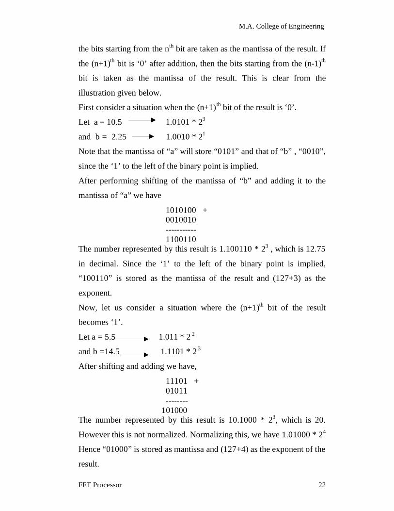
M.A. College of Engineering
FFT Processor 22
the bits starting from the nth bit are taken as the mantissa of the result. If
the (n+1)th bit is ‘0’ after addition, then the bits starting from the (n-1)th
bit is taken as the mantissa of the result. This is clear from the
illustration given below.
First consider a situation when the (n+1)th bit of the result is ‘0’.
Let a = 10.5 1.0101 * 23
and b = 2.25 1.0010 * 21
Note that the mantissa of “a” will store “0101” and that of “b” , “0010”,
since the ‘1’ to the left of the binary point is implied.
After performing shifting of the mantissa of “b” and adding it to the
mantissa of “a” we have
1010100 + 0010010 ----------- 1100110 The number represented by this result is 1.100110 * 23 , which is 12.75
in decimal. Since the ‘1’ to the left of the binary point is implied,
“100110” is stored as the mantissa of the result and (127+3) as the
exponent.
Now, let us consider a situation where the (n+1)th bit of the result
becomes ‘1’.
Let a = 5.5 1.011 * 22
and b =14.5 1.1101 * 23
After shifting and adding we have,
11101 + 01011 -------- 101000 The number represented by this result is 10.1000 * 23, which is 20.
However this is not normalized. Normalizing this, we have 1.01000 * 24
Hence “01000” is stored as mantissa and (127+4) as the exponent of the
result.

M.A. College of Engineering
FFT Processor 23
Normalizing the difference of two numbers is pretty straight forward.
Here the mantissa of the result is shifted to the left until the nth bit is ‘1’.
For each shifting the exponent is to be decremented by 1. After the nth
bit becomes ‘1’, the mantissa of the normalised result is taken from the
(n-1)th bit. This is because the ‘1’ in the nth bit is implied and does not
need to be stored.
3.3 Hardware Implementation of Floating-Point Adder
The hardware implementation of the floating-point adder unit involves
considerable circuitry. The block diagram of the implementation is
given above. Following is a description of each block of the unit. A
detailed explanation of the VHDL description of the units is also given.
Note that the adder uses two clocks. One is the main clock. Only the
control unit requires this clock. The numbers are inputted during the
positive cycle of this clock. This clock is also the clock synchronising
the various blocks of the FFT processor, which is to be discussed later
on. The other clock, which has a much shorter period, is local to the
adder. All the blocks within the adder are synchronised using this clock.
3.3.1 Block diagram of the adder
ensub ,enswap, enshift, addpulse, normalise : enables corresponding blocks.
Finsub, finswap, finshift, finish_sum, end_all : signals to indicate that the
corresponding operations in the blocks are over.
A_small : high if “a” is the smaller number.
Numzero : high when one of the numbers is zero.
Change : pulse given to control unit whenever there is a change in input numbers.
Exp : exponent of larger number.
Addsub : high if operation to be performed is addition , else it is low.
Signbit : high if sign of result is –ve. If result is positive this signal is low.
Reset : Resets the control unit.
Rst : resets all signals of all the units.

M.A. College of Engineering
FFT Processor 24
SUBTRACTOR
SUMMER
NORMALIZER
CONTROLUNIT
SHIFTER
chan
ge
num
zero
finsu
b
ensu
b
SWAP UNIT
swap
_num
1
exp
f inswap
enswap
swap
_num
2
sub
enshi f t
f inshif t
adds
ub
addp
ulse
finis
h_su
m
shift
_out
s um_ou t
normal ise signbit addsub end_al l
zero
dete
ct
f i na l_sum
a_sm
all
rst
rese
t
a (31)
b(31)
Figure 3.2 Block diagram of floating point adder unit
3.3.2 The Subtractor Unit
The function of the subtractor is to output the difference between the
mantissas of the two numbers. This information is given to the shifter,
which shifts the smaller number by the difference between the
mantissas. Apart from this, the subtractor gives information to the
control unit as to which number is smaller and if any number is zero. Let
us examine the code in detail.
The first process begins with the “if(rst_sub=’0’)” statement. This
indicates that we need to proceed only if the reset port to the unit is low.
That is if the reset port to the subtractor is high then we need only to set

M.A. College of Engineering
FFT Processor 25
the outputs to zero. Note that the ninth bit is an extra bit. This bit is set
to ‘1’ whenever there is a valid output number.
First the exponent and the mantissa are separated and written into separate
variables. Since the involvement of zero in calculations need to be treated
separately, the presence of zero in any one of the numbers is detected by the
statements “if(c=0)” and “if(d=0)”. When one of the numbers is zero, the
num_zero signal is set high. If “a” is zero then the output of “zero_detect” is
“01”. If “b” is zero then this signal is set to “10”.
Several cases arise now .If the exponents of the two numbers are different,
then the smaller one is to be found out and corresponding subtractions made. If
the exponents are same then the smaller of the mantissas is to be found out. In
certain cases the numbers are the same. All these cases need to be treated
separately. The signal “a_smaller” is used to give information to the control
unit as to which number is smaller. When the calculations are finished the
“fin_sub” signal goes high. All these signals are reset at the start of the next set
of calculations.
There is a second process , namely “process(a,b)” within the same architecture.
This process is executed whenever there is a change in the input numbers. This
process sends out a pulse called “change” to the control unit indicating that the
input numbers have changed. The control unit then restarts the entire cycle of
operations.
3.3.3 The Swap Unit
The function of the swap unit is to input the mantissa of the smaller number to
the shifter, so that it can shift it by the difference in the exponents of the two
numbers. The implicit ‘1’ in the IEEE standard format is concatenated with the
mantissa of the larger number and inputted to the summer. Also the L.S.B (last
8 bits) of the mantissa of this number is set to zero. The mantissa of the
smaller number is given to the shifter. In this case also a ‘1’ is concatenated
M.A. College of Engineering
FFT Processor 26
with the mantissa (for checking in the shifter for a valid number) and the last
nine bits are set to zero. After the swapping process is over the signal
finish_swap is set high to inform the control unit. When the rst_swap signal is
high the signals are reset.
3.3.4 The Shifter Unit
There are two “if” blocks in the shifter. This is needed because the
assignments to “sub_temp” and “temp2” in the first block get updated in
the next “if” block and multiple clock cycles may be needed to complete
the shifting process. Therefore the first “if” block needs to be executed
only the first time a number arrives . Let us examine this in detail.
Initially when the processor is reset (this is done after each addition by
the control unit) the variables “temp3” and “t” are set to ‘1’ while
“finish_out” is reset to ‘0’. Whenever there is a change in the signals
given in the sensitivity list of the process, the process is executed. The
first time , the first “if” block is executed and thereafter the second
block. However we see that “temp3” is reset to ‘0’ in the first block. So
the first block will not be executed in the next clock cycle (since this
block is executed only for “temp3=’1’) unless the block is reset (when
reset, temp3 is set to ‘1’).
In the second “if” block the unit first checks whether “sub_temp” is
zero (last 8 bits only). If so, no more shifting is required and the number
is outputted. Also finish_out is set to ‘1’. If “sub_temp” is not zero then
the mantissa is shifted to the right . At the same time “sub_temp” is
decremented. This is given by the lines
elsif ( clock = '1' and clock'event ) then
temp2 := '0' & temp2 (31 downto 1) ;
sub_temp := sub_temp - "00000001" ;

M.A. College of Engineering
FFT Processor 27
In the next clock cycle the unit will first check if “sub_temp” is zero. If
so, it outputs the shifted mantissa to the summer, else the number is
shifted again.
3.3.5 The Summer Unit
This unit sums/subtracts the shifted mantissa of the smaller number and
the mantissa of the larger number. The summer adds an extra bit ‘0’ and
then sums/subtracts. This is to find out whether normalization is
required or not. If normalization (that is converting the result to IEEE
format) is required, this bit will be set. The information as to whether
addition or subtraction is to be done is received from the control unit
from the signal “addsub”. After the addition process, the “add_finish”
signal is set.
3.3.6 The Normalize Unit
As in the case of the shifter unit, there are two “if” blocks in this section
for the same reasons as that of the shifter unit. The normalization
process when one number is zero and when addition or subtraction is
used are all different from one another. The block under
“if(addsub=’0’)” gives the normalization procedure for the difference of
two numbers. The first statement under this section is
“if(numb_temp=0)”. Such a condition occurs only when both numbers
are same and they have been subtracted (or they are of opposite sign
and they have been added). Obviously the result is zero. If a number is
normalized then numb_temp(31) is zero. In that case the final difference
can be outputted. If numb_temp(31) is not ‘1’ then it has to be shifted to
the left in successive clock cycles until this bit is ‘1’. For each shifting
the exponent is decremented by one. This is given by the section
elsif (clock = '1' and clock'event) then

M.A. College of Engineering
FFT Processor 28
numb_temp := numb_temp(30 downto 0) & '0' ;
temp_exp := temp_exp - "00000001" ;
end if ;
The normalization process of addition is different. Here, if normalisation
is required, the bit “numb_temp(32)” will be ‘1’. In that case, the
exponent has to be incremented by one. If numb_temp(32)=’0’, the bits
of the sign, exponent and the mantissa just have to concantanated.
When one of the numbers is zero, the sum is the other number. The
subtractor gives the information as to which number is zero. If “a” is
zero, “zero_detect” is “01” and the output is “b”. If “b” is zero,
“zero_detect” is “10” and the output is “a”.
3.3.7 The Control Unit
The control unit is the “H.O.D” of the floating point adder unit. It
controls all the activities of the adder. It is modelled as a finite state
machine. So first, something about finite state machines.
Finite State Machine
A finite state machine (FSM) is a type of sequential circuit that is
designed to sequence through specific patterns of finite states in a
predetermined sequential manner. There are two types of FSM, Mealy
and Moore. The Moore FSM has outputs that are a function of current
state only. The Mealy FSM has outputs that are a function of the
current state and primary inputs. An FSM consists of three parts:
1. Sequential Current State Register: The register, a set of n-bit flip-
flops
(state vector flip-flops) clocked by a single clock signal is used
to hold the state vector (current state or simply state) of the FSM. A
state vector with a length of n-bit has 2 to the power n possible binary
patterns, known as state encoding. Often, not all 2 to the power n

M.A. College of Engineering
FFT Processor 29
patterns are needed, so the unused ones should be designed not to occur
during normal operation. Alternatively, an FSM with m-state requires at
least
log2 (m) state vector flip-flops.
2. Combinational Next State Logic: An FSM can only be in one state
at any given time, and each active transition of the clock causes it
to change from its current state to the next state, as defined by the
next state logic. The next state is a function of the FSM’s inputs and
its current state.
3. Combinational Output Logic: Outputs are normally a function of
the current state and possibly the FSM’s primary inputs (in the case
of a Mealy FSM). Often in a Moore FSM, you may want to derive
the outputs from the next state instead of the current state, when
the outputs are registered for faster clock-to-out timings.
Moore and Mealy FSM structures are shown below.
M.A. College of Engineering
FFT Processor 30
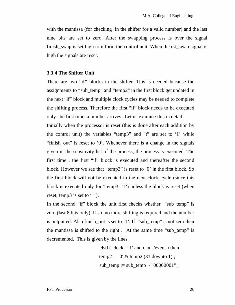
Figure 3.3 Structure of a finite state machine
The control unit is modelled as a Mealy machine. The transition from
one state to another, takes place during the rising clock edge of the
positive cycle. If there is any change in the input numbers to the
subtractor, it sends out a pulse (change) to the control unit. The control
unit then starts the FSM from the beginning. Also when the processor is
reset externally, the control unit sets the current state as the first state
(reset1). The second process carries out all these actions.
The actions performed in each state in the first process are given below:
Reset1 : Here, the various signals are reset.
Reset2 : The reset signal is brought back to ‘0’. (Otherwise the outputs
will not change, it will remain as 0). Also the subtractor and swap units
are enabled.
Reset3 : If one of the numbers is zero (indicated by “zero_num”) the
shifting and adding operations can be skipped. Therefore the next state
is set as reset5. Else, the shifter is enabled when the operations in the
subtractor and swap unit are over. Also the subtractor and swap unit are
disabled.
Reset4 : When the function of the shifter is over, it is disabled and the
adder unit is enabled.
M.A. College of Engineering
FFT Processor 31
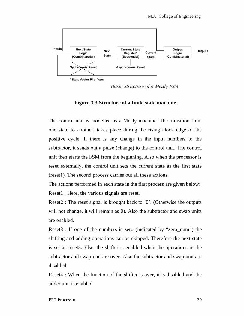
Reset5 : If one of the numbers is zero, the normalize unit is enabled.
Else, the normalize unit is enabled when the function of the summer is
over. Also, the summer is disabled in this state.
Reset6 : Here, when the normalisation process is over, the normalize
unit is disabled in the positive cycle. Later, in the negative cycle, the
state is transferred to reset1.
Reset7 : This is the state into which the control unit comes when the
adder is disabled.
There is a third process in the control unit which gives information to
the summer as to whether addition or subtraction is to be performed. It
also gives information to the normalize unit about the sign of the result.
The operation to be performed and the sign of the result are determined
from the following table.
Sign of a Sign of b Bigger number Sign of result Operation to be
performed
+ve +ve a or b +ve addition
-ve -ve a or b -ve addition
+ve -ve a -ve subtraction
-ve +ve a -ve subtraction
+ve
-ve
b
+ve
subtraction
-ve +ve b +ve subtraction

M.A. College of Engineering
FFT Processor 32
“a_small” (this signal is high if a is smaller) will be high even if both the
numbers are same. However it can be seen from the table that this does
not affect the result.
3.3.8 The Testbench for the Adder
The testbench is used to give the external inputs to the adder. It also
instantiates the various components. The input numbers are read in
through a text file. Here, each bit has to be read in and assigned to a
local variable. Then the entire string is assigned to either “a” or ”b”.
The results are obtained in a file named simili.lst (if you use VHDL
Simili for simulation). It can be examined to verify the correctness of
the design.
M.A. College of Engineering
FFT Processor 33
CHAPTER 4
THE FOURIER TRANSFORM
4.1 The Discrete Fourier Transform.
Fourier analysis is a family of mathematical techniques, all based on
decomposing signals into sinusoids. The discrete Fourier transform
(DFT) is the family member used with digitized signals. Fourier analysis
is named after Jean Baptiste Joseph Fourier (1768-1830), a French
mathematician and physicist.
4.1.1 An Illustration
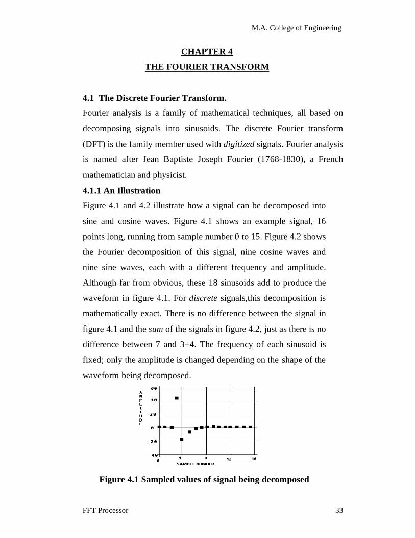
Figure 4.1 and 4.2 illustrate how a signal can be decomposed into
sine and cosine waves. Figure 4.1 shows an example signal, 16
points long, running from sample number 0 to 15. Figure 4.2 shows
the Fourier decomposition of this signal, nine cosine waves and
nine sine waves, each with a different frequency and amplitude.
Although far from obvious, these 18 sinusoids add to produce the
waveform in figure 4.1. For discrete signals,this decomposition is
mathematically exact. There is no difference between the signal in
figure 4.1 and the sum of the signals in figure 4.2, just as there is no
difference between 7 and 3+4. The frequency of each sinusoid is
fixed; only the amplitude is changed depending on the shape of the
waveform being decomposed.
Figure 4.1 Sampled values of signal being decomposed

M.A. College of Engineering
FFT Processor 34
Figure 4.2 Sine and cosine waves after Fourier decomposition
There are an infinite number of ways that a signal can be
decomposed. The goal of decomposition is to end up with something

M.A. College of Engineering
FFT Processor 35
easier to deal with than the original signal. For example, impulse
decomposition allows signals to be examined one point at a time,
leading to the powerful technique of convolution. In Fourier
Transforms, the component sine and cosine waves are simpler than the
original signal because they have a property that the original signal does
not have: sinusoidal fidelity. A sinusoidal input to a system is
guaranteed to produce a sinusoidal output. Only the amplitude and phase
of the signal can change; the frequency and wave shape must remain the
same. Sinusoids are the only waveform that have this useful property.
While square and triangular decompositions are possible, there is no
general reason for them to be useful.
4.1.2 Types of Fourier Transforms
A signal can be either continuous or discrete, and it can be either
periodic or aperiodic. The combination of these two features generates
the four categories of Fourier Transforms described below and
illustrated in Fig. 4.3
Aperiodic-Continuous
This includes, for example, decaying exponentials and the Gaussian
curve. These signals extend to both positive and negative infinity
without repeating in a periodic pattern. The Fourier Transform for this
type of signal is simply called the Fourier Transform.
Periodic-Continuous
Here the examples include: sine waves, square waves, and any
waveform that repeats itself in a regular pattern from negative to
positive infinity. This version of the Fourier transform is called the
Fourier Series.
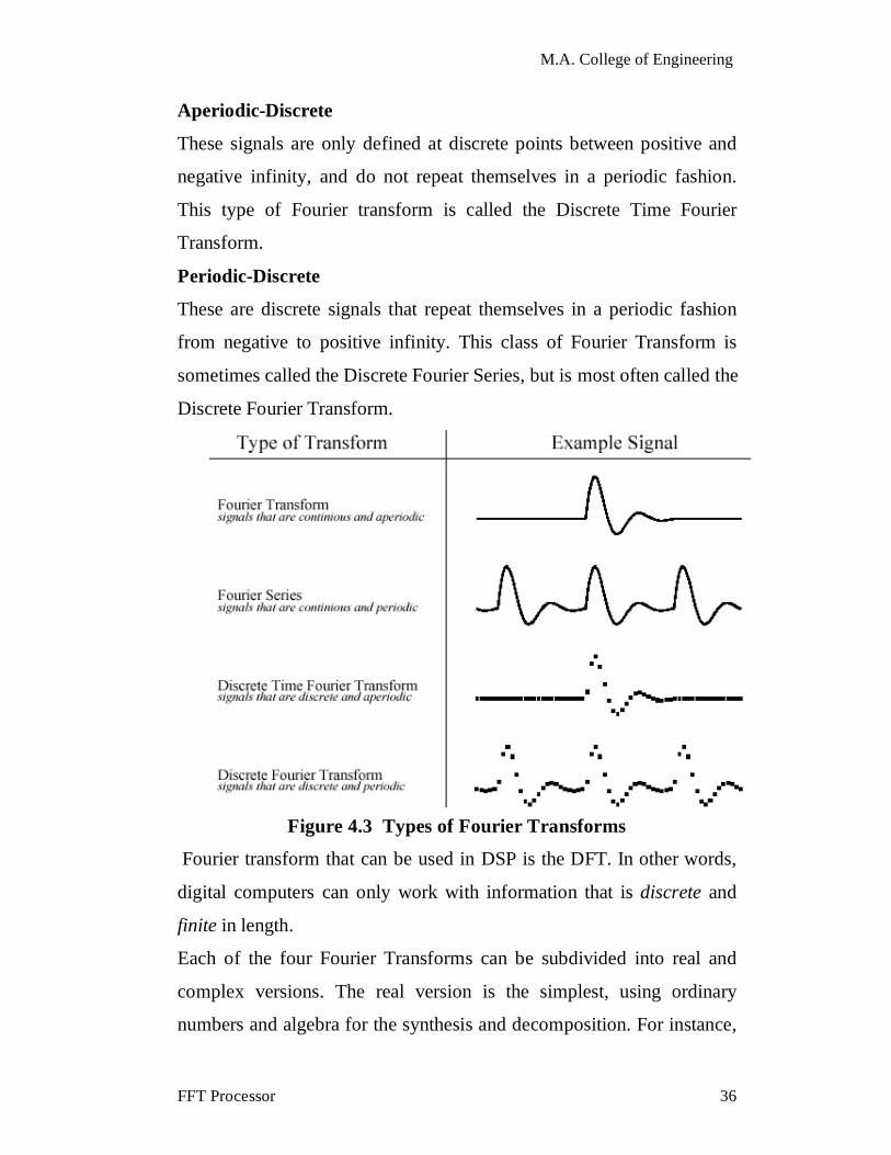
M.A. College of Engineering
FFT Processor 36
Aperiodic-Discrete
These signals are only defined at discrete points between positive and
negative infinity, and do not repeat themselves in a periodic fashion.
This type of Fourier transform is called the Discrete Time Fourier
Transform.
Periodic-Discrete
These are discrete signals that repeat themselves in a periodic fashion
from negative to positive infinity. This class of Fourier Transform is
sometimes called the Discrete Fourier Series, but is most often called the
Discrete Fourier Transform.
Figure 4.3 Types of Fourier Transforms
Fourier transform that can be used in DSP is the DFT. In other words,
digital computers can only work with information that is discrete and
finite in length.
Each of the four Fourier Transforms can be subdivided into real and
complex versions. The real version is the simplest, using ordinary
numbers and algebra for the synthesis and decomposition. For instance,
M.A. College of Engineering
FFT Processor 37
Fig. 4.1 is an example of the real DFT. The complex versions of the four
Fourier transforms are immensely more complicated, requiring the use
of complex numbers. These are numbers such as:3+4j , where j is equal
to root of-1 (electrical engineers use the variable j, while
mathematicians use the variable, i). Complex mathematics can quickly
become overwhelming, even to those that specialize in DSP.
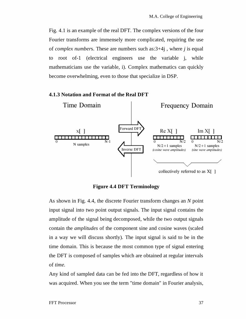
4.1.3 Notation and Format of the Real DFT
Figure 4.4 DFT Terminology
As shown in Fig. 4.4, the discrete Fourier transform changes an N point
input signal into two point output signals. The input signal contains the
amplitude of the signal being decomposed, while the two output signals
contain the amplitudes of the component sine and cosine waves (scaled
in a way we will discuss shortly). The input signal is said to be in the
time domain. This is because the most common type of signal entering
the DFT is composed of samples which are obtained at regular intervals
of time.
Any kind of sampled data can be fed into the DFT, regardless of how it
was acquired. When you see the term "time domain" in Fourier analysis,

M.A. College of Engineering
FFT Processor 38
it may actually refer to samples taken over time, or it might be a general
reference to any discrete signal that is being decomposed. The term
frequency domain is used to describe the amplitudes of the sine and
cosine waves . The number of samples in the time domain is usually
represented by the variable N. In most cases, the samples run from 0 to
N-1, rather than 1 to N.
Standard DSP notation uses lower case letters to represent time domain
signals, such as x[ ],y[ ] , and z[ ] . The corresponding upper case letters
are X[ ] Y[ ] Z[ ], used to represent their frequency domains, that is X[ ],
Y[ ], Z[ ].For illustration, assume an N point time domain signal is
contained in x[ ]. The frequency domain of this signal is called X[ ], and
consists of two parts, each an array of N/2+1 samples . These are called
the Real part of X[ ] ,written
as Re X[ ] , and the Imaginary part of X[ ], written as Im X[ ] . The
values Re X[ ] are the amplitudes of the cosine waves, while the values
in Im X[ ]are the amplitudes of the sine waves.
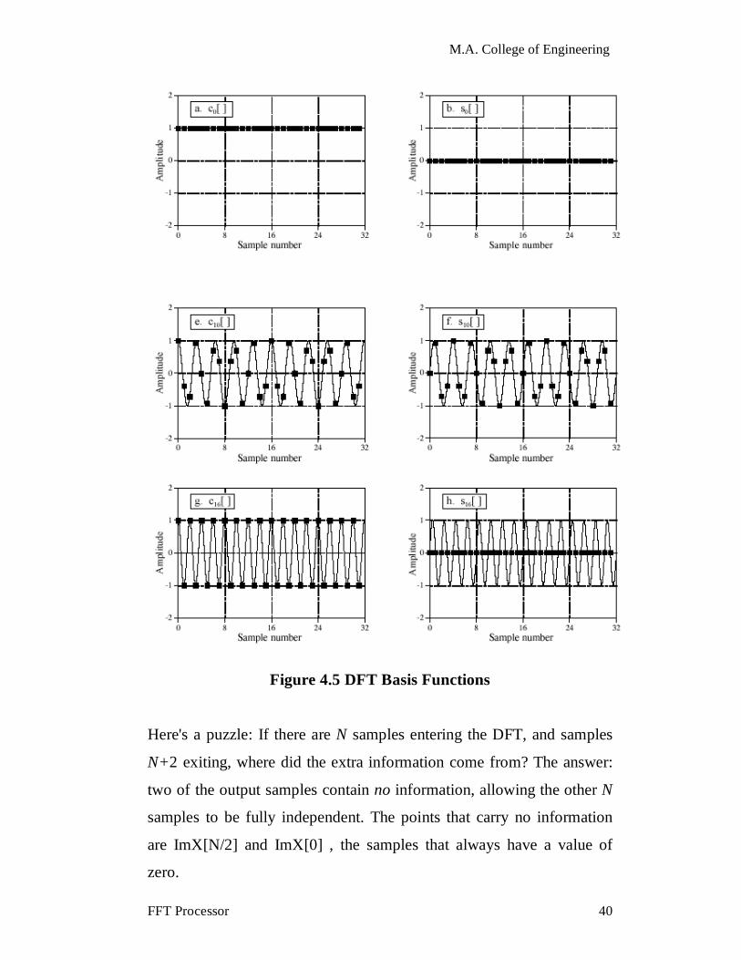
4.1.4 DFT Basis Functions
The sine and cosine waves used in the DFT are commonly called the
DFT basis functions. In other words, the output of the DFT is a set of
numbers that represent amplitudes. The basis functions are a set of sine
and cosine waves with unity amplitude. If you assign each amplitude
(the frequency domain) to the proper sine or cosine wave (the basis
functions), the result is a set of scaled sine and cosine waves that can be
added to form the time domain signal.
The DFT basis functions are generated from the equations:
Ck[ i ] = cos(2 pi k i /N)
Sk[ i ] = sin (2 pi k i /N)
M.A. College of Engineering
FFT Processor 39
where Ck[ ] is the cosine wave for the amplitude held in Re X[k], and
Sk[ ] is the sine wave for the amplitude held in Im X[k]. Each is N points
in length, running from i = 0 to N-1. The parameter, k, determines the
frequency of the wave. In an N point DFT ,k takes on values between 0
and N/2. The DFT basis functions are illustrated in figure 4.5.
Let's look at several of these basis functions in detail. Figure (a) shows
the cosine wave c0[]. This is a cosine wave of zero frequency, which is a
constant. This means that it holds the average value of all the points in
the time domain signal. In electronics, it would be said that ReX[0]
holds the DC offset. The sine wave of zero frequency, s0[] is shown in
(b), and is composed of all zeros. Since this can not affect the time
domain signal being synthesized, its value is irrelevant, and always set
to zero.
Figures (c) & (d) show c10[]&s10[] the sinusoids that complete ten cycles
in the N points. These correspond to ReX[10] & ImX[10] , respectively.
The highest frequencies in the basis functions are shown in (g) and (h).
These are cN/2[] & sN/2[] or in this example, c16[]& s16[]. This discrete
cosine wave alternates in value between 1 and -1, which can be
interpreted as sampling a continuous sinusoid at the peaks. In contrast,
the discrete sine wave contains all zeros, resulting from sampling at the
zero crossings. This makes the value of ImX[N/2] the same as ImX[0],
always equal to zero, and does not affect the synthesis of the time
domain signal.
M.A. College of Engineering
FFT Processor 40
Figure 4.5 DFT Basis Functions
Here's a puzzle: If there are N samples entering the DFT, and samples
N+2 exiting, where did the extra information come from? The answer:
two of the output samples contain no information, allowing the other N
samples to be fully independent. The points that carry no information
are ImX[N/2] and ImX[0] , the samples that always have a value of
zero.

M.A. College of Engineering
FFT Processor 41
4.1.5 Analysis, Calculating the DFT
The DFT analysis equations are given below. Here, x[i] is the time
domain signal being analyzed. ReX[k] and ImX[k] are the frequency
domain signals being calculated. The index i runs from 0 to N-1 while k
runs from 0 to N/2.
The DFT can be calculated in three completely different ways. First, the
problem can be approached as a set of simultaneous equations.
Thismethod is useful for understanding the DFT, but it is too inefficient
to beof practical use. The second method is called correlation. This is
based on detecting a known waveform in another signal. The third
method, called the Fast Fourier Transform (FFT), is an ingenious
algorithm that decomposes a DFT with N points, into N DFTs each with
a single point. The FFT is typically hundreds of times faster thanthe
other methods. It is important to remember that all three of these
methods produce an identical output. In actual practice, correlation is
the preferred technique if the DFT has less than about 32 points,
otherwise the FFT is used.
4.2 THE FAST FOURIER TRANSFORM
J.W. Cooley and J.W. Tukey are given credit for bringing the FFT to the
world in their paper: "An algorithm for the machine calculation of
complex Fourier Series," Mathematics Computation. The FFT is based
on the complex DFT, a more sophisticated version of the real DFT.
M.A. College of Engineering
FFT Processor 42
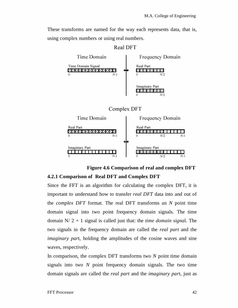
These transforms are named for the way each represents data, that is,
using complex numbers or using real numbers.
Figure 4.6 Comparison of real and complex DFT
4.2.1 Comparison of Real DFT and Complex DFT
Since the FFT is an algorithm for calculating the complex DFT, it is
important to understand how to transfer real DFT data into and out of
the complex DFT format. The real DFT transforms an N point time
domain signal into two point frequency domain signals. The time
domain N/ 2 + 1 signal is called just that: the time domain signal. The
two signals in the frequency domain are called the real part and the
imaginary part, holding the amplitudes of the cosine waves and sine
waves, respectively.
In comparison, the complex DFT transforms two N point time domain
signals into two N point frequency domain signals. The two time
domain signals are called the real part and the imaginary part, just as

M.A. College of Engineering
FFT Processor 43
are the frequency domain signals. In spite of their names, all of the
values in these arrays are just ordinary numbers. Suppose there is an N
point signal, and we need to calculate the real DFT by using the FFT,
then set all of the samples in the imaginary part to zero. Then, move the
N point signal into the real part of the complex DFT's time domain, and
compute DFT using the FFT. The result is a real and an imaginary signal
in the frequency domain, each composed of N points. Samples 0 through
N/2 of these signals correspond to the real DFT's spectrum .
4.2.2 How the FFT works
The FFT is a complicated algorithm, and its details are usually left to
those that specialize in such things. This section describes the general
operation of the FFT. The FFT operates by decomposing an N point
time domain signal into N time domain signals each composed of a
single point. The second step is to calculate the N frequency spectra
corresponding to these N time domain signals. Lastly, the N spectra are
synthesized into a single frequency spectrum. There are basically two
algorithms in FFT. One is called DIT(Decimation in time) and the other
DIF(Decimation in frequency).
In the DIT approach, the initial DFT is divided into two transforms, one
consisting of a transform of even samples and the other consisting of a
transform of odd samples. This process is carried out until the initial
transform is reduced to a set of two-point transforms of the initial data.
An in-place FFT implementation allows the results of each FFT
butterfly to replace its inputs. In order to use an in place algorithm it is
necessary either to re-order the input data array or re-order the output
array. This re-ordering is simply arranged by reversing the address bits.
Before starting to calculate the DFT, the input data is ordered such that
its address is bit-reversed, that is if the binary address of the required

M.A. College of Engineering
FFT Processor 44
sequence of data is 110 then the bit reversed version on that becomes
011. Given below is the signal flow graph for the DIT.
Figure 4.7 Signal flow graph for 8 point DIT-FFT with input
scrambling
This signal flow graph consists of a number of butterflies. Each butterfly
takes a pair of input data values A and B and outputs A1 and B1 as
shown below. The input data is multiplied by the twiddle factor WNk .
The solid dots represent addition\subtraction.
where
A= x + jX
B= y + jY
WNk � �������� – ��������
A1 = x1 + jX 1 = A + BWNk
B1= y1 + jY 1 = A - BWNk
Subsituting for A , B and WNk we obtain

M.A. College of Engineering
FFT Processor 45
A1����������� ��������� �������������� ��-������ ����
B1=[(x-������ ��-������ ������X-������ �� � ������ ����
An in-place algorithm makes efficient use of memory as the transformed
data overwrites the input data. However the indexing required to
determine which location in memory to fetch the input data is quite
complex. This is explained later on when the processor is discussed.
The algorithm used in this processor is a variation of the DIT algorithm
discussed above. The difference is that output scrambling is used and the
inputs are in natural order. The signal flow graph for this algorithm is
shown below.
Figure 4.8 Signal flow graph for modified DIT-FFT
with output scrambling
An illustration of the modified version of the FFT-DIT algorithm is
given below. The inputs are first stored in the addresses shown. The
results of FFT computation at each stage is shown. The results of the
final stage are outputted in a bit reversed addresses.

M.A. College of Engineering
FFT Processor 46
4.3 Synthesis, Calculating the Inverse DFT
The synthesis equation is given as
In words, any N point signal, can be created by adding N/2 + 1 cosine
waves and N/2+1 sine waves. The amplitudes of the cosine and sine
waves are held in the arrays ReX[k](bar) and ImX[k](bar), respectively.
The synthesis equation multiplies these amplitudes by the basis
Addr
ess Input
O/P of
Stage 1
O/P of
stage 2
O/P of
stage 3
Bit-reversed
O/P
0000 -1 -3 -2.5 0 0
0001 1 -0.5 2.5 -5 2.06065
0010 1.5 0.5 -3.5 -3.5 -3.5
0011 2 3 -3.5 -3.5 -0.06065
0100 -2 1 1 2.06065 -5
0101 -1.5 2.5 2.5 -0.06065 -0.06065
0110 -1 2.5 1 -0.06065 -3.5
0111 1 1 2.5 2.06065 2.06065
1000 0 0 0 0 0
1001 0 0 0 0 -4.9749
1010 0 0 0 3.5 3.5
1011 0 0 0 -3.5 0.02515
1100 0 0 -2.5 -4.9749 0
1101 0 0 -1 -0.02515 -0.2515
1110 0 0 2.5 0.02515 -3.5
1111 0 0 1 4.9749 4.9749

M.A. College of Engineering
FFT Processor 47
functions to create a set of scaled sine and cosine waves. Adding the
scaled sine and cosine waves produces the time domain signal, x[ i].
In the equation given above, the arrays are called ReX[k](bar) and
ImX[k](bar), rather than ReX[k] and ImX[k], This is because the
amplitudes needed for synthesis are slightly different from the
frequency domain ReX[k] and ImX[k], of a signal . This is the scaling
Im X[ k] Re X[ k] factor issue we referred to earlier. Although the
conversion is only a simple normalization, it is a common bug in
computer programs. The conversion between the two is given by
ReX[k](bar) = ReX[k]/(N/2)
ImX[k](bar) = -ImX[k]/(N/2)
except for two special cases
ReX[0](bar) = ReX[0]/N
ReX[N/2](bar) = ReX[N/2]/N
The conversion is required because the frequency domain is defined as
a spectral density. Figure 4.9 shows how this works. Spectral density
describes how much signal (amplitude) is present per unit of bandwidth.
To convert the sinusoidal amplitudes into a spectral density, divide each
amplitude by the bandwidth represented by each amplitude. This brings
up the next issue: how do we determine the bandwidth of each of the
discrete frequencies in the frequency domain? As shown in the figure,
the bandwidth can be defined by drawing dividing lines between the
samples. For instance, sample number 5 occurs in the band between 4.5
and 5.5; sample number 6 occurs in the band between 5.5 and 6.5, etc.
Expressed as a fraction of the total bandwidth (i.e., N/2), bandwidth of
each sample is 2/N. An exception to this is the samples on each end,
which have one-half of this bandwidth, 1/N. This accounts for the
scaling factor between the sinusoidal amplitudes and frequency domain,
as well as the additional factor of two needed for the first and last

M.A. College of Engineering
FFT Processor 48
samples. Why the negation of the imaginary part? This is done solely to
make the real DFT consistent with its big brother, the complex DFT.
Figure 4.9 The bandwidth of frequency domain signals
4.4 Illustration of the DFT and IDFT in Matlab
Given below is an illustration of the DFT and IDFT in Matlab using an
8-point sample. The commands and the results are given.
» p=[-1.2 2 3 -2 0 4 -0.23 1]; %sampled input
» y=fft(p); %command to find the fft
» disp(y); % display y
Columns 1 through 4
6.5700 -0.4929 + 0.3055i -3.9700 - 7.0000i -1.9071 + 6.7655i
Columns 5 through 8
-3.4300 -1.9071 - 6.7655i -3.9700 + 7.0000i -0.4929 - 0.3055i
% The commands below calculate the time domain signal from the
% frequency domain signals obtained above.
% The following lines take into account the scaling factors.
» cosines=real(y)/4; % divide real parts of fft result by N/2
» sines=-imag(y)/4; % divide imaginary parts of fft result –N/2
» %special cases of scaling factors are given below
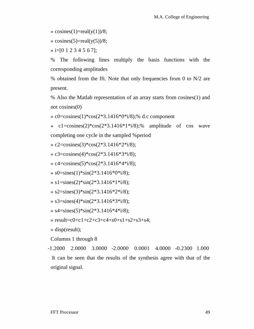
M.A. College of Engineering
FFT Processor 49
» cosines(1)=real(y(1))/8;
» cosines(5)=real(y(5))/8;
» i=[0 1 2 3 4 5 6 7];
% The following lines multiply the basis functions with the
corresponding amplitudes
% obtained from the fft. Note that only frequencies from 0 to N/2 are
present.
% Also the Matlab representation of an array starts from cosines(1) and
not cosines(0)
» c0=cosines(1)*cos(2*3.1416*0*i/8);% d.c component
» c1=cosines(2)*cos(2*3.1416*1*i/8);% amplitude of cos wave
completing one cycle in the sampled %period
» c2=cosines(3)*cos(2*3.1416*2*i/8);
» c3=cosines(4)*cos(2*3.1416*3*i/8);
» c4=cosines(5)*cos(2*3.1416*4*i/8);
» s0=sines(1)*sin(2*3.1416*0*i/8);
» s1=sines(2)*sin(2*3.1416*1*i/8);
» s2=sines(3)*sin(2*3.1416*2*i/8);
» s3=sines(4)*sin(2*3.1416*3*i/8);
» s4=sines(5)*sin(2*3.1416*4*i/8);
» result=c0+c1+c2+c3+c4+s0+s1+s2+s3+s4;
» disp(result);
Columns 1 through 8
-1.2000 2.0000 3.0000 -2.0000 0.0001 4.0000 -0.2300 1.000
It can be seen that the results of the synthesis agree with that of the
original signal.
M.A. College of Engineering
FFT Processor 50
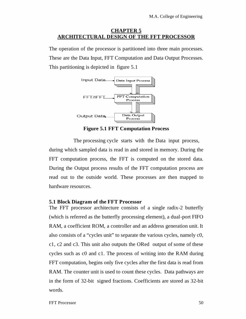
CHAPTER 5 ARCHITECTURAL DESIGN OF THE FFT PROCESSOR
The operation of the processor is partitioned into three main processes.
These are the Data Input, FFT Computation and Data Output Processes.
This partitioning is depicted in figure 5.1
Figure 5.1 FFT Computation Process
The processing cycle starts with the Data input process,
during which sampled data is read in and stored in memory. During the
FFT computation process, the FFT is computed on the stored data.
During the Output process results of the FFT computation process are
read out to the outside world. These processes are then mapped to
hardware resources.
5.1 Block Diagram of the FFT Processor The FFT processor architecture consists of a single radix-2 butterfly
(which is referred as the butterfly processing element), a dual-port FIFO
RAM, a coefficient ROM, a controller and an address generation unit. It
also consists of a “cycles unit” to separate the various cycles, namely c0,
c1, c2 and c3. This unit also outputs the ORed output of some of these
cycles such as c0 and c1. The process of writing into the RAM during
FFT computation, begins only five cycles after the first data is read from
RAM. The counter unit is used to count these cycles. Data pathways are
in the form of 32-bit signed fractions. Coefficients are stored as 32-bit
words.

M.A. College of Engineering
FFT Processor 51
CONTROLLER
BUTTERFLYPROCESSING
ELEMENT
ADDRESSGENERATION
UNIT
CO-EFFICIENT ROM
RAM
CYCLES UNIT
CO
UN
TER
stag
ed
fftd iod ipop
fft_e
n
io_m
ode
rom
gen_
en
enbw
enbor
ram
_wr
ram
_rd
rom
_en
pres
et
c0_e
n
cycles
c0\c lock
rom_add
clk_count
disable
reset_count
data
_rom
out_
data
ram
_dat
a
data_io
Figure 5.2 Block diagram of FFT Processor
A brief description of the important signals used in the processor is given below.
staged : goes high when a stage is completed
fftd : goes high when the fft operation is completed
iod : goes high when input/output operation is over.
fft_en : enable the address generation for collecting data from RAM during FFT
calculation.
io_mode : High when input/output operation is going on.
op : High when output is going on.

M.A. College of Engineering
FFT Processor 52
ip : high when input is going on.
romgen_en : enable address generation for ROM.
ram_rd : RAM read address.
ram_wr : RAM write address.
enbw : write enable of RAM
enbor : read enable of RAM
out_data : Data to be written to RAM
data_ram : Data from RAM to butterfly processing unit.
cycles : consists of signals c0,c1,c2,c3,c0_c1,c2_c3,c0_c2,c1_c3.
Note that the clock and initialising signals are not sho wn.
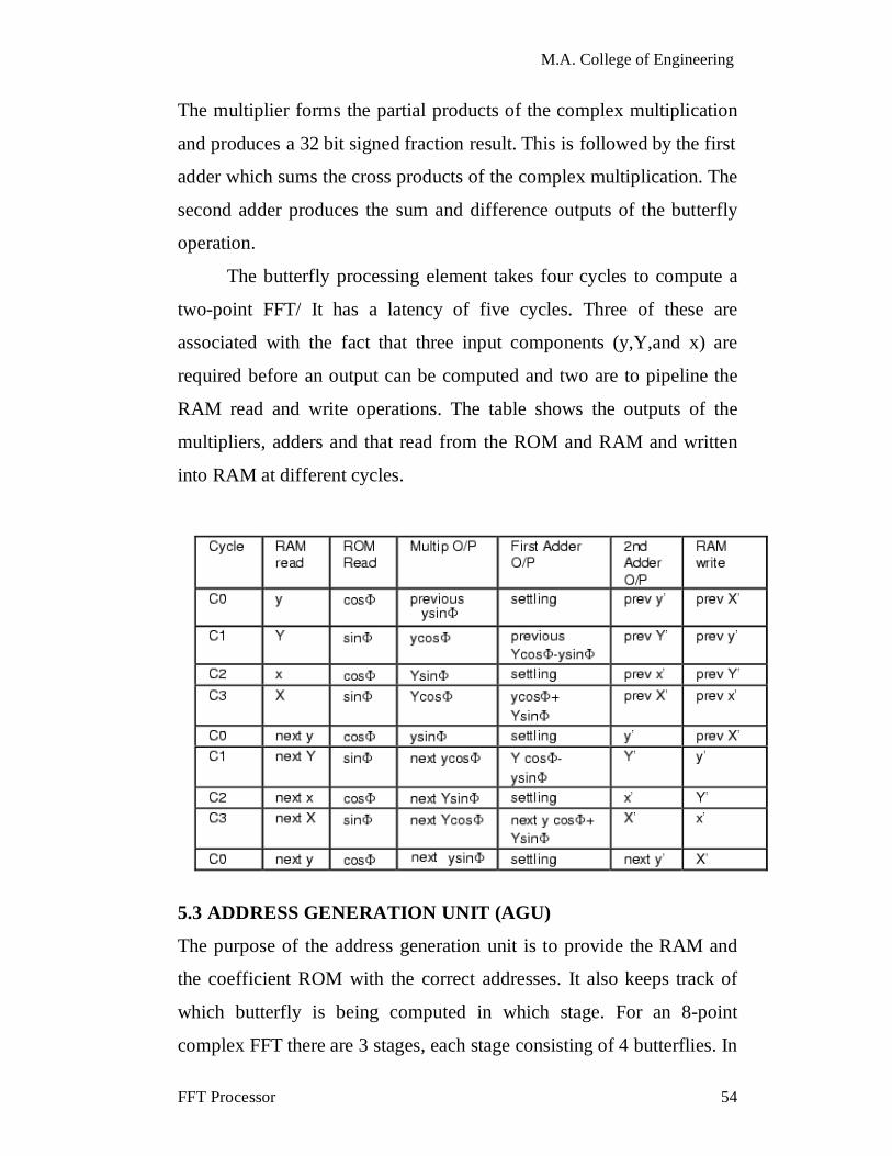
5.2 BUTTERFLY PROCESSING ELEMENT .
Figure 5.3 Butterfly Processing Unit
The butterfly is the basic operator of the FFT. It computes a two
point FFT. It takes two data words from memory and computes the FFT.
The results are written back to the same memory locations of the inputs
since an in-place algorithm is used. The butterfly processing element
computes one butterfly every four cycles. It consists of one multiplier
and two adders. The architecture for it is depicted in figure 5.3

M.A. College of Engineering
FFT Processor 53
The blocks named “R” are a set of negative edge triggered D flip
flops. That is, each “R” block consists of 32 D-flip flops, one for each
bit. Similarly the “L” blocks are positive level triggered. The blocks
labeled “D” are positive edge triggered. c0,c1,c2 and c3 are the four
cycles that the processor takes to calculate the fft . c0,c1 is the OR
output of the cycles c0 and c1. Similarly c0,c2 is the OR output of c0
and c2 and so forth. This is shown below.
c lock_main
c0
c1
c2
c3
c0,c1
Figure 5.4 Waveform of the cycles used in the FFT Processor
M.A. College of Engineering
FFT Processor 54
The multiplier forms the partial products of the complex multiplication
and produces a 32 bit signed fraction result. This is followed by the first
adder which sums the cross products of the complex multiplication. The
second adder produces the sum and difference outputs of the butterfly
operation.
The butterfly processing element takes four cycles to compute a
two-point FFT/ It has a latency of five cycles. Three of these are
associated with the fact that three input components (y,Y,and x) are
required before an output can be computed and two are to pipeline the
RAM read and write operations. The table shows the outputs of the
multipliers, adders and that read from the ROM and RAM and written
into RAM at different cycles.
5.3 ADDRESS GENERATION UNIT (AGU)
The purpose of the address generation unit is to provide the RAM and
the coefficient ROM with the correct addresses. It also keeps track of
which butterfly is being computed in which stage. For an 8-point
complex FFT there are 3 stages, each stage consisting of 4 butterflies. In

M.A. College of Engineering
FFT Processor 55
addition to this, since address generation during input, output and FFT
computation processes are different, it keeps track of the mode of
operation of the chip and generates the required address. Mode of
operation information is supplied by the controller. A block level
description of the AGU is shown in figure. The different blocks of the
AGU are explained separately.
STAGEGENER-
ATOR
incr
c lear
staged
butterf ly_iod
BUTTERFLY
GENERATOR
STAGE DONE_IO DONE
BASEINDEXGENERATOR
IO ADDRESSGENERATOR
ROM ADDRESSGENERATOR
SHIFTERS
mux
stage
incr
io_mode
stagediodfftd
butterfly
stage
staged
clear
butterfly
stage
fft_en
cycles(c0,c1,c2,c3)
io_mode
ip
op
butterfly
f f tadd_rd
io_add
io_modestage
butterfly
cycles(c0,c1,c2,c3)
romadd_genrom_add
ram_rd
ram_wr
Figure 5.5 Address Generation Unit
M.A. College of Engineering
FFT Processor 56
5.3.1 Butterfly Generator
The butterfly generator keeps track of which butterfly is being computed
in a particular stage. It is basically a 16-bit up counter since for an 8-
point complex FFT there are 4 butterflies per stage and 4 data words per
butterfly (2 real and 2 imaginary).
Note that during data input and data output the butterfly is incremented
by the clock while during fft computation mode, it is incremented by c0.
This is because, 4 cycles are required to calculate one butterfly. Hence
the butterfly generator need to be incremented only once in every 4
cycles during FFT computation. The selection between the clock and
“c0” is made by a multiplexer. The “io mode” signal is used for
selection. Whenever “clear” or “stage done” signal goes high, the
butterfly generator is reset. The block diagram of the butterfly generator
is shown above.
5.3.2 Stage Generator
The stage generator keeps track of the current stage in the FFT
computation. The stage generator supplies the base index generator with
the number of the stage which is currently being computed. For an 8-
point FFT there are 3 stages hence the stage generator is basically a two-
bit counter which is incremented one every 4 butterfly counts (by the
“stage done” signal).
5.3.3 Stage done_IO done block
It generates four signals called “iod”, “staged” “fftd” and “butterfly”.
“iod” is generated when the “butterfly” count is 15. This informs the
controller that either the Data Input or Output process is finished. The
“staged” signal is generated when the current “butterfly” count is 4, it
increments the stage generator by one. fftd is generated when the stage
M.A. College of Engineering
FFT Processor 57
count is three. This informs the controller that the FFT computation
process is done, hence forcing the FFT processor to start the data output
process. The block diagram of stage generator is shown below.
5.3.4 IO-Address Generator
The IO Address Generator is responsible for generating addresses
for RAM during the data input and output processes. During the data
input process the output of the butterfly generator “butterfly” can be
used for addressing 16 locations in the RAM. However, during the data
output process data should be bit-reversed while being written to outside
world. Once in the output process bit-reversed address is selected by the
muxes in the AGU. The controller gives the information whether the
process is in IO-mode through the signal “iomode”. This signal is used
for selecting.
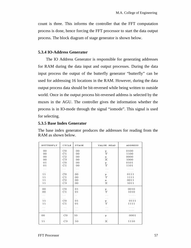
5.3.5 Base Index Generator
The base index generator produces the addresses for reading from the RAM as shown below.

M.A. College of Engineering
FFT Processor 58
The butterfly has two complex data inputs A and B. These inputs
when manipulated produces four outputs x, X, y and Y, out of which X
and Y are complex values. Since there are 16 locations, the BIG is a
mode-16 counter. The FFT mode address generation is quite complex.
The address generation is obtained by manipulating the outputs of the
butterfly generator, stage generator and the cycles.
Let the 4 bits of the butterfly signal be “b3 b2 b1 b0”. Then the addresses for “x”, “X” , “y” and “Y” are generated based on the following table. Stage Address for “x” Stage Address for “y”
1 0 0 b1 b0 1 0 1 b1 b0 2 0 b1 0 b0 2 0 b1 1 b0 3 0 b1 b0 0 3 0 b1 b0 1
The addresses for “X” and “Y” are obtained by setting the M.S.B as ‘1’
in the addresses of “x” and “y” respectively. Note that “y” is collected
from RAM during cycle “c0”. Similarly “x” is collected during the cycle
“c2” and so forth. This information is used while writing the VHDL
code.
5.3.6 The Shifters
As mentioned, the result of FFT computation is written back into the
same location as it was read. However there is a latency of five cycles.
For example, if “y” is read from the RAM during cycle “c0”, “y1” is
written into the same location as it was read after 5 cycles, that is during
cycle “c1”. So the read address is shifted in each on these five cycles.
The output of the last shifter is then given as the write address.
5.3.7 ROM Address Generator
The ROM Address Generator is used to provide the ROM with the
correct address for collecting the sine and cosine co-efficients. It is
modeled based on the co-efficients given in the signal flow graph.

M.A. College of Engineering
FFT Processor 59
5.4 CONTROLLER
The controller is modeled as a finite state machine which has been
explained already. It has seven states ranging from rst1 to rst 7. The
actions performed in each state is clearly commented in the code. The
signals to and from the controller are given in figure 5.2.
5.5 RAM AND ROM
The input is first written into the RAM. During the FFT computation
process, the FFT of two numbers is calculated and written back into the
same location in the RAM. During the output process bit reversed
address is given to the RAM and it outputs the data in it accordingly.
The ROM is used to store the sine and cosine values needed in the
FFT computation process. It outputs these values according to the
address given to it.
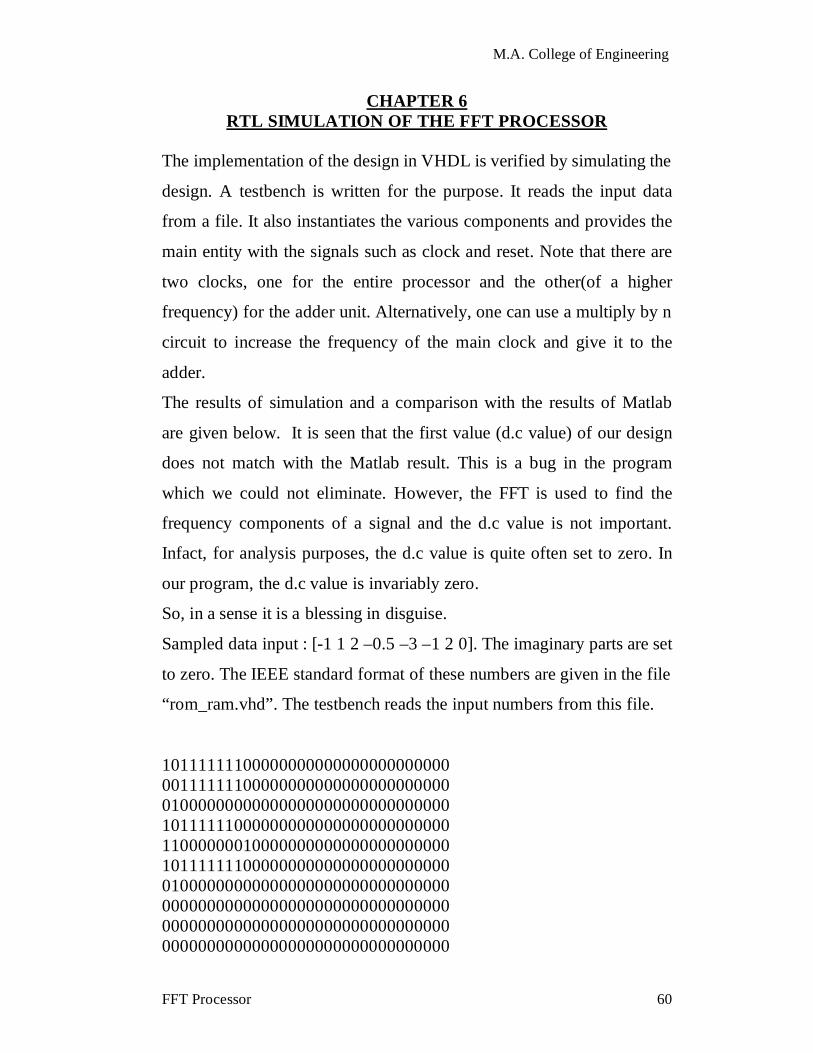
M.A. College of Engineering
FFT Processor 60
CHAPTER 6 RTL SIMULATION OF THE FFT PROCESSOR
The implementation of the design in VHDL is verified by simulating the
design. A testbench is written for the purpose. It reads the input data
from a file. It also instantiates the various components and provides the
main entity with the signals such as clock and reset. Note that there are
two clocks, one for the entire processor and the other(of a higher
frequency) for the adder unit. Alternatively, one can use a multiply by n
circuit to increase the frequency of the main clock and give it to the
adder.
The results of simulation and a comparison with the results of Matlab
are given below. It is seen that the first value (d.c value) of our design
does not match with the Matlab result. This is a bug in the program
which we could not eliminate. However, the FFT is used to find the
frequency components of a signal and the d.c value is not important.
Infact, for analysis purposes, the d.c value is quite often set to zero. In
our program, the d.c value is invariably zero.
So, in a sense it is a blessing in disguise.
Sampled data input : [-1 1 2 –0.5 –3 –1 2 0]. The imaginary parts are set
to zero. The IEEE standard format of these numbers are given in the file
“rom_ram.vhd”. The testbench reads the input numbers from this file.
10111111100000000000000000000000 00111111100000000000000000000000 01000000000000000000000000000000 10111111000000000000000000000000 11000000010000000000000000000000 10111111100000000000000000000000 01000000000000000000000000000000 00000000000000000000000000000000 00000000000000000000000000000000 00000000000000000000000000000000
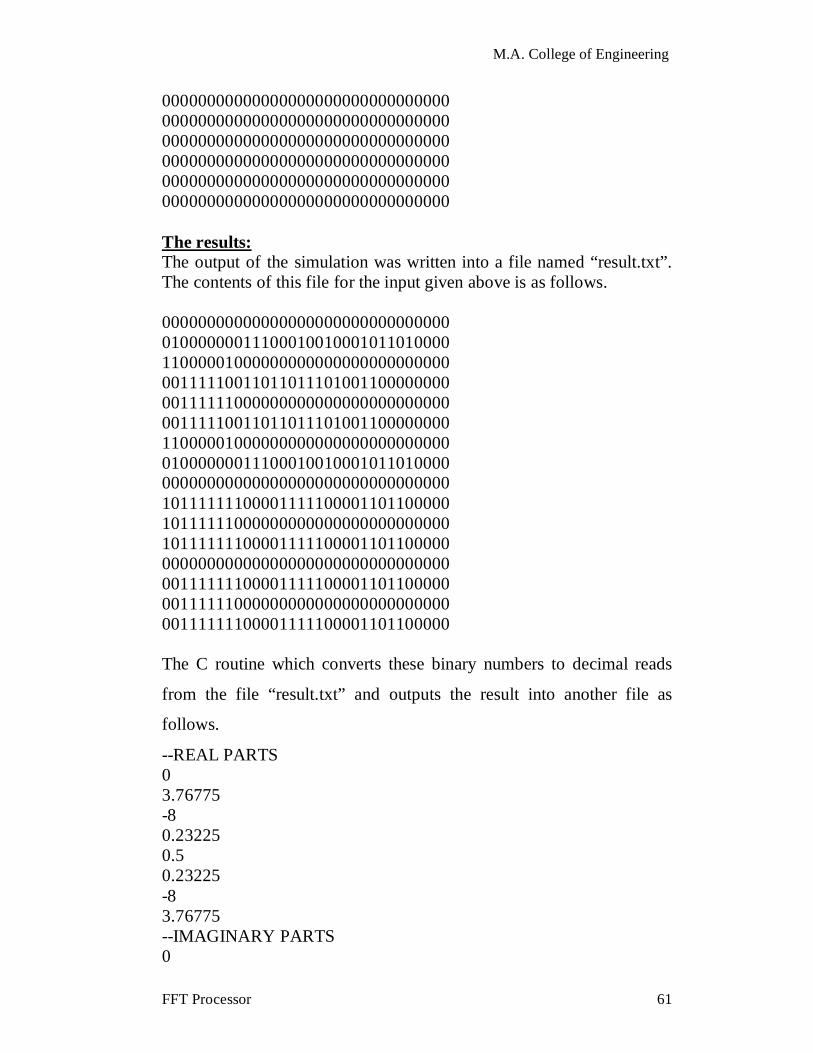
M.A. College of Engineering
FFT Processor 61
00000000000000000000000000000000 00000000000000000000000000000000 00000000000000000000000000000000 00000000000000000000000000000000 00000000000000000000000000000000 00000000000000000000000000000000 The results: The output of the simulation was written into a file named “result.txt”. The contents of this file for the input given above is as follows. 00000000000000000000000000000000 01000000011100010010001011010000 11000001000000000000000000000000 00111110011011011101001100000000 00111111000000000000000000000000 00111110011011011101001100000000 11000001000000000000000000000000 01000000011100010010001011010000 00000000000000000000000000000000 10111111100001111100001101100000 10111111000000000000000000000000 10111111100001111100001101100000 00000000000000000000000000000000 00111111100001111100001101100000 00111111000000000000000000000000 00111111100001111100001101100000 The C routine which converts these binary numbers to decimal reads
from the file “result.txt” and outputs the result into another file as
follows.
--REAL PARTS 0 3.76775 -8 0.23225 0.5 0.23225 -8 3.76775 --IMAGINARY PARTS 0

M.A. College of Engineering
FFT Processor 62
-1.06065 -0.5 -1.06065 0 1.06065 0.5 1.06065 Matlab Results
Columns 1 through 4 -0.5000 3.7678 - 1.0607i -8.0000 - 0.5000i 0.2322 - 1.0607i Columns 5 through 8 0.5000 0.2322 + 1.0607i -8.0000 + 0.5000i 3.7678 + 1.0607i

M.A. College of Engineering
FFT Processor 63
CHAPTER 7
SYNTHESIS OF THE FFT PROCESSOR The processor was synthesised using Synopsis’ FPGA Express for the
FLEX 10K family of Altera’s FPGAs. The adder unit, the butterfly
processor unit and the address generation unit were synthesised
separately. Then, the entire design was synthesised. The synthesis
software produces a number of files of which the synthesis report file
and the EDIF netlist file are important. The report file is given in
appendix B. The EDIF netlist file is too large to be given (It has more
than 1 lakh lines!). It also produces some schematics as its output. We
tried to place and route the processor using Altera’s MAX PLUS- II
tool. However, the design did not fit into any of the available devices.
The tool used was a shareware version and so only smaller designs
could be place and routed.
M.A. College of Engineering
FFT Processor 64
CONCLUSION
An 8 point 32 bit FFT processor was designed, simulated and
synthesized using VHDL. First, a VHDL by example approach was used
to illustrate the basics of VHDL. For this a floating point adder unit was
designed and tested. The FFT processor was then simulated. The results
of the simulation were seen to match with the results of Matlab. It was
synthesized and optimized for speed using Synopsis’ FPGA Express.
The chip is expected to run at a clock frequency of about 25 MHz. The
chip can be easily upgraded for a 128 point or 256 point FFT.

M.A. College of Engineering
FFT Processor 65