Embed Size (px)
Citation preview
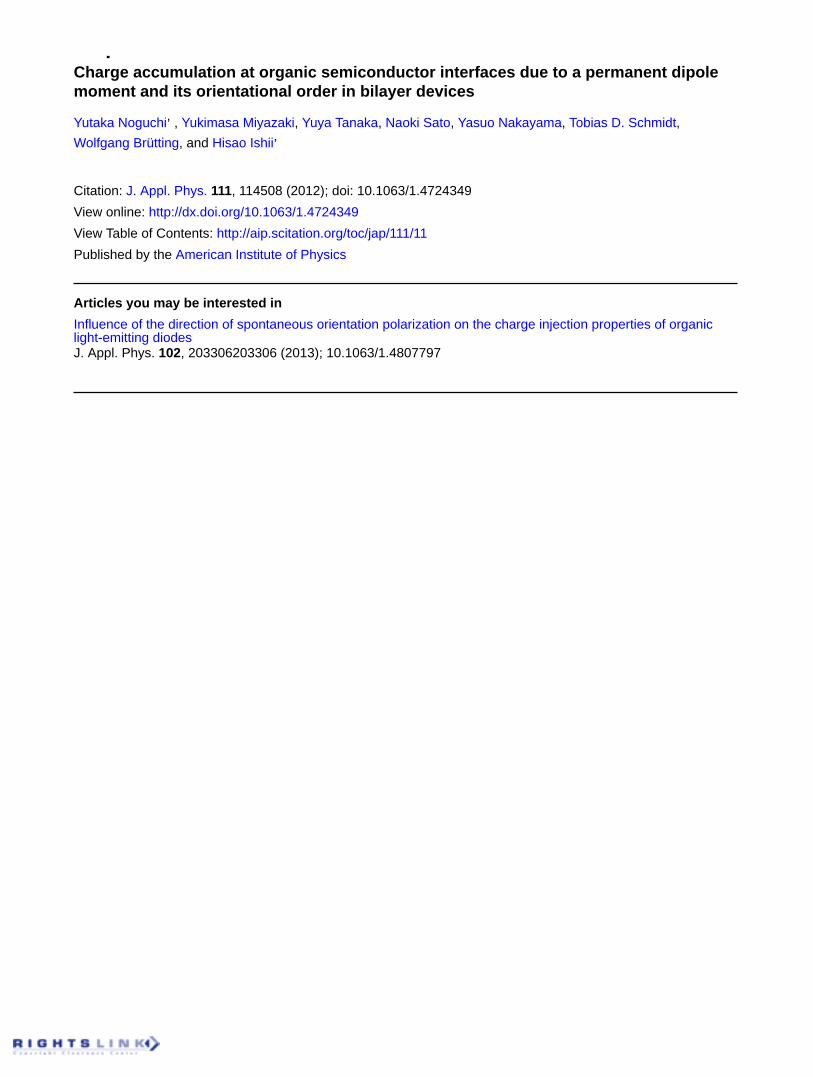
Charge accumulation at organic semiconductor interfaces due to a permanent dipolemoment and its orientational order in bilayer devices
Yutaka Noguchi, , Yukimasa Miyazaki, Yuya Tanaka, Naoki Sato, Yasuo Nakayama, Tobias D. Schmidt,Wolfgang Brütting, and Hisao Ishii,
Citation: J. Appl. Phys. 111, 114508 (2012); doi: 10.1063/1.4724349View online: http://dx.doi.org/10.1063/1.4724349View Table of Contents: http://aip.scitation.org/toc/jap/111/11Published by the American Institute of Physics
Articles you may be interested inInfluence of the direction of spontaneous orientation polarization on the charge injection properties of organiclight-emitting diodesJ. Appl. Phys. 102, 203306203306 (2013); 10.1063/1.4807797
Charge accumulation at organic semiconductor interfaces due to apermanent dipole moment and its orientational order in bilayer devices
Yutaka Noguchi,1,2,3,a) Yukimasa Miyazaki,2 Yuya Tanaka,2 Naoki Sato,2 Yasuo Nakayama,1
Tobias D. Schmidt,4 Wolfgang Brutting,4 and Hisao Ishii1,2,b)
1Center for Frontier Science, Chiba University, 1-33 Yayoi-cho, Inage, Chiba 263-8522, Japan2Graduate School of Advanced Integration Science, Chiba University, 1-33 Yayoi-cho, Inage-ku,Chiba 263-8522, Japan3PRESTO, Japan Science and Technology Agency, 4-1-8 Honcho Kawaguchi, Saitama 332-0012, Japan4Institute of Physics, University of Augsburg, Augsburg 86159, Germany
(Received 21 March 2012; accepted 30 April 2012; published online 5 June 2012)
Charge accumulation at the organic heterointerfaces in multilayer organic light-emitting diodes
(OLEDs) is an important process for understanding their device operation, efficiency, and degradation
properties. Charge accumulation behavior has typically been analyzed in terms of the energy barrier
and difference of the charge carrier mobility across heterointerfaces. In this study, we demonstrate that
permanent dipole moments and their orientational order also play a significant role in the charge
behavior at organic semiconductor interfaces. The charge accumulation properties of bilayer devices
composed of polar or nonpolar molecules deposited on a 4,4’-bis[N-(1-naphthyl)-N-phenylamino]
-biphenyl layer between the anode and cathode were examined by displacement current measurement
and impedance spectroscopy. In addition, Kelvin probe measurements for the corresponding bilayer
structures excluding the cathode were performed to analyze the relationship between the potential
profile and charge accumulation properties of the bilayer devices. We found that several polar
molecules including tris-(8-hydroxyquinolate) aluminum, 1,3,5-tris(1-phenyl-1 H-benzimidazol-2-yl)
benzene, 2,9-dimethyl-4,7-diphenyl-1,10-phenanthroline (BCP), and 1,3-bis[2-(4-tert-butylphenyl)-1,
3,4-oxadiazo-5-yl]benzene (OXD-7) are spontaneously ordered in evaporated films, and orientation
polarization remains in bilayer devices. Orientation polarization leads to interface charge which
determines the least amount of accumulated charge in the device under operation. The estimated
interface charge density for these molecules ranged from �2.3 (OXD-7) to �0.5 (BCP) mC/m2.
Furthermore, impedance spectroscopy revealed that the presence of a permanent dipole moment can
suppress the charge dispersion along the interface probably owing to the microscopic potential
fluctuation formed in the vicinity of the interface. These results indicate that the permanent dipole
moment and orientation polarization contribute to the efficient charge accumulation at organic
heterointerfaces and are important parameters for understanding and controlling the charge carrier
dynamics in multilayer OLEDs. VC 2012 American Institute of Physics.
[http://dx.doi.org/10.1063/1.4724349]
I. INTRODUCTION
Charge accumulation behavior at organic heterointerfa-
ces in multilayer organic light-emitting diodes (OLEDs) has
been extensively studied using various experimental meth-
ods and theoretical models, because understanding their
behavior is essential for improving device performance.1–6
Accumulated charges can serve to tune the electric field dis-
tribution to achieve better charge balance. Moreover, accu-
mulated charges in the emission layer of OLEDs increase
the probability of exciton formation, thus, leading to better
efficiency.1,2 However, in tris-(8-hydroxyquinolate) alumi-
num (Alq3)-based OLEDs, the charged molecules accumu-
lated near the emission region can also act as exciton
quenchers,6,7 and the presence of the Alq3 and 4,40-bis
[N-(1-naphthyl)-N-phenylamino]-biphenyl (a-NPD) cation
species is considered responsible for device degradation.8,9
Therefore, detailed understanding of charge accumulation
behavior is required to develop highly efficient multilayer
OLEDs with appropriately constructed interfaces.
Four elements related to charge accumulation in multi-
layer OLEDs should be considered: (i) energy barrier, (ii)
mobility mismatch, (iii) charge recombination ratio, and (iv)
space charge.2,10 Here, the space charge includes real and
polarization charges. Polarization charges are typically
induced by external electric fields and commonly appear as
the dielectric constant in the device parameter. In addition, if
a device contains polar molecules, contributions from their
permanent dipole moments should be considered. In fact,
numerous molecules used in organic semiconductor devices
possess a permanent dipole moment, and the effects of the
dipole moment have been studied in terms of the charge
transport properties of amorphous films containing such po-
lar molecules. The presence of dipolar disorder leads to
lower carrier mobility in a film because dipole moments
induce different local electric fields and thus increase the
width of density of states.11,12 A similar effect has been
a)Electronic mail: [email protected])Electronic mail: [email protected].
0021-8979/2012/111(11)/114508/10/$30.00 VC 2012 American Institute of Physics111, 114508-1
JOURNAL OF APPLIED PHYSICS 111, 114508 (2012)
reported in the transport properties of organic field effect
transistors (OFETs), in which the dipolar disorder in the gate
dielectric material results in lower charge carrier mobility of
the adjacent organic semiconductor film.13–15 In addition to
these effects of individual dipole moments, contributions
from their assembly, such as orientation polarization in a
film, are essential for the comprehensive understanding of
charge accumulation properties; however, compared to other
parameters, they have not been studied sufficiently.
Recently, we proposed that interface charge in an
Alq3-based OLED originates from the orientation polarization
in the Alq3 film.16 Interface charge was first detected by Brut-
ting et al. at the a-NPD/Alq3 interface in the bilayer
OLED.5,17 They found that the hole injection voltage (Vinj) of
these devices appears lower than the built-in voltage (Vbi),
and it shifts to the negative side with increasing Alq3 film
thickness. This behavior is well explained by assuming a con-
stant amount of negative fixed charge at the a-NPD/Alq3 inter-
face. Interface charge density (rint) was estimated to be ca.
�1.1 mC/m2. The interface charge defines the least amount of
the accumulated charge in the operating device. This is
because charge accumulation occurs at biases below Vbi and
the actual current starts flowing after the compensation of
interface charge by accumulated charge. Moreover, Kondakov
et al. have reported that the apparent rint decreases in propor-
tion to the degradation of luminous efficiency.18 However, the
origin of the interface charge still needs to be clarified.
Ito et al. reported the formation of giant surface potential
(GSP) in an Alq3 film and its decay by light irradiation.19 The
surface potential of an Alq3 film on a Au substrate shows lin-
ear growth with a slope of 50 mV/nm as the film thickness
increases. The surface potential reaches 28 V at 560 nm but
diminishes by light absorption of the Alq3 film. Complemen-
tary studies using optical second harmonic generation (SHG)
revealed that GSP originates from the spontaneous order of
the permanent dipole moment of Alq3.19,20 These results indi-
cate that the Alq3 film has orientation polarization that indu-
ces a constant surface charge of 1.42 mC/m2 on the film
independent of its thickness. This value is similar to rint found
at the a-NPD/Alq3 interface in OLEDs, but the polarity is op-
posite. However, the same amount of negative charge should
exist at the bottom side of the Alq3 film, and this negative
charge should appear at the a-NPD/Alq3 interface in bilayer
OLEDs, where Alq3 is deposited on the a-NPD layer. Because
of the light-induced decay property, it has been believed that
GSP does not persist in the actual device. Furthermore, GSP
has not been studied in terms of device properties; however,
GSP can induce the interface charge, if the orientation polar-
ization persists in the actual OLEDs.
GSP is not a unique property of Alq3 films. It has been
found in films of several compounds such as metal com-
plexes,21 1,3,5-tris(1-phenyl-1 H-benzimidazol-2-yl)benzene
(TPBi),22 and 2,9-dimethyl-4,7-diphenyl-1,10-phenanthroline
(BCP).23 Furthermore, the presence of interface charge
has also been suggested at the a-NPD/1,3-bis[2-(4-tert-
butylphenyl)-1,3,4-oxadiazo-5-yl]benzene (OXD-7) inter-
face.17 Kondakov et al. reported voltammetry data for several
devices in which charge injection voltage appears at the
reverse biasing voltages, suggesting the presence of interface
charge.24,25 These studies imply that interface charge and
GSP can exist even in common OLEDs; however, a direct
comparison between interface charge and GSP has not yet
been demonstrated. Clarifying the role of polarization charge
for the charge accumulation properties of a device is essential
for a more accurate understanding and control of device
properties.
In this study, we performed displacement current meas-
urements (DCMs) for bilayer devices consisting of a-NPD
and several kinds of polar or nonpolar molecular layers, and
Kelvin probe (KP) measurements for the corresponding
bilayer structures for a quantitative comparison between inter-
face charge density and GSP intensity. We found that films
composed of polar molecules exhibit GSP behavior and inter-
face charge appears in devices containing such films; how-
ever, neither GSP nor interface charge appears in devices with
films composed of nonpolar molecules. These experimental
results strongly suggest that orientation polarization induces
interface charge in bilayer devices. In addition, we examined
the charge behavior at the interface in bilayer devices using
impedance spectroscopy (IS) and found that the presence of a
permanent dipole moment in the vicinity of an organic hetero-
interface suppresses the charge spreading along the interface.
This behavior can be explained by the microscopic potential
fluctuation due to the dipole moment in the adjacent film. Our
results clearly demonstrate that the permanent dipole moment
of a molecule and its orientational order in the evaporated
film are important factors for understanding and controlling
the charge accumulation properties of a device.
II. METHODS
DCM is a type of capacitance-voltage (C-V) measure-
ment that uses a triangular wave form as the applied voltage
and measures both actual and displacement current responses
(iact and idis). When the sweep rate of the applied triangular
voltage (dV=dt) is sufficiently slow compared to the transient
response of charges in the device (at the quasi-static limit),
the measured current (iDCM) can be expressed as in10,26
iDCM ¼ iact þ Capp
dV
dt; (1)
where Capp is the apparent capacitance of the device. Capp
directly provides information regarding the charge injection/
extraction and accumulation properties of a device. Figure
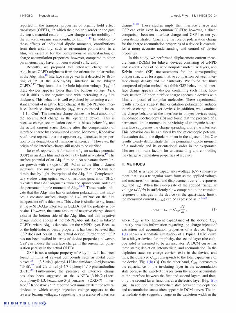
1(a) shows a schematic illustration of a typical DCM curve
for a bilayer device; for simplicity, the second layer (the cath-
ode side) is assumed to be an insulator. A DCM curve has
three states; depletion, intermediate, and accumulation. In the
depletion state, no charge carriers exist in the device, and
thus, the observed Capp corresponds to the total capacitance of
the device [Fig. 1(b) (i)]. On the other hand, Capp increases to
the capacitance of the insulating layer in the accumulation
state because the injected charges from the anode accumulate
at the interface between the first and second layers, and then,
only the second layer functions as a dielectric layer [Fig. 1(b)
(iii)]. In addition, an intermediate state between the depletion
and accumulation states often appears in DCM curves. The in-
termediate state suggests change in the depletion width in the
114508-2 Noguchi et al. J. Appl. Phys. 111, 114508 (2012)
first layer [Fig. 1(b) (ii)], which can originate from the pres-
ence of intentional or unintentional dopants and the charge
filling process of gap states. Here, we define the onset of
charge injection from the electrode, Vinj, and accumulation at
the interface, Vacc, as the intersection of the lines extending
from each state, as shown in Fig. 1(a).
The interface charge density of bilayer devices can be
evaluated by the DCM technique.27,28 If negative interface
charge exists in a bilayer device, hole injection occurs at
biases lower than the threshold voltage of the actual current
(Vth). In this bias range, the second layer acts as an insulator;
in other words, no charges cross the interface. Therefore, the
energy barrier and mobility mismatch at the interface are not
responsible for the amount of accumulated charge. Hole
injection starts at Vinj and the injected holes penetrate into
the first layer through the intermediate state. At Vacc, the
injected holes reach the heterointerface and accumulate until
the negative interface charge has been compensated.17 Thus,
rint can be obtained as
�rintðDCMÞ ¼ðVth
Vacc
CappdV: (2)
Although quasi-static DCM is similar to conventional C-Vmeasurement, DCM detects both injected and extracted
charge carriers and hence can obtain the amount of trapped
charge as well as polarization switching in a device. This is
because the true current (not the root mean square) is meas-
ured as a function of time and applied voltage. The details of
this technique are described elsewhere.10,26
In addition, we measured the surface potential of the
bilayer structure by the KP method to examine the correla-
tions between GSP and interface charge. The observation of
GSP strongly suggests the presence of orientation polariza-
tion in the film and rint can also be evaluated from the thick-
ness dependence of GSP. According to the principle of
electric flux density continuity, the interface charge density
between films 1 and 2 is given by
rintðGSPÞ ¼ �1
d
dxU1 � �2
d
dxU2; (3)
where �n and Un (n ¼ 1; 2) are the dielectric constant and
surface potential of the film n, respectively, and the x axis
corresponds to the surface normal. Here, the real and polar-
ization charges can be the origin of rint. Because GSP is pro-
portional to film thickness, the product of the GSP slope and
dielectric constant gives us interface charge density.
The charge carrier behavior at organic heterointerfaces
was examined using IS and analyzed by C-V and
capacitance-frequency (C-f) curves.29 In these measurements,
an alternating voltage modulation (VACej2pft) superimposed
on a steady-state offset (VDC) is applied to the device and the
ac response including amplitude (iAC) and phase shift (/) are
measured with respect to the applied ac modulation. Because
the equivalent circuit of OLEDs can typically be described as
a parallel circuit of resistance and capacitance, the capaci-
tance at a given VDC and f is derived as
Cð f Þ ¼ � 1
2pf
Z00
jZj2; (4)
where
Z ¼ Z0e�j/ ¼ Z0 þ jZ00 and Z0 ¼VAC
iAC
:
The C-V (C-f) curves at a given f (VDC) were measured by
scanning VDC (f).
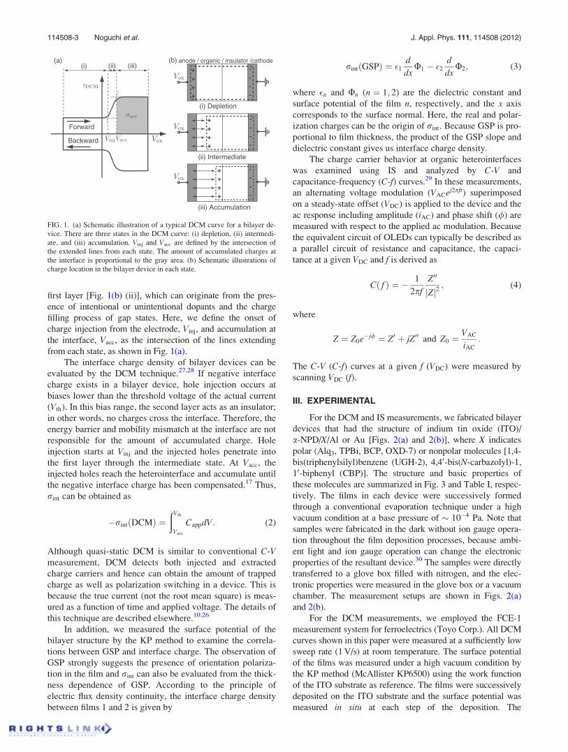
III. EXPERIMENTAL
For the DCM and IS measurements, we fabricated bilayer
devices that had the structure of indium tin oxide (ITO)/
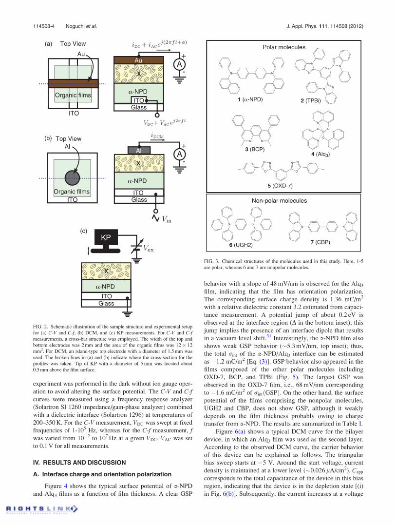
a-NPD/X/Al or Au [Figs. 2(a) and 2(b)], where X indicates
polar (Alq3, TPBi, BCP, OXD-7) or nonpolar molecules [1,4-
bis(triphenylsilyl)benzene (UGH-2), 4,40-bis(N-carbazolyl)-1,
10-biphenyl (CBP)]. The structure and basic properties of
these molecules are summarized in Fig. 3 and Table I, respec-
tively. The films in each device were successively formed
through a conventional evaporation technique under a high
vacuum condition at a base pressure of � 10�4 Pa. Note that
samples were fabricated in the dark without ion gauge opera-
tion throughout the film deposition processes, because ambi-
ent light and ion gauge operation can change the electronic
properties of the resultant device.30 The samples were directly
transferred to a glove box filled with nitrogen, and the elec-
tronic properties were measured in the glove box or a vacuum
chamber. The measurement setups are shown in Figs. 2(a)
and 2(b).
For the DCM measurements, we employed the FCE-1
measurement system for ferroelectrics (Toyo Corp.). All DCM
curves shown in this paper were measured at a sufficiently low
sweep rate (1 V/s) at room temperature. The surface potential
of the films was measured under a high vacuum condition by
the KP method (McAllister KP6500) using the work function
of the ITO substrate as reference. The films were successively
deposited on the ITO substrate and the surface potential was
measured in situ at each step of the deposition. The
FIG. 1. (a) Schematic illustration of a typical DCM curve for a bilayer de-
vice. There are three states in the DCM curve: (i) depletion, (ii) intermedi-
ate, and (iii) accumulation. Vinj and Vacc are defined by the intersection of
the extended lines from each state. The amount of accumulated charges at
the interface is proportional to the gray area. (b) Schematic illustrations of
charge location in the bilayer device in each state.
114508-3 Noguchi et al. J. Appl. Phys. 111, 114508 (2012)
experiment was performed in the dark without ion gauge oper-
ation to avoid altering the surface potential. The C-V and C-fcurves were measured using a frequency response analyzer
(Solartron SI 1260 impedance/gain-phase analyzer) combined
with a dielectric interface (Solartron 1296) at temperatures of
200–350 K. For the C-V measurement, VDC was swept at fixed
frequencies of 1-105 Hz, whereas for the C-f measurement, fwas varied from 10�2 to 107 Hz at a given VDC. VAC was set
to 0.1 V for all measurements.
IV. RESULTS AND DISCUSSION
A. Interface charge and orientation polarization
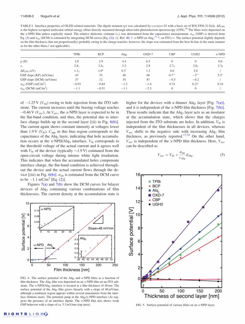
Figure 4 shows the typical surface potential of a-NPD
and Alq3 films as a function of film thickness. A clear GSP
behavior with a slope of 48 mV/nm is observed for the Alq3
film, indicating that the film has orientation polarization.
The corresponding surface charge density is 1.36 mC/m2
with a relative dielectric constant 3.2 estimated from capaci-
tance measurement. A potential jump of about 0.2 eV is
observed at the interface region (D in the bottom inset); this
jump implies the presence of an interface dipole that results
in a vacuum level shift.31 Interestingly, the a-NPD film also
shows weak GSP behavior (�5.3 mV/nm, top inset); thus,
the total rint of the a-NPD/Alq3 interface can be estimated
as �1.2 mC/m2 [Eq. (3)]. GSP behavior also appeared in the
films composed of the other polar molecules including
OXD-7, BCP, and TPBi (Fig. 5). The largest GSP was
observed in the OXD-7 film, i.e., 68 mV/nm corresponding
to �1.6 mC/m2 of rintðGSPÞ. On the other hand, the surface
potential of the films comprising the nonpolar molecules,
UGH2 and CBP, does not show GSP, although it weakly
depends on the film thickness probably owing to charge
transfer from a-NPD. The results are summarized in Table I.
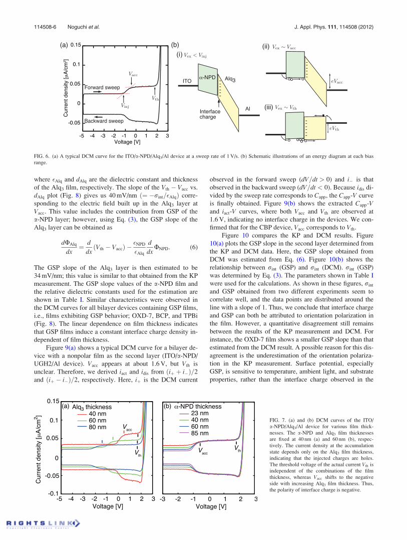
Figure 6(a) shows a typical DCM curve for the bilayer
device, in which an Alq3 film was used as the second layer.
According to the observed DCM curve, the carrier behavior
of this device can be explained as follows. The triangular
bias sweep starts at �5 V. Around the start voltage, current
density is maintained at a lower level (�0.026 lA/cm2). Capp
corresponds to the total capacitance of the device in this bias
region, indicating that the device is in the depletion state [(i)
in Fig. 6(b)]. Subsequently, the current increases at a voltage
FIG. 2. Schematic illustration of the sample structure and experimental setup
for (a) C-V and C-f, (b) DCM, and (c) KP measurements. For C-V and C-fmeasurements, a cross-bar structure was employed. The width of the top and
bottom electrodes was 2 mm and the area of the organic films was 12� 12
mm2. For DCM, an island-type top electrode with a diameter of 1.5 mm was
used. The broken lines in (a) and (b) indicate where the cross-section for the
profiles was taken. Tip of KP with a diameter of 5 mm was located about
0.5 mm above the film surface.
FIG. 3. Chemical structures of the molecules used in this study. Here, 1-5
are polar, whereas 6 and 7 are nonpolar molecules.
114508-4 Noguchi et al. J. Appl. Phys. 111, 114508 (2012)
of �1.25 V (Vinj) owing to hole injection from the ITO sub-
strate. The current increases until the biasing voltage reaches
�0.46 V (Vacc). At Vacc, the a-NPD layer is expected to be in
the flat-band condition, and thus, the potential due to inter-
face charge builds up in the second layer [(ii) in Fig. 6(b)].
The current again shows constant intensity at voltages lower
than 1.9 V (Vth). Capp in this bias region corresponds to the
capacitance of the Alq3 layer, indicating that hole accumula-
tion occurs at the a-NPD/Alq3 interface. Vth corresponds to
the threshold voltage of the actual current and it agrees well
with Vbi of the device (typically �1.9 V) estimated from the
open-circuit voltage during intense white light irradiation.
This indicates that when the accumulated holes compensate
interface charge, the flat-band condition is achieved through-
out the device and the actual current flows through the de-
vice [(iii) in Fig. 6(b)]. rint is estimated from the DCM curve
to be �1.1 mC/m2 [Eq. (2)].
Figures 7(a) and 7(b) show the DCM curves for bilayer
devices of Alq3 containing various combinations of film
thicknesses. The current density at the accumulation state is
higher for the devices with a thinner Alq3 layer [Fig. 7(a)],
and it is independent of the a-NPD film thickness [Fig. 7(b)].
These results indicate that the Alq3 layer acts as an insulator
at the accumulation state, which shows that the charges
injected from the ITO substrate are holes. In addition, Vth is
independent of the film thicknesses in all devices, whereas
Vacc shifts to the negative side with increasing Alq3 film
thickness, as previously reported.17,32 On the other hand,
Vacc is independent of the a-NPD film thickness. Here, Vacc
can be described as
Vacc ¼ Vth þrint
�Alq
dAlq; (5)
TABLE I. Interface properties of OLED-related materials. The dipole moment (p) was calculated by GAUSSIAN 03 with a basis set of B3LYP/6-31 G(d). DEUPS
is the highest occupied molecular orbital energy offset directly measured through ultraviolet photoelectron spectroscopy (UPS).39 The films were deposited on
the a-NPD film unless explicitly stated. The relative dielectric constant (�r) was determined from the capacitance measurement. rint (GSP) is derived from
Eq. (3) and rint (DCM) is estimated by integrating DCM curves [Eq. (2)]. (‡: Ref. 40, †: a-NPD on Alq3,31 *: on ITO,��: The surface potential slightly depends
on the film thickness (but not proportionally) probably owing to the charge transfer; however, the slope was estimated from the best-fit line in the same manner
as for the other films./: not applicable).
TPBi BCP Alq3 OXD-7 CBP UGH2 a-NPD
p (D) 2.0 2.9 4.4 6.5 0 0 0.6
�r 2.87 3.45 3.2 2.9 2.72 2.87 3.35
DEUPS (eV) 1.15 1.0‡ 0.3†
1.3 0.6 2.0 /
GSP slope (KP) (mV/nm) 43 33 48 68 0.7�� �2�� 5.3�
GSP slope (DCM) (mV/nm) 37 12 34 87 �6:5 �6:2 /
rint (GSP) (mC/m2) �0:93 �0:84 �1:2 �1:6 0.74 0.21� 0.16
rint (DCM) (mC/m2) �1:1 �0:51 �1:1 �2:3 0 0 /
FIG. 4. The surface potential of the Alq3 and a-NPD films as a function of
film thickness. The Alq3 film was deposited on an a-NPD film on an ITO sub-
strate. The a-NPD/Alq3 interface is located at a film thickness of 40 nm. The
surface potential of the Alq3 film grows linearly with a slope of 48 mV/nm,
although a nonlinear region appears within several nanometers from the inter-
face (bottom inset). The potential jump at the Alq3/a-NPD interface (D) sug-
gests the presence of an interface dipole. The a-NPD film also shows weak
GSP behavior with a slope of ca. 5.3 mV/nm (top inset). FIG. 5. Surface potential of various films on an a-NPD layer.
114508-5 Noguchi et al. J. Appl. Phys. 111, 114508 (2012)
where �Alq and dAlq are the dielectric constant and thickness
of the Alq3 film, respectively. The slope of the Vth � Vacc vs.
dAlq plot (Fig. 8) gives us 40 mV/nm ð¼ �rint=�AlqÞ corre-
sponding to the electric field built up in the Alq3 layer at
Vacc. This value includes the contribution from GSP of the
a-NPD layer; however, using Eq. (3), the GSP slope of the
Alq3 layer can be obtained as
dUAlq
dx¼ d
dxðVth � VaccÞ �
�NPD
�Alq
d
dxUNPD: (6)
The GSP slope of the Alq3 layer is then estimated to be
34 mV/nm; this value is similar to that obtained from the KP
measurement. The GSP slope values of the a-NPD film and
the relative dielectric constants used for the estimation are
shown in Table I. Similar characteristics were observed in
the DCM curves for all bilayer devices containing GSP films,
i.e., films exhibiting GSP behavior; OXD-7, BCP, and TPBi
(Fig. 8). The linear dependence on film thickness indicates
that GSP films induce a constant interface charge density in-
dependent of film thickness.
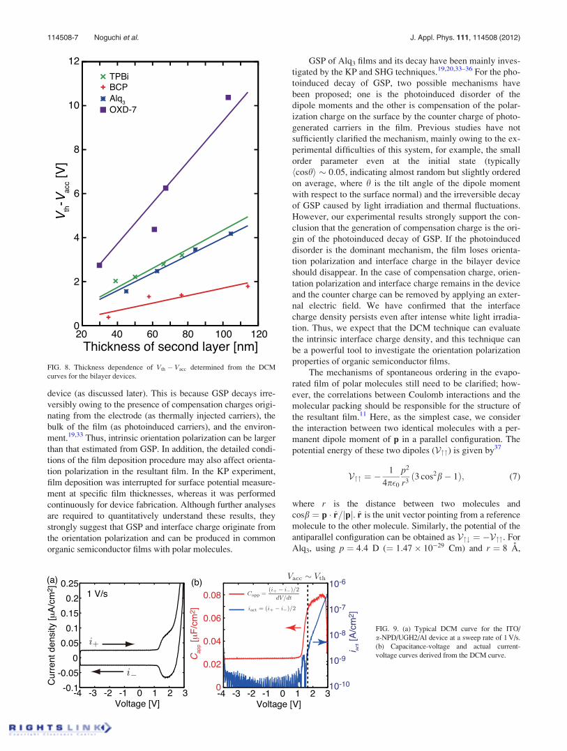
Figure 9(a) shows a typical DCM curve for a bilayer de-
vice with a nonpolar film as the second layer (ITO/a-NPD/
UGH2/Al device). Vacc appears at about 1.6 V, but Vth is
unclear. Therefore, we derived iact and idis from ðiþ þ i�Þ=2
and ðiþ � i�Þ=2, respectively. Here, iþ is the DCM current
observed in the forward sweep (dV=dt > 0) and i� is that
observed in the backward sweep (dV=dt < 0). Because idis di-
vided by the sweep rate corresponds to Capp, the Capp-V curve
is finally obtained. Figure 9(b) shows the extracted Capp-Vand iact-V curves, where both Vacc and Vth are observed at
1.6 V, indicating no interface charge in the devices. We con-
firmed that for the CBP device, Vacc corresponds to Vth.
Figure 10 compares the KP and DCM results. Figure
10(a) plots the GSP slope in the second layer determined from
the KP and DCM data. Here, the GSP slope obtained from
DCM was estimated from Eq. (6). Figure 10(b) shows the
relationship between rint (GSP) and rint (DCM). rint (GSP)
was determined by Eq. (3). The parameters shown in Table I
were used for the calculations. As shown in these figures, rint
and GSP obtained from two different experiments seem to
correlate well, and the data points are distributed around the
line with a slope of 1. Thus, we conclude that interface charge
and GSP can both be attributed to orientation polarization in
the film. However, a quantitative disagreement still remains
between the results of the KP measurement and DCM. For
instance, the OXD-7 film shows a smaller GSP slope than that
estimated from the DCM result. A possible reason for this dis-
agreement is the underestimation of the orientation polariza-
tion in the KP measurement. Surface potential, especially
GSP, is sensitive to temperature, ambient light, and substrate
properties, rather than the interface charge observed in the
FIG. 6. (a) A typical DCM curve for the ITO/a-NPD/Alq3/Al device at a sweep rate of 1 V/s. (b) Schematic illustrations of an energy diagram at each bias
range.
FIG. 7. (a) and (b) DCM curves of the ITO/
a-NPD/Alq3/Al device for various film thick-
nesses. The a-NPD and Alq3 film thicknesses
are fixed at 40 nm (a) and 60 nm (b), respec-
tively. The current density at the accumulation
state depends only on the Alq3 film thickness,
indicating that the injected charges are holes.
The threshold voltage of the actual current Vth is
independent of the combinations of the film
thickness, whereas Vacc shifts to the negative
side with increasing Alq3 film thickness. Thus,
the polarity of interface charge is negative.
114508-6 Noguchi et al. J. Appl. Phys. 111, 114508 (2012)
device (as discussed later). This is because GSP decays irre-
versibly owing to the presence of compensation charges origi-
nating from the electrode (as thermally injected carriers), the
bulk of the film (as photoinduced carriers), and the environ-
ment.19,33 Thus, intrinsic orientation polarization can be larger
than that estimated from GSP. In addition, the detailed condi-
tions of the film deposition procedure may also affect orienta-
tion polarization in the resultant film. In the KP experiment,
film deposition was interrupted for surface potential measure-
ment at specific film thicknesses, whereas it was performed
continuously for device fabrication. Although further analyses
are required to quantitatively understand these results, they
strongly suggest that GSP and interface charge originate from
the orientation polarization and can be produced in common
organic semiconductor films with polar molecules.
GSP of Alq3 films and its decay have been mainly inves-
tigated by the KP and SHG techniques.19,20,33–36 For the pho-
toinduced decay of GSP, two possible mechanisms have
been proposed; one is the photoinduced disorder of the
dipole moments and the other is compensation of the polar-
ization charge on the surface by the counter charge of photo-
generated carriers in the film. Previous studies have not
sufficiently clarified the mechanism, mainly owing to the ex-
perimental difficulties of this system, for example, the small
order parameter even at the initial state (typically
hcoshi � 0:05, indicating almost random but slightly ordered
on average, where h is the tilt angle of the dipole moment
with respect to the surface normal) and the irreversible decay
of GSP caused by light irradiation and thermal fluctuations.
However, our experimental results strongly support the con-
clusion that the generation of compensation charge is the ori-
gin of the photoinduced decay of GSP. If the photoinduced
disorder is the dominant mechanism, the film loses orienta-
tion polarization and interface charge in the bilayer device
should disappear. In the case of compensation charge, orien-
tation polarization and interface charge remains in the device
and the counter charge can be removed by applying an exter-
nal electric field. We have confirmed that the interface
charge density persists even after intense white light irradia-
tion. Thus, we expect that the DCM technique can evaluate
the intrinsic interface charge density, and this technique can
be a powerful tool to investigate the orientation polarization
properties of organic semiconductor films.
The mechanisms of spontaneous ordering in the evapo-
rated film of polar molecules still need to be clarified; how-
ever, the correlations between Coulomb interactions and the
molecular packing should be responsible for the structure of
the resultant film.11 Here, as the simplest case, we consider
the interaction between two identical molecules with a per-
manent dipole moment of p in a parallel configuration. The
potential energy of these two dipoles (V"") is given by37
V"" ¼ �1
4p�0
p2
r3ð3 cos2b� 1Þ; (7)
where r is the distance between two molecules and
cosb ¼ p � r=jpj. r is the unit vector pointing from a reference
molecule to the other molecule. Similarly, the potential of the
antiparallel configuration can be obtained as V"# ¼ �V"". For
Alq3, using p ¼ 4:4 D (¼ 1:47� 10�29 Cm) and r ¼ 8 A,
FIG. 9. (a) Typical DCM curve for the ITO/
a-NPD/UGH2/Al device at a sweep rate of 1 V/s.
(b) Capacitance-voltage and actual current-
voltage curves derived from the DCM curve.
FIG. 8. Thickness dependence of Vth � Vacc determined from the DCM
curves for the bilayer devices.
114508-7 Noguchi et al. J. Appl. Phys. 111, 114508 (2012)
�47:2 meV � V""ð¼ �V"#Þ � 23.6 meV is obtained. Here, ris estimated from the Alq3 film density (1.51 g/cm3). It should
be noted that the parallel configuration takes lower energy on
average compared with the antiparallel configuration. On the
other hand, the thermal energy and the potential energy of
these two configurations are comparable. This implies that the
molecular dipoles can form mostly random but slightly or-
dered configuration in the film phase. Here, we define the mo-
lecular dependent term p2
r3 ¼ m. For Alq3, m can be estimated
as 4:2� 10�31 C2/m. For the other polar molecules used in
this study, appropriate estimation of apparent m value is not
easy because of their anisotropic molecular structures unlike
Alq3. For example, if we calculate m of OXD-7 by assuming
inter-molecular distance simply from its molecular size, mvaries from 10�32 to 10�30 C2/m depending on the combina-
tions of molecular direction. Although the accurate estimation
of film structure is necessary to obtain the m value, it can be
expected to have a similar property (e.g., GSP and interface
charge), if apparent m of the material is � 10�31 C2/m.
B. Charge spreading along the interface
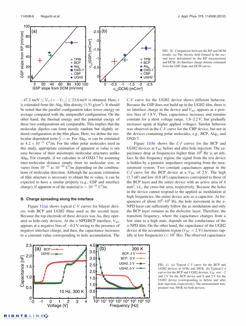
Figure 11(a) shows typical C-V curves for bilayer devi-
ces with BCP and UGH2 films used as the second layer.
Because the top electrode of these devices was Au, they oper-
ated as hole-only devices. At the a-NPD/BCP interface, Vacc
appears at a negative bias of �0.2 V owing to the presence of
negative interface charge, and then, the capacitance increases
to a constant value corresponding to hole accumulation. The
C-V curve for the UGH2 device shows different behavior.
Because the GSP does not build up in the UGH2 film, there is
no interface charge in the device and Vacc appears at a posi-
tive bias of 1.8 V. Then, capacitance increases and remains
constant for a short voltage range, 1.8–2.2 V, but gradually
increases again at higher applied voltages. Similar behavior
was observed in the C-V curve for the CBP device, but not in
the devices containing polar molecules, e.g., BCP, Alq3, and
OXD-7.
Figure 11(b) shows the C-f curves for the BCP and
UGH2 devices at VDC before and after hole injection. The ca-
pacitance drop at frequencies higher than 106 Hz is an arti-
fact. In this frequency region, the signal from the test device
is hidden by a parasitic impedance originating from the mea-
surement system. Two constant capacitances appear in the
C-f curve for the BCP device at a VDC of 2 V. The high
(1.7 nF) and low (0.8 nF) capacitances correspond to those of
the BCP layer and the entire device with an active area of 4
mm2, i.e., the cross-bar area, respectively. Because the holes
in the device cannot respond to the applied ac modulation at
high frequencies, the entire device acts as a capacitor. At fre-
quencies of about 100–104 Hz, the hole movement in the a-
NPD layer can sufficiently follow the ac modulation and only
the BCP layer remains as the dielectric layer. Therefore, the
transition frequency, where the capacitance changes from a
low state to a high state, depends on the conductance of the
a-NPD film. On the other hand, the capacitance of the UGH2
device at the accumulation region (VDC ¼ 2 V) increases rap-
idly at low frequencies (< 102 Hz). The observed capacitance
FIG. 10. Comparison between the KP and DCM
results. (a) The electric field formed in the sec-
ond layer determined by the KP measurement
and DCM. (b) Interface charge density estimated
from the GSP slope and DCM curves.
FIG. 11. (a) Typical C-V curve for the BCP and
UGH2 devices at 10 Hz and 300 K. (b) Typical C-fcurves for the BCP and UGH2 devices. VDC was �2
and 2 V for the BCP device and 0 and 2 V for the
UGH2 device (corresponding to before and after
hole injection, respectively). The measurement tem-
perature was 300 K for both devices.
114508-8 Noguchi et al. J. Appl. Phys. 111, 114508 (2012)
is much higher than that expected from the device geometry.
This capacitance inflation also occurred in the BCP device at
high temperatures (not shown), though the observed fre-
quency is much lower than that in the UGH2 device. In addi-
tion, we measured the C-V and C-f curves for the bilayer
devices containing CBP, Alq3, and OXD-7 films and found
that the capacitance inflation in the nonpolar devices (CBP,
UGH2) appeared at higher frequencies than that in the polar
devices (BCP, Alq3, OXD-7).
Capacitance inflation is likely to occur in bilayer devices
with nonpolar molecules. As shown in Fig. 11(b), the C-fcurve at a bias below the hole injection voltage (�2 V for
the BCP device and 0 V for the UGH2 device) is almost in-
dependent of frequency, indicating that hole injection is nec-
essary for capacitance inflation. Thus, we can eliminate
dielectric dispersion as the origin of this phenomenon. Here,
two other possibilities should be considered; one is the
decrease in the effective thickness of the dielectric layer, and
the other is the expansion of the area that acts as a capacitor.
The former case requires the presence of thermally activated
or injected mobile charges in the bulk region of the second
layer. If thermally activated carriers from the unintended
dopant existed in our devices, capacitance change should be
observed independent of hole injection. Moreover, from the
KP measurements, the UGH2 and CBP films do not show a
significant band bending even at the interface, suggesting
that there are no thermally activated carriers in the films. On
the other hand, a very large energy barrier is formed at the
a-NPD/UGH2 interface (�2 eV, Table I). Because the height
of this energy barrier is the largest among the interfaces used
in this study, compared to the other interfaces, hole injection
beyond this interface is unlikely to occur. Accordingly, the
decrease in the dielectric thickness of the second layer also
cannot explain our experimental results.
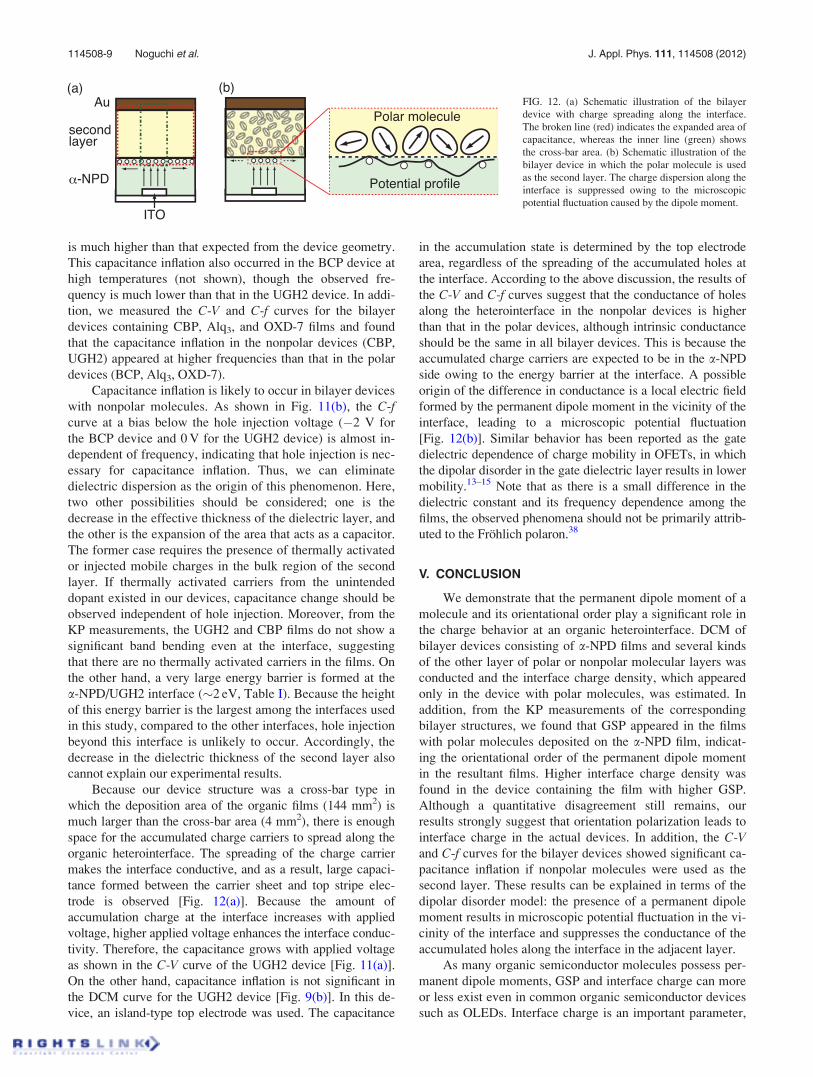
Because our device structure was a cross-bar type in
which the deposition area of the organic films (144 mm2) is
much larger than the cross-bar area (4 mm2), there is enough
space for the accumulated charge carriers to spread along the
organic heterointerface. The spreading of the charge carrier
makes the interface conductive, and as a result, large capaci-
tance formed between the carrier sheet and top stripe elec-
trode is observed [Fig. 12(a)]. Because the amount of
accumulation charge at the interface increases with applied
voltage, higher applied voltage enhances the interface conduc-
tivity. Therefore, the capacitance grows with applied voltage
as shown in the C-V curve of the UGH2 device [Fig. 11(a)].
On the other hand, capacitance inflation is not significant in
the DCM curve for the UGH2 device [Fig. 9(b)]. In this de-
vice, an island-type top electrode was used. The capacitance
in the accumulation state is determined by the top electrode
area, regardless of the spreading of the accumulated holes at
the interface. According to the above discussion, the results of
the C-V and C-f curves suggest that the conductance of holes
along the heterointerface in the nonpolar devices is higher
than that in the polar devices, although intrinsic conductance
should be the same in all bilayer devices. This is because the
accumulated charge carriers are expected to be in the a-NPD
side owing to the energy barrier at the interface. A possible
origin of the difference in conductance is a local electric field
formed by the permanent dipole moment in the vicinity of the
interface, leading to a microscopic potential fluctuation
[Fig. 12(b)]. Similar behavior has been reported as the gate
dielectric dependence of charge mobility in OFETs, in which
the dipolar disorder in the gate dielectric layer results in lower
mobility.13–15 Note that as there is a small difference in the
dielectric constant and its frequency dependence among the
films, the observed phenomena should not be primarily attrib-
uted to the Frohlich polaron.38
V. CONCLUSION
We demonstrate that the permanent dipole moment of a
molecule and its orientational order play a significant role in
the charge behavior at an organic heterointerface. DCM of
bilayer devices consisting of a-NPD films and several kinds
of the other layer of polar or nonpolar molecular layers was
conducted and the interface charge density, which appeared
only in the device with polar molecules, was estimated. In
addition, from the KP measurements of the corresponding
bilayer structures, we found that GSP appeared in the films
with polar molecules deposited on the a-NPD film, indicat-
ing the orientational order of the permanent dipole moment
in the resultant films. Higher interface charge density was
found in the device containing the film with higher GSP.
Although a quantitative disagreement still remains, our
results strongly suggest that orientation polarization leads to
interface charge in the actual devices. In addition, the C-Vand C-f curves for the bilayer devices showed significant ca-
pacitance inflation if nonpolar molecules were used as the
second layer. These results can be explained in terms of the
dipolar disorder model: the presence of a permanent dipole
moment results in microscopic potential fluctuation in the vi-
cinity of the interface and suppresses the conductance of the
accumulated holes along the interface in the adjacent layer.
As many organic semiconductor molecules possess per-
manent dipole moments, GSP and interface charge can more
or less exist even in common organic semiconductor devices
such as OLEDs. Interface charge is an important parameter,
FIG. 12. (a) Schematic illustration of the bilayer
device with charge spreading along the interface.
The broken line (red) indicates the expanded area of
capacitance, whereas the inner line (green) shows
the cross-bar area. (b) Schematic illustration of the
bilayer device in which the polar molecule is used
as the second layer. The charge dispersion along the
interface is suppressed owing to the microscopic
potential fluctuation caused by the dipole moment.
114508-9 Noguchi et al. J. Appl. Phys. 111, 114508 (2012)
because it determines the least amount of accumulated
charge in the operating device, which strongly relates to de-
vice efficiency and degradation. Moreover, the presence of a
permanent dipole moment can suppress the charge spreading
along organic heterointerfaces; thus, making an interface
with polar molecules may lead to an efficient charge recom-
bination and avoid cross-talk between neighboring pixels.
Our results clearly demonstrate that the permanent dipole
moment of the molecule and its orientational order in the
evaporated film are important factors for understanding the
charge accumulation properties of a device.
ACKNOWLEDGMENTS
We would like to thank Dr. H. Fukagawa (NHK) for
useful suggestions for the UGH2 experiments. Y. Noguchi
thanks members of Brutting’s group (Universitat Augsburg)
for their kind cooperation in our experiments. We thank Nip-
pon Steel Chemical Co., Ltd. for providing a-NPD and Alq3
molecules. W.B. would like to thank the Japan Society for
the Promotion of Science (JSPS) for an Invitation Fellowship
for Research in Japan. This research is supported by JSPS
through the “Funding Program for World-Leading Innova-
tive R&D on Science and Technology (FIRST Program)”
initiated by the Council for Science and Technology Policy
(CSTP), the Global-COE Project of Chiba University
(Advanced School for Organic Electronics), and KAKENHI
(Grant Nos. 21245042 and 22750167).
1G. G. Malliaras and J. C. Scott, J. Appl. Phys. 83, 5399 (1998).2B. Ruhstaller, S. A. Carter, S. Barth, H. Riel, W. Riess, and J. C. Scott,
J. Appl. Phys. 89, 4575 (2001).3M. Matsumura, A. Ito, and Y. Miyamae, Appl. Phys. Lett. 75, 1042 (1999).4F. Rohlfing, T. Yamada, and T. Tsutsui, J. Appl. Phys. 86, 4978 (1999).5S. Berleb, W. Brutting, and G. Paasch, Synth. Met. 122, 37 (2001).6T. Haskins, A. Chowdhury, R. H. Young, J. R. Lenhard, A. P. Marchetti,
and L. J. Rothberg, Chem. Mater. 16, 4675 (2004).7R. H. Young, C. W. Tang, and A. P. Marchetti, Appl. Phys. Lett. 80, 874
(2002).8H. Aziz, Z. D. Popovic, N.-X. Hu, A.-M. Hor, and G. Xu, Science 283,
1900 (1999).9D. Y. Kondakov and R. H. Young, J. Appl. Phys. 108, 074513 (2010).
10Y. Noguchi, Y. Tanaka, Y. Miyazaki, N. Sato, Y. Nakayama, and H. Ishii,
in Physics of Organic Semiconductors, edited by W. Brutting and C. Adachi
(Wiley-VCH) (in press).11M. A. Baldo, Z. G. Soos, and S. R. Forrest, Chem. Phys. Lett. 347, 297
(2001).
12M. A. Baldo and S. R. Forrest, Phys. Rev. B 64, 085201 (2001).13J. Veres, S. D. Ogier, S. W. Leeming, D. C. Cupertino, and S. M. Khaffaf,
Adv. Funct. Mater. 13, 199 (2003).14J. Veres, S. Ogier, G. Lloyd, and D. De Leeuw, Chem. Mater. 16, 4543
(2004).15T. Richards, B. Matthew, and H. Sirringhaus, J. Chem. Phys. 128, 234905
(2008).16Y. Noguchi, N. Sato, Y. Tanaka, Y. Nakayama, and H. Ishii, Appl. Phys.
Lett. 92, 203306 (2008).17W. Brutting, S. Berleb, and A. G. Muckl, Org. Electron. 2, 1 (2001).18D. Y. Kondakov, J. R. Sandifer, C. W. Tang, and R. H. Young, J. Appl.
Phys. 93, 1108 (2003).19E. Ito, N. Hayashi, H. Ishii, N. Matsuie, K. Tsuboi, Y. Ouchi, Y. Harima,
K. Yamashita, and K. Seki, J. Appl. Phys. 92, 7306 (2002).20T. Manaka, K. Yoshizaki, and M. Iwamoto, Curr. Appl. Phys. 6, 877
(2006).21N. Hayashi, K. Imai, T. Suzuki, K. Kanai, Y. Ouchi, and K. Seki, in IPAP
Conf. Ser. 6, 69 (2004).22M. Kroger, S. Hamwi, J. Meyer, T. Dobbertin, T. Riedl, W. Kowalsky,
and H. Johannes, Phys. Rev. B 75, 235321 (2007).23N. Kajimoto, Ph.D. dissertation, Tokyo Institute of Technology, 2008.24D. Y. Kondakov, J. Appl. Phys. 99, 024901 (2006).25A. P. Marchetti, K. E. Sassin, R. H. Young, L. J. Rothberg, and D. Y.
Kondakov, J. Appl. Phys. 109, 0137091 (2011).26Y. Tanaka, Y. Noguchi, M. Kraus, W. Brutting, and H. Ishii, Org. Electron.
12, 1560 (2011).27S. Egusa, A. Miura, N. Gemma, and M. Azuma, Jpn. J. Appl. Phys., Part 1
33, 2741 (1994).28S. Ogawa, Y. Kimura, H. Ishii, and M. Niwano, Jpn. J. Appl. Phys., Part 2
42, L1275 (2003).29S. Nowy, W. Ren, A. Elschner, W. Lovenich, and W. Brutting, J. Appl.
Phys. 107, 054501 (2010).30Y. Noguchi, N. Sato, Y. Miyazaki, and H. Ishii, Appl. Phys. Lett. 96,
143305 (2010).31S. T. Lee, Y. M. Wang, X. Y. Hou, and C. W. Tang, Appl. Phys. Lett. 74,
670 (1999).32N. Sato, Y. Noguchi, Y. Tanaka, Y. Nakayama, and H. Ishii, Proc. SPIE
7051, 1S (2008).33K. Yoshizaki, T. Manaka, and M. Iwamoto, J. Appl. Phys. 97, 023703
(2005).34K. Sugi, H. Ishii, Y. Kimura, M. Niwano, E. Ito, Y. Washizu, N. Hayashi,
Y. Ouchi, and K. Seki, Thin Solid Films 464–465, 412 (2004).35N. Kajimoto, T. Manaka, and M. Iwamoto, Jpn. J. Appl. Phys., Part 1 46,
2740 (2007).36K. Ozasa, S. Nemoto, T. Isoshima, E. Ito, M. Maeda, and M. Hara, Appl.
Phys. Lett. 93, 263304 (2008).37M. Schwoerer and H. Wolf, Organic Molecular Solids (Wiley-VCH, 2007).38I. N. Hulea, S. Fratini, H. Xie, C. L. Mulder, N. N. Iossad, G. Rastelli,
S. Ciuchi, and A. F. Morpurgo, Nature Mater. 5, 982 (2006).39Y. Nakayama, S. Machida, Y. Miyazaki, T. Nishi, Y. Noguchi, and
H. Ishii, “Electronic structures at organic heterojunctions of N,N0-bis(1-
naphthyl)-N,N0-diphenyl-1,10-biphenyl-4,40-diamin (NPB)-based organic
light emitting diodes,” (unpublished).40I. G. Hill and A. Kahn, J. Appl. Phys. 86, 2116 (1999).
114508-10 Noguchi et al. J. Appl. Phys. 111, 114508 (2012)