Embed Size (px)
Citation preview
2104195 (1 of 9) © 2021 Wiley-VCH GmbH
www.advmat.de
ReseaRch aRticle
Multifunctional Macroassembled Graphene Nanofilms with High Crystallinity
Li Peng, Ying Han, Meihui Wang, Xiaoxue Cao, Junfeng Gao, Yingjun Liu, Xianjue Chen, Bin Wang, Bo Wang, Chongyang Zhu, Xiao Wang, Ke Cao, Ming Huang, Benjamin V. Cunning, Jintao Pang, Wendao Xu, Yibin Ying, Zhen Xu, Wenzhang Fang,* Yang Lu,* Rodney S. Ruoff,* and Chao Gao*
DOI: 10.1002/adma.202104195
1. Introduction
Graphene-based macroscopic materials, such as fibers, films, and aerogels, have been prepared using graphene oxide (GO) sheets, typically dispersed in water. GO can be readily processed to form micrometer-sized or larger bodies in three dimensions.[1–3] Although great progress has been made in the study and applica-tion of these GO-derived materials in various fields, the products (such as films) do not fully possess the electrical and thermal properties (even with graphitiza-tion at high temperatures) comparable to the ideal properties and some of the realized properties, of graphene itself.[3,4]
A “cooling–contraction” method to separate large-area (up to 4.2 cm in lateral size) graphene oxide (GO)-assembled films (of nanoscale thickness) from substrates is reported. Heat treatment at 3000 °C of such free-standing macroscale films yields highly crystalline “macroassembled graphene nano-films” (nMAGs) with 16–48 nm thickness. These nMAGs present tensile strength of 5.5–11.3 GPa (with ≈3 µm gauge length), electrical conductivity of 1.8–2.1 MS m−1, thermal conductivity of 2027–2820 W m−1 K−1, and carrier relaxation time up to ≈23 ps. As a demonstration application, an nMAG-based sound-generator shows a 30 µs response and sound pressure level of 89 dB at 1 W cm−2. A THz metasurface fabricated from nMAG has a light response of 8.2% for 0.159 W mm−2 and can detect down to 0.01 ppm of glu-cose. The approach provides a straightforward way to form highly crystallized graphene nanofilms from low-cost GO sheets.
The ORCID identification number(s) for the author(s) of this article can be found under https://doi.org/10.1002/adma.202104195.
L. Peng, X. Cao, Y. Liu, Z. Xu, W. Fang, C. GaoMOE Key Laboratory of Macromolecular Synthesis and FunctionalizationDepartment of Polymer Science and EngineeringZhejiang University38 Zheda Road, Hangzhou 310027, P. R. ChinaE-mail: [email protected]; [email protected]. Peng, M. Wang, X. Chen, B. Wang, B. Wang, C. Zhu, M. Huang, B. V. Cunning, R. S. RuoffCenter for Multidimensional Carbon Materials (CMCM)Institute for Basic Science (IBS)Ulsan 44919, Republic of KoreaE-mail: [email protected]. Han, K. Cao, Y. LuDepartment of Mechanical EngineeringCity University of Hong KongKowloon, Hong Kong SAR, P. R. ChinaE-mail: [email protected]. Wang, R. S. RuoffDepartment of ChemistryUlsan National Institute of Science and Technology (UNIST)Ulsan 44919, Republic of KoreaJ. GaoKey Laboratory of Materials Modification by LaserIon and Electron BeamsMinistry of EducationDalian University of TechnologyDalian 116024, P. R. China
X. WangShenzhen Key Laboratory of NanobiomechanicsShenzhen Institutes of Advanced TechnologyChinese Academy of ScienceShenzhen, Guangdong 518055, P. R. ChinaJ. PangThe State Key Laboratory of Fluid Power and Mechatronic SystemsZhejiang UniversityHangzhou 310027, P. R. ChinaW. Xu, Y. YingCollege of Biosystems Engineering and Food ScienceZhejiang University866 Yuhangtang Road, Hangzhou, Zhejiang 310058, P. R. ChinaR. S. RuoffDepartment of Materials Science and EngineeringUlsan National Institute of Science and Technology (UNIST)Ulsan 44919, Republic of KoreaR. S. RuoffSchool of Energy and Chemical EngineeringUlsan National Institute of Science and Technology (UNIST)Ulsan 44919, Republic of Korea
Adv. Mater. 2021, 2104195
© 2021 Wiley-VCH GmbH2104195 (2 of 9)
www.advmat.dewww.advancedsciencenews.com
The mechanical behavior of such macroassembled GO mate-rials, including after “graphitization,” is still under study.[3,5] To achieve high macroscopic strength in graphene-based materials is of practical importance. Bulk graphite is remarkably weak in tension while high-quality centimeter-scale single-layer gra-phene (SLG) films grown by chemical vapor deposition (CVD) can have macroscale tensile fracture strength up to ≈4.5 GPa.[6]
To explore structure–property relations and to try to signifi-cantly improve the performance of macroassembled materials based on GO, free-standing large-area and crystalline building blocks with nanoscale thickness need to be made and studied. If “high strength” can be achieved, such as exceeding that of high strength mass-produced carbon films, paths toward many new applications may be open. Ideally, macroassembled gra-phene nanofilms (nMAGs) could replace metal films whose strong electron–phonon scattering and weak electronic regula-tion could be disadvantageous for certain applications.[7] Free-standing ultrathin films strongly adhere to various substrates when brought them into contact. It is expected to facilitate their integration in high-performance electronic and optoelectronic devices. To the best of our knowledge, the preparation and prop-erties of freely suspended, highly crystalline films composed of stacked and overlapped graphene sheets and with a thickness of tens of nanometers, have not been reported. We have found methods to meet the challenge of preparing free-standing large-area (4.2 cm in diameter) samples with uniform thickness (16–48 nm) and clean surfaces. We suggest our method can be scaled to low-cost and large-area production.
To date it seems that the most common way to produce large-area GO-based nanofilms is through wet assembly fol-lowed by thermal processing; this allows a relatively good con-trol over dimension, chemical composition, and structure.[8] However, the as-assembled nanofilms are not free-standing, but supported by solid substrates or at liquid–air interfaces.[9,10] It limits further modifications of the films such as doping or heating at a very high temperature. This is because most sub-strates have lower thermal endurance than graphene and they may react with the nanofilms at the extremely high tempera-tures that is essential for “graphitization.” Besides, the etchants or polymer transfer agents typically used to transfer nanofilms to various substrates contaminate the films with residues on the surface(s).[11,12] Despite such disadvantages, wet assembly seems to be the best choice for low-cost production of large-area nanofilms with appreciable “quality” for certain applications.
We report here a camphor-assisted “cooling–contraction” strategy to obtain free-standing large-area (4.2 cm in diameter) films with thicknesses ranging from 16 to 48 nm. That we will refer to as “nMAGs.” After heating in an Ar atmosphere to fully carbonize (one might say “graphitize” but we are not literally making graphite) the structure, the nMAGs are found to exhibit outstanding physical properties: tensile fracture strengths up to ≈5.5–11.3 GPa (with sample gauge length of ≈3 µm and width 2–5 µm) and 0.62 ± 0.4 GPa (with a sample gauge length of ≈5 mm and width of ≈1 mm), electrical conductivity in the range 1.8–2.1 MS m−1, and thermal conductivity ranging from 2027 to 2820 W m−1 K−1. The 24 nm nMAG also has a high electron mobility (1770 cm2 V−1 s−1) and long carrier relaxation time of ≈23 ps. Finally, we present the high performances of nMAG-based electronics utilizing the films in thermoacoustic
device (30 µs response time and 89 dB sound pressure level (SPL) at 1 W cm−2) and THz sensor (8.2% light response for 0.159 W mm−2 and sensitivity of 0.01 ppm for glucose as the analyte).
2. Results and Discussion
2.1. Spontaneous Detachment of nMAGs by Contraction during Cooling
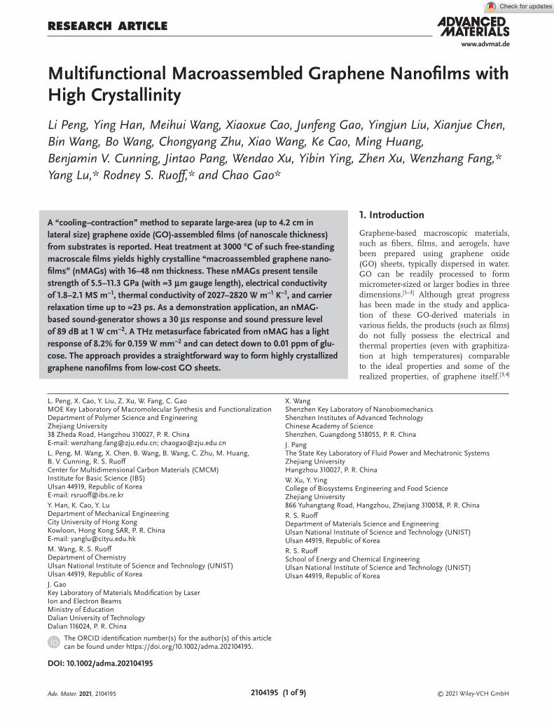
To achieve a robust free-standing nanofilm composed of stacked and overlapped reduced graphene oxide (rGO) sheets (reduction process described further below), it was useful to have: i) a sublimable transfer agent (camphor was used in this work) to enable lifting off the nMAGs, ii) a rigid filter to form a dense film under vacuum and to resist the cooling–contrac-tion bending effect of the transfer agent (we used an anodic aluminum oxide (AAO) filter), and iii) a low areal contact ratio (CR) of the interface between nanofilm and filter. These factors contributed to spontaneous peeling off of the GO film from the AAO filter surface when the deposited camphor/nanofilm cooled down from 120 °C to room temperature.
According to DFT calculations (Figure S1, Supporting Infor-mation), the interfacial binding energy (Eb) of the GO nanofilm to the underlying AAO substrate (Eb-GO/Al2O3
) is higher than that of the nanofilm to camphor (Eb-GO/camphor). In the case of a sufficiently low CR, the nanofilm/camphor membrane interface has greater Eb than the nanofilm/substrate interface (Eb-nanofilm/camphor > Eb-nanofilm/Al2O3
× CR). Under this condition, the contraction occurring during the thermal deposition of poly-crystalline camphor can effectively peel off the nanofilms from rigid AAO filter with a low coefficient of thermal expansion (5.6 × 10⁻⁶ K−1 at room temperature).[13] We thereby obtained free-standing large-area nMAGs after removing camphor by sublimation at 60 °C. Spontaneous peeling avoids contamina-tion and structural damage which are typically encountered when using etchants or polymer transfer agents.
2.2. Preparation of Free-Standing nMAGs
Figure 1a and Figure S2 in the Supporting Information illus-trate the process of nMAG preparation. To obtain rGO films, we vaccum-filtered the GO dispersion followed by deoxygenation at 60 °C in hydroiodic acid aqueous (HI (aq)) vapor. The resulting rGO nanofilm was then detached from the AAO filter by taking advantage of the contraction effect of a camphor film during rapid cooling (Step II). The free-standing nanofilm was then annealed at 3000 °C (Step III) to obtain highly-crystalline nMAG. Notably, the as-prepared free-standing rGO films and nMAGs (4.2 cm in diameter determined by the size of the filter) were robust and could be handled and transferred using tweezers.
The CR was found to be important for the successful delami-nation. We learned that a commercial AAO filter (200 nm pore size; Figure S3, Supporting Information) with a 60% surface porosity worked well. The inhomogeneous spatial chemical vapor reduction of GO nanofilm by HI (aq) gradually reduced the CR of GO/AAO interface. First, the exposure to vapor of HI
Adv. Mater. 2021, 2104195
© 2021 Wiley-VCH GmbH2104195 (3 of 9)
www.advmat.dewww.advancedsciencenews.com
(aq) removed most oxygen-containing functional groups at the interface and thereby, we suggest, reduces Eb (Figure S1, Sup-porting Information).[14] During this deoxygenation process, the exposed side (top surface) of the nanofilm was deoxygenated first after which HI penetrated through the film to reduce GO at the AAO contact interface (Figure 1b; Figure S4a, Supporting Information). This uneven deoxygenation triggered asymmetric shrinkage of rGO film, increasing the stress on the surface exposed to the HI (aq) vapor. We suggest that this stress causes the rGO film to deadhere from the substrate as evidenced by the delamination at the corresponding place where a pinhole was created (Figure S4b,c, Supporting Information). Due to the combined effect of weakened Eb and uneven stress, the area of GO/AAO interface gap was greatly increased by the penetration of vapor from the HI (aq), further reducing the contact area and thus the CR. Finally, a flat stress-free rGO film was obtained on the AAO filter surface (Figure S4d, Supporting Information). At this point, the adhesion at the rGO/AAO interface is consid-erably reduced so that either the osmosis of isopropyl alcohol (Figure S4e, Supporting Information) or cooling of thermally deposited camphor (10–20 mg) can enable detachment in a few seconds (Figure 1c; Video S1, Supporting Information). Notably, the separation of the nanofilm would not occur if an AAO filter with low porosity (<50%) was used (Figure S5, Supporting Information).This is perhaps due to the insufficient penetration of HI at the interface. The premature disappearance of surface stress inhibits the penetration of HI and thus suppresses the expansion of the interface gap.
2.3. Morphology and Crystal Structure of nMAG
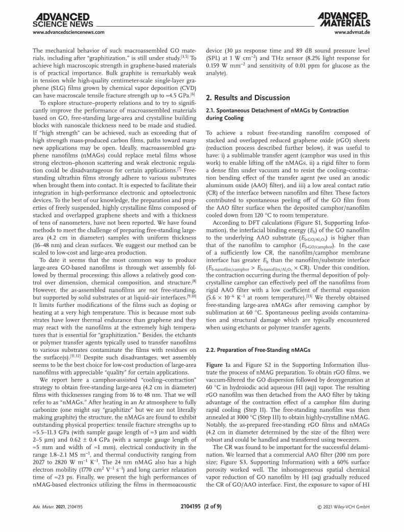
Scanning electron microscopy (SEM) images in Figure 2a and Figure S6a in the Supporting Information show that nMAG has
a smooth surface with a few wrinkles or folds. The decreasing of oxygen peak intensity in X-ray photoelectron spectroscopy (XPS) spectra (531.5 eV; Figure 2b), smaller D peak in Raman spectra (1358.9 cm−1; Figure 2c),[15,16] as well as the upshifting of the (002) peak from 11.6° to 26.5°, and narrowing of the (100) and (110) X-ray diffraction (XRD) peaks (Figure 2d), indicate the annihilation of in-plane defects in graphene by chemical deoxy-genation and thermal graphitization. Besides, the low ID/IG value (<0.5%) and its uniform distribution in the Raman map (inset of Figure 2c) also point to the improved in-plane crystalli-zation of nMAG, typical of long-range planar lattice ordering on the 50 nm scale (Figure 2e; Figure S7, Supporting Information).
The out-of-plane stacking of graphene sheets also recon-struct by the graphitization process. The sharp and symmetric (002) peak (Figure 2d) in the XRD pattern indicates long-range order. The interlayer spacing is 3.36 Å, slightly larger than that in highly oriented pyrolytic graphite (HOPG). We note that the highly aligned (002) lattice fringes and the corresponding sharp fast Fourier transform (FFT) patterns in the transmis-sion electron microscopy (TEM) image (Figure 2f) suggest high crystallinity of nMAGs. No delaminated structures or voids (Figure 2a; Figures S6, S8, and S9, Supporting Informa-tion) were seen throughout the entire cross-section of nMAGs (in the regions we explored, that is). Strong 1010{ } diffrac-tion in the selected-area electron diffraction (SAED) pattern (Figure 2g) indicates that the stacking order is predominantly AB. This is consistent with the well-separated (101) peak and the intense (112) peak in the XRD pattern (Figure 2d). The degree of AB stacking order quantified by the fitted 2D peak in a 100 µm scale Raman mapping is around 96% (Figure 2c).[17] The 2D diffraction patterns in the grazing-incidence wide-angle X-ray scattering (GI-WAXS; Figure 2h) measurements show all the higher-order hkl reflections of nMAG, confirming the high degree of graphitization.
Adv. Mater. 2021, 2104195
Figure 1. Preparation of nMAGs. a) The process to prepare free-standing nMAG. b) Uneven spatial deoxygenation effect of HI (aq) vapor on the two surfaces of the (subsequently) rGO nanofilm at 60 °C in the presence of the AAO substrate (Step I). c) A “cooling–contraction” mechanism acts to separate the rGO film from the AAO substrate (step II: thermal deposition of “hot” camphor on the rGO surface for 1 min at 120 °C, spontaneous separation of nanofilm from AAO by contraction of the camphor film in the air after cooling to 25 °C, followed by removing camphor from the rGO surface of the now separated film (from the AAO filter) by sublimation at 60 °C).
© 2021 Wiley-VCH GmbH2104195 (4 of 9)
www.advmat.dewww.advancedsciencenews.com
We were able to make nMAGs in the range of thicknesses from 16 to 48 nm, by varying the mass loading of the GO sheets dispersion (Figure 2g,h; Figure S8, Supporting Information). We found that the vacuum filtration method results in a spa-tially uniform surface when using a well-dispersed aqueous suspension of GO sheets as the precursor. The histograms of thickness from atomic force microscopy (AFM) images (Figure 2i,j) reveal relatively low roughness of 0.5 nm (16 nm nMAG) and 2.3 nm (48 nm nMAG), consistent with the TEM result (Figure S9, Supporting Information). The diameter of the nMAG is determined by the dimension of the filter and can be varied.
2.4. Mechanical Behavior and Deformation Mechanism of Free-Standing nMAGs
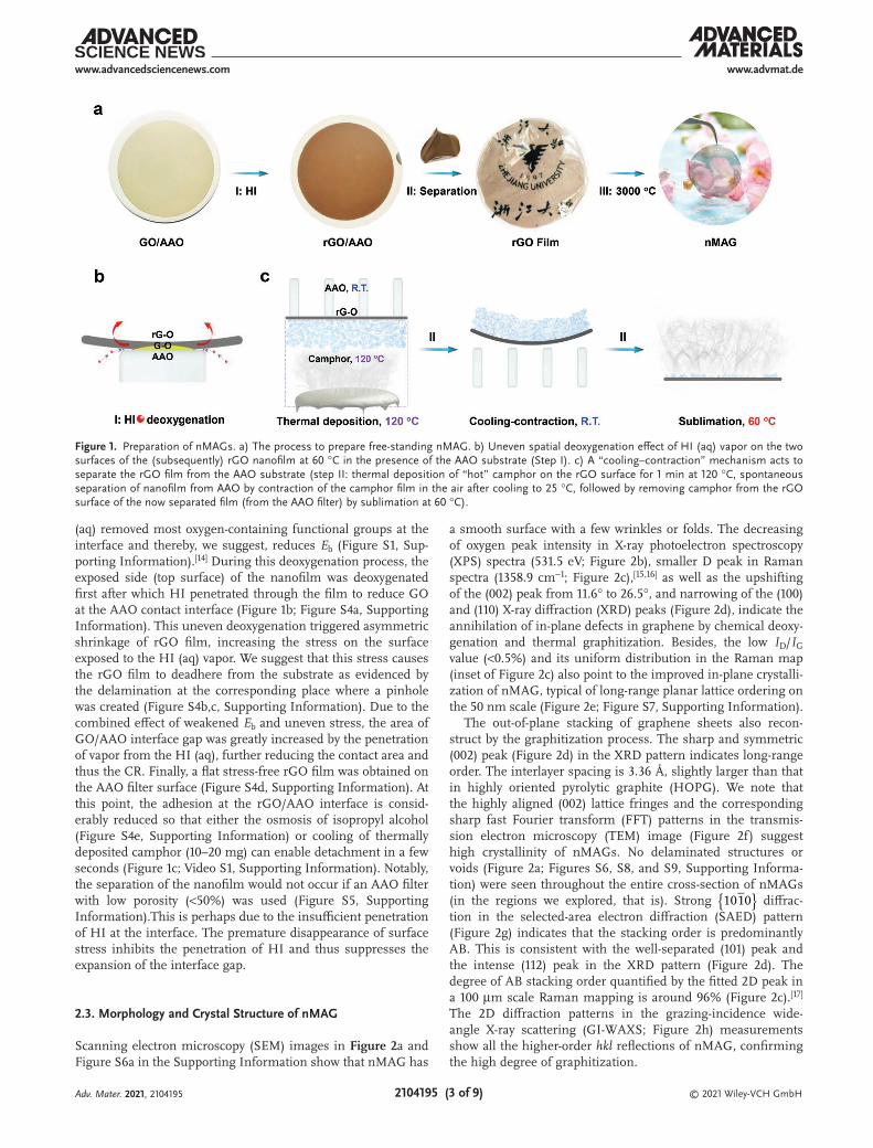
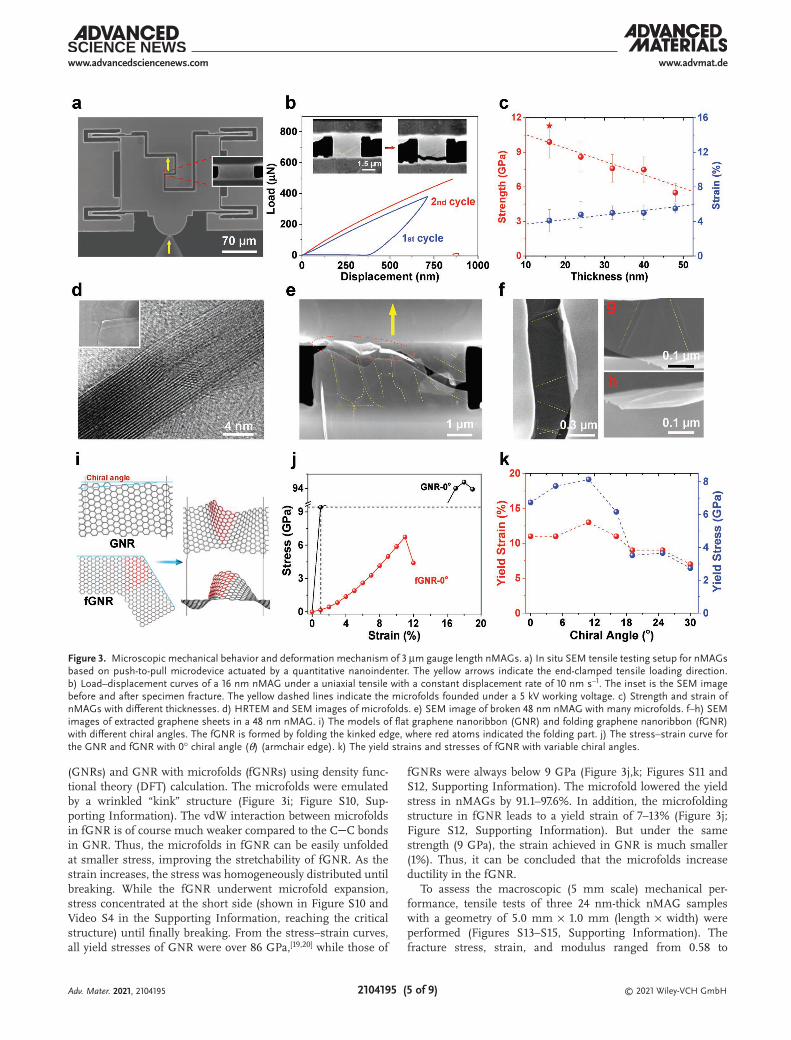
To characterize the microscopic (micrometer-scale) mechan-ical behaviors and fracture mechanism of nMAG samples, we first performed end-clamped tensile tests by using in situ nanomechanical platform equipped with a push-to-pull (PTP) device shown in Figure 3a.[18] Figure 3b shows typical
load–displacement curves measured from a 16 nm-thick nMAG specimen (insets of Figure 3b). As summarized in Figure 3c, the average strength of ≈9.9 GPa and modulus of ≈269 GPa were extracted for these microscale nMAGs, with maximum values up to ≈11.3 and 289 GPa, respectively. Note that the slopes of the second loading curves were larger than the first loading curve, unlike monolayer graphene tested by the same method.[19] It is possibly due to the interfacial sliding and unfolding of microfolds in thicker samples (Figure 3d,e). After the first loading–unloading process, some microfolds were open, which strengthened the nMAGs in the second loading process. Finally, brittle fracture of nMAGs occurred at a strain of 4.1% without a yield stage and the fracture morphology was shown in the inset of Figure 3b, which exhibited obvious crack bifurcation, as recorded by SEM (Video S2, Supporting Infor-mation). With the increase of thickness, the strength of nMAGs decreased from 9.9 GPa (16 nm) to 5.5 GPa (48 nm) and the strain was increased from 4.0% to 5.6% (Figure 3c), which could be due to a greater number of microfolds in thicker films (Figure 3b,e; Note S1, Supporting Information).
To understand the effect of microfold(s) on nMAGs, we simulated the stretching process of flat graphene nanoribbons
Adv. Mater. 2021, 2104195
Figure 2. Structure of nMAG. a) SEM image showing the surface of nMAG (top), and cross-sectional image TEM showing stacked layers in nMAG (48 nm, bottom). b) XPS of GO (O/C ≈ 0.476), rGO (O/C ≈ 0.149), and nMAG (O/C ≈ 0). c) Raman spectra of GO, rGO, and nMAG; Raman maps showing the distribution of ID/IG and (I(2DT)/I(2DT + 2D2)). d) Wide-angle X-ray scattering (transmission mode) spectrum of stacked GO, rGO, and nMAG films (46-layer, thickness ≈ 48 nm per layer). e) STM image of nMAG surface. f) Cross-sectional TEM image of nMAG and the corresponding FFT patterns (inset). g) TEM image of nMAG (thickness, 16 nm) and the corresponding selected area electron diffraction pattern (inset shows SAED). h) 2D synchrotron GI-WAXS patterns of nMAG (thickness 48 nm) on a silicon wafer. i,j) AFM images and plots of nMAGs with 16 and 48 nm thickness.
© 2021 Wiley-VCH GmbH2104195 (5 of 9)
www.advmat.dewww.advancedsciencenews.com
(GNRs) and GNR with microfolds (fGNRs) using density func-tional theory (DFT) calculation. The microfolds were emulated by a wrinkled “kink” structure (Figure 3i; Figure S10, Sup-porting Information). The vdW interaction between microfolds in fGNR is of course much weaker compared to the CC bonds in GNR. Thus, the microfolds in fGNR can be easily unfolded at smaller stress, improving the stretchability of fGNR. As the strain increases, the stress was homogeneously distributed until breaking. While the fGNR underwent microfold expansion, stress concentrated at the short side (shown in Figure S10 and Video S4 in the Supporting Information, reaching the critical structure) until finally breaking. From the stress–strain curves, all yield stresses of GNR were over 86 GPa,[19,20] while those of
fGNRs were always below 9 GPa (Figure 3j,k; Figures S11 and S12, Supporting Information). The microfold lowered the yield stress in nMAGs by 91.1–97.6%. In addition, the microfolding structure in fGNR leads to a yield strain of 7–13% (Figure 3j; Figure S12, Supporting Information). But under the same strength (9 GPa), the strain achieved in GNR is much smaller (1%). Thus, it can be concluded that the microfolds increase ductility in the fGNR.
To assess the macroscopic (5 mm scale) mechanical per-formance, tensile tests of three 24 nm-thick nMAG samples with a geometry of 5.0 mm × 1.0 mm (length × width) were performed (Figures S13–S15, Supporting Information). The fracture stress, strain, and modulus ranged from 0.58 to
Adv. Mater. 2021, 2104195
Figure 3. Microscopic mechanical behavior and deformation mechanism of 3 µm gauge length nMAGs. a) In situ SEM tensile testing setup for nMAGs based on push-to-pull microdevice actuated by a quantitative nanoindenter. The yellow arrows indicate the end-clamped tensile loading direction. b) Load–displacement curves of a 16 nm nMAG under a uniaxial tensile with a constant displacement rate of 10 nm s−1. The inset is the SEM image before and after specimen fracture. The yellow dashed lines indicate the microfolds founded under a 5 kV working voltage. c) Strength and strain of nMAGs with different thicknesses. d) HRTEM and SEM images of microfolds. e) SEM image of broken 48 nm nMAG with many microfolds. f–h) SEM images of extracted graphene sheets in a 48 nm nMAG. i) The models of flat graphene nanoribbon (GNR) and folding graphene nanoribbon (fGNR) with different chiral angles. The fGNR is formed by folding the kinked edge, where red atoms indicated the folding part. j) The stress–strain curve for the GNR and fGNR with 0° chiral angle (θ) (armchair edge). k) The yield strains and stresses of fGNR with variable chiral angles.
© 2021 Wiley-VCH GmbH2104195 (6 of 9)
www.advmat.dewww.advancedsciencenews.com
0.66 GPa, 1.3–1.9%, and 51.2–64.0 GPa (Figure S14, Supporting Information), respectively. The difference of mechanical per-formance between macroscale and microscale samples can be attributed to three main reasons. The size effect is well known and nanoscale samples can approach or exhibit ideal strength.[20] But the strength of macroscale samples typically depends on defects and interfaces.[5,21] Grain boundary (GB) defects in macroscale samples can lower their maximum strain and strength but this would be rare in our microscale samples due to the large grain size (≈60 µm). Another type of defect are the edge defects from the sample fabrication process. We think it is likely that the edge of macroscale samples cut manually could initiate cracks more readily than the more uniform edge achieved by cutting by focused Ion beam (FIB) to generate the microscale samples.
2.5. Thermal and Electronic Applications of nMAGs
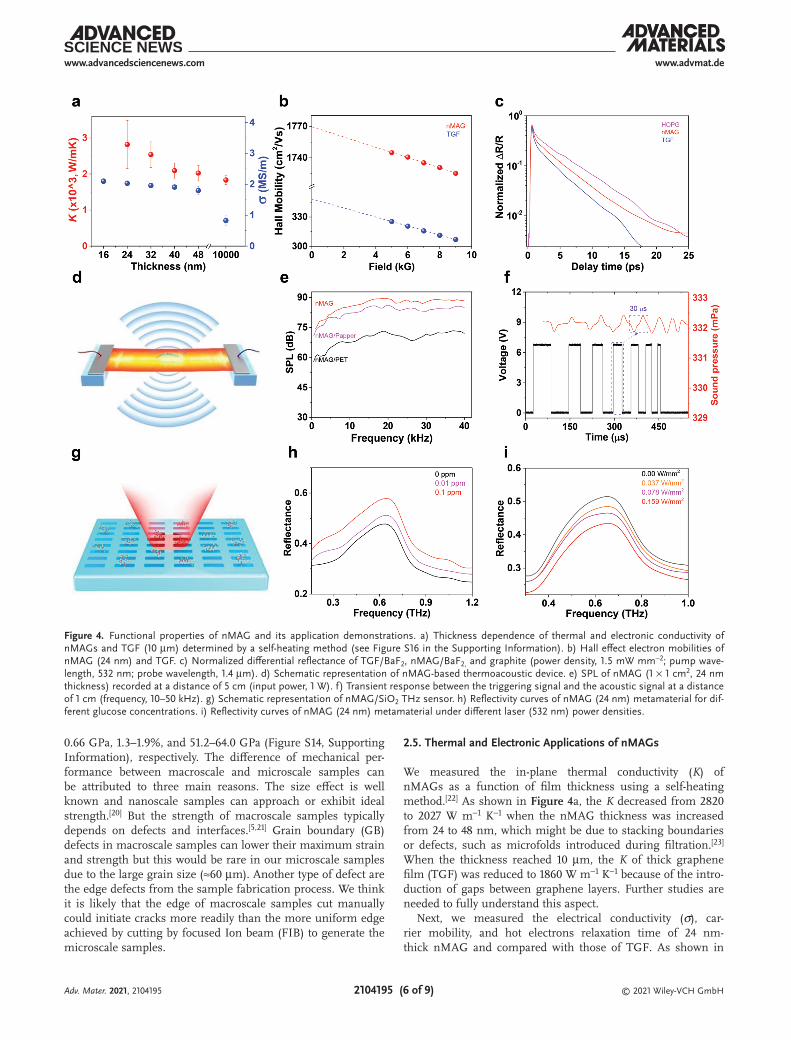
We measured the in-plane thermal conductivity (K) of nMAGs as a function of film thickness using a self-heating method.[22] As shown in Figure 4a, the K decreased from 2820 to 2027 W m−1 K−1 when the nMAG thickness was increased from 24 to 48 nm, which might be due to stacking boundaries or defects, such as microfolds introduced during filtration.[23] When the thickness reached 10 µm, the K of thick graphene film (TGF) was reduced to 1860 W m−1 K−1 because of the intro-duction of gaps between graphene layers. Further studies are needed to fully understand this aspect.
Next, we measured the electrical conductivity (σ), car-rier mobility, and hot electrons relaxation time of 24 nm-thick nMAG and compared with those of TGF. As shown in
Adv. Mater. 2021, 2104195
Figure 4. Functional properties of nMAG and its application demonstrations. a) Thickness dependence of thermal and electronic conductivity of nMAGs and TGF (10 µm) determined by a self-heating method (see Figure S16 in the Supporting Information). b) Hall effect electron mobilities of nMAG (24 nm) and TGF. c) Normalized differential reflectance of TGF/BaF2, nMAG/BaF2, and graphite (power density, 1.5 mW mm−2; pump wave-length, 532 nm; probe wavelength, 1.4 µm). d) Schematic representation of nMAG-based thermoacoustic device. e) SPL of nMAG (1 × 1 cm2, 24 nm thickness) recorded at a distance of 5 cm (input power, 1 W). f) Transient response between the triggering signal and the acoustic signal at a distance of 1 cm (frequency, 10–50 kHz). g) Schematic representation of nMAG/SiO2 THz sensor. h) Reflectivity curves of nMAG (24 nm) metamaterial for dif-ferent glucose concentrations. i) Reflectivity curves of nMAG (24 nm) metamaterial under different laser (532 nm) power densities.
© 2021 Wiley-VCH GmbH2104195 (7 of 9)
www.advmat.dewww.advancedsciencenews.com
Adv. Mater. 2021, 2104195
Figure 4a, nMAG shows a conductivity of 2.1 MS m−1, com-parable to that of the best artificial graphite film and approxi-mately two times higher than the best TGF.[3,24] We attribute the high conductivity of nMAG to its well-stacked structure. Perfect in-plane crystallization of graphene in nMAGs might yield a higher electron density. Meanwhile, large-sized perfect in-plane crystallization, a high degree of out-of-plane crystallization, and the close-stacked structure of nMAGs minimize defect-based and interface-based resistance and act to improve the carrier mobility. For the 48 nm-thick sample, σ is 1.8 MS m−1. The electron mobility of nMAG (24 nm, 1 × 1 mm2 sample) was detected as 1770 cm2 V−1 s−1 (electron density ≈7 × 1019 cm−3), much higher than that of delaminated TGF (348 cm2 V−1 s−1; Figure 4b).
We measured the relaxation time of hot electrons in nMAGs. The graphitic structure weakens carrier-scattering with acoustic phonons in the out-of-plane direction and greatly increases hot carrier lifetime. nMAG and TGF show lifetimes of ≈23 and 17.2 ps (Figure 4c), 1–2 orders of magnitude higher than that of SLG (1 ps) and metals (0.1 ps).[25,26] The relatively lower dif-ferential reflectance (Figure 4c) of nMAG compared to HOPG indicates the presence of boundary defects that act as traps for hot carriers. nMAGs also show enhanced light absorp-tion (26–46%) in the 2.5–10 µm wavelength range (Figure S17, Supporting Information), 10–20 times of SLG (2.3%). This increased absorption coupled with a long lifetime of hot elec-trons implies that nMAGs could be useful in next-generation optoelectronic devices.
Similar to TGFs, nMAGs (24 nm) could be doped by Br2 and MoCl5 without significant structural damage (Figure S18a–c, Supporting Information).[27,28] The Br2- and MoCl5-doped nMAGs show electrical conductivities of 3.7 × 10⁷ and 3.1 × 10⁷ S m−1, respectively (Figure S18d, Sup-porting Information). Assuming a density of 2.37 g cm−3, the specific electrical conductivities of Br2- and MoCl5-doped nMAGs are 1.5 × 10⁴ and 1.3 × 10⁴ S m2 kg−1, respec-tively, approxi mately two times of copper.[29] The increasing/decreasing doping states alter electrical transport mecha-nisms of nMAGs from semiconductor to metallic behavior (Figure S18e, Supporting Information), which is presum-ably due to the overlapping of valence and conduction bands resulting from a shift of the Fermi level.[30]
2.6. nMAG-Based Sound-Generator
We used a 24 nm-thick nMAG as a conductor to fabricate loudspeakers, which work by fast and periodic heating of air (Figure 4d).[31,32] The nMAG (1 × 1 cm2) was self-standing without a supporting substrate (Figure S19, Supporting Infor-mation). An input power of 1 W cm−2 was applied on nMAG under a low voltage of 4.9 V. As shown in Figure 4e, the nMAG film shows a higher SPL of ≈89 dB than that obtained from SLG (<55 dB),[33] and laser-induced graphene (60 dB) under the same input power.[34,35] The high SPL of nMAG is caused by the self-standing state and low heat capacity per unit area, which lowers heat loss to the thermoacoustic system and thus improves the heat transfer efficiency to the surrounding fluid.[33] The decreased SPL of nMAGs from ≈89 to ≈85 dB (paper
substrate) and ≈67 dB (poly(ethylene terephthalate) substrate) confirms the principle above. Besides, the free-standing state and nanoscale thickness improve the thermoacoustic conver-sion speed of nMAG. The nMAG-based sounder-emitter shows a ≈30 µs transient response (Figure 4f; Figure S21, Supporting Information), twice as fast as the best-reported graphene-based sound-emitter till now.[32] Furthermore, the sound pressure of the sound-generator does not decrease during continuous oper-ation for one day due to the good structural stability of nMAGs under thermal shock (fast and periodic heating). As found by TGA (Figure S21, Supporting Information), the nMAG is stable at 450 °C in air without obvious chemical damage and thus weight loss.
2.7. nMAG/SiO2 Heterojunction THz Sensor
As the Fermi level of graphene can be tuned by external mole-cules on its surface, graphene-metamaterial integrated devices show potential in THz sensing.[36,37] We fabricated large-area nMAG (24 nm thick) THz metamaterial by laser engraving technology (Figure 4g). The nMAG metasurface on a quartz substrate (2 mm thick) shows a plasmonic resonance peak at ≈0.65 THz due to its low sheet resistance (20.3 Ω ◻−1) and specific array structure (150 µm × 30 µm), consistent with the simulated result using finite difference time domain (FDTD) method (Figure 4h; Figure S22, Supporting Information). The resonant peak shows a 10.6% shift in amplitude when changing the concentration of glucose from 0 to 0.1 ppm with a max-imum sensitivity of 0.01 ppm.[38,39] nMAG also shows a pho-toelectric effect due to its strong light absorption (Figure S14, Supporting Information) and a long relaxation time of hot elec-trons (Figure 4c). Under laser irradiation, a large number of hot electrons are created in nMAG (Figure 4i), lowering the reflec-tance by 8.2% (0.159 W mm−2). For comparison, this effect is much lower for metals (only 2.5% that of nMAG) because of their strong electron–phonon coupling.[24]
3. Conclusions
We have prepared large-area, free-standing, and highly crystal-line nMAGs of well-controlled thickness (16–48 nm) without using etchants or polymers. The densely stacked nanofilms exhibit physical properties comparable to the CVD-grown high-quality graphene/graphite films, that is, carrier relaxa-tion time of ≈23 ps, carrier mobility of 1770 cm2 V−1 s−1, elec-trical conductivity of 1.8–2.1 MS m−1, thermal conductivity of 2027–2820 W m−1 K−1, and tensile strengths of 5.5–11.3 GPa (≈3 µm gauge length). DFT calculations suggest that in-plane microfolds would affect the mechanical behavior of nMAG considerably. The nMAG was then used as a free-standing sound-emitter which showed an SPL of ≈89 dB and a response time of 30 µs. A sensitive graphene/Si THz heterojunction sensor was also made using this material. This method used to assemble graphene nanofilms could be extended to the fabrica-tion of other 2D material-based nanofilms and heterostructures for potential applications such as high-frequency functional devices. nMAGs can likely be used in high-performance
© 2021 Wiley-VCH GmbH2104195 (8 of 9)
www.advmat.dewww.advancedsciencenews.com
Adv. Mater. 2021, 2104195
electronic and optoelectronic devices that might compete (for certain applications) with SLG, and that might be used in other ways that SLG and thicker macroassembled graphene films cannot be used for.
Supporting InformationSupporting Information is available from the Wiley Online Library or from the author.
AcknowledgementsL.P. and Y.H. contributed equally to this work. L.P., M.W., X.C., B.W., B.W., C.Z., M.H., B.V.C., and R.S.R. acknowledge support from the Institute for Basic Science (IBS-R019-D1); L.P. initiated this work in collaboration with IBS CMCM colleagues while he was a visiting student researcher. This work was also supported by the National Key R&D Program of China (No. 2016YFA0200200), the Fundamental Research Funds for the Central Universities, the National Natural Science Foundation of China (Nos. 52090030, 51703194, 51973191, 51873191, and 21805242), the China Postdoctoral Science Foundation (2020M681819), and the Key Research and Development Plan of Zhejiang Province (2018C01049). Y.H., K.C., and Y.L. acknowledge financial support from the Hong Kong Research Grant Council (RGC) RFS2021-1S05, the City University of Hong Kong SRG 7005234, and the National Natural Science Foundation of China (NSFC) 11922215.
Conflict of InterestThe authors declare no conflict of interest.
Data Availability StatementResearch data are not shared.
Keywordsgraphene nanofilms, high crystallinity, macroassembly, terahertz sensors, thermoacoustic devices
Received: June 20, 2021Revised: August 1, 2021
Published online:
[1] a) H. Sun, Z. Xu, C. Gao, Adv. Mater. 2013, 25, 2554; b) Z. Xu, C. Gao, Nat. Commun. 2011, 2, 571.
[2] a) J. E. Kim, T. H. Han, S. H. Lee, J. Y. Kim, C. W. Ahn, J. M. Yun, S. O. Kim, Angew. Chem., Int. Ed. 2011, 123, 3099; b) U. N. Maiti, J. Lim, K. E. Lee, W. J. Lee, S. O. Kim, Adv. Mater. 2014, 26, 615.
[3] L. Peng, Z. Xu, Z. Liu, Y. Guo, P. Li, C. Gao, Adv. Mater. 2017, 29, 1700589.
[4] a) Y. Hao, L. Wang, Y. Liu, H. Chen, X. Wang, C. Tan, S. Nie, J. W. Suk, T. Jiang, T. Liang, J. Xiao, W. Ye, C. R. Dean, B. I. Yakobson, K. F. McCarty, P. Kim, J. Hone, L. Colombo, R. S. Ruoff, Nat. Nano-technol. 2016, 11, 426; b) A. A. Balandin, Nat. Mater. 2011, 10, 569.
[5] P. Zhang, L. Ma, F. Fan, Z. Zeng, C. Peng, P. E. Loya, Z. Liu, Y. Gong, J. Zhang, X. Zhang, P. M. Ajayan, T. Zhu, J. Lou, Nat. Commun. 2014, 5, 3782.
[6] B. Wang, B. V. Cunning, N. Y. Kim, F. Kargar, S.-Y. Park, Z. Li, S. R. Joshi, L. Peng, V. Modepalli, X. Chen, Y. Shen, W. K. Seong, Y. Kwon, J. Jang, H. Shi, C. Gao, G.-H. Kim, T. J. Shin, K. Kim, J.-Y. Kim, A. A. Balandin, Z. Lee, R. S. Ruoff, Adv. Mater. 2019, 31, 1903039.
[7] B. L. Sharma, Metal-Semiconductor Schottky Barrier Junctions and their Applications, Springer-Verlag, New York 2013, p. 113.
[8] W. Fang, L. Peng, Y. Liu, F. Wang, Z. Xu, C. Gao, Chin. J. Polym. Sci. 2021, 39, 267.
[9] H. Liu, H. Wang, X. Zhang, Adv. Mater. 2015, 27, 249.[10] X. Wang, Z. Xiong, Z. Liu, T. Zhang, Adv. Mater. 2015, 27, 1370.[11] G. Lupina, J. Kitzmann, I. Costina, M. Lukosius, C. Wenger, A. Wolff,
S. Vaziri, M. Östling, I. Pasternak, A. Krajewska, W. Strupinski, S. Kataria, A. Gahoi, M. Lemme, G. Ruhl, G. Zoth, O. Luxenhofer, W. Mehr, ACS Nano 2015, 9, 4776.
[12] X. Wang, A. Dolocan, H. Chou, L. Tao, A. Dick, D. Akinwande, C. Willson, Chem. Mater. 2017, 29, 2033.
[13] C. Lee, J. Choi, S. Qin, Q. Xu, P. Qiao, Z. Shan, W. Hwang, in Fifth Asia International Symposium on Mechatronics (AISM 2015), IEEE, Piscataway, NJ, USA 2015, https://doi.org/10.1049/cp.2015.1588
[14] J. Zhao, S. Pei, W. Ren, L. Gao, H.-M. Cheng, ACS Nano 2010, 4, 5245.
[15] R. Al-Gaashani, A. Najjar, Y. Zakaria, S. Mansour, M. A. Atieh, Ceram. Int. 2019, 45, 14439.
[16] J. Kotakoski, A. V. Krasheninnikov, U. Kaiser, J. C. Meyer, Phys. Rev. Lett. 2011, 106, 105505.
[17] L. G. Cançado, K. Takai, T. Enoki, M. Endo, Y. A. Kim, H. Mizusaki, N. L. Speziali, A. Jorio, M. A. Pimenta, Carbon 2008, 46, 272.
[18] H. Zhang, J. Tersoff, S. Xu, H. Chen, Q. Zhang, K. Zhang, Y. Yang, C.-S. Lee, K.-N. Tu, J. Li, Y. Lu, Sci. Adv. 2016, 2, e1501382.
[19] K. Cao, S. Feng, Y. Han, L. Gao, T. H. Ly, Z. Xu, Y. Lu, Nat. Commun. 2020, 11, 284.
[20] C. Lee, X. Wei, J. W. Kysar, J. Hone, Science 2008, 321, 385.[21] a) S. Jin, B. Chung, H. J. Park, B. V. Cunning, J.-H. Lee, A. Yoon,
M. Huang, H. Seo, D. Lee, Z. Lee, R. S. Ruoff, S. Ryu, Adv. Funct. Mater. 2020, 30, 2005381; b) A. Zandiatashbar, G. H. Lee, S. J. An, S. Lee, N. Mathew, M. Terrones, T. Hayashi, C. R. Picu, J. Hone, N. Koratkar, Nat. Commun. 2014, 5, 3186.
[22] G. Xin, T. Yao, H. Sun, S. M. Scott, D. Shao, G. Wang, J. Lian, Science 2015, 349, 1083.
[23] N. Yang, X. Ni, J.-W. Jiang, B. Li, Appl. Phys. Lett. 2012, 100, 093107.
[24] M. Murakami, A. Tatami, M. Tachibana, Carbon 2019, 145, 23.
[25] M. Massicotte, P. Schmidt, F. Vialla, K. Watanabe, T. Taniguchi, K. J. Tielrooij, F. H. L. Koppens, Nat. Commun. 2016, 7, 12174.
[26] M. T. Mihnev, J. R. Tolsma, C. J. Divin, D. Sun, R. Asgari, M. Polini, C. Berger, W. A. de Heer, A. H. MacDonald, T. B. Norris, Nat. Commun. 2015, 6, 8105.
[27] Y. Liu, M. Yang, K. Pang, F. Wang, Z. Xu, W. Gao, C. Gao, Carbon 2020, 156, 205.
[28] H. Peng, J. Am. Chem. Soc. 2008, 130, 42.[29] Y. Liu, Z. Xu, J. Zhan, P. Li, C. Gao, Adv. Mater. 2016, 28, 7941.[30] N. Jung, N. Kim, S. Jockusch, N. J. Turro, P. Kim, L. Brus, Nano Lett.
2009, 9, 4133.[31] M. Daschewski, R. Boehm, J. Prager, M. Kreutzbruck, A. Harrer,
J. Appl. Phys. 2013, 114, 114903.[32] H. Tian, D. Xie, Y. Yang, T.-L. Ren, Y.-F. Wang, C.-J. Zhou, P.-G. Peng,
L.-G. Wang, L.-T. Liu, Nanoscale 2012, 4, 3345.[33] J. W. Suk, K. Kirk, Y. Hao, N. A. Hall, R. S. Ruoff, Adv. Mater. 2012,
24, 6342.[34] H. Tian, Y.-L. Cui, Y. Yang, D. Xie, T. Ren, in 2014 IEEE 27th
Int. Conf. on Micro Electro Mechanical Systems (MEMS), IEEE, Piscataway, NJ, USA 2014, pp. 556–559, https://doi.org/10.1109/MEMSYS.2014.6765701.

© 2021 Wiley-VCH GmbH2104195 (9 of 9)
www.advmat.dewww.advancedsciencenews.com
Adv. Mater. 2021, 2104195
[35] L.-Q. Tao, H. Tian, Y. Liu, Z.-Y. Ju, Y. Pang, Y.-Q. Chen, D.-Y. Wang, X.-G. Tian, J.-C. Yan, N.-Q. Deng, Y. Yang, T.-L. Ren, Nat. Commun. 2017, 8, 14579.
[36] S.-H. Lee, J.-H. Choe, C. Kim, S. Bae, J.-S. Kim, Q. H. Park, M. SeSeo, Sens. Actuators, B 2020, 310, 127841.
[37] W. Xu, L. Xie, J. Zhu, L. Tang, R. Singh, C. Wang, Y. Ma, H.-T. Chen, Y. Ying, Carbon 2019, 141, 247.
[38] A. Ahmadivand, B. Gerislioglu, R. Ahuja, Y. Kumar Mishra, Mater. Today 2020, 32, 108.
[39] W. Xu, L. Xie, J. Zhu, W. Wang, Z. Ye, Y. Ma, C.-Y. Tsai, S. Chen, Y. Ying, Food Chem. 2017, 218, 330.