Embed Size (px)
Citation preview

SONG ET AL . VOL. XXX ’ NO. XX ’ 000–000 ’ XXXX
www.acsnano.org
A
CXXXX American Chemical Society
Nanoscale Joule Heating andElectromigration Enhanced Ripeningof Silver Nanowire ContactsTze-Bin Song,†,‡ Yu Chen,†,‡ Choong-Heui Chung,†,‡,§ Yang (Michael) Yang,† Brion Bob,†,‡
Hsin-Sheng Duan,†,‡ Gang Li,† King-Ning Tu,†,* Yu Huang,†,‡,* and Yang Yang†,‡,*
†Department of Materials Science and Engineering and ‡California NanoSystems Institute, University of California Los Angeles, Los Angeles, California 90095,United States and §Department of Materials Science and Engineering, Hanbat National University, Daejeon 305-719, Korea
The excellent mechanical, optical,electrical, and thermal properties oflow-dimensional materials,1�4 such as
nanowires (NWs), nanoparticles (NPs), andnanotubes (NTs) have attracted people's at-tention and have been applied to a numberoffields includingoptical electronics,5 energystorage,6 and sensors.7 With the recent de-mand for thin, transparent, conducting filmsand flexible devices, nanomaterials such ascarbon nanotubes,8,9 graviaphene,10,11 andmetallic nanowires12�14 have emerged aspromising alternatives to replace the brittleindium tin oxide (ITO). In particular, silvernanowire (AgNW) networks provide excel-lent transmittance and conductance andthus have been brought forward as a poten-tial candidate for transparent conductors(TCs) in thin film optoelectronic devices,15
such as touch panels, light emitting diodes(LEDs), and solar cells, due to their potentialhigh-throughput, low-cost fabrication, flex-ibility, and solution-processability. However,the high contact resistance between silvernanowires coming from the insulating sur-factant coating of polyvinylpyrrolidone(PVP) and loose contact between individualAgNWs remains a critical issue, making extraprocessing steps necessary in order toachieve low sheet resistance values desirablefor practical applications.16
Many processing techniques have beenreported to address this issue, includingheat treatment (featuring either a highprocessing temperature or long treatmenttime),12 mechanical pressing,17,18 electro-chemical ion exchange,19 vacuum filtration,20
metal-oxide nanoparticle fusing,21,22 and
* Address correspondence [email protected] (K.-N. Tu);[email protected] (Y. Huang);[email protected] (Y. Yang).
Received for review December 23, 2013and accepted February 11, 2014.
Published online10.1021/nn4065567
ABSTRACT Solution-processed metallic nanowire thin film is a
promising candidate to replace traditional indium tin oxide as the
next-generation transparent and flexible electrode. To date how-
ever, the performance of these electrodes is limited by the high
contact resistance between contacting nanowires; so improving the
point contacts between these nanowires remains a major challenge.
Existing methods for reducing the contact resistance require either a
high processing power, long treatment time, or the addition of
chemical reagents, which could lead to increased manufacturing cost and damage the underlying substrate or device. Here, a nanoscale point reaction
process is introduced as a fast and low-power-consumption way to improve the electrical contact properties between metallic nanowires. This is achieved
via current-assisted localized joule heating accompanied by electromigration. Localized joule heating effectively targets the high-resistance contact points
between nanowires, leading to the automatic removal of surface ligands, welding of contacting nanowires, and the reshaping of the contact pathway
between the nanowires to form a more desirable geometry of low resistance for interwire conduction. This result shows the interplay between thermal and
electrical interactions at the highly reactive nanocontacts and highlights the control of the nanoscale reaction as a simple and effective way of turning
individual metallic nanowires into a highly conductive interconnected nanowire network. The temperature of the adjacent device layers can be kept close
to room temperature during the process, making this method especially suitable for use in devices containing thermally sensitive materials such as polymer
solar cells.
KEYWORDS: elecromigration . ripening . joule heating . transparent electrode . silver nanowire . solution process . polymer solar cell
ARTIC
LE

SONG ET AL . VOL. XXX ’ NO. XX ’ 000–000 ’ XXXX
www.acsnano.org
B
plasmonic welding process.23 Some of these methodsrequire the use of high input powers or long treatmentdurations, while others suffer from obvious scalabilityissues and shadow effect or may damage chemicallysensitive substrates. Recent reports demonstrated thatjoule heating can weld platinum wires and carbonnanotubes by precisely controlling the contact geo-metry and current flow between the two wires.24,25
With the forming of point contacts, hot spots can begenerated at the contact point because of the highlocal current density. In this work, passing currentthrough the small contact points between the wireswith residual insulating surface ligands from the che-mical synthesis process successfully generated enoughpower to weld all the contacts of the wires across theentire large-area devices. During this process, electro-migration occurred at the high current density regionsin the nanowire network26 in and near the contactregion, which plays a critical role in determining theelectrical properties of the metallic nanowires networkand therefore is crucial for the future applications ofthe metallic nanowires. This method is easily transfer-able to large-scale AgNW networks, where substantialimprovement in the conductivity of these silver nano-wire network electrodes can be achieved at low tem-peratures and by using only a small amount of inputenergy over the treatment duration of a few seconds.This process enables us to obtain low-resistance AgNWnetworks and employ them as electrodes in devicesthat require relatively gentle processing conditions,such as polymer solar cells, in which an efficiencyenhancement of 20 times is demonstrated in this work.
RESULTS AND DISCUSSION
A schematic diagram of the experimental setup isshown in Figure 1a, with the red dots indicating hotspots for the electrowelding process. The AgNWs wereeither synthesized according to previous reports19 orcommercially available AgNWs. AgNWswere spun-caston a glass substrate (1.5 � 1.2 cm2) patterned withevaporated metal electrodes to form the nanowirenetwork, and a direct current biaswas applied betweenthe electrodes to allow current to flow through thenanowire network. In our experiment, a current limitwas put in place and adjusted to prevent high-currentbreakdown of the network. The AgNW networks werecharacterized by scanning electron microscopy (SEM),spectrophotometry, and current�voltage measure-ments before and after the electric current treatment.SEM images of the AgNW contacts before the elec-
trical current treatment are shown in Figure 1b, and thesharp interface between the two nanowires in contactis clearly visible. After a current treatment at 0.2 A limitwith 25 V compliance voltage for 30 s, different mor-phologies of contacts were formed and characterizedusing the tilt-angle SEM (Figure 1c,d). In the case shownin Figure 1c, the contact was welded and the top wirehad deformed toward the bottom wire. Figure 1dshowed a contact in which only one side of the contactwelded significantly, forming an asymmetric contactmorphology, which is not seen in those welded con-tacts produced by other treatment methods suchas heating and plasmonic welding, which invariablyproduce a symmetric contact shape at the wire�wirecontact. A low-magnification tilted SEM imagewas also
Figure 1. Experimental setup and scanning electronmicroscope (SEM) images before and after electrowelding treatment. (a)Schematic diagram of the experimental setup, with a continuous network of nanowires allowing for the passage of currentbetween twometal electrodes. (b) Tilted (45�) SEM images of the initial silver nanowire contact. (c, d) Nanowire contacts afterthe electrowelding treatment; differentmorphologies of the silver nanowire contacts are observedunder tilted SEM. (e)Widerviewof several nanowire contacts after the passage of current. The arrows indicate the deformation of the nanowire contacts.
ARTIC
LE

SONG ET AL . VOL. XXX ’ NO. XX ’ 000–000 ’ XXXX
www.acsnano.org
C
taken after the treatment (Figure 1e), showing contactmorphologies distinct from those produced by otherprocesses.23 The difference in the symmetry of thecontact morphology indicates that a different joiningmechanism is at work in our point contact treatment.In order to further understand the reaction taking
place at the contacts, an isolated two-wire contactsystem was fabricated, as shown in Figure 2a. Thedirection of the applied current is indicated by redarrows. A 500 ohm resistor was connected to introducea current limit under 0.1 V bias for the structure. Beforecurrent treatment, the resistance of the two-wire de-vice was larger than 1010 ohm due to the large pointcontact resistance. After the current treatment with amaximum current density of around 1.5 � 107 A/cm2,calculated from the maximum current value to thecross section area of the small nanowire, the resistancewas dramatically reduced to 185 ohm, as shown in theI�V curves depicted in Figure 2d. The ratio betweenthe power generated at the contact and within thenanowire can be expressed as Pc/Pw = Rc/Rw, in whichRc and Rw are the two-wire contact resistance andnanowire resistance, respectively. From experimentalresults, Rc þ Rw is larger than 1010 ohm, and we canestimate that the average Rw from AgNW dimensionsshould be around 180 ohm. This results in the
conclusion Rc . Rw, indicating that nearly 100% ofthe heat generation will be localized at the contactwith little heating effect in the bulk of the AgNWs.The contact morphology of the two-wire device wascharacterized from different viewing angles, left (L)and right (R), as shown in Figure 2a, after applying theelectrical current (Figure 2b,c), and the same asym-metric shape of the contact similar to those in thelarger film was observed. The cross-section of thecontact was made using focused ion beam (FIB) andcharacterized with SEM to gain more insight into thecontact formation. As shown in the inset of Figure 2c,the top nanowire deforms around the bottom nano-wire, and the final contact shape formed to favora good electrical connection between the two. It isobserved that in general, the nanowirewith the smallerdiameter of the two tends to take on the majorityof the morphological changes and the most extremechanges took place at the corner of the contact.This process can be simulated using a finite-element
method, showing three stages of reaction takingplace corresponding to our previous observation fromcross-sectional SEM images (Figure 3). The images inFigure 3 show only a quarter of the simulated structureto highlight the current distribution near the contact.In Figure 3a, the point contact between two pristine
Figure 2. Two-wire contact measurement and characterization. (a) SEM image of a two-wire device, with the red arrowsindicating the direction of current flow. (b, c) Tilted (52�) SEM image of the silver nanowire contact from the differentdirections. The diameters of the top nanowire and the bottomone are around 49 and 58 nm, respectively. The reacted contactwas found at the R (right) corner of the silver nanowires. The cross-sectional SEM image of the two silver nanowires contact isshown in the inset of (c), with the majority of deformation clearly concentrated in the upper nanowire. The scale bar of theinset is 50 nm. (d) Current�voltagemeasurements before and after current passing. The current of the pristine device is in thepA region and the post-treatment device is in the μA, as shown.
ARTIC
LE

SONG ET AL . VOL. XXX ’ NO. XX ’ 000–000 ’ XXXX
www.acsnano.org
D
nanowires leads to current concentrating into a rela-tively small volume, and the presence of surfactantssuch as PVPwill result in an even larger heat generationdue to the high current density and high contactresistance. Under these conditions, strong joule heat-ing will occur at the contact. Once enough heat isgenerated at the contact, increased surface and bulkdiffusion of silver atoms will allow for the welding ofthe point contact to achieve a larger contact area.Furthermore, the tendency for the smaller nanowireto preferentially deform (as in Figure 1c) can beexplained by the dependence of free energy onthe diameter of the nanowire. According to Gibbs�Thomson theory, the Gibbs free energy increasessharply with smaller particle dimensions due to anincreased contribution from the Gibbs�Thomsonpotential, ΔG = 2γΩm/r, where γ is the surface energy,Ωm is the volume per atom of investigatedmaterial, andr is the radius of the nanowires. The AgNW with thesmaller diameter is subject to a higher potential energyand is therefore comparatively unstable compared to thelarger wire. With the localized temperature increaseproducedby jouleheating, the silver atoms in the smallerwire will obtain enough thermal energy to diffuserapidly onto and around the other wire. Similar electricalsintering reactions in silver nanoparticles had beenstudied both experimentally and through simulationpreviously.27�29 The reaction can happen on a time scaleof milliseconds with a reaction temperature exceeding100 �C.27 It was established that the surface diffusionactivation energy of noble metal atoms is typically lessthan 1 eV30,31 and the process can happen even at roomtemperature. With the joule heating and the reductionof the surface diffusion activation energy from the highGibbs�Thomson potential, the process can occur ona very short time scale. Eventually, a reacted contact isformed,generally adoptinga shapesimilar to that shownin Figure 3b, which is reflected in the result in Figure 1c.
After the formation of the reacted contact, reducedcontact resistance will allow for increased current flow.However, the current density will not be homogeneousacross the entire contacted region because the contactarea is still smaller than the bulk of the nanowires.Additionally, in order to minimize the distance elec-trons traveled as they travel from one nanowire to theother, current crowding occurred and the currentdensity was substantially higher at the inner cornerof the contact. As shown in Figure 3b, the highestcurrent density region was at the corner of the contactinstead of the center of the contact. This currentcrowding can introduce an enhancement to the localcurrent density up to 1 order of magnitude from thesimulation and previous report.26 In a two-wire contactsystem, average current density was on the order of107 A/cm2, which indicated a current density of around108 A/cm2 at the corner of the contact. Comparingwiththe data from copper interconnect technology, surfacediffusion induced electromigration occurs at the Sidevice operation temperature of 100 �C with a currentdensity of 106 A/cm2. The melting temperatures ofsilver and copper are similar; therefore the high currentdensity induced by the current crowding in our two-wire contact system ensures that electromigration canoccur. The high current density region will cause theformation of a hot spot at the corner of the contactbetween the two nanowires and facilitate continuedatomic movement via sustained joule heating. Due tothe fact that the directional current flow producesasymmetric heating (see Figure SI-1) on the L and Rsides of the contact, the R corner of the reactedcontacts will produce a stronger force driving atomicvacancies to the lower current density region fromwhat is known as the collision effect, typical of currentcrowding situations. Eventually, the net motion ofatoms toward the high current density region formsa ripened contact, with a typical geometry similar to
Figure 3. Finite-element simulation of the current density distribution at different contact morphologies. (a) Simulation and cross-sectional SEMofapristinepoint contactbetween twosilvernanowires. Extremelyhighcurrentdensityoccursat thepoint contact. (b)Reacted contact morphology, showing the hot spot at the corner of the current flow direction. Localized high current densities canstill occur under this morphology as larger amounts of current are forced through the contact. Electromigration can enhance thecontact reaction and reshapes the contact into a ripened contact geometry. (c) Ripened contact morphology, producing greatlyreducedcurrent crowdingandexhibitinganearlyuniformcurrentdensitydistribution through thecontact. Thismorphology ismorestable than theother twogeometries andprovides thebest contact conductance due to its large contact area. The scale bars in eachfigure indicate the magnitude of the current density. The arrows indicate the current flow dirction. Insets in each simulated currentdensity figures are FIB-cut cross-sectional SEM images of the different contact morphologies. The scale bar in each inset is 100 nm.
ARTIC
LE

SONG ET AL . VOL. XXX ’ NO. XX ’ 000–000 ’ XXXX
www.acsnano.org
E
that shown in Figure 3c. The current density distribu-tion in the ripened contact is more uniform than theprevious two conditions (Figure 3a,b). Thus, the pre-sence of the current crowding effects is likely the mainreason behind the asymmetric shapes as those ob-served in the two-wire contact and nanowire network.To demonstrate the feasibility and effectiveness of
this process in device fabrication, the electroweldedAgNW network's performance as a transparent con-ductor is tested. The sheet resistance change as afunction of treatment timewas recorded under variouscurrent limits, as shown in Figure 4a. Three differentdensities of AgNW films were made with differentinitial sheet resistance values. The sheet resistance ofall three filmswas significantly reduced by 1 to 3 ordersof magnitude in the first 10 s of treatment, namely, 4�104 ohm/sq to 91 ohm/sq at 0.2 A current treatmentand 4 � 103 ohm/sq to 157 ohm/sq at 0.1 A currenttreatment. After 30 s, the sheet resistance valuessaturated. Compared with those processed throughthermal treatment on a hot plate, which requirestemperatures of around 200 �C and treatment timesof 10 to 20 min, this process is extremely fast andrequires minimal power input into the nanowire net-work. Furthermore, this process can bring the sheetresistance down to a value comparable with reportsfrom AgNW networks with the similar transmittancetreated with a 200 �C heating process. In this case, thehigh initial contact resistance generated sufficientpower at the contacts to enhance atomic diffusionand eventually induce current crowding effects tobring the contact resistance to a greatly reduced valuesimilar to that observed in the two-wire contact sys-tem. Under constant current conditions, the requiredvoltage from the power supply dropped dramaticallyas the contribution of contact resistance within thenetwork diminished, and the power consumption
dropped off sharply after the first seconds. The max-imum power input to the network at the 0.2 A currenttreatment in Figure 4a was determined to be around6.9 W/cm2, and the total energy input of the entiretreatment was roughly 94 J/cm2 during the 30 streatment period. The power consumption in thisprocess is much lower than those reported for othertreatment processes including pressure treatment andplasmonic welding, and its short processing time couldmake this process more suitable for mass produc-tion.18,23 Additionally, when the current limit is in-creased to higher levels, the sheet resistance is furtherreduced, as shown in Figure 4b. The reduction in sheetresistance as the welding current is increased takesonly a few seconds, similar to the duration of the initialprocess. The dependence of sheet resistance on weld-ing current even after the initial treatment enables usto produce a continuously controllable resistance inAgNW networks, while opening up new avenues forthe formation of well-controlled nanowire contactproperties by electrical methods.The optimized transmittance and sheet resistance
(Figure 5a) values obtained from electrowelded nano-wire networks were comparable to those calculated fromthepercolation theory32�34with a transmittanceof 86.7%at 550 nm and a sheet resistance of 19.7 ohm/sq,indicating that this method is able to reduce theinternanowire contact resistance in the nanowirenetworks to a negligible level.34 To demonstrate theeffectiveness of localized contact welding in practicalapplications, AgNW networks were incorporated intoan organic photovoltaic (OPV) device as the top elec-trode. The AgNW network was spun-cast on top offabricated polymer solar cell layers (ITO/ZnO/P3HT:PC60BM/PEDOT:PSS) as the electrode, and the currentdensity�voltage curve (J�V curve) was measured bothbefore and after the electrowelding process. As shown
Figure 4. Controlling sheet resistancewith time and current condition. (a) Sheet resistance changeswith time under differentconstant current conditions. Different films were treated with 0.1, 0.15, and 0.2 amp and stabilized after around 30 s, with nosignificant changes after more than 20 min of continuous treatment. The voltage and current curves of 0.2 amp limit areshown in the inset. (b) Current limit controlled sheet resistance of two silver nanowire networks with different nanowire areadensities. The current value was increased at the indicated times.
ARTIC
LE
SONG ET AL . VOL. XXX ’ NO. XX ’ 000–000 ’ XXXX
www.acsnano.org
F
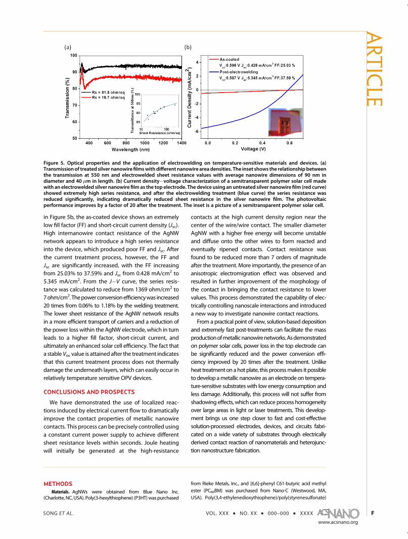
in Figure 5b, the as-coated device shows an extremelylow fill factor (FF) and short-circuit current density (Jsc).High internanowire contact resistance of the AgNWnetwork appears to introduce a high series resistanceinto the device, which produced poor FF and Jsc. Afterthe current treatment process, however, the FF andJsc are significantly increased, with the FF increasingfrom 25.03% to 37.59% and Jsc from 0.428 mA/cm2 to5.345 mA/cm2. From the J�V curve, the series resis-tance was calculated to reduce from 1369 ohm/cm2 to7ohm/cm2.Thepowerconversionefficiencywas increased20 times from 0.06% to 1.18% by the welding treatment.The lower sheet resistance of the AgNW network resultsin a more efficient transport of carriers and a reduction ofthe power loss within the AgNW electrode, which in turnleads to a higher fill factor, short-circuit current, andultimately an enhanced solar cell efficiency. The fact thata stableVoc value is attained after the treatment indicatesthat this current treatment process does not thermallydamage the underneath layers, which can easily occur inrelatively temperature sensitive OPV devices.
CONCLUSIONS AND PROSPECTS
We have demonstrated the use of localized reac-tions induced by electrical current flow to dramaticallyimprove the contact properties of metallic nanowirecontacts. This process can be precisely controlled usinga constant current power supply to achieve differentsheet resistance levels within seconds. Joule heatingwill initially be generated at the high-resistance
contacts at the high current density region near thecenter of the wire/wire contact. The smaller diameterAgNW with a higher free energy will become unstableand diffuse onto the other wires to form reacted andeventually ripened contacts. Contact resistance wasfound to be reduced more than 7 orders of magnitudeafter the treatment. More importantly, the presence of ananisotropic electromigration effect was observed andresulted in further improvement of the morphology ofthe contact in bringing the contact resistance to lowervalues. This process demonstrated the capability of elec-trically controlling nanoscale interactions and introduceda new way to investigate nanowire contact reactions.From a practical point of view, solution-based deposition
and extremely fast post-treatments can facilitate the massproductionofmetallicnanowirenetworks.Asdemonstratedon polymer solar cells, power loss in the top electrode canbe significantly reduced and the power conversion effi-ciency improved by 20 times after the treatment. Unlikeheat treatmentonahot plate, this processmakes it possibleto develop ametallic nanowire as an electrode on tempera-ture-sensitive substrates with low energy consumption andless damage. Additionally, this process will not suffer fromshadowing effects, which can reduce process homogeneityover large areas in light or laser treatments. This develop-ment brings us one step closer to fast and cost-effectivesolution-processed electrodes, devices, and circuits fabri-cated on a wide variety of substrates through electricallyderived contact reaction of nanomaterials and heterojunc-tion nanostructure fabrication.
METHODSMaterials. AgNWs were obtained from Blue Nano Inc.
(Charlotte,NC,USA). Poly(3-hexylthiophene) (P3HT)waspurchased
from Rieke Metals, Inc., and [6,6]-phenyl C61-butyric acid methylester (PC60BM) was purchased from Nano-C (Westwood, MA,USA). Poly(3,4-ethylenedioxythiophene)/poly(styrenesulfonate)
Figure 5. Optical properties and the application of electrowelding on temperature-sensitive materials and devices. (a)Transmissionof treated silver nanowirefilmswithdifferent nanowire areadensities. The inset shows the relationship betweenthe transmission at 550 nm and electrowelded sheet resistance values with average nanowire dimensions of 90 nm indiameter and 40 μm in length. (b) Current density�voltage characterization of a semitransparent polymer solar cell madewith an electrowelded silver nanowirefilm as the top electrode. The device using an untreated silver nanowirefilm (red curve)showed extremely high series resistance, and after the electrowelding treatment (blue curve) the series resistance wasreduced significantly, indicating dramatically reduced sheet resistance in the silver nanowire film. The photovoltaicperformance improves by a factor of 20 after the treatment. The inset is a picture of a semitransparent polymer solar cell.
ARTIC
LE

SONG ET AL . VOL. XXX ’ NO. XX ’ 000–000 ’ XXXX
www.acsnano.org
G
(PEDOT:PSS, CLEVIOS P VP Al 4083) was purchased fromH. C. Starck (Newton, MA, USA). ZnO nanoparticle solutions wereprepared according to a previous report.35
Characterization of Silver Nanowire Electrodes. SEM images weretaken on a Nova Nano 230 electron microscope, and cross-section SEM images were taken by a FEI Nova 600 NanolabDualbeam SEM/FIB for structural properties of the nanowirecontact. The transmittance spectra were taken using a Hitachiultraviolet�visible spectrophotometer (U-4100). Thermally eva-porated Cr/Au (2 nm/50 nm) through the shadow mask wasused as the metal pads on a glass substrate to define the 0.6 cmin length (L) and 1.2 cm in width (W) channel. The two-pointprobe method was used to estimate the sheet resistance ofthe film defined by Rsh = R(W/L). After the annealing process,the sheet resistance was also tested using a four-point probemethod with a sheet resistivity meter (Guardian Manufacturing,model SRM-232-100, range 0 to 100 ohm/sq) to varify the value.An HP E3631A Triple output direct current power supply with25 V compliance voltage was used to apply current to theAgNW network. The resistance was converted by the voltage,and current recorded in the process and then transferred to thesheet resistance for comparison.
Device Fabrication and Characterization. Different AgNW areadensities as transparent conductors are prepared by mulitpletimes of spin-casting with a AgNW dispersion. AgNWs are dis-persed onto the SiO2 substrate and then spin-coated with methylmethacrylate and poly(methylmethacrylate) as photoresists (PRs).In order to avoid thermal effects to theAgwire contact, PRs arenotbaked after spin-coating. Ag films of 100 nm were patterned bye-beam lithography and then deposited to serve as electrodes.AgNW contact resistance measurements were performed on anAgilent semiconductor parameter analyzer using 0.1 V and con-nected to a 500 ohm resistor. The polymer solar cell device wasfabricated on glass substrates with an ITO transparent electrode.The ZnO nanoparticles were dispersed in ethanol with a concen-trationof 0.1wt%. The ZnOnanoparticle solutionwas spin-coatedonto the substrate and then baked at 120 �C for 5 min underambient conditions as the electron transport layer. P3HT:PC60BMwereblended (1:1, 2wt% in dichlorobenzene) and spin-coated onthe ZnO layer with the slow growth method.36 After annealingat 110 �C for 10 min, the hole transporting material, PEDOT:PSS,was spin-coated on top of the active layer. Finally, AgNWswere spun-cast on top of PEDOT:PSS as the top electrode. J�Vcharacteristics of photovoltaic cells were taken using a Keithley2400 source unit under a simulated AM1.5G spectrum with anOriel 91191 solar simulator. The power was adjusted to 1 sun bycomparing the current to a reference silicon photodiode, usinga KG-5 filter to account for the spectral mismatch.
Simulation. Finite-element method simulations were per-formed using ANSYS Multiphysics software to demonstratethe current crowding at the nanowire contact points. The resultshowing full wires is shown in the Figure SI-1. Contacts withdifferent morphologies were built based on the observation ofSEM images by Solidwork software. The cross-section imageswereused to show the current ditribution in the bulk of the nanowires.
Conflict of Interest: The authors declare no competingfinancial interest.
Acknowledgment. The authors would like to express theirgratitude for the generous financial support of Tokyo ElectronLtd. The authors thank Mr. Noah Bodzin from UCLA for assistantand discussion on SEM-FIB analysis.
Supporting Information Available: Current distribution byfinite-element simulation in the full wires and cross-sectionmode on pristine, reacted, and ripened contact conditions.This material is available free of charge via the Internet athttp://pubs.acs.org.
REFERENCES AND NOTES1. Jing, G. Y.; Duan, H. L.; Sun, X. M.; Zhang, Z. S.; Xu, J.; Li, Y. D.;
Wang, J. X.; Yu, D. P. Surface Effects on Elastic Properties ofSilver Nanowires: Contact Atomic-Force Microscopy. Phys.Rev. B 2006, 73, 235409.
2. Cui, Y.; Lieber, C. M. Functional Nanoscale ElectronicDevices Assembled Using Silicon Nanowire BuildingBlocks. Science 2001, 291, 851–853.
3. Balandin, A. A.; Ghosh, S.; Bao, W.; Calizo, I.; Teweldebrhan,D.; Miao, F.; Lau, C. N. Superior Thermal Conductivity ofSingle-Layer Graphene. Nano Lett. 2008, 8, 902–907.
4. Tao, A.; Sinsermsuksakul, P.; Yang, P. Tunable PlasmonicLattices of Silver Nanocrystals. Nat. Nanotechnol. 2007, 2,435–440.
5. Duan, X.; Huang, Y.; Cui, Y.; Wang, J.; Lieber, C. M. IndiumPhosphide Nanowires as Building Blocks for NanoscaleElectronic and Optoelectronic Devices. Nature 2001, 409,66–69.
6. Landi, B. J.; Ganter, M. J.; Cress, C. D.; DiLeo, R. A.; Raffaelle,R. P. Carbon Nanotubes for Lithium Ion Batteries. EnergyEnviron. Sci. 2009, 2, 638–654.
7. Kong, J.; Franklin, N. R.; Zhou, C.; Chapline, M. G.; Peng, S.;Cho, K.; Dai, H. Nanotube Molecular Wires as ChemicalSensors. Science 2000, 287, 622–625.
8. Wu, Z.; Chen, Z.; Du, X.; Logan, J. M.; Sippel, J.; Nikolou, M.;Kamaras, K.; Reynolds, J. R.; Tanner, D. B.; Hebard, A. F.; et al.Transparent, Conductive Carbon Nanotube Films. Science2004, 305, 1273–1276.
9. Hu, L.; Hecht, D. S.; Gruner, G. Percolation in Transparentand Conducting Carbon Nanotube Networks. Nano Lett.2004, 4, 2513–2517.
10. Khrapach, I.; Withers, F.; Bointon, T. H.; Polyushkin, D. K.;Barnes, W. L.; Russo, S.; Cracium, M. F. Novel HighlyConductive and Transparent Graphene-Based Conductors.Adv. Mater. 2012, 24, 2844–2849.
11. Bae, S.; Kim, H.; Lee, Y.; Xu, X.; Park, J. S.; Zheng, Y.;Balakrishnan, J.; Lei, T.; Kim, H. R.; Song, Y.; et al. Roll-to-Roll Production of 30-Inch Graphene Films for TransparentElectrodes. Nat. Nanotechnol. 2010, 5, 574–578.
12. Lee, J. Y.; Connor, S. T.; Cui, Y.; Peumans, P. Solution-Processed Metal Nanowire Mesh Transparent Electrodes.Nano Lett. 2008, 8, 689–692.
13. Chung, C. H.; Song, T. B.; Bob, B.; Duan, H. S.; Yang, Y. SilverNanowire Composite Window Layers for Fully Solution-Deposited Thin-Film Photovoltaic Devices. Adv. Mater.2012, 24, 5499–5504.
14. Rathmell, A. R.; Wiley, B. J. The Synthesis and Coating ofLong, Thin Copper Nanowires toMake Flexible, TransparentConducting Films on Plastic Substrates. Adv. Mater. 2011,23, 4798–4803.
15. Barnes, T. M.; Reese, M. O.; Bergeson, J. D.; Larsen, B. A.;Blackbum, J. L.; Beard, M. C.; Bult, J.; Lagemaat, J. V. D.Comparing the Fundamental Physics and Device Perfor-mance of Transparent, Conductive Nanostructured Net-works with Conventional Transparent Conducting Oxides.Adv. Energy Mater. 2012, 2, 353–360.
16. Hecht, D. S.; Hu, L.; Irvin, G. Emerging Transparent Electro-des Based on Thin Films of Carbon Nanotubes, Graphene,and Metallic Nanostructures. Adv. Mater. 2011, 23, 1482–1513.
17. Gaynor, W.; Lee, J. Y.; Peumans, P. Fully Solution-ProcessedInverted Polymer Solar Cells with Laminated NanowireElectrodes. ACS Nano 2010, 4, 30–34.
18. Tokuno, T.; Nogi, M.; Karakawa, M.; Jiu, J.; Nge, T. T.; Aso, Y.;Suganuma, K. Fabrication of Silver Nanowire TransparentElectrodes at Room Temperature. Nano Res. 2011, 4,1215–1222.
19. Hu, L.; Kim, H. S.; Lee, J. Y.; Peumans, P.; Cui, Y. ScalableCoating and Properties of Transparent, Flexible, SilverNanowire Electrodes. ACS Nano 2010, 4, 2955–2963.
20. Madaria, A. R.; Kumar, A.; Ishikawa, F. N.; Zhou, C. W.Uniform, Highly Conductive, and Patterned TransparentFilms of a Percolating Silver Nanowire Network on Rigidand Flexible Substrates Using a Dry Transfer Technique.Nano Res. 2010, 3, 564–573.
21. Chung, C. H.; Song, T. B.; Bob, B.; Zhu, R.; Yang, Y. Solution-Processed Flexible Transparent Conductors Composedof Silver Nanowire Networks Embedded in Indium TinOxide Nanoparticle Matrices. Nano Res. 2012, 5, 805–814.
ARTIC
LE

SONG ET AL . VOL. XXX ’ NO. XX ’ 000–000 ’ XXXX
www.acsnano.org
H
22. Zhu, R.; Chung, C. H.; Cha, K. C.; Yang,W.; Zheng, Y. B.; Zhou,H.; Song, T. B.; Chen, C. C.; Weiss, P. S.; Li, G.; et al. FusedSilver Nanowires with Metal Oxide Nanoparticles andOrganic Polymers for Highly Transparent Conductors.ACS Nano 2011, 5, 9877–9882.
23. Garnett, E. C.; Cai, W.; Cha, J. J.; Mahmood, F.; Connor, S. T.;Christoforo, M. G.; Cui, Y.; McGehee, M. D.; Brongersma,M. L. Self-Limited Plasmonic Welding of Silver NanowireJunctions. Nat. Mater. 2012, 11, 241–249.
24. Tohmyoh, H.; Fukui, S. Self-Completed Joule Heat Weldingof Ultrathin Pt Wires. Phys. Rev. B 2009, 80, 155403.
25. Jin, C.; Suenaga, K.; Iijima, S. Plumbing Carbon Nanotubes.Nat. Nanotechnol. 2008, 3, 17–21.
26. Tu, K. N. Recent Advances on Electromigration in Very-Large-Scale-Integration of Interconnects. J. Appl. Phys.2003, 94, 5451.
27. Allen, M. L.; Aronniemi, M.; Mattila, T.; Alastalo, A.;Ojanpera, K.; Suhonen, M.; Seppa, H. Electrical Sinteringof Nanoparticle Structures. Nanotechnology 2008, 19,175201.
28. Alastalo, A. T.; Seppa, H.; Leppäniemi, J. H.; Aronniemi, M. J.;Allen, M. L.; Mattila, T. Modeling of Nanoparticle Sinteringunder Electrical Boundary Conditions. J. Phys. D: Appl.Phys. 2010, 43, 485501.
29. Wakuda, D.; Kim, K. S.; Suganuma, K. Room-TemperatureSintering Process of Ag Nanoparticle Paste. IEEE Trans.Compon. Packag. Technol. 2009, 32, 627–632.
30. Iwama, S.; Hayakawa, K. Sintering of Ultrafine MetalPowders, II: Neck Growth Stage of Au, Ag, Al and Cu. Jpn.J. Appl. Phys. 1981, 20, 335–340.
31. Sanders, D. E.; DePristo, A. E. Predicted Diffusion Rateson FCC (001) Metal Surfaces for Adsorbate/SubstrateCombinations of Ni, Cu, Rh, Pd, Ag, Pt, Au. Surf. Sci.1992, 260, 116–128.
32. Bergin, S. M.; Chen, Y .H.; Rathmell, A. R.; Charbonneau, P.;Li, Z. Y.; Wiley, B. J. The Effect of Nanowire Length andDiameter on the Properties of Transparent, ConductingNanowire Films. Nanoscale 2012, 4, 1996–2004.
33. Yu, Z.; Li, L.; Zhang, Q.; Hu, W.; Pei, Q. Silver Nanowire-Polymer Composite Electrodes for Efficient Polymer SolarCells. Adv. Mater. 2011, 23, 4453–4457.
34. Sorel, S.; Lyons, P. E.; De, S.; Dickerson, J. C.; Coleman, J. N.The Dependence of the Optoelectrical Properties of SilverNanowire Networks on Nanowire Length and Diameter.Nanotechnology 2012, 23, 185201.
35. Chou, C. H.; Kwan, W. L.; Hong, Z.; Chen, L. M.; Yang, Y.Metal-Oxide Interconnection Layer for Polymer TandemSolar Cells with an Inverted Architecture. Adv. Mater. 2011,23, 1282–1286.
36. Li, G.; Shrotriya, V.; Huang, J.; Yao, Y.; Moriarty, T.; Emery, K.;Yang, Y. High-Efficiency Solution Processable PolymerPhotovoltaic Cells by Self-Organization of Polymer Blends.Nat. Mater. 2005, 4, 864–868.
ARTIC
LE