Embed Size (px)
Citation preview
1/56
JJIIJI
Back
Close
Nonlinear effects in Silicon Waveguides
Govind P. AgrawalInstitute of OpticsUniversity of RochesterRochester, NY 14627
c©2007 G. P. Agrawal
2/56
JJIIJI
Back
Close
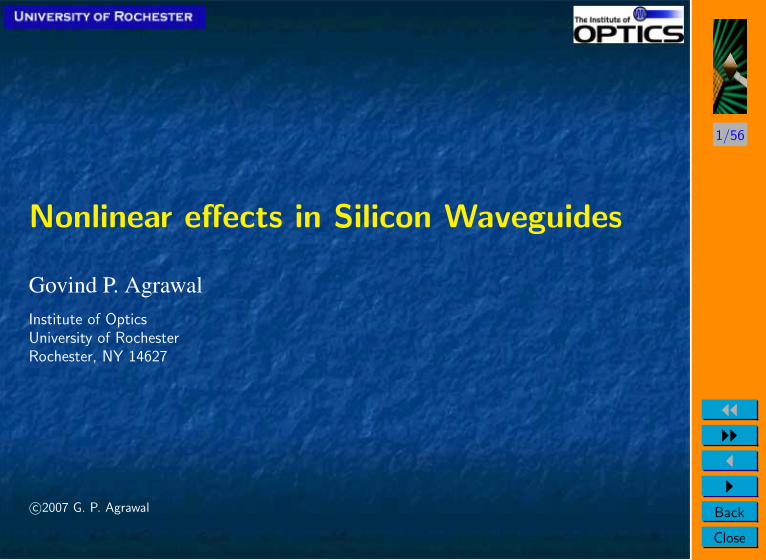
Outline
• Why use silicon for photonics?
• Silicon-on-Insulator (SOI) Waveguides
• Two-Photon Absorption and Free-Carrier Effects
• Self-Phase Modulation and Soliton Formation
• Higher-Order Solitons and Supercontinuum Generation
• Cross-Phase Modulation and Optical Switching
• Four-Wave Mixing and Parametric Amplification
• Raman Amplification and Silicon Raman Lasers
• Concluding Remarks
3/56
JJIIJI
Back
Close
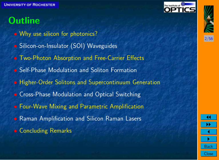
Silicon Photonics
• Silicon dominates microelectronics industry totally.
• Silicon photonics is a new research area trying to capitalize on the
huge investment by the microelectronics industry.
• It has the potential for providing a monolithically integrated
optoelectronic platform on a silicon chip.
Credit: Intel and IBM Websites
4/56
JJIIJI
Back
Close
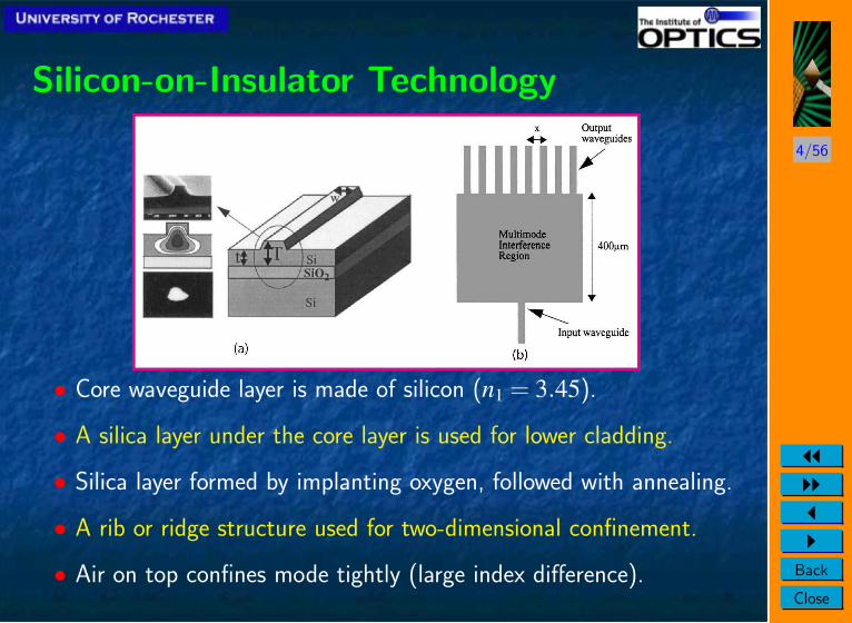
Silicon-on-Insulator Technology
• Core waveguide layer is made of silicon (n1 = 3.45).
• A silica layer under the core layer is used for lower cladding.
• Silica layer formed by implanting oxygen, followed with annealing.
• A rib or ridge structure used for two-dimensional confinement.
• Air on top confines mode tightly (large index difference).
5/56
JJIIJI
Back
Close
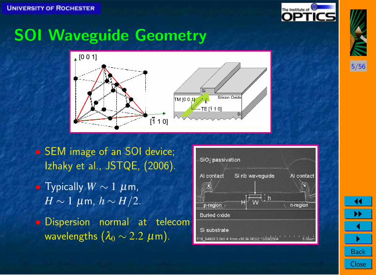
SOI Waveguide Geometry[0 0 1][0 0 1]
[1 1 0][1 1 0]
• SEM image of an SOI device;
Izhaky et al., JSTQE, (2006).
• Typically W ∼ 1 µm,
H ∼ 1 µm, h∼ H/2.
• Dispersion normal at telecom
wavelengths (λ0 ∼ 2.2 µm).
6/56
JJIIJI
Back
Close
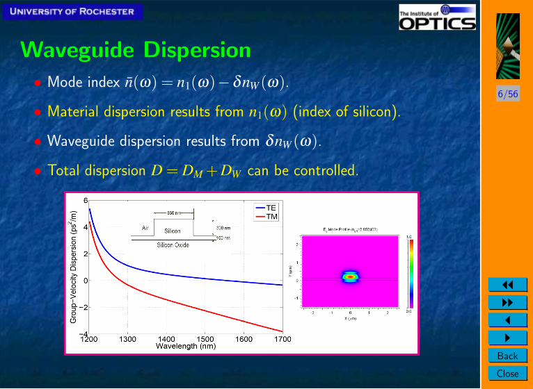
Waveguide Dispersion
• Mode index n(ω) = n1(ω)−δnW(ω).
• Material dispersion results from n1(ω) (index of silicon).
• Waveguide dispersion results from δnW(ω).
• Total dispersion D = DM +DW can be controlled.
7/56
JJIIJI
Back
Close
Major Nonlinear Effects
• Self-Phase Modulation (SPM)
• Cross-Phase Modulation (XPM)
• Four-Wave Mixing (FWM)
• Stimulated Brillouin Scattering (SBS)
• Stimulated Raman Scattering (SRS)
Origin of Nonlinear Effects in Silicon
• Third-order nonlinear susceptibility χ (3).
• Real part leads to SPM, XPM, and FWM.
• Imaginary part leads to two-photon absorption (TPA).
8/56
JJIIJI
Back
Close
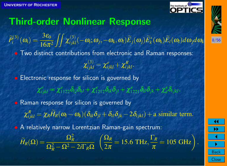
Third-order Nonlinear Response
P(3)i (ωi) =
3ε0
16π2
∫∫χ
(3)i jkl(−ωi;ω j,−ωk,ωl)E j(ω j)E∗k (ωk)El(ωl)dω jdωk
• Two distinct contributions from electronic and Raman responses:
χ(3)i jkl = χ
ei jkl + χ
Ri jkl.
• Electronic response for silicon is governed by
χei jkl = χ
e1122δi jδkl + χ
e1212δikδ jl + χ
e1221δilδ jk + χ
edδi jkl.
• Raman response for silicon is governed by
χRi jkl = χRHR(ωl−ωk)(δikδ jl +δilδ jk−2δi jkl)+ a similar term.
• A relatively narrow Lorentzian Raman-gain spectrum:
HR(Ω)=Ω2
R
Ω2R−Ω2−2iΓRΩ
(ΩR
2π= 15.6 THz,
ΓR
π= 105 GHz
).
9/56
JJIIJI
Back
Close
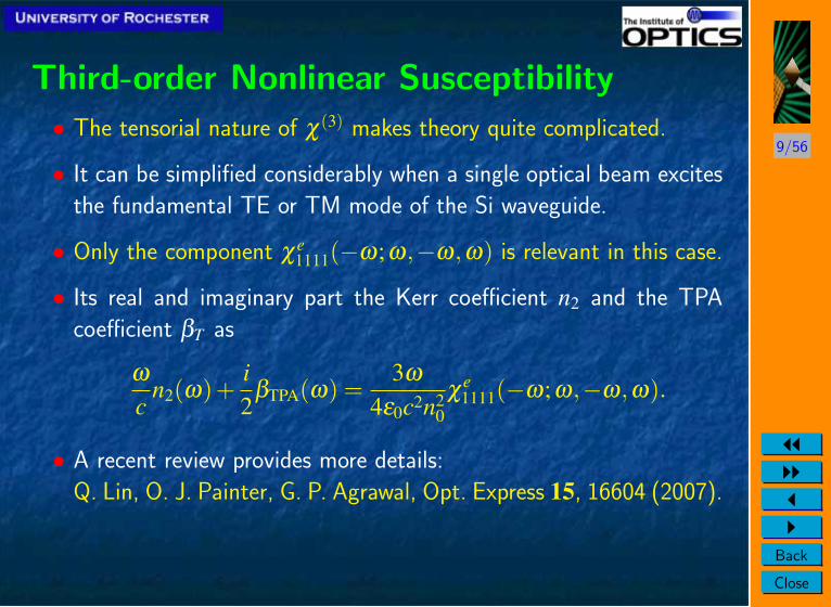
Third-order Nonlinear Susceptibility
• The tensorial nature of χ (3) makes theory quite complicated.
• It can be simplified considerably when a single optical beam excites
the fundamental TE or TM mode of the Si waveguide.
• Only the component χe1111(−ω;ω,−ω,ω) is relevant in this case.
• Its real and imaginary part the Kerr coefficient n2 and the TPA
coefficient βT as
ω
cn2(ω)+
i2
βTPA(ω) =3ω
4ε0c2n20χ
e1111(−ω;ω,−ω,ω).
• A recent review provides more details:
Q. Lin, O. J. Painter, G. P. Agrawal, Opt. Express 15, 16604 (2007).
10/56
JJIIJI
Back
Close
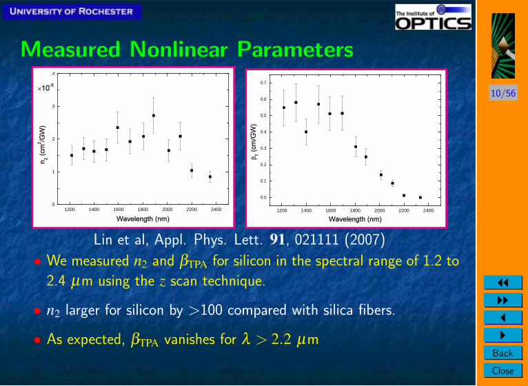
Measured Nonlinear Parameters
1200 1400 1600 1800 2000 2200 24000
1
2
3
4
1200 1400 1600 1800 2000 2200 2400
0.0
0.1
0.2
0.3
0.4
0.5
0.6
0.7
Lin et al, Appl. Phys. Lett. 91, 021111 (2007)
• We measured n2 and βTPA for silicon in the spectral range of 1.2 to
2.4 µm using the z scan technique.
• n2 larger for silicon by >100 compared with silica fibers.
• As expected, βTPA vanishes for λ > 2.2 µm
11/56
JJIIJI
Back
Close
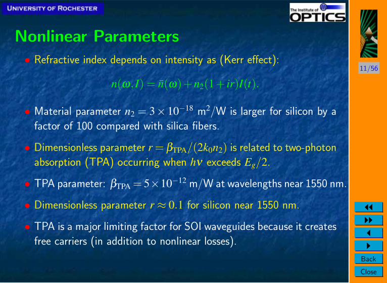
Nonlinear Parameters
• Refractive index depends on intensity as (Kerr effect):
n(ω, I) = n(ω)+n2(1+ ir)I(t).
• Material parameter n2 = 3×10⁻¹⁸ m2/W is larger for silicon by a
factor of 100 compared with silica fibers.
• Dimensionless parameter r = βTPA/(2k0n2) is related to two-photon
absorption (TPA) occurring when hν exceeds Eg/2.
• TPA parameter: βTPA = 5×10⁻¹² m/W at wavelengths near 1550 nm.
• Dimensionless parameter r ≈ 0.1 for silicon near 1550 nm.
• TPA is a major limiting factor for SOI waveguides because it creates
free carriers (in addition to nonlinear losses).
12/56
JJIIJI
Back
Close
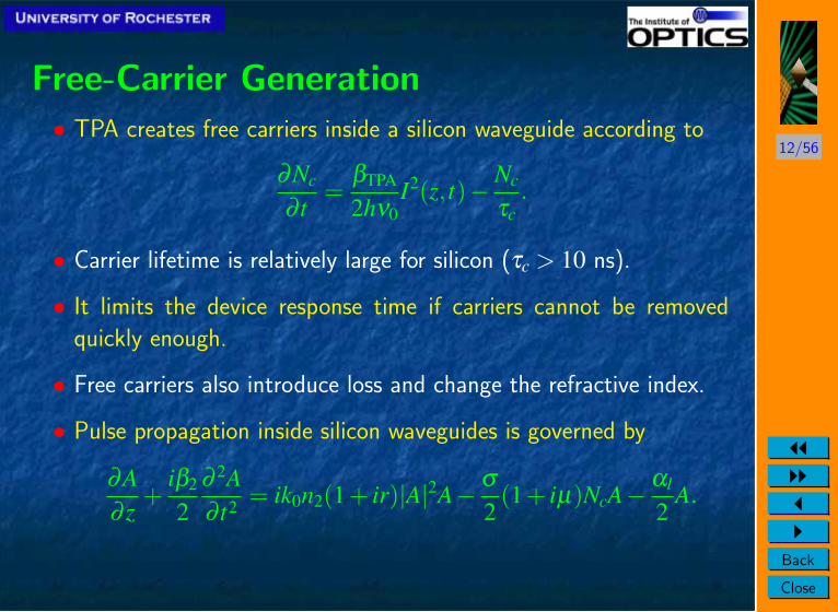
Free-Carrier Generation
• TPA creates free carriers inside a silicon waveguide according to
∂Nc
∂ t=
βTPA
2hν0I2(z, t)− Nc
τc.
• Carrier lifetime is relatively large for silicon (τc > 10 ns).
• It limits the device response time if carriers cannot be removed
quickly enough.
• Free carriers also introduce loss and change the refractive index.
• Pulse propagation inside silicon waveguides is governed by
∂A∂ z
+iβ2
2∂ 2A∂ t2 = ik0n2(1+ ir)|A|2A− σ
2(1+ iµ)NcA−
αl
2A.
13/56
JJIIJI
Back
Close
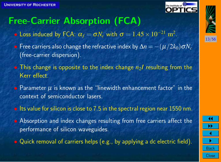
Free-Carrier Absorption (FCA)
• Loss induced by FCA: α f = σNc with σ = 1.45×10⁻²¹ m2.
• Free carriers also change the refractive index by ∆n =−(µ/2k0)σNc
(free-carrier dispersion).
• This change is opposite to the index change n2I resulting from the
Kerr effect.
• Parameter µ is known as the “linewidth enhancement factor” in the
context of semiconductor lasers.
• Its value for silicon is close to 7.5 in the spectral region near 1550 nm.
• Absorption and index changes resulting from free carriers affect the
performance of silicon waveguides.
• Quick removal of carriers helps (e.g., by applying a dc electric field).
14/56
JJIIJI
Back
Close
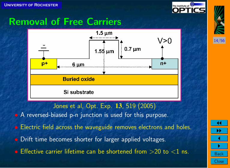
Removal of Free Carriers
Jones et al, Opt. Exp. 13, 519 (2005)
• A reversed-biased p-n junction is used for this purpose.
• Electric field across the waveguide removes electrons and holes.
• Drift time becomes shorter for larger applied voltages.
• Effective carrier lifetime can be shortened from >20 to <1 ns.
15/56
JJIIJI
Back
Close
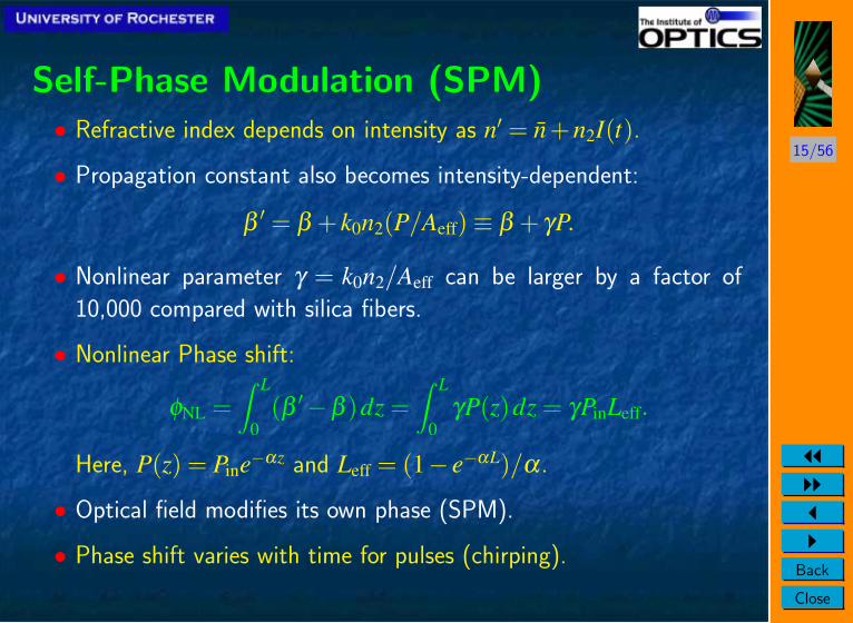
Self-Phase Modulation (SPM)• Refractive index depends on intensity as n′ = n+n2I(t).
• Propagation constant also becomes intensity-dependent:
β′ = β + k0n2(P/Aeff)≡ β + γP.
• Nonlinear parameter γ = k0n2/Aeff can be larger by a factor of
10,000 compared with silica fibers.
• Nonlinear Phase shift:
φNL =∫ L
0(β ′−β )dz =
∫ L
0γP(z)dz = γPinLeff.
Here, P(z) = Pine−αz and Leff = (1− e−αL)/α .
• Optical field modifies its own phase (SPM).
• Phase shift varies with time for pulses (chirping).
16/56
JJIIJI
Back
Close
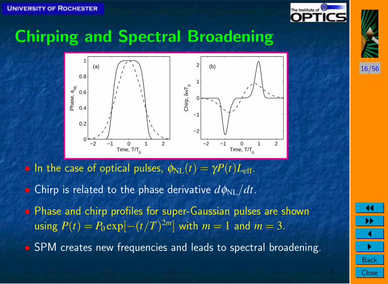
Chirping and Spectral Broadening
−2 −1 0 1 20
0.2
0.4
0.6
0.8
1
Time, T/T0
Pha
se, φ
NL
−2 −1 0 1 2
−2
−1
0
1
2
Time, T/T0
Chi
rp, δ
ωT
0
(a) (b)
• In the case of optical pulses, φNL(t) = γP(t)Leff.
• Chirp is related to the phase derivative dφNL/dt.
• Phase and chirp profiles for super-Gaussian pulses are shown
using P(t) = P0 exp[−(t/T )2m] with m = 1 and m = 3.
• SPM creates new frequencies and leads to spectral broadening.
17/56
JJIIJI
Back
Close
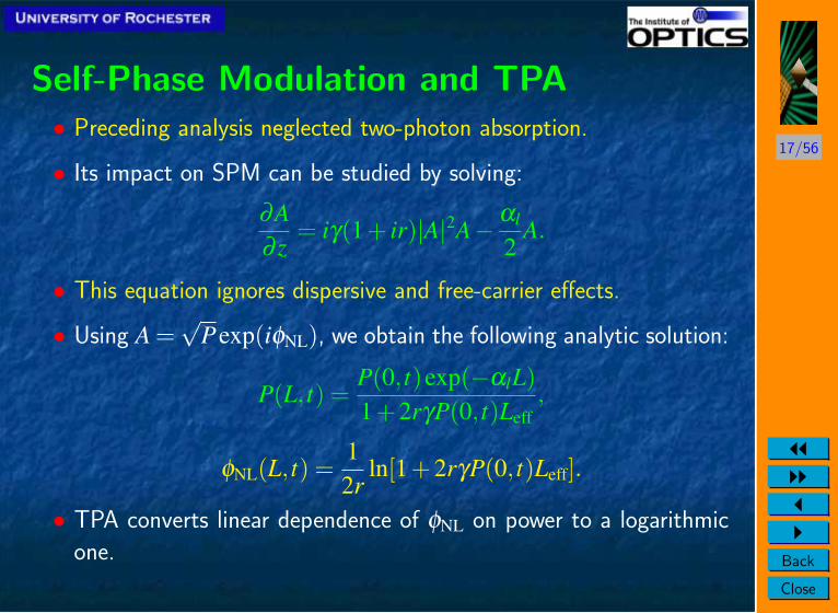
Self-Phase Modulation and TPA• Preceding analysis neglected two-photon absorption.
• Its impact on SPM can be studied by solving:
∂A∂ z
= iγ(1+ ir)|A|2A− αl
2A.
• This equation ignores dispersive and free-carrier effects.
• Using A =√
Pexp(iφNL), we obtain the following analytic solution:
P(L, t) =P(0, t)exp(−αlL)1+2rγP(0, t)Leff
,
φNL(L, t) =12r
ln[1+2rγP(0, t)Leff].
• TPA converts linear dependence of φNL on power to a logarithmic
one.
18/56
JJIIJI
Back
Close
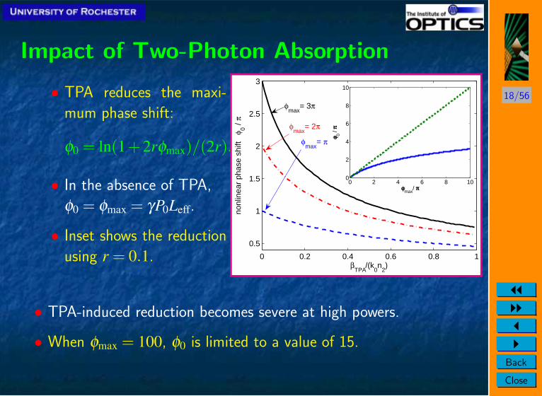
Impact of Two-Photon Absorption
• TPA reduces the maxi-
mum phase shift:
φ0 = ln(1+2rφmax)/(2r).
• In the absence of TPA,
φ0 = φmax = γP0Leff.
• Inset shows the reduction
using r = 0.1. 0 0.2 0.4 0.6 0.8 1
0.5
1
1.5
2
2.5
3
βTPA
/(k0n
2)
nonl
inea
r ph
ase
shift
φ 0 /
π
φmax
= 3π
φmax
= π
φmax
= 2π
0 2 4 6 8 100
2
4
6
8
10
φmax
/ π
φ 0 / π
1
• TPA-induced reduction becomes severe at high powers.
• When φmax = 100, φ0 is limited to a value of 15.
19/56
JJIIJI
Back
Close
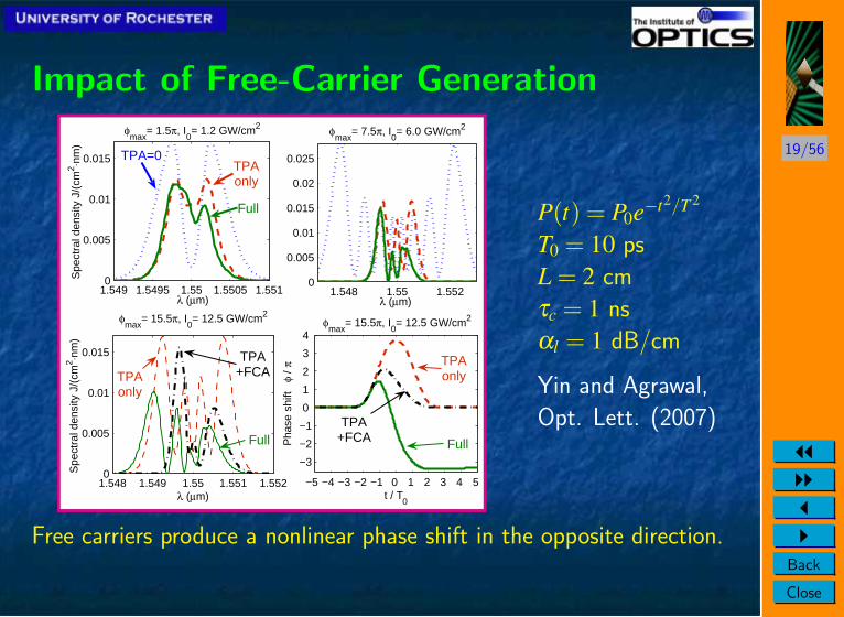
Impact of Free-Carrier Generation
1.549 1.5495 1.55 1.5505 1.5510
0.005
0.01
0.015
λ (µm)
Spe
ctra
l den
sity
J/(
cm2 ⋅n
m)
φmax
= 1.5π, I0= 1.2 GW/cm2
1.548 1.55 1.5520
0.005
0.01
0.015
0.02
0.025
λ (µm)
φmax
= 7.5π, I0= 6.0 GW/cm2
1.548 1.549 1.55 1.551 1.5520
0.005
0.01
0.015
λ (µm)
φmax
= 15.5π, I0= 12.5 GW/cm2
φmax
= 15.5π, I0= 12.5 GW/cm2
Spe
ctra
l den
sity
J/(
cm2 ⋅n
m)
−5 −4 −3 −2 −1 0 1 2 3 4 5
−3
−2
−1
0
1
2
3
4
t / T0
Pha
se s
hift
φ /
π
TPA=0TPAonly
Full
TPA+FCA
Full
TPAonly
TPA+FCA Full
TPAonly
P(t) = P0e−t2/T 2
T0 = 10 ps
L = 2 cm
τc = 1 ns
αl = 1 dB/cm
Yin and Agrawal,
Opt. Lett. (2007)
Free carriers produce a nonlinear phase shift in the opposite direction.
20/56
JJIIJI
Back
Close
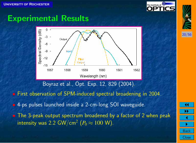
Experimental Results
Boyraz et al., Opt. Exp. 12, 829 (2004).
• First observation of SPM-induced spectral broadening in 2004.
• 4-ps pulses launched inside a 2-cm-long SOI waveguide.
• The 3-peak output spectrum broadened by a factor of 2 when peak
intensity was 2.2 GW/cm2 (P0 ≈ 100 W).
21/56
JJIIJI
Back
Close
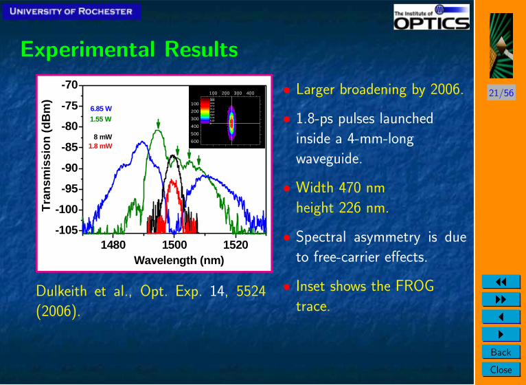
Experimental Results
3. Experimental results and discussion
3.1 Nonlinear-index coefficient n2
Figure 1 shows a series of TE-transmission spectra of the SOI waveguide for different coupled peak powers P at 1500 nm. The two lowest power spectra with P = 1.8 and 8 mW, (corresponding to peak intensities of I ~ 0.003 and 0.014 GW/cm2, respectively) only differ in the transmitted intensity but not in spectral shape and position. The spectral full width at half maximum (FWHM) is identical to pulses measured without sample. Hence, the applied powers of the two low-power spectra belong to the regime where the waveguide is responding optically linear. However, by increasing the peak power to P = 1.55 W (I ≈ 2.6 GW/cm2), the spectral shape of the pulses broadens dramatically; now exhibiting several spectral side wings. The broadening continues for higher powers which can be seen in the spectrum with P = 6.85 W (I ≈ 11.6 GW/cm2).
The measured spectral pulse distortions can be explained by self-phase-modulation, which is known to cause an intensity dependent phase shift of the pulse carrier frequency. Within its own duration, the pulse experiences an intensity- and thus time-dependent refractive index. New frequency components are generated and the initial pulse spectrum broadens in an oscillatory manner while the temporal pulse shape remains unaffected. The degree of SPM-induced spectral broadening depends on the nonlinear refractive index n2 and the waveguide length L. Since the number of spectral oscillations in the transmission spectra is directly correlated with the nonlinear phase shift Φ, we can estimate n2 from the experiment by applying the formula n2 = (Φ · c · Aeff)/(P · Leff · ω) [22]. Leff corresponds to an effective length of the waveguide that is smaller than L because of intrinsic propagation losses.
Assuming a homogeneous and isotropic medium with cubic optical nonlinearity the relation between nonlinear phase shift Φ and number of peaks N in the SPM-broadened spectra is given by Φ ≈ (N - 0.5) · π [22]. However, in the spectra presented in Fig. 1, the peaks are not very pronounced indicating that the applied coupled powers do not cause odd multiples of 0.5 π phase shifts but rather intermediate values. Hence, the visibility of the SPM-induced fringes (self-interference) is reduced making the determination of N difficult. We have therefore applied large error bars allowing the interpretation of either one large or four small peaks (see green arrows in Fig. 1 for 1.55 W). The nonlinear phase shift for the two highest coupled powers then yields Φ = 2 ± 1.5 π and Φ = 3 ± 1.5 π (for 1.55 W and 6.85 W, respectively) resulting in an average nonlinear-index coefficient of about n2 = (5 ± 4) ·10-18
Fig. 1. Transmission spectra of a 4 mm long SOI waveguide as a function of coupled peak power. Linear optical response is observed for low powers (black and red) whereas SPM-induced spectral broadening occurs for high powers (green and blue). Inset: Time- and spectrally resolved FROG trace of input pulses at 1500 nm.
1480 1500 1520-105
-100
-95
-90
-85
-80
-75
-70
1.55 W
8 mW
6.85 W
1.8 mW
Tra
nsm
issi
on
(d
Bm
)
Wavelength (nm)
100 200 300 400
100
200
300
400
500
600
06.2312.518.724.931.237.443.649.953.2
#69591 - $15.00 USD Received 3 April 2006; revised 16 May 2006; accepted 16 May 2006
(C) 2006 OSA 12 June 2006 / Vol. 14, No. 12 / OPTICS EXPRESS 5527
Dulkeith et al., Opt. Exp. 14, 5524
(2006).
• Larger broadening by 2006.
• 1.8-ps pulses launched
inside a 4-mm-long
waveguide.
• Width 470 nm
height 226 nm.
• Spectral asymmetry is due
to free-carrier effects.
• Inset shows the FROG
trace.
22/56
JJIIJI
Back
Close
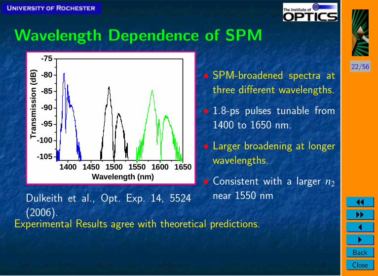
Wavelength Dependence of SPM
3.5 Wavelength dependent SPM
The results in Figs. 1 - 3 demonstrate that nonlinearities such as SPM and TPA-induced FCA strongly perturb the spectral shape of optical pulses at 1500 nm. However, telecommunication bands cover spectral ranges between 1490 nm and 1612 nm (S, C, and L-band). It is therefore of importance to have knowledge about the SPM wavelength dependence.
In order to study this in detail we have measured the spectral broadening as a function of wavelength (1400 – 1650 nm) while keeping coupled power and pulse width constant. Figure 4 compares transmission spectra at 1400 nm and 1650 nm with the spectrum at 1500 nm (same as in Fig. 1). The peak power is set to 6.85 W. At all excitation wavelengths the output spectra are broadened and asymmetric. The significant difference is that SPM-induced broadening becomes more efficient for longer wavelengths. The spectral distance between the short-wavelength SPM oscillation and the originally injected laser wavelength increases from 8 to 16 nm when the OPA is tuned from 1400 to 1650 nm. As will be discussed in the next section, this enhancement for longer wavelengths is probably due to an increase of group index ng and nonlinear refractive index n2.
4. Comparison with theory and discussion
4.1 Model description
To analyze the experimental data we have used a recently developed theoretical model to describe the pulse dynamics in Si photonic wires. It accounts for GVD, parametric and non-parametric nonlinear effects such as SPM, XPM, TPA, or Raman interaction; free carrier-induced effects, such as FCA and free carriers dynamics [31]. In the case studied here, of single-frequency pulse propagation, a simplified version of the model, excluding XPM and Raman terms, is used. The dynamics of pulse propagation in silicon photonic wires is governed by the following system of coupled nonlinear differential equations
22212 1 1
1 20 0
3( )
2 2FC
in FC
nc Pi i i
z t t n n A
ωβ δβ β κ ωβψ ψ ψβ α α ψ ψ ψ ψε
Γ∂ ∂ ∂+ − = − + − −∂ ∂ ∂
(1)
2
4212
0 0
"( ) 6
2c
N NP
t t A
β ψε
Γ∂ Δ Δ= − +∂
(2)
Fig. 4. SPM-induced spectral broadening of optical pulses for the same coupled peak power (6.85 W) injected into the SOI waveguide at 1400, 1500 and 1600 nm. The spectral broadening increases with the wavelength.
1400 1450 1500 1550 1600 1650-105
-100
-95
-90
-85
-80
-75
Tra
nsm
issi
on
(d
B)
Wavelength (nm)
#69591 - $15.00 USD Received 3 April 2006; revised 16 May 2006; accepted 16 May 2006
(C) 2006 OSA 12 June 2006 / Vol. 14, No. 12 / OPTICS EXPRESS 5531
Dulkeith et al., Opt. Exp. 14, 5524
(2006).
• SPM-broadened spectra at
three different wavelengths.
• 1.8-ps pulses tunable from
1400 to 1650 nm.
• Larger broadening at longer
wavelengths.
• Consistent with a larger n2
near 1550 nm
Experimental Results agree with theoretical predictions.
23/56
JJIIJI
Back
Close
Formation of Optical Solitons• SPM-induced phase shift φNL > 1 is easily realized.
• φNL = 1 occurs at z = LNL = 1/(γP0).
• Nonlinear length LNL ∼1 cm at moderate peak powers <10 W.
• Dispersion length (LD = T 20 /|β2) can also be made∼1 cm for pulses
100-fs wide or less.
• Pulses propagate as fundamental solitons (N = 1) when
N2 =LD
LNL=
γP0T 20
|β2= 1.
• Formation of optical solitons possible if waveguide is designed to
provide anomalous dispersion at the operating wavelength.
• Numerical simulations confirm this expectation.
24/56
JJIIJI
Back
Close
Formation of Optical Solitons
500 400 300 200 100 0 100 200 300 400 5000
0.2
0.4
0.6
0.8
1P ulse S hape
time (fs )
No
rma
lize
d P
ow
er
1.51 1.52 1.53 1.54 1.55 1.56 1.57 1.58 1.590
0.2
0.4
0.6
0.8
1P ulse S pectrum
Sp
ect
ral D
en
sity
Input
T P A
Input
P ath averaged
α
T P A
P ath averaged
Wavelength (µm)
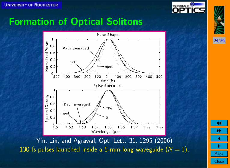
Yin, Lin, and Agrawal, Opt. Lett. 31, 1295 (2006)
130-fs pulses launched inside a 5-mm-long waveguide (N = 1).
25/56
JJIIJI
Back
Close
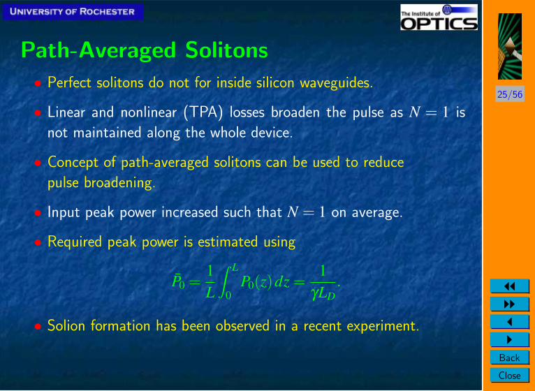
Path-Averaged Solitons
• Perfect solitons do not for inside silicon waveguides.
• Linear and nonlinear (TPA) losses broaden the pulse as N = 1 is
not maintained along the whole device.
• Concept of path-averaged solitons can be used to reduce
pulse broadening.
• Input peak power increased such that N = 1 on average.
• Required peak power is estimated using
P0 =1L
∫ L
0P0(z)dz =
1γLD
.
• Solion formation has been observed in a recent experiment.
26/56
JJIIJI
Back
Close
Observation of Optical Solitons
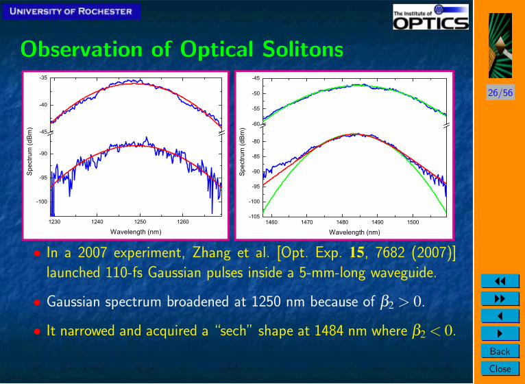
• In a 2007 experiment, Zhang et al. [Opt. Exp. 15, 7682 (2007)]
launched 110-fs Gaussian pulses inside a 5-mm-long waveguide.
• Gaussian spectrum broadened at 1250 nm because of β2 > 0.
• It narrowed and acquired a “sech” shape at 1484 nm where β2 < 0.
27/56
JJIIJI
Back
Close
Numerical Simulations
−8 −6 −4 −2 0 2 4 6 8−40
−35
−30
−25
−20
−15
−10
−5
0
Time τ/T0
Nor
mal
ized
Inte
nsity
(dB
)
1420 1440 1460 1480 1500 1520 1540−40
−35
−30
−25
−20
−15
−10
−5
0
Wavelength (nm)N
orm
aliz
ed S
pect
rum
(dB
)
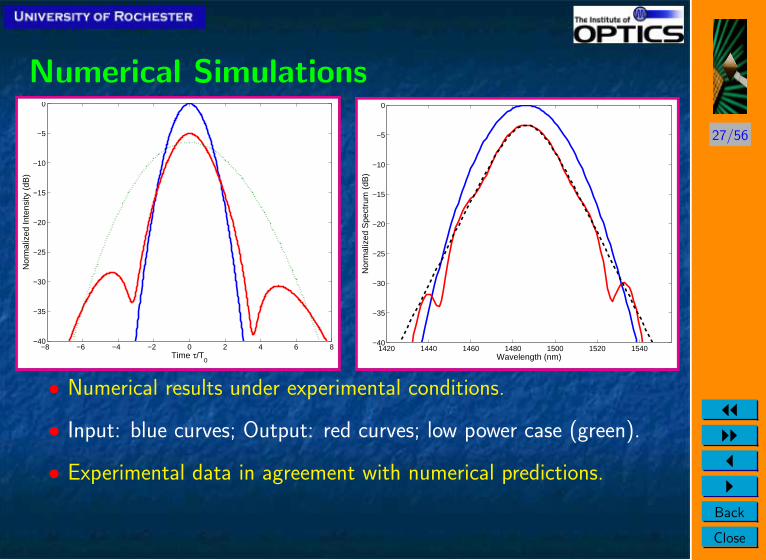
• Numerical results under experimental conditions.
• Input: blue curves; Output: red curves; low power case (green).
• Experimental data in agreement with numerical predictions.
28/56
JJIIJI
Back
Close
Supercontinuum Generation• Ultrashort pulses are affected by a multitude of nonlinear effects,
such as SPM, XPM, FWM, and SRS, together with dispersion.
• All of these nonlinear processes are capable of generating new
frequencies outside the input pulse spectrum.
• For sufficiently intense pulses, the pulse spectrum can become so
broad that it extends over a frequency range exceeding 100 THz.
• Such extreme spectral broadening is referred to as supercontinuum
generation.
• This phenomenon was first observed in solid and gases more than
35 years ago (late 1960s.)
• Since 2000, microstructure fibers have been used for supercontin-
uum generation.
29/56
JJIIJI
Back
Close
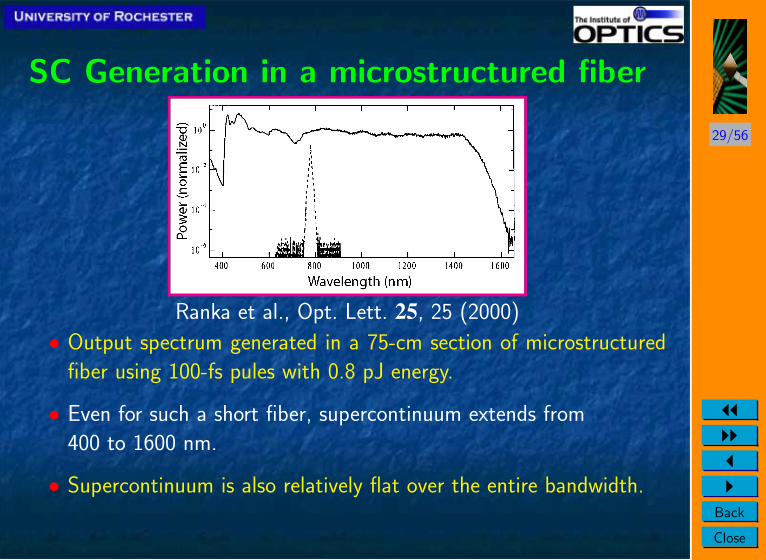
SC Generation in a microstructured fiber
Ranka et al., Opt. Lett. 25, 25 (2000)
• Output spectrum generated in a 75-cm section of microstructured
fiber using 100-fs pules with 0.8 pJ energy.
• Even for such a short fiber, supercontinuum extends from
400 to 1600 nm.
• Supercontinuum is also relatively flat over the entire bandwidth.
30/56
JJIIJI
Back
Close
SC Generation through Soliton Fission
• Input pulses correspond to a higher-order soliton of large order;
typically N = (γP0T 20 /|β2|)1/2 exceeds 5.
• Higher-order effects lead to their fission into much narrower
fundamental solitons: Tk = T0/(2N +1−2k).
• Each of these solitons is affected by intrapulse Raman scattering.
• Spectrum of each soliton is shifted toward longer and longer wave-
lengths with propagation inside the fiber.
• At the same time, each soliton emits nonsolitonic radiation at a
different wavelength on the blue side.
• XPM and FWM generate additional bandwidth and lead to a broad
supercontinuum.
31/56
JJIIJI
Back
Close
SC Generation in Silicon Waveguides• SOI waveguides also support higher-order solitons when
N = (γP0T 20 /|β2|)1/2 exceeds 1.
• Higher-order dispersion leads to their fission into much
shorter fundamental solitons: Tk = T0/(2N +1−2k).
• Spectrum of each soliton shifts toward longer wavelengths by a
smaller amount because of a narrower Raman-gain spectrum of sil-
icon.
• Similar to the case of optical fibers, each soliton is expected to emit
dispersive waves with frequencies on the blue side.
• Numerical simulations confirm the potential of SOI waveguides for
SC generation.
• Spectral broadening over 350 nm is predicted for femtoseond pulses.
32/56
JJIIJI
Back
Close
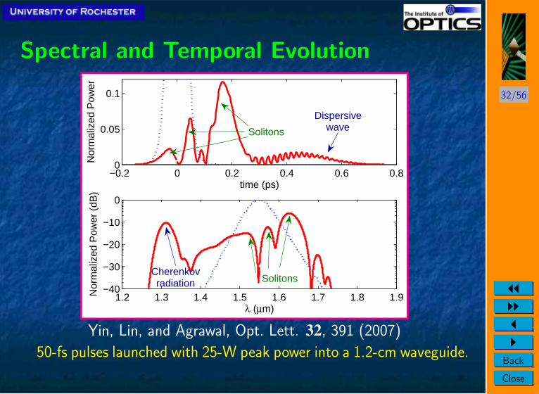
Spectral and Temporal Evolution
−0.2 0 0.2 0.4 0.6 0.80
0.05
0.1
time (ps)
Nor
mal
ized
Pow
er
1.2 1.3 1.4 1.5 1.6 1.7 1.8 1.9
0
−10
−20
−30
−40
λ (µm)
Nor
mal
ized
Pow
er (
dB)
DispersivewaveSolitons
Cherenkovradiation Solitons
Yin, Lin, and Agrawal, Opt. Lett. 32, 391 (2007)
50-fs pulses launched with 25-W peak power into a 1.2-cm waveguide.
33/56
JJIIJI
Back
Close
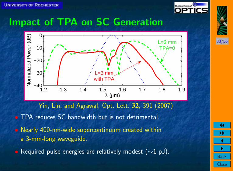
Impact of TPA on SC Generation
1.2 1.3 1.4 1.5 1.6 1.7 1.8 1.9
0
−10
−20
−30
−40
λ (µm)
Nor
mal
ized
Pow
er (
dB)
L=3 mmwith TPA
L=3 mmTPA=0
Yin, Lin, and Agrawal, Opt. Lett. 32, 391 (2007)
• TPA reduces SC bandwidth but is not detrimental.
• Nearly 400-nm-wide supercontinuum created within
a 3-mm-long waveguide.
• Required pulse energies are relatively modest (∼1 pJ).
34/56
JJIIJI
Back
Close
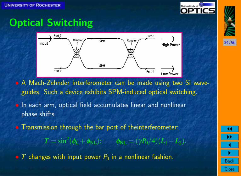
Optical Switching
• A Mach-Zehnder interferometer can be made using two Si wave-
guides. Such a device exhibits SPM-induced optical switching.
• In each arm, optical field accumulates linear and nonlinear
phase shifts.
• Transmission through the bar port of theinterferometer:
T = sin2(φL +φNL); φNL = (γP0/4)(L1−L2).
• T changes with input power P0 in a nonlinear fashion.
35/56
JJIIJI
Back
Close
Cross-Phase Modulation
• Consider two optical fields propagating simultaneously.
• Nonlinear refractive index seen by one wave depends on the
intensity of the other wave as
∆nNL = n2(|A1|2 +b|A2|2).
• Total nonlinear phase shift in a fiber of length L:
φNL = (2πL/λ )n2[I1(t)+bI2(t)].
• An optical beam modifies not only its own phase but also of other
copropagating beams (XPM).
• XPM induces nonlinear coupling among overlapping optical pulses.
36/56
JJIIJI
Back
Close
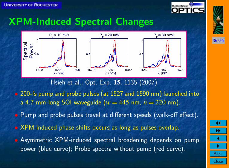
XPM-Induced Spectral Changes
Hsieh et al., Opt. Exp. 15, 1135 (2007)
• 200-fs pump and probe pulses (at 1527 and 1590 nm) launched into
a 4.7-mm-long SOI waveguide (w = 445 nm, h = 220 nm).
• Pump and probe pulses travel at different speeds (walk-off effect).
• XPM-induced phase shifts occurs as long as pulses overlap.
• Asymmetric XPM-induced spectral broadening depends on pump
power (blue curve); Probe spectra without pump (red curve).
37/56
JJIIJI
Back
Close
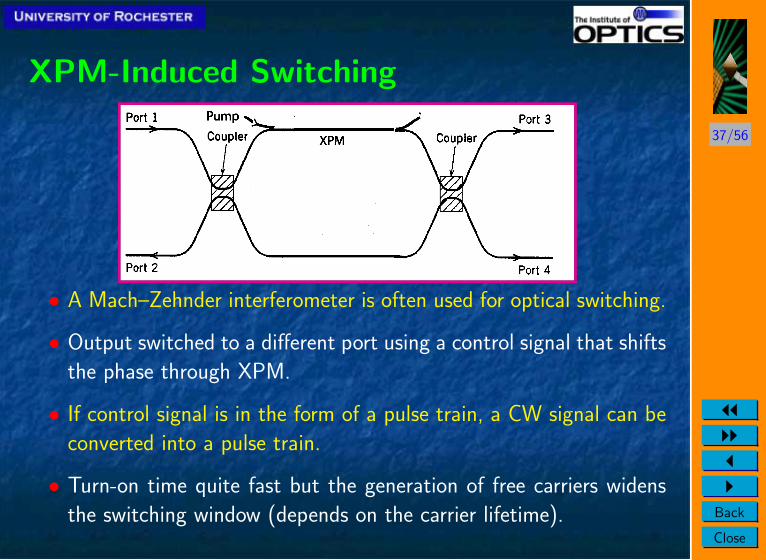
XPM-Induced Switching
• A Mach–Zehnder interferometer is often used for optical switching.
• Output switched to a different port using a control signal that shifts
the phase through XPM.
• If control signal is in the form of a pulse train, a CW signal can be
converted into a pulse train.
• Turn-on time quite fast but the generation of free carriers widens
the switching window (depends on the carrier lifetime).
38/56
JJIIJI
Back
Close
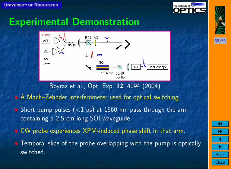
Experimental Demonstration
Boyraz et al., Opt. Exp. 12, 4094 (2004)
• A Mach–Zehnder interferometer used for optical switching.
• Short pump pulses (<1 ps) at 1560 nm pass through the arm
containing a 2.5-cm-long SOI waveguide.
• CW probe experiences XPM-induced phase shift in that arm.
• Temporal slice of the probe overlapping with the pump is optically
switched.
39/56
JJIIJI
Back
Close
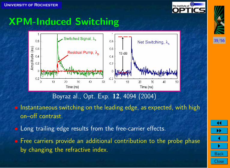
XPM-Induced Switching
Boyraz al., Opt. Exp. 12, 4094 (2004)
• Instantaneous switching on the leading edge, as expected, with high
on–off contrast.
• Long trailing edge results from the free-carrier effects.
• Free carriers provide an additional contribution to the probe phase
by changing the refractive index.
40/56
JJIIJI
Back
Close
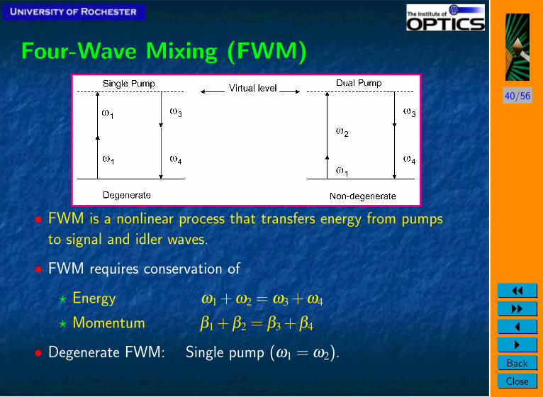
Four-Wave Mixing (FWM)
• FWM is a nonlinear process that transfers energy from pumps
to signal and idler waves.
• FWM requires conservation of
? Energy ω1 +ω2 = ω3 +ω4
? Momentum β1 +β2 = β3 +β4
• Degenerate FWM: Single pump (ω1 = ω2).
41/56
JJIIJI
Back
Close
Parametric Amplifiers• FWM can be used to amplify a weak signal.
• Pump power is transferred to signal through FWM.
• The idler (generated as a byproduct) acts as a copy of the signal at
a new wavelength (useful for wavelength conversion).
• Parametric amplifiers can provide gain at any wavelength using
suitable pumps.
• They are also useful for all-optical signal processing.
• Optical fibers are often used, but the use of SOI waveguides would
result in a much more compact device.
• Impact of two-photon and free-carrier absorption requires further
study.
42/56
JJIIJI
Back
Close
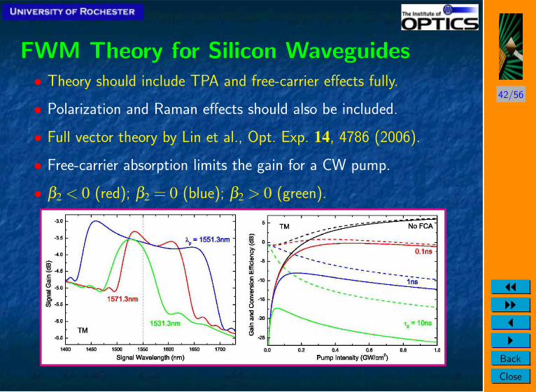
FWM Theory for Silicon Waveguides• Theory should include TPA and free-carrier effects fully.
• Polarization and Raman effects should also be included.
• Full vector theory by Lin et al., Opt. Exp. 14, 4786 (2006).
• Free-carrier absorption limits the gain for a CW pump.
• β2 < 0 (red); β2 = 0 (blue); β2 > 0 (green).
43/56
JJIIJI
Back
Close
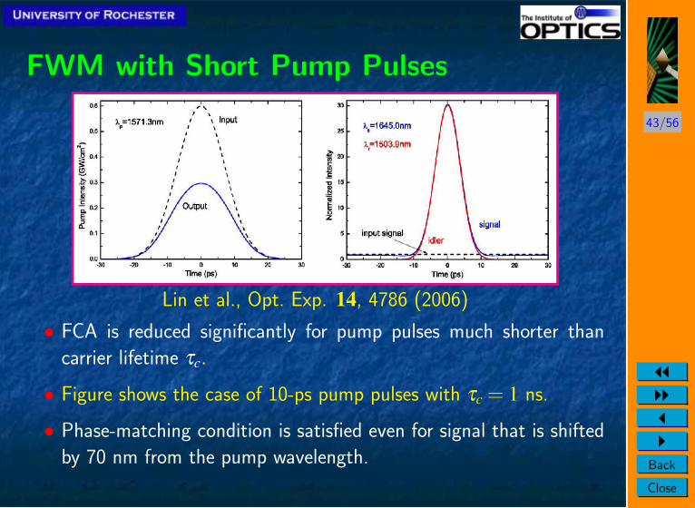
FWM with Short Pump Pulses
Lin et al., Opt. Exp. 14, 4786 (2006)
• FCA is reduced significantly for pump pulses much shorter than
carrier lifetime τc.
• Figure shows the case of 10-ps pump pulses with τc = 1 ns.
• Phase-matching condition is satisfied even for signal that is shifted
by 70 nm from the pump wavelength.
44/56
JJIIJI
Back
Close
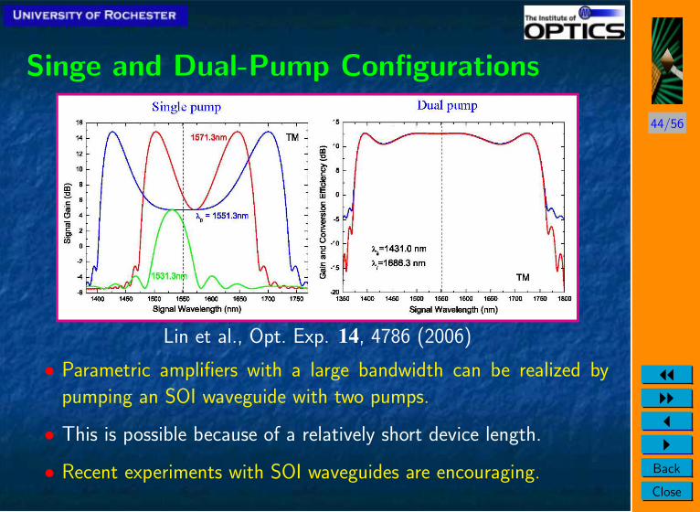
Singe and Dual-Pump Configurations
Lin et al., Opt. Exp. 14, 4786 (2006)
• Parametric amplifiers with a large bandwidth can be realized by
pumping an SOI waveguide with two pumps.
• This is possible because of a relatively short device length.
• Recent experiments with SOI waveguides are encouraging.
45/56
JJIIJI
Back
Close
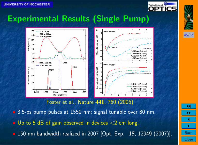
Experimental Results (Single Pump)
Foster et al., Nature 441, 760 (2006)
• 3.5-ps pump pulses at 1550 nm; signal tunable over 80 nm.
• Up to 5 dB of gain observed in devices <2 cm long.
• 150-nm bandwidth realized in 2007 [Opt. Exp. 15, 12949 (2007)].
46/56
JJIIJI
Back
Close
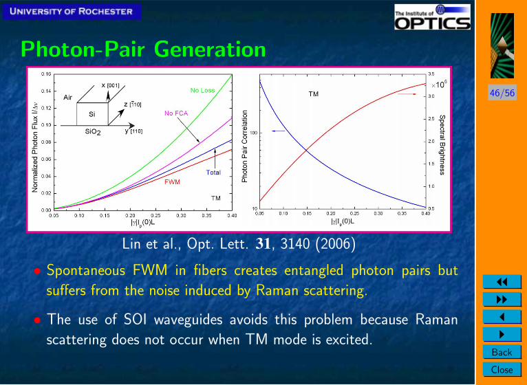
Photon-Pair Generation
Lin et al., Opt. Lett. 31, 3140 (2006)
• Spontaneous FWM in fibers creates entangled photon pairs but
suffers from the noise induced by Raman scattering.
• The use of SOI waveguides avoids this problem because Raman
scattering does not occur when TM mode is excited.
47/56
JJIIJI
Back
Close
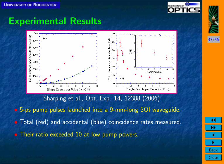
Experimental Results
Sharping et al., Opt. Exp. 14, 12388 (2006)
• 5-ps pump pulses launched into a 9-mm-long SOI waveguide.
• Total (red) and accidental (blue) coincidence rates measured.
• Their ratio exceeded 10 at low pump powers.
48/56
JJIIJI
Back
Close
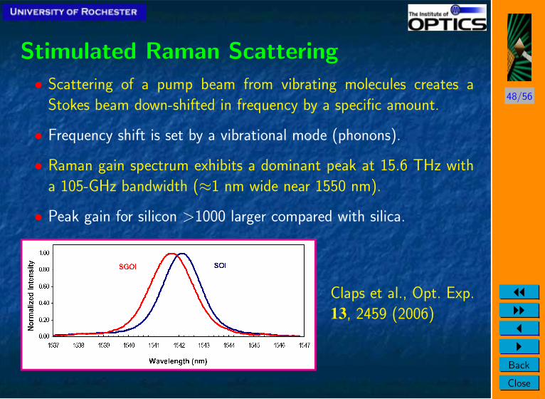
Stimulated Raman Scattering
• Scattering of a pump beam from vibrating molecules creates a
Stokes beam down-shifted in frequency by a specific amount.
• Frequency shift is set by a vibrational mode (phonons).
• Raman gain spectrum exhibits a dominant peak at 15.6 THz with
a 105-GHz bandwidth (≈1 nm wide near 1550 nm).
• Peak gain for silicon >1000 larger compared with silica.
Claps et al., Opt. Exp.
13, 2459 (2006)
49/56
JJIIJI
Back
Close
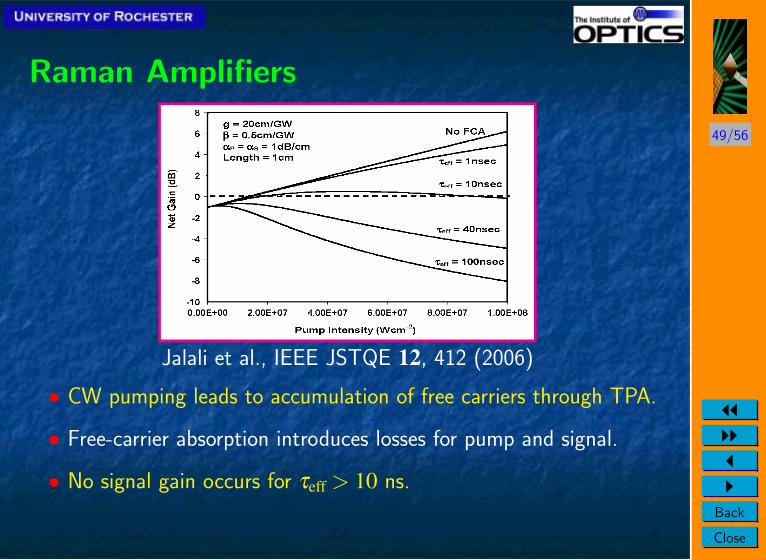
Raman Amplifiers
Jalali et al., IEEE JSTQE 12, 412 (2006)
• CW pumping leads to accumulation of free carriers through TPA.
• Free-carrier absorption introduces losses for pump and signal.
• No signal gain occurs for τeff > 10 ns.
50/56
JJIIJI
Back
Close
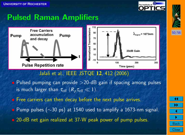
Pulsed Raman Amplifiers
Jalali et al., IEEE JSTQE 12, 412 (2006)
• Pulsed pumping can provide >20-dB gain if spacing among pulses
is much larger than τeff (Rpτeff 1).
• Free carriers can then decay before the next pulse arrives.
• Pump pulses (∼30 ps) at 1540 used to amplify a 1673-nm signal.
• 20-dB net gain realized at 37-W peak power of pump pulses.
51/56
JJIIJI
Back
Close
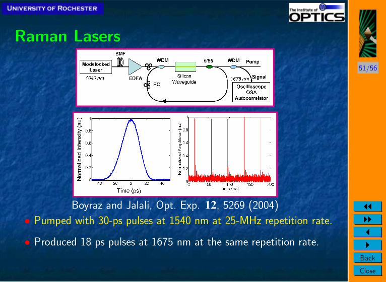
Raman Lasers
Boyraz and Jalali, Opt. Exp. 12, 5269 (2004)
• Pumped with 30-ps pulses at 1540 nm at 25-MHz repetition rate.
• Produced 18 ps pulses at 1675 nm at the same repetition rate.
52/56
JJIIJI
Back
Close
CW Raman Amplifiers
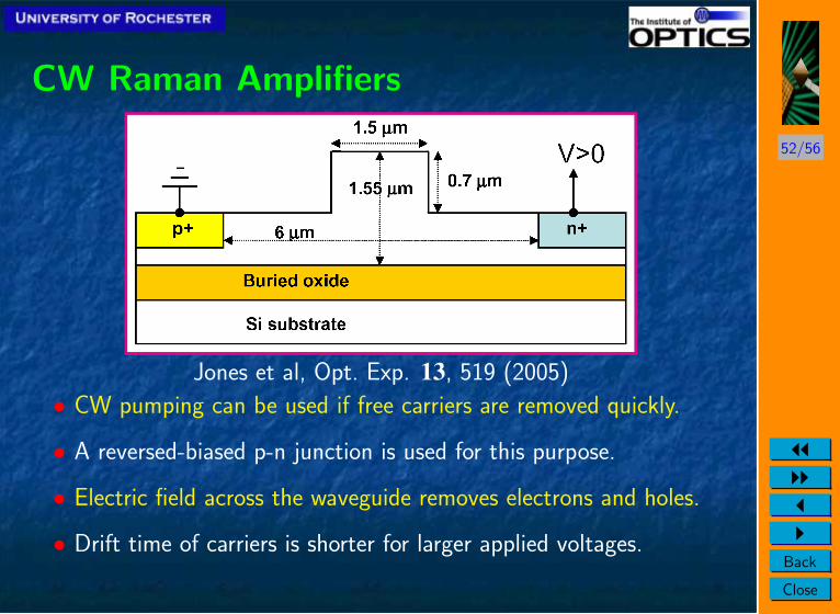
Jones et al, Opt. Exp. 13, 519 (2005)
• CW pumping can be used if free carriers are removed quickly.
• A reversed-biased p-n junction is used for this purpose.
• Electric field across the waveguide removes electrons and holes.
• Drift time of carriers is shorter for larger applied voltages.
53/56
JJIIJI
Back
Close
CW Raman Amplifiers
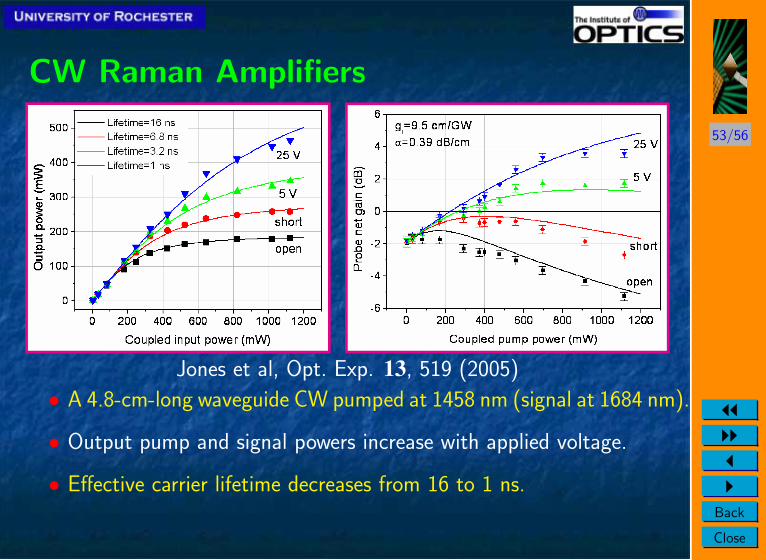
Jones et al, Opt. Exp. 13, 519 (2005)
• A 4.8-cm-long waveguide CW pumped at 1458 nm (signal at 1684 nm).
• Output pump and signal powers increase with applied voltage.
• Effective carrier lifetime decreases from 16 to 1 ns.
54/56
JJIIJI
Back
Close
Theory behind Raman Amplifiers and Lasers
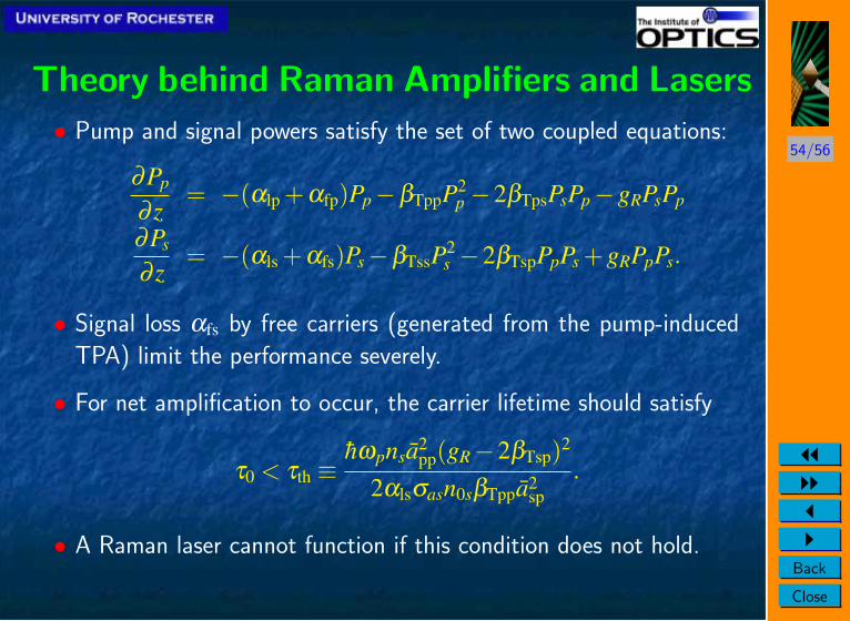
• Pump and signal powers satisfy the set of two coupled equations:
∂Pp
∂ z= −(αlp +αfp)Pp−βTppP2
p −2βTpsPsPp−gRPsPp
∂Ps
∂ z= −(αls +αfs)Ps−βTssP2
s −2βTspPpPs +gRPpPs.
• Signal loss αfs by free carriers (generated from the pump-induced
TPA) limit the performance severely.
• For net amplification to occur, the carrier lifetime should satisfy
τ0 < τth ≡hωpnsa2
pp(gR−2βTsp)2
2αlsσasn0sβTppa2sp
.
• A Raman laser cannot function if this condition does not hold.
55/56
JJIIJI
Back
Close
Concluding Remarks• Nonlinear effects in silicon waveguides can be used to make many
active and passive components.
• SPM is useful for soliton formation and supercontinuum generation.
• SPM and XPM can also be used for optical switching, wavelength
conversion, and all-optical regeneration.
• Four-wave mixing converts silicon waveguides into parametric
amplifiers.
• It can also be used for quantum applications requiring entangled
photon pairs.
• Stimulated Raman scattering converts silicon waveguides into
Raman amplifiers.
56/56
JJIIJI
Back
Close
Further Reading
• L. Pavesi and D. J. Lockwood, Silicon Photonics (Springer, 2004).
• G. T. Reed, Silicon Photonics: State of the Art (Wiley, 2007).
• IEEE J. Sel. Topics Quantum Electron., Special issue on Silicon
Photonics, 12 (2006).
• B. Jalali and S. Fathpour, “Silicon Photonics,” J. Lightwave Tech-
nol. 24, 4600 (2006).
• B. Jalali, “Teaching silicon new tricks,” Nature Photonics 1, 193
(2007).
• Q. Lin, O. J. Painter, G. P. Agrawal, “Nonlinear optical phenomena
in silicon waveguides,” Opt. Express 15, 16604 (2007).