Embed Size (px)
Citation preview

IEEE TRANSACTIONS ON ELECTRON DEVICES 1
Novel Surface Structure and Its Fabrication Processfor MEMS Fingerprint Sensor
Norio Sato, Member, IEEE, Satoshi Shigematsu, Member, IEEE, Hiroki Morimura, Member, IEEE, Masaki Yano,Kazuhisa Kudou, Toshikazu Kamei, and Katsuyuki Machida, Member, IEEE
Abstract—This paper describes a microelectromechanical sys-tems (MEMS) fingerprint sensor that has novel protrusions onthe sensor surface in order to detect clear fingerprint imagesfor various finger surface conditions. A preliminary experimentclarified the importance of contact between soft finger ridges andthe sensor surface in producing fingerprint images. Based on this,novel T-shaped protrusions on the sensor surface are proposed asan interface to mediate the contact. In order to fabricate the over-hung form of the T-shaped structure, photosensitive polyimide anda copper sacrificial layer were used. Using the CMOS-compatibleMEMS fabrication process, the arrayed T-shaped protrusions ofpolyimide are stacked on a CMOS large-scale integrated circuit.The sensor produced clear fingerprint images for various kinds offingers. Measurement of the relationship between applied forceand sensor output showed that the T-shaped protrusions achievedhigh sensitivity regardless of finger elasticity. Reliability testsconfirmed that the sensor with the T-shaped protrusions hassufficient mechanical and electrical strength for wide applications.
Index Terms—CMOS large-scale integrated circuit (LSI),elasticity, fingerprint sensor, microelectromechanical systems(MEMS), sensitivity.
I. INTRODUCTION
PERSONAL identification has become more and more im-portant for higher security in everyday life. One of the ways
to identify people by physical characteristics is by fingerprintidentification. Fingerprint sensors are required to obtain clearimages for every kind of finger surface condition: The sensorshould have a large sensing area corresponding to a fingerprint,and each pixel should be small enough to discriminate fingerridges and valleys. They also should be as small as possible formobile use. Obtained fingerprint images should be clear evenfor dry and wet fingers.
Various types of optical and capacitive fingerprint sensorshave been developed [1]–[6]. Optical fingerprint sensors needillumination components that increase the volume of the sen-sors. Compared to them, capacitive fingerprint sensors have anadvantage in size; they can be small and thin by using large-scaleintegrated circuit (LSI) interconnect technology. However, bothtypes of fingerprint sensors cannot obtain clear images of everytype of finger surface condition including too dry or too moistfingers. The detection principle of optical fingerprint sensors
Manuscript received November 8, 2004. The review of this paper was ar-ranged by Editor K. Najafi.
N. Sato, S. Shigematsu, H. Morimura, and K. Machida are with the NTTMircosystem Integration Laboratories, NTT Corporation, Kanagawa 243-0198,Japan (e-mail: [email protected]).
M. Yano, K. Kudou and T. Kamei are with the NTT Advanced TechnologyCorporation, Kanagawa 243-0198, Japan.
Digital Object Identifier 10.1109/TED.2005.846342
needs complete contact of finger ridges and the sensor surface.In capacitive fingerprint sensors, the moisture of finger ridgesaffects capacitance that is detected by sensing circuits.
In order to overcome the problem, pressure sensors that di-rectly detect the topography of the finger surface were inves-tigated [7], [8]. These sensors have arrays of pixels of about50- m square. Each pixel is a capacitive pressure sensor thathas a movable electrode by finger pressing. This detection prin-ciple will enable the sensor to detect directly the topography ofa finger. However, these sensors in the previous studies did notintegrate a sufficient large number of pixels. Since capacitancebecomes much smaller as the pixel size becomes smaller [9],integration of amplifying circuits below the pixels is necessary.Moreover, the structures of the sensor surface were not designedto accept various kinds of finger and environmental conditions.One of the structures was not sealed and was easily degraded bywater from wet fingers.
We have developed a microelectromechanical systems(MEMS) fingerprint sensor in order to detect the topography ofthe finger surface directly [10]. The sensor has an array of about57 000 pixels 50- m in the area of 11.2 12.8 mm . Eachpixel is a capacitive pressure sensor that has a MEMS cavitystructure stacked on a CMOS LSI. Integrating sensing circuitsjust below the MEMS cavity structures enables a sufficientlylarge number of pixels. The MEMS cavity structure consistsof parallel electrodes and a protrusion with a shape of blockas shown in Fig. 1(a) [10]. When a finger touches the sensorsurface filled with a lot of protrusions, ridges of the fingerdeform the upper electrode via the protrusions and increase thecapacitance between the upper and lower parallel electrodes.The capacitance change is detected by the sensing circuits andconverted into digitized signal levels in the CMOS LSI, andthe detected signals from all the pixels generate one fingerprintimages in gray-scale [11]. Different from the case of capacitivefingerprint sensors [1]–[5], the sensor has parallel electrodesand the finger no longer work as a counter electrode. TheMEMS fingerprint sensor obtained clear fingerprint imagesregardless of whether fingers are dry or wet.
Though our MEMS fingerprint sensor achieved to integratea sufficient number of pixels and to obtain clear images of wetand dry fingers, we found that the sensor sometimes producedunclear fingerprint images. Fingerprint images in Fig. 1(b) and(c) were taken with small and large touching force, respectively.Though the image in Fig. 1(b) is clear, the image in Fig. 1(c) israther unclear. This problem sometimes happens for small num-bers of fingers, which differs from person to person and even forthe same person at different times. We suppose that a situation
0018-9383/$20.00 © 2005 IEEE

2 IEEE TRANSACTIONS ON ELECTRON DEVICES
Fig. 1. (a) Schematic view of a previous MEMS fingerprint sensor; fingerprintimages captured by the MEMS fingerprint sensor with (b) small and (c) largeforce of a person, and (d) schematic view with protrusions buried in a finger.
in which a finger touches the sensor surface may change and theprotrusion may be buried in soft fingers as shown in Fig. 1(d).The protrusions on the surface of the MEMS fingerprint playsome important roles, unlike those encountered with the con-ventional pressure sensors for air or liquid. The relationship be-tween the protrusions and elasticity of fingers has to be clarifiedand the problems regarding unclear fingerprint images shouldbe solved for the MEMS fingerprint sensor.
We have investigated the situation between the finger andthe shape of protrusions. Based on this, we propose a highlysensitive surface structure that enables fingerprint to be detectedat various elasticities and forces. We construct a fabricationprocess of the MEMS structure, which is compatible to CMOSLSIs.
This paper first clarifies the practical situation of contact be-tween a finger and the sensor surface, and proposes the newstructure of protrusion. Next, we explain the fabrication processof the MEMS fingerprint sensor with the new protrusions. Fi-nally, we describe the fabricated sensor chip, reliability tests,and evaluation of the sensitivity.
II. HIGHLY SENSITIVE STRUCTURE
We define sensitivity as a ratio of the change in output of afingerprint image to the change in force when a finger pressesdown on the sensor. If the change in input is small but the changein output is large, then the ratio gives a large value for the sensi-tivity. In order to enhance the sensitivity, the force from a fingershould deform the upper electrode most efficiently to produceas large capacitance change as possible.
The protrusions have a role to propagate force from thefinger to the upper electrode. If there were no protrusions, theridges could not deform the upper electrode, because the upperelectrode is much harder than fingers and is supported by the
Fig. 2. (a) Photograph of sensor surface after fine black particles weresprinkled on areas the finger had touched and (b) schematic cross-sectionalview along line XX’ in (a).
grounded wall. The upper electrode is bent most efficientlywhen the force from finger ridges is concentrated at the center.When the finger ridges only touch the top of the protrusionsas shown in Fig. 1(a), they deform the upper electrode mostefficiently, because the protrusions locate at the center of eachpixel. When the finger ridges touch not only the top of theprotrusions but also the area around them, the force disperseson the area around the protrusions as shown in Fig. 1(d) anddoes not deform the upper electrode efficiently.
To clarify which situation above the practical situation of thecontacts corresponds to, we performed a preliminary experi-ment. We sprinkled fine black particles on the sensor surfaceafter the finger had been lifted off. The particles adhered to thesweat or moisture from the finger on the area that was touched,since sweat and moisture act as an adhesion layer. Fig. 2(a) and(b) shows the sensor surface and schematic cross-sectional viewafter the fine particles were sprinkled. As shown in Fig. 2(a),the black particles made line patterns that corresponded to thefinger ridges and valleys. In the regions corresponding to thefinger valleys, there were no black particles, which shows thatthe protrusions did not touch the finger valleys. In the regionscorresponding to the finger ridges, the black particles adherednot only to the top of 10 m high protrusions but also the areaaround them. Thus, we found that fingers were so soft that theycould actually touch the area around the protrusions and thepractical situation of the contacts was that shown in Fig. 1(d).
The requirement for the protrusions is that they prevent fingerridges from touching the area around them and concentrate theforce at the center of the upper electrode regardless of fingerelasticity. One of the ways to meet the requirement is to lengthenthe height of the protrusions. However, based on a simple esti-mation, the required protrusions are too high to be fabricated asdescribed below. We estimate how deep a protrusion is buriedinto a finger. The MEMS structure with the protrusions andupper electrode can be assumed to be fixed, because Young’smoduli of the protrusions and electrode are much higher (2.5and 78 GPa, respectively) than that of a finger (10–100 kPa[12]–[14]). Assuming a cylindrical protrusion, the buried depth

SATO et al.: NOVEL SURFACE STRUCTURE AND ITS FABRICATION PROCESS 3
Fig. 3. Proposed new structure with T-shaped protrusions.
of a cylindrical protrusion in a finger is analytically expressedas
where is total force, average pressure (area size),is Poisson’s ratio of a finger, is Young’s modulus of a finger,and is a radius of the cylindrical protrusion [12], [15]. Byinserting [5], the area size m ,
, –100 kPa, and m, we obtain the value562.5 to 5625 m as the depth . In order to prevent fingersfrom touching the area around the protrusions, the protrusionsshould be higher than 5625 m in the worst case, which is toothick to be fabricated. Thus, lengthening the protrusions is nota practical solution.
We propose T-shaped protrusions for the sensor to detect fin-gerprints with high sensitivity as shown in Fig. 3. A T-shapedprotrusion has a large area and small spacing between neigh-boring protrusions on top and a small area at the bottom. Theadvantages of this shape are that fingers barely touch the sealinglayer directly and the force is always concentrated at the centerof the upper electrode. The T-shaped protrusions do not requirevery thick film and can be fabricated in the MEMS fabricationprocess.
III. FABRICATION PROCESS
We propose a fabrication process of the MEMS fingerprintsensor with the T-shaped protrusions. The T-shaped protrusionshave overhung parts with spacing from the sealing layer. We de-vised a sacrificial layer etching process to form the shape thatwas succeeded to our previous CMOS-compatible MEMS fab-rication process [10]. Since the spacing should be 3- m andthe protrusions were made of polyimide, we chose copper forforming a thick sacrificial layer and etching copper selectivelyleaving a sealing layer and protrusions of polyimide.
First, the sensing circuits are fabricated in the 0.5- m CMOSLSI and three-metal interconnection process [Fig. 4(a)]. Next,the lower electrodes 1- m thick and the ground wall 2- m thickare gold-electroplated, and the sacrificial layer of photosensitivepolyimide is spin-coated to fill the space between the groundedwall. The top of the grounded wall is exposed by photolithog-raphy. Then, the upper electrode 1- m thick is gold-electro-plated with etch-holes [Fig. 4(b)]. The upper electrode con-tacted with the exposed grounded wall. After that, the sacrifi-cial layer is dry-etched through the etch-holes to make cavities,
Fig. 4. Fabrication process. (a) Sensing circuit fabrication (CMOS process).(b) Au electroplating of electrodes. (c) Sealing of cavity with STP technique.(d) Cu electroplating of sacrificial layer. (e) Patterning of polyimide.(f) Sacrificial layer etching.
and the etch-holes are sealed by the spin-coating film transferand hot-pressing (STP) technique [Fig. 4(c)]. STP can seal ver-tical etch-holes without any sealing material flowing into thecavities [16]–[19]. Fig. 4(d)–(f) explains the proposed processto fabricate the T-shaped protrusions. Seed layers for electro-plating are deposited by evaporating Cu-Ti on the sealing layerof polyimide. The seed layers are each 0.1 m thick. After resistpatterning, we electroplate copper to form a sacrificial layer 3
m thick on the sealing layer. Then, the seed layers are etched[Fig. 4(d)]. After that, photosensitive polyimide 10- m thickis spin-coated and patterned above the grounded wall in a lat-tice pattern [Fig. 4(e)]. Finally, the sacrificial copper layer iswet-etched [Fig. 4(f)].
According to the structural simulation, the edge parts of theT-shaped protrusion floating from the sealing layer with spacingcan be bent when the force is applied equally on the top area.Too large a deformation leads the edge parts to touch the sealinglayer. The key parameters are the thickness of edge parts of theT-shaped protrusions and the distance between the bottom of theedge parts and sealing layer. In order to prevent the contact, we

4 IEEE TRANSACTIONS ON ELECTRON DEVICES
Fig. 5. (a) Fabricated chip photograph. (b) SEM image of T-shapedprotrusions. (c) Magnified image of FIB cross section of a pixel.
TABLE ICHIP SPECIFICATIONS
obtained the value of the thickness of 10 m and distance of 3m for the maximum pressure of 1 MPa based on the simulation.
We used the values in the fabrication process described above.
IV. RESULTS AND DISCUSSION
A. Fabricated MEMS Fingerprint Sensor
We fabricated a MEMS fingerprint sensor chip with theT-shaped protrusions as shown in Fig. 5. The photograph of thechip is shown in Fig. 5(a). The scanning electron microscope(SEM) photograph in Fig. 5(b) shows that the sensor surfaceis filled with the T-shaped protrusions. A magnified image ofa pixel cross section obtained by a focused ion beam (FIB)is shown in Fig. 5(c). The T-shaped protrusions are properlyfabricated on the cavities stacked on the CMOS LSI. The chipspecifications are summarized in Table I. The pixel array has
Fig. 6. Fingerprint images obtained with sensor with T-shaped protrusionswhen force was (a) small; (b) medium; and (c) large.
Fig. 7. Schematic view of evaluation apparatus.
50- m square. The sensing circuitsoutput 8 bit data in gray scale.
The fabricated MEMS fingerprint sensor obtained clear fin-gerprint images of a lot of fingers. It captured clear fingerprintimages when force was small, medium, and large as shown inFig. 6(a), (b) and (c), respectively for the same finger as that inFig. 1(b) and (c).
B. Evaluation of Sensitivity
We evaluated the sensitivity of the sensor by measuring the re-lationship between the output and force using the experimentalapparatus as shown in Fig. 7. The sensor surface is pressed withtest materials, and the output values in gray scale are measuredas the force is increased. We used the sensors with the previousand T-shaped protrusions on the surface as shown in Fig. 1(a)and Fig. 3, respectively. The test materials are a block of foamrubber and a 50- m-thick film. The rubber with and without thefilm corresponds to hard and soft fingers, respectively.
The relationship between output and force is obtained asshown in Fig. 8. For the previous protrusions, it producessmaller output without the film, compared to the output withthe film as shown in Fig. 8(a). The sensitivity is defined as themaximum slope of the line. This graph shows that the sensi-tivity depends on the softness of the material. Fig. 8(b) showsthe results for the T-shaped protrusions. The sensor with theT-shaped protrusions produces large output regardless of thesoftness of the material. Therefore, the T-shaped protrusionsenable various finger elasticities and forces to be detected withhigh sensitivity.
C. Reliability Tests
Since fingerprint sensors are touched by fingers directly, theyshould withstand force and electrostatic discharge (ESD) froma finger, adding to environmental changes required for conven-tional LSIs. The previous investigation on the capacitive-typefingerprint sensor with the underlying CMOS LSI showed thatthe sensor structure and LSI can endure the mechanical, elec-trical, and environmental influences due to touching by fingers[5]. In this section, we describe the mechanical and electricalstrength when the sensor has the MEMS cavity structures.
SATO et al.: NOVEL SURFACE STRUCTURE AND ITS FABRICATION PROCESS 5
Fig. 8. Relationships between force and output for (a) previous and(b) T-shaped protrusions.
Fig. 9. Captured fingerprint image (a) before and (b) after tapping test.
Mechanical strength was evaluated by tapping and rubbingtests. The force loaded on a sensor by a finger in practicaluse consists of vertical and lateral components. We tappedand rubbed the sensor surface with a piece of rubber in orderto evaluate the mechanical strength against vertical force andlateral contact force, respectively. The loaded pressure of 1MPa in the tests was high enough, since the upper limit of thefinger pressure in practical use was measured to be 0.6 MPa[5]. Fig. 9(a) shows the captured fingerprint image before thetapping test. Then, the sensor surface was tapped 100 000 times.The fingerprint image after tapping is shown in Fig. 9(b). Inthe rubbing tests, we rubbed the sensor surface from the top tothe bottom in the images. Fig. 10(a) and (b) shows the imagesbefore and after the rubbing tests. Fig. 10(c) is a magnifiedphotograph of the sensor surface after the test taken by a opticalmicroscope. These images did not change before and after thetests, which shows that the sensor was not damaged by force.The MEMS structure consists of the protrusions, sealing layerand the cavities with the electrodes. We designed the cavity
Fig. 10. Captured fingerprint image (a) before and (b) after rubbing test and,(c) magnified photograph of sensor surface after rubbing test.
Fig. 11. Captured fingerprint image (a) before and (b) after ESD test.
by using structural analysis so as to withstand the pressureof 1 MPa [10]. The adhesion strength between each layerwas high enough to undergo the fabrication and packagingprocesses. These facts result in the mechanical strength of thesensor. Therefore, we confirmed that the sensor has sufficientmechanical strength to withstand finger pressure.
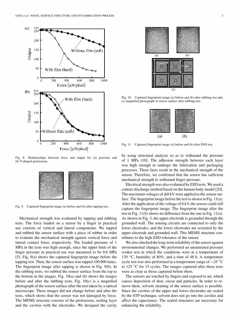
Electrical strength was also evaluated by ESD tests. We used acontact discharge method based on the human body model [20].The maximum voltages of 8 kV were applied to the sensor sur-face. The fingerprint image before the test is shown in Fig. 11(a).After the application of the voltage of 8 kV, the sensor could stillcapture the fingerprint image. The fingerprint image after thetest in Fig. 11(b) shows no difference from the one in Fig. 11(a).As shown in Fig. 3, the upper electrode is grounded through thegrounded wall. The sensing circuits are connected to only thelower electrodes, and the lower electrodes are screened by theupper electrode and grounded wall. This MEMS structure con-tributes to the high ESD tolerance of the sensor.
We also checked the long-term reliability of the sensor againstenvironmental changes. We performed an unsaturated pressurecooker test in which the conditions were at a temperature of130 C, humidity of 80%, and a time of 48 h. A temperaturecycle test was also performed in a temperature range of 25 Cto 125 C for 15 cycles. The images captured after these testswere as clear as those captured before them.
The sensors are touched by fingers and exposed to air, whichcauses deposition of dust, sweat and particles. In order to re-move them, solvent cleaning of the sensor surface is possible.Since the cavities of the upper and lower electrodes are sealedby the STP technique, solvent does not go into the cavities andaffect the capacitance. The sealed structures are necessary forenhancing the reliability.

6 IEEE TRANSACTIONS ON ELECTRON DEVICES
These results show that the sensor has the mechanical andelectrical reliability for long-term use. Therefore, the sensorwith the T-shaped protrusions has high sensitivity even for softfingers, and sufficient reliability as a fingerprint sensor.
V. SUMMARY
We clarified the importance of the relationship betweenelasticity of finger and shape of the protrusion on a surfaceof a MEMS fingerprint sensor with an experiment. Based onthe result, we proposed T-shaped protrusions and devised itsfabrication process by selectively etching a sacrificial layer ofcopper surrounded by polyimide. A fabricated MEMS finger-print sensor has a MEMS cavity structures with the T-shapedprotrusions stacked on a CMOS LSI. The sensor producedclear fingerprint images for various kinds of fingers. Sensitivitymeasurements confirmed that the sensor produces large outputregardless of the elasticity and the sensitivity is enhanced bythe T-shaped protrusions. It is also shown that the sensor hadsufficient mechanical and electrical strength with long-termreliability.
ACKNOWLEDGMENT
The authors would like to thank H. Kyuragi, Y. Kado,T. Ogura, and Y. Okazaki for their helpful support and encour-agement. They also would like to thank Y. Tanabe, S. Yagi,Y. Komine, T. Shimamura, T. Kumazaki, A. Kusayama andN. Sato for their helpful discussions and for the fabrication.
REFERENCES
[1] N. D. Young, G. Harkin, R. M. Bunn, D. J. McCulloch, R. W. Wilks,and A. G. Knapp, “Novel fingerprint scanning arrays using polysiliconTFT’s on glass and polymer substrates,” IEEE Electron Device Lett., vol.18, no. 1, pp. 19–20, Jan. 1997.
[2] M. Tartagni and R. Guerrieri, “A fingerprint sensor based on the feed-back capacitive sensing scheme,” IEEE J. Solid-State Circuits, vol. 33,no. 1, pp. 133–142, Jan. 1998.
[3] D. Inglis, L. Manchanda, R. Comizzoli, A. Dickinson, E. Martin, S.Mendis, P. Silverman, G. Weber, B. Ackland, and L. O’Gorman, “A ro-bust, 1.8 V 250 �W direct-contact 500 dpi fingerprint sensor,” in Proc.ISSCC, Feb. 1998, pp. 284–285.
[4] S. Shigematsu, H. Morimura, Y. Tanabe, T. Adachi, and K. Machida, “Asingle-chip fingerprint sensor and identifier,” IEEE J. Solid-State Cir-cuits, vol. 34, no. 12, pp. 1852–1859, Dec. 1999.
[5] K. Machida, S. Shigematsu, H. Morimura, Y. Tanabe, N. Sato, N.Shimoyama, T. Kumazaki, K. Kudou, M. Yano, and H. Kyuragi, “Anovel semiconductor capacitive sensor for a single-chip fingerprintsensor/identifier LSI,” IEEE Trans. Electron Devices, vol. 48, no. 10,pp. 2273–2278, Oct. 2001.
[6] J. Lan, A. Cole, J. VanZandt, A. Dickinson, F. van de Ven, N. Bird, A.Badano, and J. Kanicki, “Fingerprint imager based on a-Si:H active-ma-trix photo-diode arrays,” in IEDM Tech. Dig., Dec. 2000, pp. 419–422.
[7] R. J. DeSouza and K. D. Wise, “A very high density bulk microma-chined capacitive tactile imager,” in Proc. Transducers, Jun. 1997, pp.1473–1476.
[8] P. Rey, P. Charvet, M. T. Delaye, and S. Abou Hassan, “A high densitycapacitive pressure sensor array for fingerprint sensor application,” inProc. Transducers, Jun. 1997, pp. 1453–1456.
[9] H.-L. Chau and K. D. Wise, “Scaling limits in batch-fabricated siliconpressure sensors,” IEEE Trans. Electron Devices, vol. 34, no. 4, pp.850–858, Apr. 1987.
[10] N. Sato, K. Machida, H. Morimura, S. Shigematsu, K. Kudou, M. Yano,and H. Kyuragi, “MEMS fingerprint sensor immune to various fingersurface conditions,” IEEE Trans. Electron Devices, vol. 50, no. 4, pp.1109–1116, Apr. 2003.
[11] H. Morimura, S. Shigematsu, and K. Machida, “A novel sensor cell ar-chitecture and sensing circuit scheme for capacitive fingerprint sensors,”IEEE J. Solid-State Circuits, vol. 35, no. 5, pp. 724–731, May 2000.
[12] Society of Biomechanisms Japan Ed., Biomechanism 3 (inJapanese). Tokyo, Japan: Univ. of Tokyo Press, 1975, pp. 27–45.
[13] S. Omata, Y. Murayama, and C. E. Constantinou, “Real time robotictactile sensor system for the determination of the physical properties ofbiomaterials,” Sens. Actuators A, Phys., vol. 112, pp. 278–285, 2004.
[14] Y. Murayama and S. Omata, “Fabrication of micro tactile sensor for themeasurement of micro-scale local elasticity,” Sens. Actuators A, Phys.,vol. 109, pp. 202–207, 2004.
[15] I. S. Sokolnikoff, Mathematical Theory of Elasticity, 2nd ed. NewYork: McGraw-Hill Book Company, 1956.
[16] K. Machida, H. Kyuragi, H. Akiya, K. Imai, A. Tounai, and A.Nakashima, “Novel global planarization technology for interlayerdielectrics using spin on glass film transfer and hot pressing,” J. Vac.Sci. Technol., vol. B 16, pp. 1093–1097, 1998.
[17] N. Sato, K. Machida, M. Yano, K. Kudou, and H. Kyuragi, “Advancedspin coating film transfer and hot-pressing process for global planariza-tion with dielectric-material-viscosity control,” Jpn. J. Appl. Phys., vol.41, pp. 2367–2373, 2002.
[18] N. Sato, H. Ishii, S. Shigematsu, H. Morimura, T. Kamei, K. Kudou, M.Yano, K. Machida, and H. Kyuragi, “A sealing technique for stackingMEMS on LSI using spin-coating film transfer and hot pressing,” Jpn.J. Appl. Phys., vol. 42, pp. 2462–2467, 2003.
[19] N. Sato, N. Shimoyama, T. Kamei, K. Kudou, M. Yano, H. Ishii, andK. Machida, “Thick-dielectric formation and MOSFET reliability withspin-coating film transfer and hot-pressing technique for seamless inte-gration technology,” Jpn. J. Appl. Phys., vol. 43, pp. 2271–2276, 2004.
[20] Y. Tanabe, H. Unno, K. Machida, N. Sato, H. Ishii, S. Shigematsu, H.Morimura, and H. Kyuragi, “Method for testing electrostatic dischargetolerance for fingerprint sensor LSI,” in Reliability, Testing, and Char-acterization of MEMS/MOEMS: SPIE, Oct. 2001, pp. 81–88.
Norio Sato (M’02) was born in Tokyo, Japan, in1974. He received the B.S. and M.S. degrees inphysics from Tokyo University in 1997 and 1999,respectively.
In 1999, he joined Nippon Telegraph and Tele-phone Corporation (NTT), Tokyo. He is now in theNTT Microsystem Integration Laboratories, Kana-gawa, Japan. Since 1999, he has been engaged inthe research and development of the semiconductorfabrication process and MEMS.
Mr. Sato received the 2003 JJAP Paper Award forthe most promising young scientist from the Japan Society of Applied Physics(JSAP), and the 2003 Igarashi Award for a paper presented at the 20th SensorSymposium on Sensor, Micromachine, and Applied Systems by the Instituteof Electrical Engineers of Japan (IEEJ). He is a member of the JSAP and thePhysical Society of Japan (JPS).
Satoshi Shigematsu (M’93) was born in Tokyo,Japan, on August 2, 1967. He received the B.S. andM.E. degrees in system engineering from TokyoDenki University, Tokyo, Japan, in 1990 and 1992,respectively.
In 1992, he joined Nippon Telegraph and Tele-phone Corporation (NTT), Tokyo. Since 1992, hehas been engaged in the research and development oflow-voltage, low-power CMOS circuits, fingerprintidentification LSI circuit technology, and biometricsauthentication system technology. He is now in the
NTT Microsystem Integration Laboratories, Kanagawa, Japan. His researchinterests include biometrics sensor and identification circuit technologies, andlow-power and high-speed circuits design technique.
Mr. Shigematsu is a member of the Information Processing Society of Japan,and the Japan Society of Applied Physics. He received the 1999 IEICE YoungEngineer Award.

SATO et al.: NOVEL SURFACE STRUCTURE AND ITS FABRICATION PROCESS 7
Hiroki Morimura (M’96) was born in Saitama,Japan, on January 9, 1968. He received the B.E.degree in physical electronics, the M.E. degree inapplied electronics and the Dr.Eng. degree in ad-vanced applied electronics from the Tokyo Instituteof Technology, Tokyo, Japan, in 1991, 1993, and2004, respectively.
In 1993, he joined Nippon Telegraph and Tele-phone Corporation (NTT), Tokyo. He has beenengaged in the research and development oflow-voltage, low-power SRAM circuits. He is now
a Senior Research Engineer at NTT Microsystem Integration Laboratories,Kanagawa, Japan. He is currently doing research on sensing circuits for CMOSfingerprint sensors and developing single-chip fingerprint sensor/identifier LSIsfor portable equipment.
Dr. Morimura is a member of the Institute of Electronics, Information andCommunication Engineers of Japan, and the Japan Society of Applied Physics.
Masaki Yano was born in Kanagawa, Japan, in1967. He received the B.E. degree in electronics en-gineering from the North Shore College, Kanagawa,Japan, in 1987.
In 1987, he joined Nippon Telegraph and Tele-phone Technology Transfer Corp., (NTEC), Atsugi,Kanagawa, Japan. Since then, he has been engagedin the development of CVD and LSI fabricationprocesses. His current work is the electroplating andthick film technologies. He is now a Senior Engineer,at the NTT Advanced Technology Corporation,Atsugi, Kanagawa, Japan.
Kazuhisa Kudou was born in Miyazaki, Japan, in1968. He received the B.E. degree in electronics en-gineering from the North Shore College, Kanagawa,Japan, in 1989.
In 1989, he joined Nippon Telegraph and Tele-phone Technology Transfer Corporation, (NTEC),Kanagawa, Japan. Since then, he has been engaged inthe development of plasma etching and LSI fabrica-tion processes. His current work is the developmentof thick film patterning technology for MEMS. He isnow an Engineer at the NTT Advanced Technology
Corporation, Kanagawa.Mr. Kudou is a member of the Japan Society of Applied Physics.
Toshikazu Kamei was born in Kanagawa, Japan,in 1975. He received the B.E. degree in chemicaltechnology from Kanagawa Institute of Technology,Kanagawa, Japan, in 1998.
In 2002, he joined the NTT Advanced TechnologyCorporation, Kanagawa. His current work is thedevelopment of thick film technology and deep Sietching using inductively coupled plasma reactiveion etching for MEMS.
Mr. Kamei is a member of the Japan Society ofApplied Physics.
Katsuyuki Machida (M’99) was born in Nagasaki,Japan, on April 16, 1954. He received the B.E., M.E.,and Dr. Eng. degrees in electronics engineering fromthe Kyushu Institute of Technology, Kitakyusyu,Japan, in 1979, 1981, and 1995, respectively.
In 1981, he joined the Musashino ElectricalCommunication Laboratory, Nippon Telegraph andTelephone Public Corporation. (NTT), Tokyo, Japan.Since then, he has engaged in research on ECRplasma CVD, the development of LSI processes, andmanufacturing technologies. He is now a Senior Re-
search Engineer, Supervisor, at the NTT Microsystem Integration Laboratories,Kanagawa, Japan. He is currently engaged in the research and developmentof the material and manufacturing technologies for seamless integration andMEMS.
Dr. Machida is a member of the Japan Society of Applied Physics, and theInstitute of Electronics, Information and Communication Engineers.