Embed Size (px)
Citation preview

Modeling, Design and Optimization
of On-Chip Inductors and Transformers
Sunderarajan S. Mohan
Center for Integrated Systems
Stanford University
S. S. Mohan, PhD Oral Exam, June 9, 1999, CIS, Stanford University

THE GOAL
Simple, Accurate Expressions for Inductance
S. S. Mohan, PhD Oral Exam, June 9, 1999, CIS, Stanford University

OUTLINE
• Background
• Current Sheet Approach
• Accurate Inductance Expressions
• Optimization of Inductor Circuits
• Transformer Modeling
• Contributions
S. S. Mohan, PhD Oral Exam, June 9, 1999, CIS, Stanford University

ON-CHIP INDUCTORS AND TRANSFORMERS
• Essential for radio frequency integrated circuits (RFICs)
• Narrowband circuits
Low noise amplifiers, oscillators, filters,matching networks, baluns
• Broadband circuits
Shunt-peaking to enhance bandwidth
S. S. Mohan, PhD Oral Exam, June 9, 1999, CIS, Stanford University

ON-CHIP INDUCTOR OPTIONS
Attribute Bond wire Planar Spiral
Inductance 0.5 − 4nH 0.2 − 100nH
Q 30 − 60 < 10
Parasitics CBondpad Rs, Cox, Csi, Rsi
Fluctuations Large Small
S. S. Mohan, PhD Oral Exam, June 9, 1999, CIS, Stanford University

LATERAL PARAMETERS
Square
dindout
w
s
Octagonal
din
dout
w s
Hexagonal
din
dout
ws
Circular
din
dout
ws
S. S. Mohan, PhD Oral Exam, June 9, 1999, CIS, Stanford University

LATERAL PARAMETERS
1. Shape: square, hexagonal, octagonal, . . .
2. Number of turns, n
3. Conductor width, w
4. Conductor spacing, s
5. dout, din, davg =0.5(dout+din), or ρ= dout−din
dout+din
S. S. Mohan, PhD Oral Exam, June 9, 1999, CIS, Stanford University

VERTICAL PARAMETERS
din
dout
wwww ss
tox
tM
tM,u
tox,M1−M2
oxide
substrate
underpass contact
S. S. Mohan, PhD Oral Exam, June 9, 1999, CIS, Stanford University

MODELING APPROACHES
• 3-D field solvers
• Segmented models
• Lumped, Scalable models
S. S. Mohan, PhD Oral Exam, June 9, 1999, CIS, Stanford University

3-D FIELD SOLVERS
• General Purpose Tools
Solve Maxwell’s equations numerically
Accurate , but slow and memory intensive
Examples: Maxwell, MagNet
• Custom Tools for Spiral Inductors and Transformers
Electrostatic and Magnetostatic approximations
Good for verification , but inconvenient for circuit design and synthesis
Examples: ASITIC, SPIRAL
S. S. Mohan, PhD Oral Exam, June 9, 1999, CIS, Stanford University

SEGMENTED MODELS
S. S. Mohan, PhD Oral Exam, June 9, 1999, CIS, Stanford University

LUMPED, SCALABLE MODELS
Cs
RsLport 2
RsiCsi
Cox
Rsi Csi
Cox
port 1
substrate
• Simple expressions for Rs, Cox and Cs
• NEED simple, accurate expression for inductance!• Limitations:
Magnetic coupling to substrate NOT modeled Lumped approximation not valid beyond self-resonant frequency
S. S. Mohan, PhD Oral Exam, June 9, 1999, CIS, Stanford University

GREENHOUSE APPROACH
Find self inductance of, and mutual inductance betweenevery segment of spiral:
Mgen,i,j =
L1 M1,2 . . . M1,(n−1) M1,n
M1,2 L2 . . . M2,(n−1) M2,n
. . . . . . . . . . . . . . . . . . . . . . . . . . . . . . . . . . . . . . . . . .
M1,(n−1) M2,(n−1) . . . L(n−1) Mn,(n−1)
M1,n M2,n . . . Mn,(n−1) Ln
LT =n∑
i=1
Li +n∑
i=1
n∑j=1,j 6=i
Mi,j
S. S. Mohan, PhD Oral Exam, June 9, 1999, CIS, Stanford University

PREVIOUSLY REPORTED EXPRESSIONS
Voorman : Lvoo = 10−3n2davg
Dill : Ldil = 8.5 · 10−4n5/3davg
Bryan : Lbry = 2.41 · 10−3n5/3davg log(4/ρ)
Ronkanien : Lron = 1.5µ0n2e−3.7(n−1)(w+s)/dout
Crols : Lcro = 1.3 · 10−4(d3out/w
2)η5/3a η1/4
w
• Empirical expressions
• Significant mean offset errors
• Even when corrected, errors > 15 − 20%
S. S. Mohan, PhD Oral Exam, June 9, 1999, CIS, Stanford University

DERIVATION OF ACCURATE EXPRESSIONS
• Use equivalent current sheet to simplify problem:
• Use GMD, AMD and AMSD to derive simple expression
S. S. Mohan, PhD Oral Exam, June 9, 1999, CIS, Stanford University

GEOMETRIC MEAN DISTANCE (GMD)
• For distances d1 and d2:
GMD =√
d1d2
ln(GMD) =1
2[ln(d1) + ln(d2)]
• For n distances:
ln(GMD) =1
n[ln(d1) + ln(d2) · · · + ln(dn)]
S. S. Mohan, PhD Oral Exam, June 9, 1999, CIS, Stanford University

GMD IN INDUCTANCE CALCULATIONS
• Need to evaluate of GMD of conductor cross-section(s):
Self: GMD of conductor cross-section from itself
Mutual: GMD between two conductor cross-sections
• Use continuous variable definition of GMD
Need integrals rather than sums
• GMD introduced in to inductance calculations byJ. C. Maxwell
S. S. Mohan, PhD Oral Exam, June 9, 1999, CIS, Stanford University
GMD IN INDUCTANCE CALCULATIONS
• For cross sections in one dimension (current sheets):
l1l2 ln(GMD) =
∫∫ln(r) dx dx
′
l1 and l2 are the lengths of the cross-sections
dx and dx′
are the elements of the cross-sections
r is the distance between the elements
S. S. Mohan, PhD Oral Exam, June 9, 1999, CIS, Stanford University

GMD BETWEEN TWO LINES
d
x1 x2(d − x1 − x2)
ww
ln(GMD) =1
w2
∫ 0.5w
−0.5w
∫ 0.5w
−0.5wln |d − x1 − x2|dx1dx2
≈ ln(d) − w2
12d2 − w4
60d4 . . .
• Basis for mutual inductance calculations inGreenhouse method
S. S. Mohan, PhD Oral Exam, June 9, 1999, CIS, Stanford University

GMD, AMD AND AMSD OF A LINE
x1 x2
w2
w2
ln(GMD) =1
w2
∫ 0.5w
−0.5w
∫ 0.5w
−0.5w
ln |x1 + x2|dx1dx2 = ln(w) − 1.5
AMD =1
w2
∫ 0.5w
−0.5w
∫ 0.5w
−0.5w
|x1 + x2|dx1dx2 =w
3
AMSD2 =1
w2
∫ 0.5w
−0.5w
∫ 0.5w
−0.5w
|x1 + x2|2dx1dx2 =w2
6
S. S. Mohan, PhD Oral Exam, June 9, 1999, CIS, Stanford University
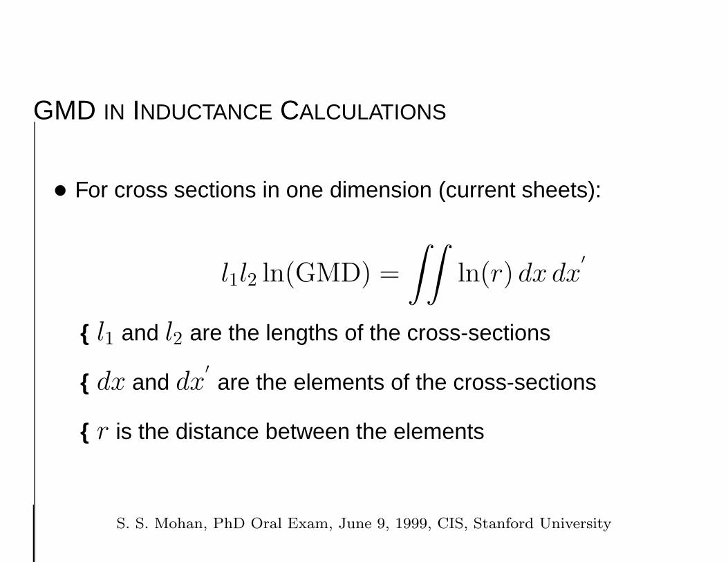
PARALLEL LINES OF EQUAL LENGTH
l
R
M ≈ µl
2π
[ln(2l) − ln(R) − 1 +
R
l− R2
4l2
]for
(R
l
)≤ 1
S. S. Mohan, PhD Oral Exam, June 9, 1999, CIS, Stanford University

INDUCTANCE OF CURRENT SHEET
l
R
M =µl
2π
[ln(2l) − ln(R) − 1 +
R
l− R2
4l2
]
Ls =µl
2π
[ln(2l) − ln(GMD) − 1 +
AMD
l− AMSD2
4l2
]
S. S. Mohan, PhD Oral Exam, June 9, 1999, CIS, Stanford University

INDUCTANCE OF RECTANGULAR CURRENT SHEET
l I
w2
w2
x1 x2
−w
2< x1, x2 <
w
2
ln (GMD) = ln |x1 + x2| = ln w − 1.5
AMD = |x1 + x2| =w
3
AMSD2 = (x1 + x2)2 =w2
6
L =µl
2π
[ln
(2l
w
)+ 0.5 +
w
3l− w2
24l2
]
S. S. Mohan, PhD Oral Exam, June 9, 1999, CIS, Stanford University

EQUIVALENT RECTANGULAR CURRENT SHEET
...ll
IIII
wwww ss
nI
ρl = nw + (n − 1)s
1 2 (n−1) n
L =µn2l
2π
[ln
(2
ρ
)+ 0.5 +
ρ
3− ρ2
24
]
S. S. Mohan, PhD Oral Exam, June 9, 1999, CIS, Stanford University

APPROXIMATING A SQUARE SPIRAL
davg
w
s
nI
dout = (1 + ρ)davg
ρdavg
S. S. Mohan, PhD Oral Exam, June 9, 1999, CIS, Stanford University

ONE SIDE OF A SQUARE SPIRAL: Ls
...
davg davg
II
I
I
wwww ss
nI
ρdavg = nw + (n − 1)s
12
(n−1)n
S. S. Mohan, PhD Oral Exam, June 9, 1999, CIS, Stanford University

OPPOSITE SIDES OF A SQUARE SPIRAL: Mopp
davg
davg
nI
nI
ρdavg
ρdavg
90o
90o
S. S. Mohan, PhD Oral Exam, June 9, 1999, CIS, Stanford University

CURRENT SHEET EXPRESSION FOR A SQUARE SPIRAL
davg
nInI
nI
nI
ρdavg
ρdavg
90o
90o
Lsq = 4(Ls + Mopp)
=2µn2davg
π
[ln
(2.067
ρ
)+ 0.178ρ + 0.125ρ2
]
S. S. Mohan, PhD Oral Exam, June 9, 1999, CIS, Stanford University

CONCENTRIC CIRCULAR CONDUCTORS
...
I
I
I
www
s
ddnI
ρdavg =nw+(n−1)s1 2 n
L ≈ µn2davg
2
[ln
(1
ρ
)+ 0.9 + 0.2ρ2
]
S. S. Mohan, PhD Oral Exam, June 9, 1999, CIS, Stanford University

CURRENT SHEET EXPRESSIONS
Lcursh =µn2davgc1
2
[ln(c2/ρ) + c3ρ + c4ρ
2]
Layout c1 c2 c3 c4
Square 1.27 2.07 0.18 0.13
Hexagonal 1.09 2.23 0.00 0.17
Octagonal 1.07 2.29 0.00 0.19
Circle 1.00 2.46 0.00 0.20
S. S. Mohan, PhD Oral Exam, June 9, 1999, CIS, Stanford University

OTHER INDUCTANCE EXPRESSIONS
• Monomial Expression :
Lmon = βdα1outw
α2dα3avgn
α4sα5
• Modified Wheeler Expression :
Lmw = K1µ0n2davg
1 + K2ρ
S. S. Mohan, PhD Oral Exam, June 9, 1999, CIS, Stanford University

COMPARISON TO FIELD SOLVERS: PREVIOUS WORK
CrolsVoormanBryanRonDill
00
20
20
40
40
60
60
80
80
100
% Absolute error
%In
duct
ors
exce
edin
gab
s.er
ror
Min Max
L(nH) 0.1 70
OD(µm) 100 400
n 1 20
s/w 0.02 3
ρ 0.03 0.95
19, 000 simulations
S. S. Mohan, PhD Oral Exam, June 9, 1999, CIS, Stanford University

COMPARISON TO FIELD SOLVERS: NEW WORK
Current SheetMonomial FitModified Wheeler
2 4 6 8 10 1200
20
40
60
80
100
% Absolute error
%In
duct
ors
exce
edin
gab
s.er
ror
Min Max
L(nH) 0.1 70
OD(µm) 100 400
n 1 20
s/w 0.02 3
ρ 0.03 0.95
19, 000 simulations
S. S. Mohan, PhD Oral Exam, June 9, 1999, CIS, Stanford University

EXPERIMENTAL SET-UP
S parameters
DUT
Coplanar GSG probes
HP8720B
network analyzer
50Ω environment
port 1 port 2
S. S. Mohan, PhD Oral Exam, June 9, 1999, CIS, Stanford University

COMPARISON TO EXPERIMENTS: PREVIOUS WORK
CrolsVoormanBryanRonDill
00
20
20
40
40
60
60
80
80
100
% Absolute error
%In
duct
ors
exce
edin
gab
s.er
ror
S. S. Mohan, PhD Oral Exam, June 9, 1999, CIS, Stanford University

COMPARISON TO EXPERIMENTS: NEW WORK
ASITICCurrent SheetModified WheelerMonomial Fit
4 8 12 1600
20
20
40
60
80
100
% Absolute error
%In
duct
ors
exce
edin
gab
s.er
ror
S. S. Mohan, PhD Oral Exam, June 9, 1999, CIS, Stanford University

PARAMETERS OF INTEREST
• Inductor quality factor (QL)
QL = 2π[peak magnetic energy − peak electric energy]
energy loss in one oscillation cycle
• Tank quality factor (Qtank)
Qtank = 2πpeak magnetic energy
energy loss in one oscillation cycle
• Self-resonance frequency (ωres), frequency at which QL = 0
S. S. Mohan, PhD Oral Exam, June 9, 1999, CIS, Stanford University

EXAMPLE: MAXIMUM QL @ 2GHz FOR L = 8nH
SquareHexagonalOctagonalCircular1
1
2
2
3
3
4
40
0
5
6Q
L
Frequency (GHz)
S. S. Mohan, PhD Oral Exam, June 9, 1999, CIS, Stanford University

EXAMPLE: SHUNT-PEAKED AMPLIFIER
Common Source Amplifier
R
C
Vdd
vout
vin
Shunt-peaked Amplifier
L
R
C
Vdd
vout
vin
• Bandwidth enhancement using zeros
• No additional power dissipation
S. S. Mohan, PhD Oral Exam, June 9, 1999, CIS, Stanford University

ON-CHIP SHUNT PEAKING
Vdd
L
(R − Rs)
Rs
vout
vin
Cg
CL
Cd Cload
• Work with inductor parasitics
• Rs is not an issue(now part of load resistance)
• Inductor Q is not relevant
• Minimize area and CL
• L determined byR, Cload, CL and Cd
S. S. Mohan, PhD Oral Exam, June 9, 1999, CIS, Stanford University

SHUNT-PEAKED TRANSIMPEDANCE AMPLIFIER
Vdd
L
(R − Rs)
Rs
Rf
vout
iin Cin Cg
CL
Cd Cload
• Input current drive
• Cascode stage
• On-chip shunt-peaking
• Feedback
S. S. Mohan, PhD Oral Exam, June 9, 1999, CIS, Stanford University

DESIGN METHODOLOGY
1. Design and optimize transimpedance stagewithout shunt peaking
2. Transistor current determines conductor width, w
3. Lithography sets spacing, s
4. Choose n and AD to realize desired Lwhile minimizing parasitic capacitance and area
5. Maximize transimpedance resistance, Rf
S. S. Mohan, PhD Oral Exam, June 9, 1999, CIS, Stanford University
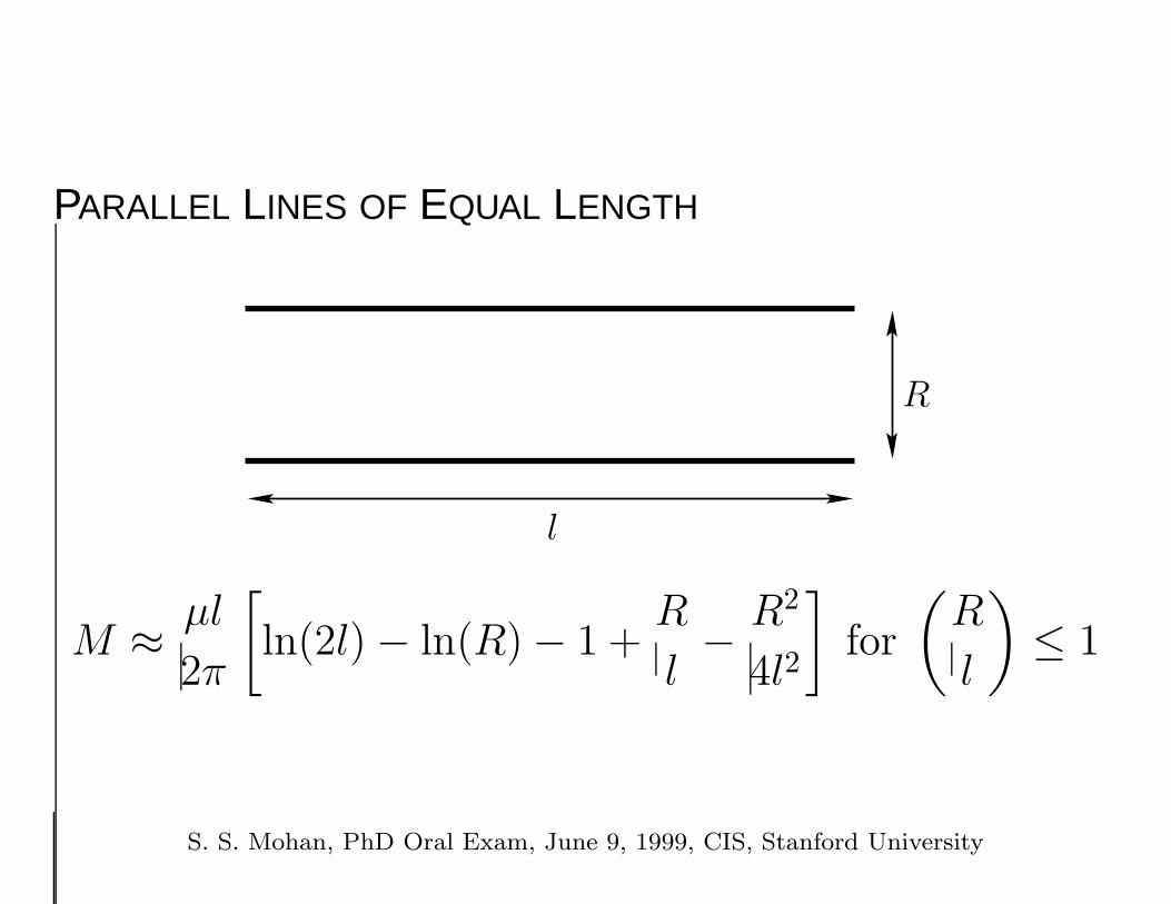
TRANSFORMER
i1 i2v1 v2
+ +
− −L1 L2
M
• v1 = L1∂i1∂t
+ M ∂i2∂t
v2 = L2∂i2∂t
+ M ∂i1∂t
• Mutual coupling coefficient, k = M√L1L2
• |k| ≤ 1
S. S. Mohan, PhD Oral Exam, June 9, 1999, CIS, Stanford University

NON-IDEAL TRANSFORMER
L1 L2
MR1 R2
• k = M√L1L2
< 1.
• Series resistance.
• Port-to-port & port-to-substrate capacitances
S. S. Mohan, PhD Oral Exam, June 9, 1999, CIS, Stanford University

TAPPED TRANSFORMER
Inner
spiral
Outer spiral
• advantages: High L1, L2
Top metal layer
Low port-to-portcapacitance
• disadvantages:
Asymmetric
Low k(≈ 0.3 − 0.5)
S. S. Mohan, PhD Oral Exam, June 9, 1999, CIS, Stanford University

INTERLEAVED TRANSFORMER
Primary Secondary
• advantages: Medium k
(≈ 0.7 − 0.8)
Symmetric
Top metal layer
• disadvantages:
Medium port-to-portcapacitance
Low L1, L2
S. S. Mohan, PhD Oral Exam, June 9, 1999, CIS, Stanford University
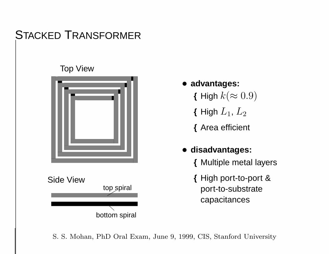
STACKED TRANSFORMER
Top View
Side Viewtop spiral
bottom spiral
• advantages: High k(≈ 0.9)
High L1, L2
Area efficient
• disadvantages:
Multiple metal layers
High port-to-port &port-to-substratecapacitances
S. S. Mohan, PhD Oral Exam, June 9, 1999, CIS, Stanford University

STACKED TRANSFORMER VARIATIONS
Bottom spiral Top spiral
xs xs
ys
ds
• Shift top and bottom spirals laterally or diagonally
• Trade-off lower k for reduced port-to-port capacitance
S. S. Mohan, PhD Oral Exam, June 9, 1999, CIS, Stanford University

COMPARISON OF TRANSFORMER REALIZATIONS
Transformer Area Coupling Self- Self-resonant
type coefficient, k inductance frequency
Tapped High Low Mid High
Interleaved High Mid Low High
Stacked Low High High Low
• Non-idealities result in trade-offs
• Optimal choice determined by circuit application
• Transformer models needed for comparison
S. S. Mohan, PhD Oral Exam, June 9, 1999, CIS, Stanford University

TAPPED TRANSFORMER MODEL
Cov,o
Cox,o
Cox,i
Rs,o
Rs,i
Ls,o
Ls,i
M
Port1
Port2
(inner)Ls,i
Ls,o (outer)
• Evaluate Cov,o, Cox,o, Cox,i,Rs,o & Rs,i by extendingprevious work
• Use inductance expression forLs,o, Ls,i
• Calculate M
S. S. Mohan, PhD Oral Exam, June 9, 1999, CIS, Stanford University

MUTUAL INDUCTANCE CALCULATION
Single inductor.
LT
Interleaved transformer.
L1(primary) L2 (secondary)
Tapped transformer.
(inner)L1
L2 (outer)
• LT = L1 + L2 + 2M
S. S. Mohan, PhD Oral Exam, June 9, 1999, CIS, Stanford University

STACKED TRANSFORMER MODEL
Cov
Cox,t
Coxm
Cox,b
Rs,t
Rs,b
Ls,t
Ls,b
M
Port1
Port2
xs
ys
• Evaluate Cov, Cox,t, Coxm,Cox,b, Rs,t & Rs,b by extendingprevious work
• Use inductanceexpression for Ls,t, Ls,b
• Calculate M
S. S. Mohan, PhD Oral Exam, June 9, 1999, CIS, Stanford University

CURRENT SHEET APPROACH FOR k
xsxs
ysys
dsds
• Reduce complexity by 4n2
• Use symmetry
• Derive simple expression using electromagnetic theory
S. S. Mohan, PhD Oral Exam, June 9, 1999, CIS, Stanford University

k FOR STACKED TRANSFORMERS
0.00.2
0.2
0.4
0.4
0.6
0.6
0.8
1.0
predicted kmeasured k
Mut
ualC
oupl
ing
Coe
ffici
ent(
k)
dnorm =
√xs
2+ys2
AD = ds
AD
k ≈ (0.9 − dnorm)(for k > 0.2)
xs
ysds
Ls,t
Ls,b
M = k√
(Ls,tLs,b)
• Metal and oxide thicknesses have only 2nd order effects on k
S. S. Mohan, PhD Oral Exam, June 9, 1999, CIS, Stanford University

EXPERIMENTAL SET-UP
S parameters
DUT
Coplanar GSG probes
HP8720Bnetwork analyzer
50Ω environment
port 1 port 2
port 3
L1
L1
L2
L2
M
M
port 1
port 1
port 2
port 2
port 3
port 3
S. S. Mohan, PhD Oral Exam, June 9, 1999, CIS, Stanford University
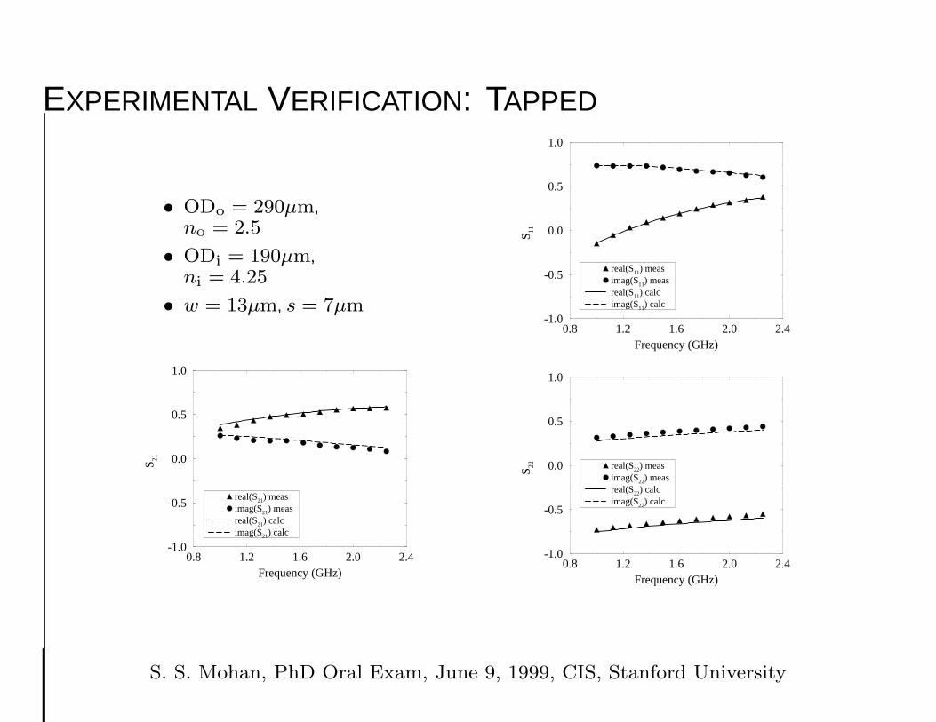
EXPERIMENTAL VERIFICATION: TAPPED
• ODo = 290µm,no = 2.5
• ODi = 190µm,ni = 4.25
• w = 13µm, s = 7µm
0.8 1.2 1.6 2.0 2.4Frequency (GHz)
-1.0
-0.5
0.0
0.5
1.0
S 21
real(S21) measimag(S21) measreal(S21) calcimag(S21) calc
0.8 1.2 1.6 2.0 2.4Frequency (GHz)
-1.0
-0.5
0.0
0.5
1.0
S 11
real(S11) measimag(S11) measreal(S11) calcimag(S11) calc
0.8 1.2 1.6 2.0 2.4Frequency (GHz)
-1.0
-0.5
0.0
0.5
1.0
S 22 real(S22) measimag(S22) measreal(S22) calcimag(S22) calc
S. S. Mohan, PhD Oral Exam, June 9, 1999, CIS, Stanford University

EXPERIMENTAL VERIFICATION: STACKED 1
• Stacked transformer withtop spiral overlapping bot-tom one
• OD = 180µm, n = 11.75,w = 3.2µm, s = 2.1µm
• xs = 0µm, ys = 0µm,ds = 0µm
0.0 0.5 1.0 1.5Frequency (GHz)
-1.0
-0.5
0.0
0.5
1.0
S 21
real(S21) measimag(S21) measreal(S21) calcimag(S21) calc
0.0 0.5 1.0 1.5Frequency (GHz)
-1.0
-0.5
0.0
0.5
1.0
S 11
real(S11) measimag(S11) measreal(S11) calcimag(S11) calc
0.0 0.5 1.0 1.5Frequency (GHz)
-1.0
-0.5
0.0
0.5
1.0
S 22
real(S22) measimag(S22) measreal(S22) calcimag(S22) calc
S. S. Mohan, PhD Oral Exam, June 9, 1999, CIS, Stanford University

FUTURE WORK
• Incorporate inductive coupling to substrate:significant in CMOS epi processes
• Improve expressions for the series resistanceto include proximity effects
• Extend current sheet approachto handle non-uniform current distributions
S. S. Mohan, PhD Oral Exam, June 9, 1999, CIS, Stanford University

CONTRIBUTIONS
• Current sheet approach to inductance calculation
• Simple accurate expression for inductance ofsdquare, hexagonal, octagonal and circular spirals
• Expressions for mutual inductance andmutual coupling coefficient
• On-chip transformer models
• Basis for design and synthesis ofon-chip inductor and transformer circuits
• Shunt-peaked amplifier with optimized on-chip inductor
S. S. Mohan, PhD Oral Exam, June 9, 1999, CIS, Stanford University

SO WHAT ?
• Design
Scalable, analytical models forsynthesis and optimization
• Verification
Field solvers
S. S. Mohan, PhD Oral Exam, June 9, 1999, CIS, Stanford University