Embed Size (px)
Citation preview
Overcurrent Protection:
Reference Design & Study
ECE 480
Design Team 5
Kenji Aono
Stephen England
Ryan Laderach
Joshua Myers
Facilitator: Dr. Wen Li
Sponsor Representative: Mr. Pete Semig

Overview of Project
• What is over-current protection?
– Traditional methods
– Advantages
Introduction
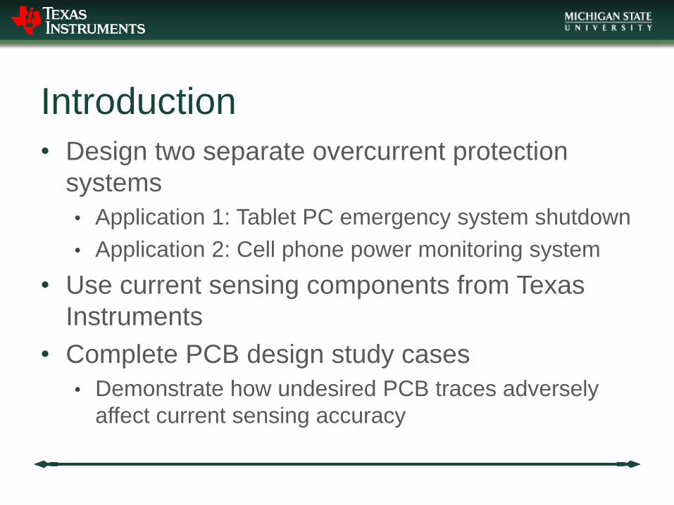
• Design two separate overcurrent protection
systems
• Application 1: Tablet PC emergency system shutdown
• Application 2: Cell phone power monitoring system
• Use current sensing components from Texas
Instruments
• Complete PCB design study cases
• Demonstrate how undesired PCB traces adversely
affect current sensing accuracy

Design Specifications
• Application 1
• Assume 3.6 V, 6.75 A-hr Li-Ion battery
• Shutdown at 1 A
• Priorities
1. Small size
2. Low cost
3. Low power consumption
4. Fast speed of shutoff

Final Design & Results
• Application 1 Design

Final Design & Results
Application 1 Results
Switches off at 2.5 V
Speed: 750 µs
(SN74LS74)
SN74LS74 .97in X .75in 7.58mA 27.288mW
SN74AUP1G80 1.01in X .529in 3.83mA 13.788mW

Final Design & Results • Application 1 Alternative Design
Final Design & Results
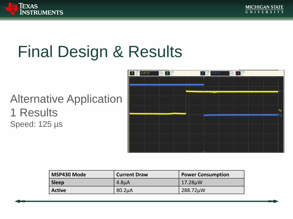
Alternative Application
1 Results Speed: 125 µs
MSP430 Mode Current Draw Power Consumption
Sleep 4.8µA 17.28µW
Active 80.2µA 288.72µW
Design Specifications
• Application 2
• Well regulated 3V supply voltage
• Variable load: 2.7V-3.3V
• Accurate between 7mA-192.5mA
• Priorities
1. Minimal system impact
2. Small size
3. High accuracy

Final Design & Results
• Application 2 Design
Cell phone

Final Design & Results
Application 2 Software Results
Initialize Microcontroller
Connect With LCD
Display Results
Begin ADC Process

Final Design & Results
Application 2 Demonstration

Design Challenges & Recommendations
• Printed Circuit Boards (PCBs)
• Necessary for testing all design iterations
• Professional fabrication methods are high cost and
provide slow turnaround
• Requires a quick, cheap method
• CNC milling provided by ECE department ineffective
for our designs
PCB Design and Fabrication
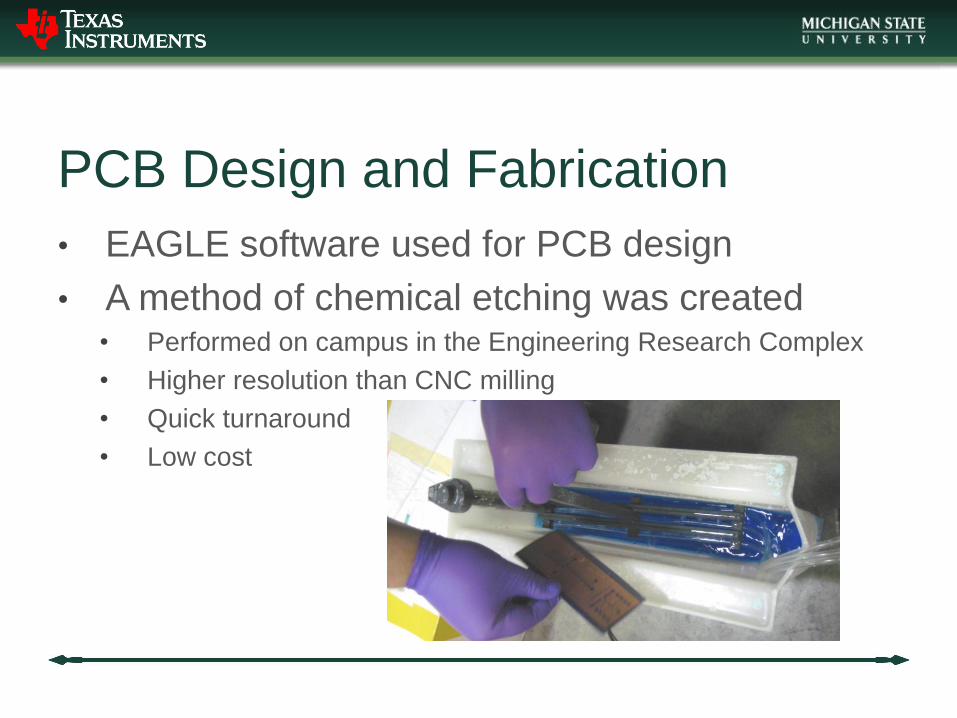
• EAGLE software used for PCB design
• A method of chemical etching was created • Performed on campus in the Engineering Research Complex
• Higher resolution than CNC milling
• Quick turnaround
• Low cost

PCB Design Study Results
• Four cases tested
• Ideal trace
• Long distance traces
• Non-symmetrical traces
• Non-Kelvin connection
traces

PCB Design Study Results
*Results with 30Ω load (100mA current draw)
Case Current Expected output Output %Error
Ideal 118.92mA 297.3mV 323.5mV 8.81%
Long 111.42mA 278.55mV 493.89mV 77.31%
Non-symmetrical 100.24mA 250.56mV 273.77mV 9.57%
Non-Kelvin 99.513mA 248.78mV 325.24mV 30.77%

Conclusions • Application One
– Low cost
– Reasonably fast shutoff speed
– Accurate
– Minimal size with given resources
• Application Two
– Precise
– Small size
– Minimal impact

Future Suggestions
• Use MSP430 for application one
• Solve soldering issues of MSP430 and other
small components
• Higher budget

Questions