Embed Size (px)
Citation preview
1/38
GP2Y0E02A,GP2Y0E02B,GP2Y0E03GP2Y0E02A,GP2Y0E02B,GP2Y0E03GP2Y0E02A,GP2Y0E02B,GP2Y0E03GP2Y0E02A,GP2Y0E02B,GP2Y0E03 Application NoteApplication NoteApplication NoteApplication Note
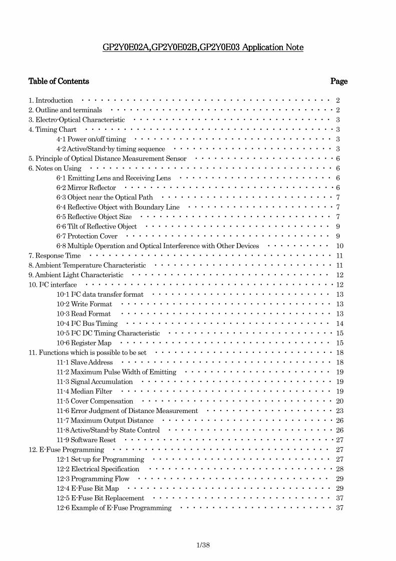
Table of ContentsTable of ContentsTable of ContentsTable of Contents PPPPageageageage
1. Introduction ・・・・・・・・・・・・・・・・・・・・・・・・・・・・・・・・・・・・・・・ 2
2. Outline and terminals ・・・・・・・・・・・・・・・・・・・・・・・・・・・・・・・・・・・ 2
3. Electro-Optical Characteristic ・・・・・・・・・・・・・・・・・・・・・・・・・・・・・・・ 3
4. Timing Chart ・・・・・・・・・・・・・・・・・・・・・・・・・・・・・・・・・・・・・・・ 3
4-1 Power on/off timing ・・・・・・・・・・・・・・・・・・・・・・・・・・・・・・・ 3
4-2 Active/Stand-by timing sequence ・・・・・・・・・・・・・・・・・・・・・・・・・ 3
5. Principle of Optical Distance Measurement Sensor ・・・・・・・・・・・・・・・・・・・・・・ 6
6. Notes on Using ・・・・・・・・・・・・・・・・・・・・・・・・・・・・・・・・・・・・・・ 6
6-1 Emitting Lens and Receiving Lens ・・・・・・・・・・・・・・・・・・・・・・・・ 6
6-2 Mirror Reflector ・・・・・・・・・・・・・・・・・・・・・・・・・・・・・・・・・ 6
6-3 Object near the Optical Path ・・・・・・・・・・・・・・・・・・・・・・・・・・・ 7
6-4 Reflective Object with Boundary Line ・・・・・・・・・・・・・・・・・・・・・・・ 7
6-5 Reflective Object Size ・・・・・・・・・・・・・・・・・・・・・・・・・・・・・・ 7
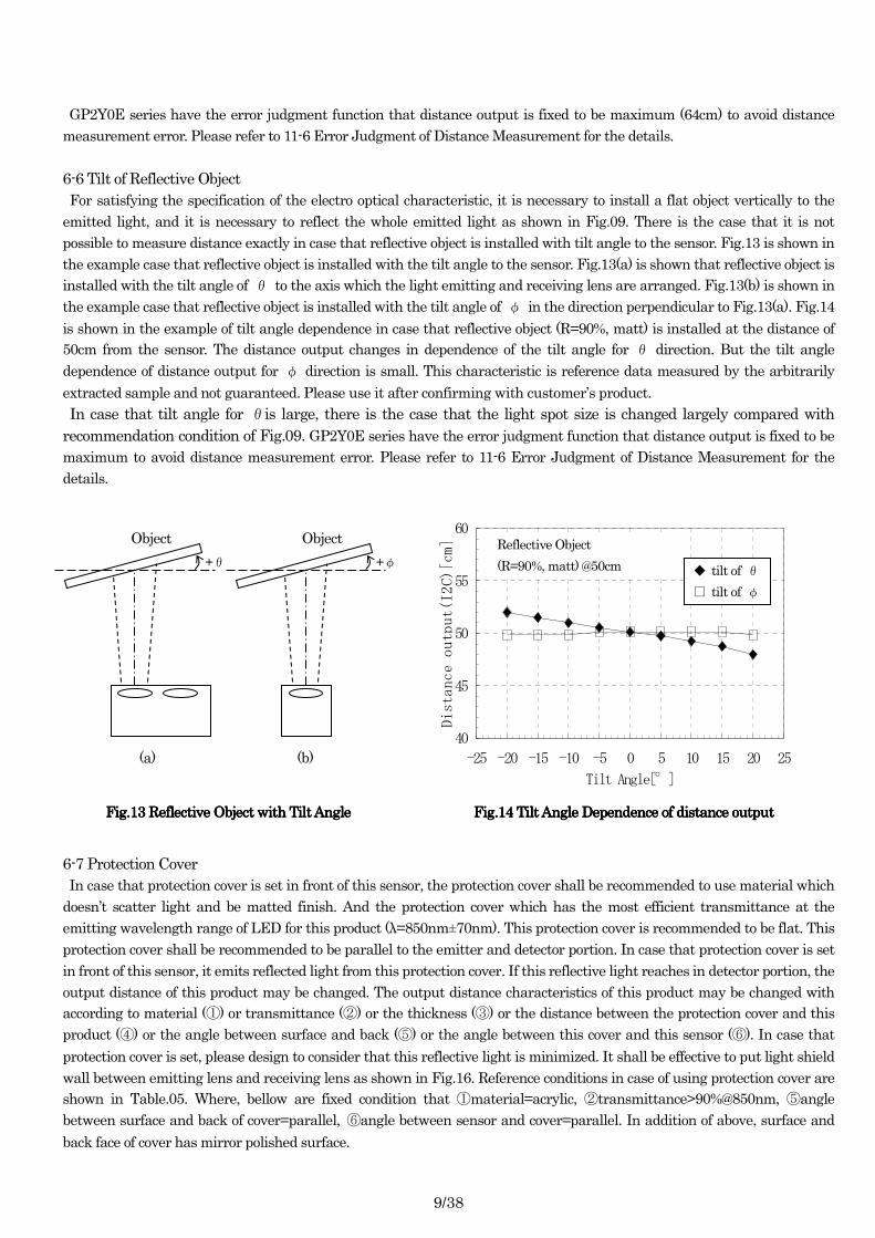
6-6 Tilt of Reflective Object ・・・・・・・・・・・・・・・・・・・・・・・・・・・・・ 9
6-7 Protection Cover ・・・・・・・・・・・・・・・・・・・・・・・・・・・・・・・・ 9
6-8 Multiple Operation and Optical Interference with Other Devices ・・・・・・・・・・ 10
7. Response Time ・・・・・・・・・・・・・・・・・・・・・・・・・・・・・・・・・・・・・・ 11
8. Ambient Temperature Characteristic ・・・・・・・・・・・・・・・・・・・・・・・・・・・・ 11
9. Ambient Light Characteristic ・・・・・・・・・・・・・・・・・・・・・・・・・・・・・・・ 12
10. I2C interface ・・・・・・・・・・・・・・・・・・・・・・・・・・・・・・・・・・・・・・・ 12
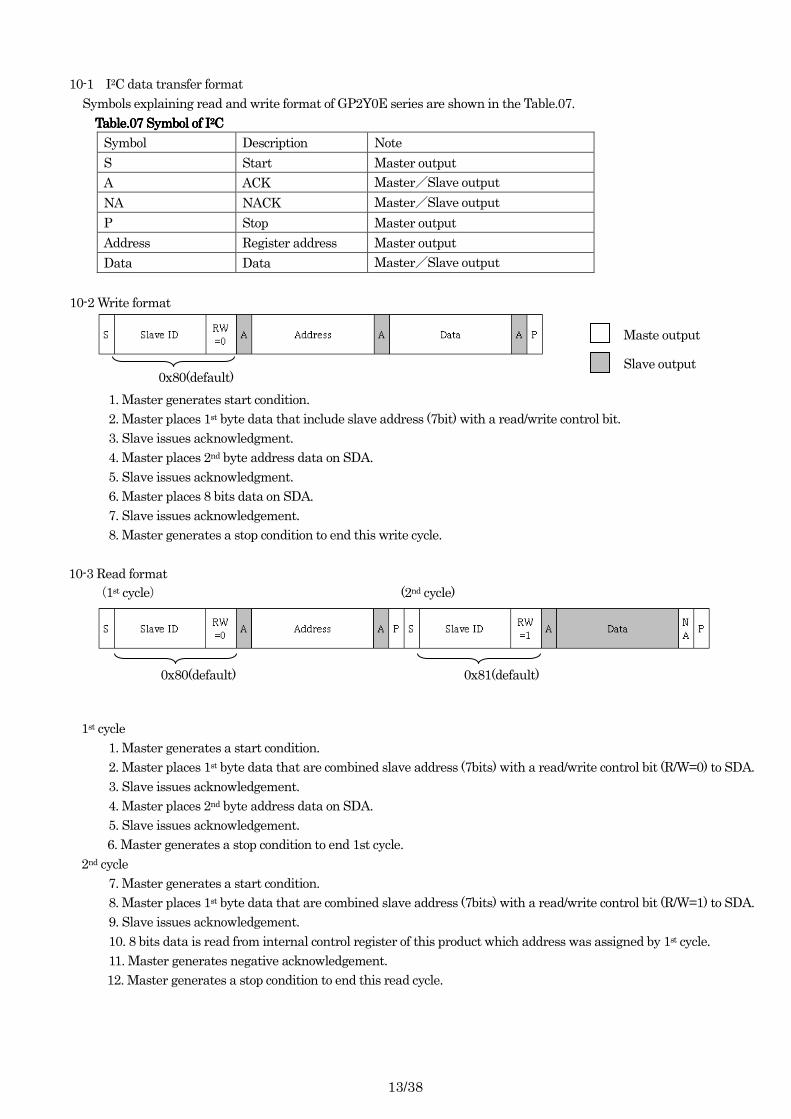
10-1 I2C data transfer format ・・・・・・・・・・・・・・・・・・・・・・・・・・・・ 13
10-2 Write Format ・・・・・・・・・・・・・・・・・・・・・・・・・・・・・・・・・ 13
10-3 Read Format ・・・・・・・・・・・・・・・・・・・・・・・・・・・・・・・・・ 13
10-4 I2C Bus Timing ・・・・・・・・・・・・・・・・・・・・・・・・・・・・・・・・ 14
10-5 I2C DC Timing Characteristic ・・・・・・・・・・・・・・・・・・・・・・・・・・ 15
10-6 Register Map ・・・・・・・・・・・・・・・・・・・・・・・・・・・・・・・・・ 15
11. Functions which is possible to be set ・・・・・・・・・・・・・・・・・・・・・・・・・・・・ 18
11-1 Slave Address ・・・・・・・・・・・・・・・・・・・・・・・・・・・・・・・・・ 18
11-2 Maximum Pulse Width of Emitting ・・・・・・・・・・・・・・・・・・・・・・・ 19
11-3 Signal Accumulation ・・・・・・・・・・・・・・・・・・・・・・・・・・・・・・ 19
11-4 Median Filter ・・・・・・・・・・・・・・・・・・・・・・・・・・・・・・・・・ 19
11-5 Cover Compensation ・・・・・・・・・・・・・・・・・・・・・・・・・・・・・・ 20
11-6 Error Judgment of Distance Measurement ・・・・・・・・・・・・・・・・・・・・ 23
11-7 Maximum Output Distance ・・・・・・・・・・・・・・・・・・・・・・・・・・・ 26
11-8 Active/Stand-by State Control ・・・・・・・・・・・・・・・・・・・・・・・・・・ 26
11-9 Software Reset ・・・・・・・・・・・・・・・・・・・・・・・・・・・・・・・・・ 27
12. E-Fuse Programming ・・・・・・・・・・・・・・・・・・・・・・・・・・・・・・・・・・ 27
12-1 Set-up for Programming ・・・・・・・・・・・・・・・・・・・・・・・・・・・・ 27
12-2 Electrical Specification ・・・・・・・・・・・・・・・・・・・・・・・・・・・・・ 28
12-3 Programming Flow ・・・・・・・・・・・・・・・・・・・・・・・・・・・・・・ 29
12-4 E-Fuse Bit Map ・・・・・・・・・・・・・・・・・・・・・・・・・・・・・・・・ 29
12-5 E-Fuse Bit Replacement ・・・・・・・・・・・・・・・・・・・・・・・・・・・・ 37
12-6 Example of E-Fuse Programming ・・・・・・・・・・・・・・・・・・・・・・・・ 37
2/38
1. Introduction
The GP2Y0E series are active optical distance measurement sensors. These sensors measure the distance to an object by
detecting the light spot position of reflection on the detector. It is possible to measure the distance with high accuracy by
adoption of CMOS image sensor. It is not necessary for the customer to calibrate the distance output. The three models have
differing output types and operating voltages. The differences are shown in table.01.
Table.01Table.01Table.01Table.01 the list of GP2Y0E seriesthe list of GP2Y0E seriesthe list of GP2Y0E seriesthe list of GP2Y0E series
Distance output Terminals VDD Detection range
GP2Y0E02A Analog 4 2.7~3.3V 4~50cm
GP2Y0E02B Digital(I2C bus) 4 2.7~3.3V 4~50cm
GP2Y0E03 Analog
Digital(I2C bus)
7 2.7~5.5V
(*)
4~50cm
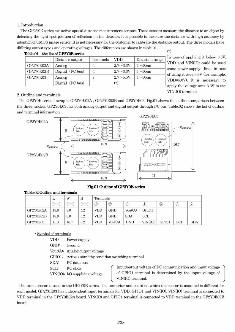
2. Outline and terminals
The GP2Y0E series line-up is GP2Y0E02A , GP2Y0E02B and GP2Y0E03. Fig.01 shows the outline comparison between
the three models. GP2Y0E03 has both analog output and digital output through I2C bus. Table.02 shows the list of outline
and terminal information.
Fig.01 Outline of GP2Y0E seriesFig.01 Outline of GP2Y0E seriesFig.01 Outline of GP2Y0E seriesFig.01 Outline of GP2Y0E series
Table.02Table.02Table.02Table.02 Outline and terminalsOutline and terminalsOutline and terminalsOutline and terminals
L
[mm]
W
[mm]
H
[mm]
Terminals
① ② ③ ④ ⑤ ⑥ ⑦
GP2Y0E02A 18.9 8.0 5.2 VDD GND Vout(A) GPIO1 - - -
GP2Y0E02B 18.9 8.0 5.2 VDD GND SDA SCL - - -
GP2Y0E03 11.0 16.7 5.2 VDD Vout(A) GND VIN(IO) GPIO1 SCL SDA
・Symbol of terminals
VDD: Power supply
GND: Ground
Vout(A): Analog output voltage
GPIO1: Active / stand-by condition switching terminal
SDA: I2C data bus
SCL: I2C clock
VIN(IO): I/O supplying voltage
The same sensor is used in the GP2Y0E series. The connector and board on which the sensor is mounted is different for
each model. GP2Y0E03 has independent input terminals for VDD, GPIO1 and VIN(IO). VIN(IO) terminal is connected to
VDD terminal in the GP2Y0E02A board. VIN(IO) and GPIO1 terminal is connected to VDD terminal in the GP2Y0E02B
board.
Input/output voltage of I2C communication and input voltage
of GPIO1 terminal is determined by the input voltage of
VIN(IO) terminal.
GP2Y0E02A
GP2Y0E02B
GP2Y0E03
11
16.7
8
8
18.9
18.9
①
④
②
①②③④⑤⑥⑦
③
①
④
②
③
Sensor
Sensor Emitter Side
Receiver Side
Emitter Side
Receiver Side
Emitter Side
Receiver Side
(*)
In case of applying it below 3.3V,
VDD and VIN(IO) could be used
same power supply line. .In case
of using it over 3.6V (for example,
VDD=5.0V), it is necessary to
apply the voltage over 3.3V to the
VIN(IO) terminal.
3/38
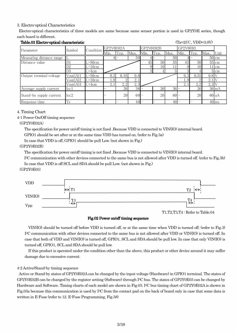
3. Electro-optical Characteristics
Electro-optical characteristics of three models are same because same sensor portion is used in GP2Y0E series, though
each board is different.
Table.03 ElectroTable.03 ElectroTable.03 ElectroTable.03 Electro----optical characteristicoptical characteristicoptical characteristicoptical characteristic (Ta=25℃, VDD=3.0V)
4. Timing Chart
4-1 Power On/Off timing sequence
(GP2Y0E02A)
The specification for power on/off timing is not fixed .Because VDD is connected to VIN(IO) internal board.
GPIO1 should be set after or at the same time VDD has turned on. (refer to Fig.3a)
In case that VDD is off, GPIO1 should be pull Low. (not shown in Fig.)
(GP2Y0E02B)
The specification for power on/off timing is not fixed .Because VDD is connected to VIN(IO) internal board.
I2C communication with other devices connected to the same bus is not allowed after VDD is turned off. (refer to Fig.3b)
In case that VDD is off SCL and SDA should be pull Low. (not shown in Fig.)
(GP2Y0E03)
VIN(IO) should be turned off before VDD is turned off, or at the same time when VDD is turned off. (refer to Fig.3)
I2C communication with other devices connected to the same bus is not allowed after VDD or VIN(IO) is turned off. In
case that both of VDD and VIN(IO) is turned off, GPIO1, SCL and SDA should be pull low. In case that only VIN(IO) is
turned off, GPIO1, SCL and SDA should be pull low.
If this product is operated under the condition other than the above, this product or other device around it may suffer
damage due to excessive current.
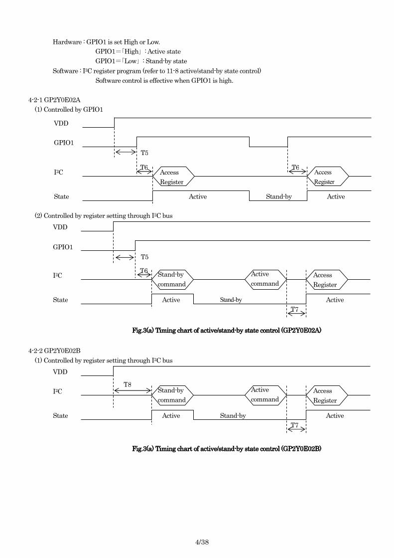
4-2 Active/Stand-by timing sequence
Active or Stand-by states of GP2Y0E02A can be changed by the input voltage (Hardware) in GPIO1 terminal. The states of
GP2Y0E02B can be changed by the register setting (Software) through I2C bus. The states of GP2Y0E03 can be changed by
Hardware and Software. Timing charts of each model are shown in Fig.03. I2C bus timing chart of GP2Y0E02A is shown in
Fig.03a because this communication is used by I2C from the contact pad on the back of board only in case that some data is
written in E-Fuse (refer to 12. E-Fuse Programming, Fig.38)
VDD
VIN(IO)
T1 T2
T1,T2,T3,T4 : Refer to Table.04
GP2Y0E02A GP2Y0E02B GP2Y0E03Min. Typ. Max. Min. Typ. Max. Min. Typ. Max. Unit
Measuring distance range L 4 - 50 4 - 50 4 - 50 cmDistance value D1 L=50cm 45 50 55 45 50 55 cm
D2 L=10cm 9 10 11 9 10 11 cmD3 L=4cm 3 4 5 3 4 5 cmVout(A)1 L=50cm 0.3 0.55 0.8 0.3 0.55 0.8 VVout(A)2 L=10cm 1.9 2 2.1 1.9 2 2.1 VVout(A)3 L=4cm 2.1 2.2 2.3 2.1 2.2 2.3 V
Average supply current Icc1 - 26 36 - 26 36 - 26 36 mA
Stand-by supply current Icc2 - 20 60 - 20 60 - 20 60 uA
Response time Ts - - 40 - - 40 - - 40 ms
Output terminal voltage
Parameter Symbol Condition
T3 Vpp
T4
Fig.02 Power on/off timing sequenceFig.02 Power on/off timing sequenceFig.02 Power on/off timing sequenceFig.02 Power on/off timing sequence
4/38
Hardware : GPIO1 is set High or Low.
GPIO1=「High」 : Active state
GPIO1=「Low」 : Stand-by state
Software : I2C register program (refer to 11-8 active/stand-by state control)
Software control is effective when GPIO1 is high.
4-2-1 GP2Y0E02A
(1) Controlled by GPIO1
(2) Controlled by register setting through I2C bus
4-2-2 GP2Y0E02B
(1) Controlled by register setting through I2C bus
VDD
GPIO1
T5
Access
Register
I2C Access
Register
T6 T6
Active State Stand-by Active
VDD
GPIO1
Stand-by
command I2C Access
Register
T6
T7
Active State Stand-by Active
Active
command
T5
Fig.3(a) Timing chart of active/standFig.3(a) Timing chart of active/standFig.3(a) Timing chart of active/standFig.3(a) Timing chart of active/stand----by state control (GP2Y0E02A)by state control (GP2Y0E02A)by state control (GP2Y0E02A)by state control (GP2Y0E02A)
VDD
Stand-by
command I2C Access
Register
T8
T7
Active State Stand-by Active
Active
command
Fig.3(a) Timing chart of active/standFig.3(a) Timing chart of active/standFig.3(a) Timing chart of active/standFig.3(a) Timing chart of active/stand----by state control (GP2Y0E02B)by state control (GP2Y0E02B)by state control (GP2Y0E02B)by state control (GP2Y0E02B)
5/38
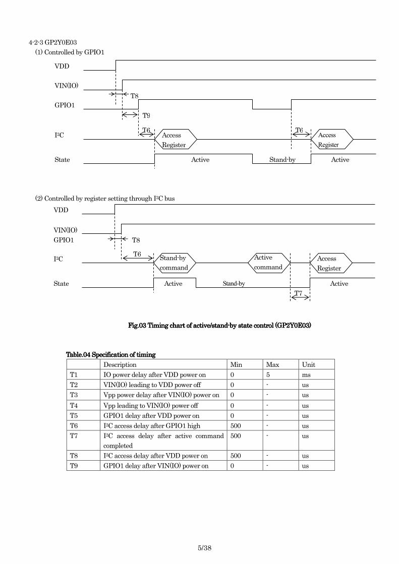
4-2-3 GP2Y0E03
(1) Controlled by GPIO1
(2) Controlled by register setting through I2C bus
Fig.03 Timing chart of active/standFig.03 Timing chart of active/standFig.03 Timing chart of active/standFig.03 Timing chart of active/stand----by state controlby state controlby state controlby state control (GP2Y0E03)(GP2Y0E03)(GP2Y0E03)(GP2Y0E03)
Table.04 Specification of timingTable.04 Specification of timingTable.04 Specification of timingTable.04 Specification of timing
Description Min Max Unit
T1 IO power delay after VDD power on 0 5 ms
T2 VIN(IO) leading to VDD power off 0 - us
T3 Vpp power delay after VIN(IO) power on 0 - us
T4 Vpp leading to VIN(IO) power off 0 - us
T5 GPIO1 delay after VDD power on 0 - us
T6 I2C access delay after GPIO1 high 500 - us
T7 I2C access delay after active command
completed
500 - us
T8 I2C access delay after VDD power on 500 - us
T9 GPIO1 delay after VIN(IO) power on 0 - us
VDD
VIN(IO)
T8
GPIO1
T9
Access
Register
I2C Access
Register
T6 T6
Active State Stand-by Active
VDD
VIN(IO)
GPIO1
Stand-by
command I2C Access
Register
T6
T7
Active State Stand-by Active
Active
command
T8
6/38
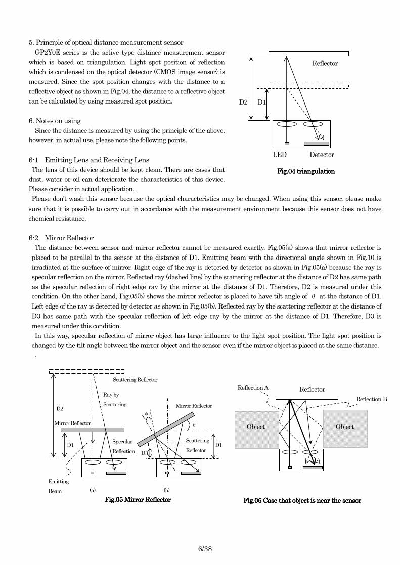
5. Principle of optical distance measurement sensor
GP2Y0E series is the active type distance measurement sensor
which is based on triangulation. Light spot position of reflection
which is condensed on the optical detector (CMOS image sensor) is
measured. Since the spot position changes with the distance to a
reflective object as shown in Fig.04, the distance to a reflective object
can be calculated by using measured spot position.
6. Notes on using
Since the distance is measured by using the principle of the above,
however, in actual use, please note the following points.
6-1 Emitting Lens and Receiving Lens
The lens of this device should be kept clean. There are cases that
dust, water or oil can deteriorate the characteristics of this device.
Please consider in actual application.
Please don’t wash this sensor because the optical characteristics may be changed. When using this sensor, please make
sure that it is possible to carry out in accordance with the measurement environment because this sensor does not have
chemical resistance.
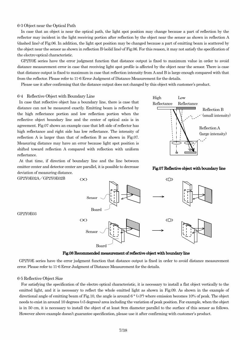
6-2 Mirror Reflector
The distance between sensor and mirror reflector cannot be measured exactly. Fig.05(a) shows that mirror reflector is
placed to be parallel to the sensor at the distance of D1. Emitting beam with the directional angle shown in Fig.10 is
irradiated at the surface of mirror. Right edge of the ray is detected by detector as shown in Fig.05(a) because the ray is
specular reflection on the mirror. Reflected ray (dashed line) by the scattering reflector at the distance of D2 has same path
as the specular reflection of right edge ray by the mirror at the distance of D1. Therefore, D2 is measured under this
condition. On the other hand, Fig.05(b) shows the mirror reflector is placed to have tilt angle of θ at the distance of D1.
Left edge of the ray is detected by detector as shown in Fig.05(b). Reflected ray by the scattering reflector at the distance of
D3 has same path with the specular reflection of left edge ray by the mirror at the distance of D1. Therefore, D3 is
measured under this condition.
In this way, specular reflection of mirror object has large influence to the light spot position. The light spot position is
changed by the tilt angle between the mirror object and the sensor even if the mirror object is placed at the same distance.
.
Fig.05 Mirror ReflectorFig.05 Mirror ReflectorFig.05 Mirror ReflectorFig.05 Mirror Reflector Fig.06 Case thFig.06 Case thFig.06 Case thFig.06 Case that object is near the sensorat object is near the sensorat object is near the sensorat object is near the sensor
Object Object
Reflector Reflection A
Reflection B
(a)
D1
D2
Scattering Reflector
Mirror Reflector
(b)
Ray by
Scattering
Specular
Reflection
Emitting
Beam
D1 D2
Detector LED
Reflector
FigFigFigFig.04 triangulation.04 triangulation.04 triangulation.04 triangulation
D1
θ
φ
Mirror Reflector
D3
Scattering
Reflector
7/38
6-3 Object near the Optical Path
In case that an object is near the optical path, the light spot position may change because a part of reflection by the
reflector may incident in the light receiving portion after reflection by the object near the sensor as shown in reflection A
(dashed line) of Fig.06. In addition, the light spot position may be changed because a part of emitting beam is scattered by
the object near the sensor as shown in reflection B (solid line) of Fig.06. For this reason, it may not satisfy the specification of
the electro-optical characteristic.
GP2Y0E series have the error judgment function that distance output is fixed to maximum value in order to avoid
distance measurement error in case that receiving light spot profile is affected by the object near the sensor. There is case
that distance output is fixed to maximum in case that reflection intensity from A and B is large enough compared with that
from the reflector. Please refer to 11-6 Error Judgment of Distance Measurement for the details.
Please use it after confirming that the distance output does not changed by this object with customer’s product.
6-4 Reflective Object with Boundary Line
In case that reflective object has a boundary line, there is case that
distance can not be measured exactly. Emitting beam is reflected by
the high reflectance portion and low reflection portion when the
reflective object boundary line and the center of optical axis is in
agreement. Fig.07 shows an example case that left side of reflector has
high reflectance and right side has low reflectance. The intensity of
reflection A is larger than that of reflection B as shown in Fig.07.
Measuring distance may have an error because light spot position is
shifted toward reflection A compared with reflection with uniform
reflectance.
At that time, if direction of boundary line and the line between
emitter center and detector center are parallel, it is possible to decrease
deviation of measuring distance.
GP2Y0E02A/GP2Y0E02B
GP2Y0E03
GP2Y0E series have the error judgment function that distance output is fixed in order to avoid distance measurement
error. Please refer to 11-6 Error Judgment of Distance Measurement for the details.
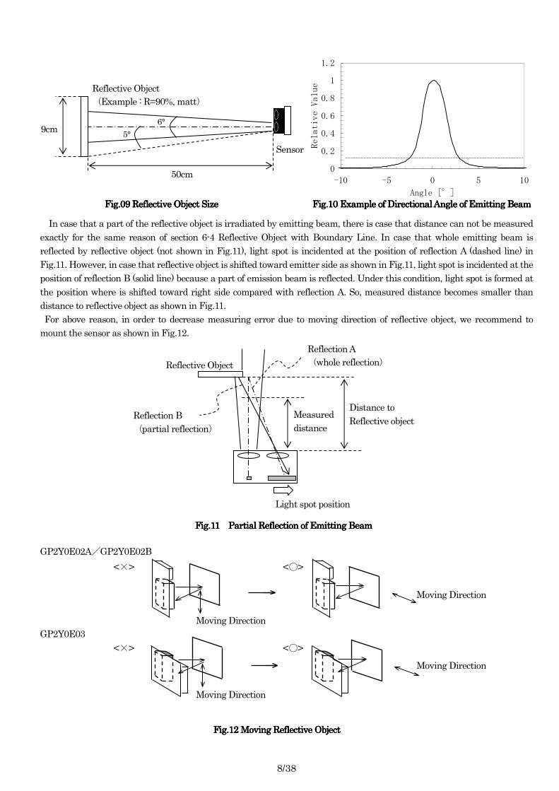
6-5 Reflective Object Size
For satisfying the specification of the electro optical characteristic, it is necessary to install a flat object vertically to the
emitted light, and it is necessary to reflect the whole emitted light as shown in Fig.09. As shown in the example of
directional angle of emitting beam of Fig.10, the angle is around 6 ° (±3°) where emission becomes 10% of peak. The object
needs to exist in around 10 degrees (±5 degrees) area including the variation of peak position. For example, when the object
is in 50 cm, it is necessary to install the object of at least 9cm diameter parallel to the surface of this sensor as follows.
However above example doesn’t guarantee specification, please use it after confirming with customer’s product.
Fig.08 ReFig.08 ReFig.08 ReFig.08 Recommendcommendcommendcommended measurement of reflective object with boundary lineed measurement of reflective object with boundary lineed measurement of reflective object with boundary lineed measurement of reflective object with boundary line
Fig.07 Reflective object with boundary lineFig.07 Reflective object with boundary lineFig.07 Reflective object with boundary lineFig.07 Reflective object with boundary line
Reflection B
(small intensity)
Reflection A
(large intensity)
High Low
Reflectance Reflectance
Sensor
Board
<<<<××××>>>> <<<<○○○○>>>>
<<<<××××>>>> <<<<○○○○>>>>
Sensor
Board
8/38
Light spot position
Distance to
Reflective object Measured
distance
Reflective Object
Reflection A
(whole reflection)
Reflection B
(partial reflection)
In case that a part of the reflective object is irradiated by emitting beam, there is case that distance can not be measured
exactly for the same reason of section 6-4 Reflective Object with Boundary Line. In case that whole emitting beam is
reflected by reflective object (not shown in Fig.11), light spot is incidented at the position of reflection A (dashed line) in
Fig.11. However, in case that reflective object is shifted toward emitter side as shown in Fig.11, light spot is incidented at the
position of reflection B (solid line) because a part of emission beam is reflected. Under this condition, light spot is formed at
the position where is shifted toward right side compared with reflection A. So, measured distance becomes smaller than
distance to reflective object as shown in Fig.11.
For above reason, in order to decrease measuring error due to moving direction of reflective object, we recommend to
mount the sensor as shown in Fig.12.
GP2Y0E02A/GP2Y0E02B
GP2Y0E03
0
0.2
0.4
0.6
0.8
1
1.2
-10 -5 0 5 10
Angle [°]
Relative V
alue
Sensor
50cm
9cm
Reflective Object
(Example : R=90%, matt)
6°
5°
Fig.09 Reflective Object SizeFig.09 Reflective Object SizeFig.09 Reflective Object SizeFig.09 Reflective Object Size Fig.10 Example of Directional Angle of Emitting BeamFig.10 Example of Directional Angle of Emitting BeamFig.10 Example of Directional Angle of Emitting BeamFig.10 Example of Directional Angle of Emitting Beam
Fig.11Fig.11Fig.11Fig.11 Partial Reflection of Emitting BeamPartial Reflection of Emitting BeamPartial Reflection of Emitting BeamPartial Reflection of Emitting Beam
Fig.12 Moving Reflective ObjectFig.12 Moving Reflective ObjectFig.12 Moving Reflective ObjectFig.12 Moving Reflective Object
Moving Direction
Moving Direction
<×> <○>
Moving Direction
Moving Direction
<×> <○>
9/38
GP2Y0E series have the error judgment function that distance output is fixed to be maximum (64cm) to avoid distance
measurement error. Please refer to 11-6 Error Judgment of Distance Measurement for the details.
6-6 Tilt of Reflective Object
For satisfying the specification of the electro optical characteristic, it is necessary to install a flat object vertically to the
emitted light, and it is necessary to reflect the whole emitted light as shown in Fig.09. There is the case that it is not
possible to measure distance exactly in case that reflective object is installed with tilt angle to the sensor. Fig.13 is shown in
the example case that reflective object is installed with the tilt angle to the sensor. Fig.13(a) is shown that reflective object is
installed with the tilt angle of θ to the axis which the light emitting and receiving lens are arranged. Fig.13(b) is shown in
the example case that reflective object is installed with the tilt angle of φ in the direction perpendicular to Fig.13(a). Fig.14
is shown in the example of tilt angle dependence in case that reflective object (R=90%, matt) is installed at the distance of
50cm from the sensor. The distance output changes in dependence of the tilt angle for θ direction. But the tilt angle
dependence of distance output for φ direction is small. This characteristic is reference data measured by the arbitrarily
extracted sample and not guaranteed. Please use it after confirming with customer’s product.
In case that tilt angle for θis large, there is the case that the light spot size is changed largely compared with
recommendation condition of Fig.09. GP2Y0E series have the error judgment function that distance output is fixed to be
maximum to avoid distance measurement error. Please refer to 11-6 Error Judgment of Distance Measurement for the
details.
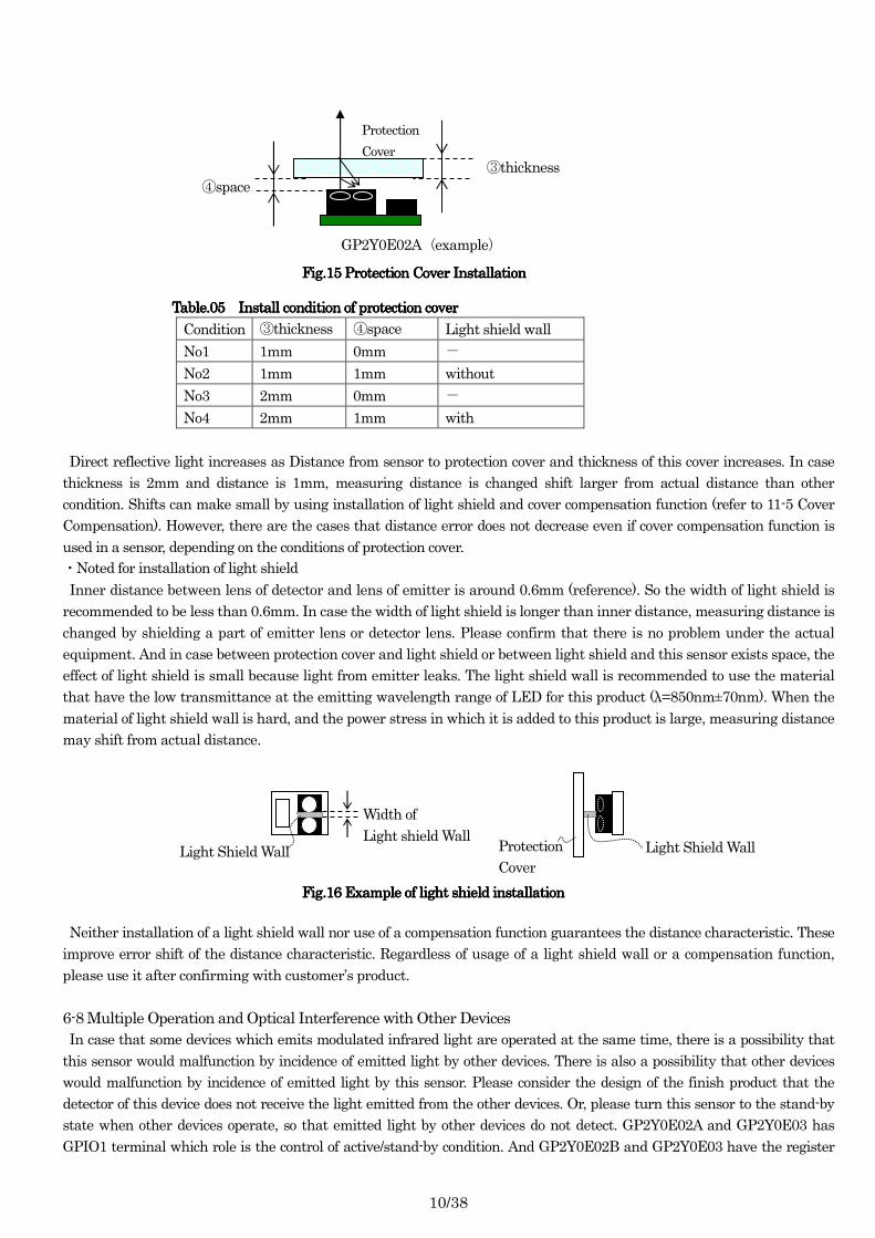
6-7 Protection Cover
In case that protection cover is set in front of this sensor, the protection cover shall be recommended to use material which
doesn’t scatter light and be matted finish. And the protection cover which has the most efficient transmittance at the
emitting wavelength range of LED for this product (λ=850nm±70nm). This protection cover is recommended to be flat. This
protection cover shall be recommended to be parallel to the emitter and detector portion. In case that protection cover is set
in front of this sensor, it emits reflected light from this protection cover. If this reflective light reaches in detector portion, the
output distance of this product may be changed. The output distance characteristics of this product may be changed with
according to material (①) or transmittance (②) or the thickness (③) or the distance between the protection cover and this
product (④) or the angle between surface and back (⑤) or the angle between this cover and this sensor (⑥). In case that
protection cover is set, please design to consider that this reflective light is minimized. It shall be effective to put light shield
wall between emitting lens and receiving lens as shown in Fig.16. Reference conditions in case of using protection cover are
shown in Table.05. Where, bellow are fixed condition that ①material=acrylic, ②transmittance>90%@850nm, ⑤angle
between surface and back of cover=parallel, ⑥angle between sensor and cover=parallel. In addition of above, surface and
back face of cover has mirror polished surface.
Fig.14 Tilt Angle Dependence of distance outputFig.14 Tilt Angle Dependence of distance outputFig.14 Tilt Angle Dependence of distance outputFig.14 Tilt Angle Dependence of distance output
40
45
50
55
60
-25 -20 -15 -10 -5 0 5 10 15 20 25
Tilt Angle[°]
Distance output(I2C)[cm]Object
+θ
Object
+φ
(a) (b)
Fig.13 RFig.13 RFig.13 RFig.13 Reflective Object with Tilt Angleeflective Object with Tilt Angleeflective Object with Tilt Angleeflective Object with Tilt Angle
Reflective Object
(R=90%, matt) @50cm ◆ tilt of θ
□ tilt of φ
10/38
Table.05 Table.05 Table.05 Table.05 Install condition of protection coverInstall condition of protection coverInstall condition of protection coverInstall condition of protection cover
Condition ③thickness ④space Light shield wall
No1 1mm 0mm -
No2 1mm 1mm without
No3 2mm 0mm -
No4 2mm 1mm with
Direct reflective light increases as Distance from sensor to protection cover and thickness of this cover increases. In case
thickness is 2mm and distance is 1mm, measuring distance is changed shift larger from actual distance than other
condition. Shifts can make small by using installation of light shield and cover compensation function (refer to 11-5 Cover
Compensation). However, there are the cases that distance error does not decrease even if cover compensation function is
used in a sensor, depending on the conditions of protection cover.
・Noted for installation of light shield
Inner distance between lens of detector and lens of emitter is around 0.6mm (reference). So the width of light shield is
recommended to be less than 0.6mm. In case the width of light shield is longer than inner distance, measuring distance is
changed by shielding a part of emitter lens or detector lens. Please confirm that there is no problem under the actual
equipment. And in case between protection cover and light shield or between light shield and this sensor exists space, the
effect of light shield is small because light from emitter leaks. The light shield wall is recommended to use the material
that have the low transmittance at the emitting wavelength range of LED for this product (λ=850nm±70nm). When the
material of light shield wall is hard, and the power stress in which it is added to this product is large, measuring distance
may shift from actual distance.
Neither installation of a light shield wall nor use of a compensation function guarantees the distance characteristic. These
improve error shift of the distance characteristic. Regardless of usage of a light shield wall or a compensation function,
please use it after confirming with customer’s product.
6-8 Multiple Operation and Optical Interference with Other Devices
In case that some devices which emits modulated infrared light are operated at the same time, there is a possibility that
this sensor would malfunction by incidence of emitted light by other devices. There is also a possibility that other devices
would malfunction by incidence of emitted light by this sensor. Please consider the design of the finish product that the
detector of this device does not receive the light emitted from the other devices. Or, please turn this sensor to the stand-by
state when other devices operate, so that emitted light by other devices do not detect. GP2Y0E02A and GP2Y0E03 has
GPIO1 terminal which role is the control of active/stand-by condition. And GP2Y0E02B and GP2Y0E03 have the register
Light Shield Wall Protection
Cover
Light Shield Wall
Width of
Light shield Wall
GP2Y0E02A(example)
Protection
Cover ③thickness
④space
Fig.15 Protection Cover Fig.15 Protection Cover Fig.15 Protection Cover Fig.15 Protection Cover InstallationInstallationInstallationInstallation
Fig.16 Example of light shield installatiFig.16 Example of light shield installatiFig.16 Example of light shield installatiFig.16 Example of light shield installationononon
11/38
for active /stand-by state control through I2C communication. When some these sensors are used for the same bus, slave
address of I2C can be changed to one of the 16 states by using of E-Fuse. So, it is possible to control some sensors via I2C
communication
7. Response Time
It is possible for this distance measuring sensor to detect the distance from 50cm to 4cm and the reflective object from high
reflectance to low reflectance. Detector of this sensor has the function (**) that signal intensity is automatically adjusted in
order to detect the reflection with wide dynamic range. Time to output the first distance value is changed by the condition of
reflective object because it takes time that this auto adjustment function operates, though this sensor outputs measured
distance value after first measurement. Response time defined in electro-optical characteristic of the specification sheet
means maximum time to operate auto adjustment function. Digital output (I2C bus) keeps maximum distance of output
(64cm) and analog output is 0V till first measurement is completed. It takes approx 2ms to stabilize Vout(A) because analog
output has built-in Low-Pass filter in the board. Response time of specification includes this stabilization time of analog
output.
If operating condition such as signal accumulation and median filter is changed, response time is not satisfied with one
defined in specification sheet. Please refer to 11-2 maximum pulse width of emitting and 11-3 signal accumulation for the
change of operating condition.
(**)The function that measurement is repeated while adjusting gain etc of signal processing circuit till signal intensity
becomes suitable level for distance calculation. After adjustment to become suitable level of signal intensity, distance
measurement starts. (Refer to Fig.22)
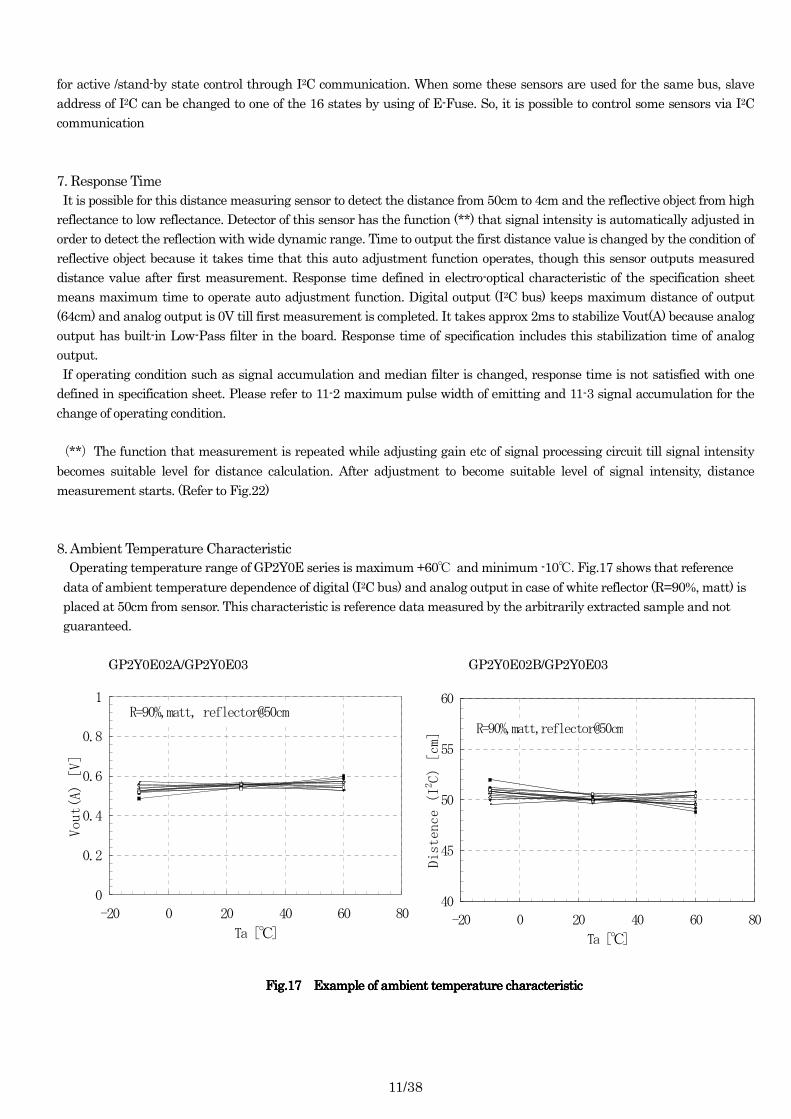
8. Ambient Temperature Characteristic
Operating temperature range of GP2Y0E series is maximum +60℃ and minimum -10℃. Fig.17 shows that reference
data of ambient temperature dependence of digital (I2C bus) and analog output in case of white reflector (R=90%, matt) is
placed at 50cm from sensor. This characteristic is reference data measured by the arbitrarily extracted sample and not
guaranteed.
GP2Y0E02A/GP2Y0E03 GP2Y0E02B/GP2Y0E03
40
45
50
55
60
-20 0 20 40 60 80
Ta [℃]
Distence(I2 C)[cm] R=90%,matt,reflector@50cm
0
0.2
0.4
0.6
0.8
1
-20 0 20 40 60 80
Ta [℃]
Vou
t(A)
[V]
R=90%,matt, reflector@50cm
Fig.17Fig.17Fig.17Fig.17 Example of ambient temperature characteristicExample of ambient temperature characteristicExample of ambient temperature characteristicExample of ambient temperature characteristic
12/38
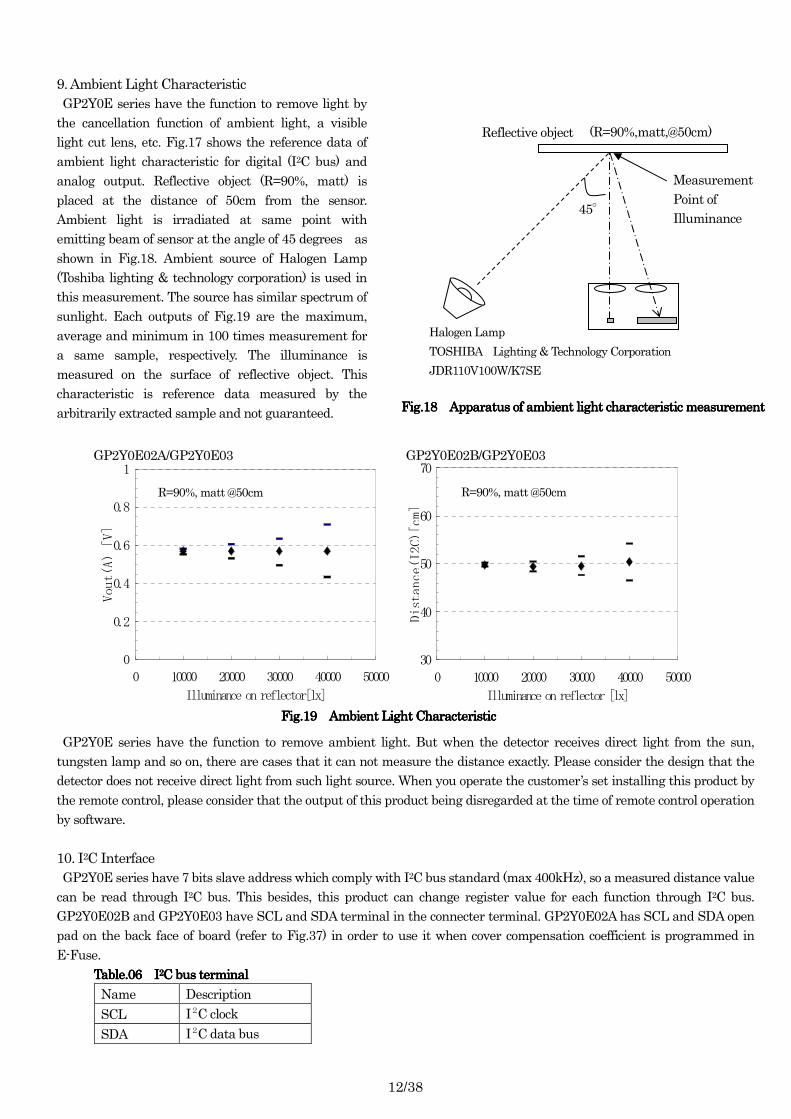
9. Ambient Light Characteristic
GP2Y0E series have the function to remove light by
the cancellation function of ambient light, a visible
light cut lens, etc. Fig.17 shows the reference data of
ambient light characteristic for digital (I2C bus) and
analog output. Reflective object (R=90%, matt) is
placed at the distance of 50cm from the sensor.
Ambient light is irradiated at same point with
emitting beam of sensor at the angle of 45 degrees as
shown in Fig.18. Ambient source of Halogen Lamp
(Toshiba lighting & technology corporation) is used in
this measurement. The source has similar spectrum of
sunlight. Each outputs of Fig.19 are the maximum,
average and minimum in 100 times measurement for
a same sample, respectively. The illuminance is
measured on the surface of reflective object. This
characteristic is reference data measured by the
arbitrarily extracted sample and not guaranteed.
GP2Y0E series have the function to remove ambient light. But when the detector receives direct light from the sun,
tungsten lamp and so on, there are cases that it can not measure the distance exactly. Please consider the design that the
detector does not receive direct light from such light source. When you operate the customer’s set installing this product by
the remote control, please consider that the output of this product being disregarded at the time of remote control operation
by software.
10. I2C Interface
GP2Y0E series have 7 bits slave address which comply with I2C bus standard (max 400kHz), so a measured distance value
can be read through I2C bus. This besides, this product can change register value for each function through I2C bus.
GP2Y0E02B and GP2Y0E03 have SCL and SDA terminal in the connecter terminal. GP2Y0E02A has SCL and SDA open
pad on the back face of board (refer to Fig.37) in order to use it when cover compensation coefficient is programmed in
E-Fuse.
Table.06Table.06Table.06Table.06 IIII2222CCCC bus terminalbus terminalbus terminalbus terminal
Name Description
SCL I2C clock
SDA I2C data bus
0
0.2
0.4
0.6
0.8
1
0 10000 20000 30000 40000 50000
Illuminance on reflector[lx]
Vout(A) [V]
R=90%, matt @50cm
GP2Y0E02A/GP2Y0E03
30
40
50
60
70
0 10000 20000 30000 40000 50000
Illuminance on reflector [lx]
Distance(I2C)[cm]
GP2Y0E02B/GP2Y0E03
R=90%, matt @50cm
Fig.Fig.Fig.Fig.11119999 Ambient Light CharacteristicAmbient Light CharacteristicAmbient Light CharacteristicAmbient Light Characteristic
Halogen Lamp
TOSHIBA Lighting & Technology Corporation
JDR110V100W/K7SE
45°
Reflective object (R=90%,matt,@50cm)
Measurement
Point of
Illuminance
Fig.18Fig.18Fig.18Fig.18 Apparatus of ambient light characteristic measurementApparatus of ambient light characteristic measurementApparatus of ambient light characteristic measurementApparatus of ambient light characteristic measurement
13/38
10-1 I2C data transfer format
Symbols explaining read and write format of GP2Y0E series are shown in the Table.07.
Table.07 Symbol of ITable.07 Symbol of ITable.07 Symbol of ITable.07 Symbol of I2222CCCC
Symbol Description Note
S Start Master output
A ACK Master/Slave output
NA NACK Master/Slave output
P Stop Master output
Address Register address Master output
Data Data Master/Slave output
10-2 Write format
1. Master generates start condition.
2. Master places 1st byte data that include slave address (7bit) with a read/write control bit.
3. Slave issues acknowledgment.
4. Master places 2nd byte address data on SDA.
5. Slave issues acknowledgment.
6. Master places 8 bits data on SDA.
7. Slave issues acknowledgement.
8. Master generates a stop condition to end this write cycle.
10-3 Read format
(1st cycle) (2nd cycle)
1st cycle
1. Master generates a start condition.
2. Master places 1st byte data that are combined slave address (7bits) with a read/write control bit (R/W=0) to SDA.
3. Slave issues acknowledgement.
4. Master places 2nd byte address data on SDA.
5. Slave issues acknowledgement.
6. Master generates a stop condition to end 1st cycle.
2nd cycle
7. Master generates a start condition.
8. Master places 1st byte data that are combined slave address (7bits) with a read/write control bit (R/W=1) to SDA.
9. Slave issues acknowledgement.
10. 8 bits data is read from internal control register of this product which address was assigned by 1st cycle.
11. Master generates negative acknowledgement.
12. Master generates a stop condition to end this read cycle.
Maste output
Slave output 0x80(default)
0x80(default) 0x81(default)
14/38
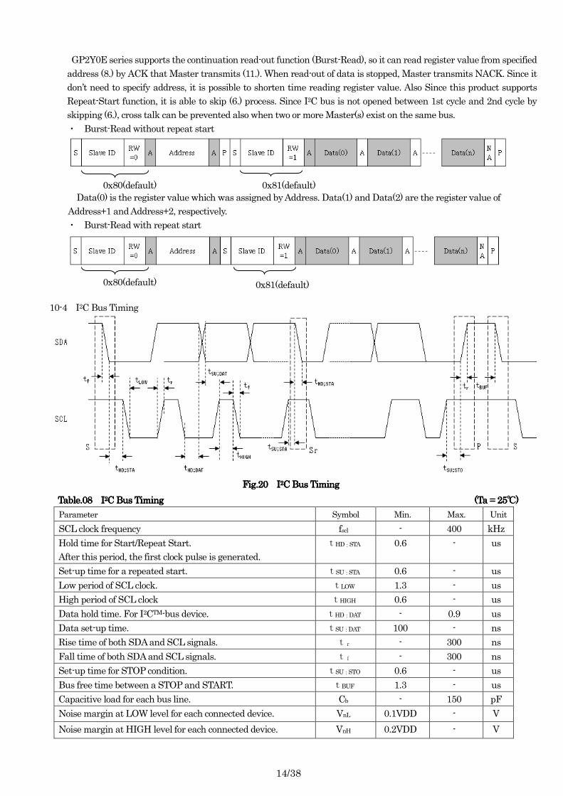
GP2Y0E series supports the continuation read-out function (Burst-Read), so it can read register value from specified
address (8.) by ACK that Master transmits (11.). When read-out of data is stopped, Master transmits NACK. Since it
don’t need to specify address, it is possible to shorten time reading register value. Also Since this product supports
Repeat-Start function, it is able to skip (6.) process. Since I2C bus is not opened between 1st cycle and 2nd cycle by
skipping (6.), cross talk can be prevented also when two or more Master(s) exist on the same bus.
・ Burst-Read without repeat start
Data(0) is the register value which was assigned by Address. Data(1) and Data(2) are the register value of
Address+1 and Address+2, respectively.
・ Burst-Read with repeat start
10-4 I2C Bus Timing
Table.08Table.08Table.08Table.08 IIII2222CCCC Bus TimingBus TimingBus TimingBus Timing (Ta = 25(Ta = 25(Ta = 25(Ta = 25℃℃℃℃))))
Parameter Symbol Min. Max. Unit
SCL clock frequency fscl - 400 kHz
Hold time for Start/Repeat Start.
After this period, the first clock pulse is generated.
tHD:STA 0.6 - us
Set-up time for a repeated start. tSU:STA 0.6 - us
Low period of SCL clock. tLOW 1.3 - us
High period of SCL clock tHIGH 0.6 - us
Data hold time. For I2CTM-bus device. tHD:DAT - 0.9 us
Data set-up time. tSU:DAT 100 - ns
Rise time of both SDA and SCL signals. tr - 300 ns
Fall time of both SDA and SCL signals. tf - 300 ns
Set-up time for STOP condition. tSU:STO 0.6 - us
Bus free time between a STOP and START. tBUF 1.3 - us
Capacitive load for each bus line. Cb - 150 pF
Noise margin at LOW level for each connected device. VnL 0.1VDD - V
Noise margin at HIGH level for each connected device. VnH 0.2VDD - V
0x80(default) 0x81(default)
0x80(default) 0x81(default)
Fig.20Fig.20Fig.20Fig.20 IIII2222C Bus TimingC Bus TimingC Bus TimingC Bus Timing
15/38
10-5 I2C DC Timing Characteristic
・GP2Y0E02A/GP2Y0E02B
Table.09 Table.09 Table.09 Table.09 IIII2222CCCC DC Timing CharacteristicDC Timing CharacteristicDC Timing CharacteristicDC Timing Characteristic 1111 (Ta = 25(Ta = 25(Ta = 25(Ta = 25℃℃℃℃))))
Parameter Symbol Standard Mode Fast Mode Unit
Min. Max. Min. Max.
Low level input voltage VIL -0.3 0.3VDD -0.3 0.3VDD V
High level input voltage VIH 0.7VDD VDD+0.3 0.7VDD VDD+0.3 V
Hysteresis of Schmitt trigger inputs Vhys - - 0.05VDD - V
Low level output voltage (open drain of open
collector) at 3mA sink current
VOL 0 0.4 0 0.4 V
Output fall time from VIHmin to VILmax
with a bus capacitance from 10pF to 400pF
TOF
- 250 - 250 ns
Pulse width of spikes which must be
suppressed by the input filter
tSP - - 0 50 ns
Input current each I/O pin with an input
voltage between 0.1VDD and 0.9VDDmax
II -10 10 -10 10 uA
・GP2Y0E03
Table.10 ITable.10 ITable.10 ITable.10 I2222C DC Timing CharacteristicC DC Timing CharacteristicC DC Timing CharacteristicC DC Timing Characteristic 2222 (Ta = 25(Ta = 25(Ta = 25(Ta = 25℃℃℃℃))))
Parameter Symbol Standard Mode Fast Mode Unit
Min. Max. Min. Max.
Low level input voltage VIL -0.3 0.3VIN(IO) -0.3 0.3VIN(IO) V
High level input voltage VIH 0.7VIN(IO) VIN(IO)+0.3
3.9
0.7VIN(IO) VIN(IO)+0.3
3.9
V
V
Hysteresis of Schmitt trigger inputs
VIN(IO) > 2V
VIN(IO) < 2V
Vhys
-
-
-
-
0.05VIN(IO)
0.1VIN(IO)
-
-
V
V
Low level output voltage (open drain of open
collector) at 3mA sink current
VIN(IO) > 2V
VIN(IO) < 2V
VOL
0
-
0.4
-
0
0
0.4
0.2VIN(IO)
V
V
Output fall time from VIHmin to VILmax
with a bus capacitance from 10pF to 400pF
TOF
- 250 - 250 ns
Pulse width of spikes which must be
suppressed by the input filter
tSP - - 0 50 ns
Input current each I/O pin with an input
voltage between 0.1VIN(IO) and
0.9VIN(IO)max
II -10 10 -10 10 uA
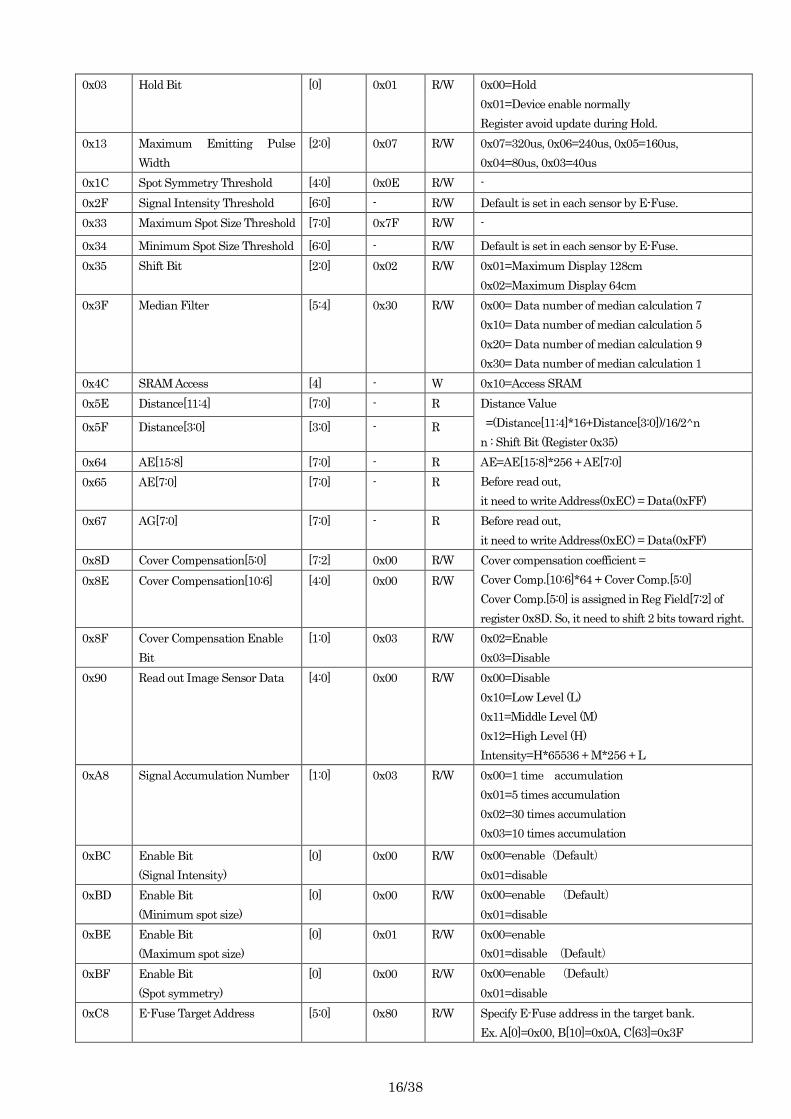
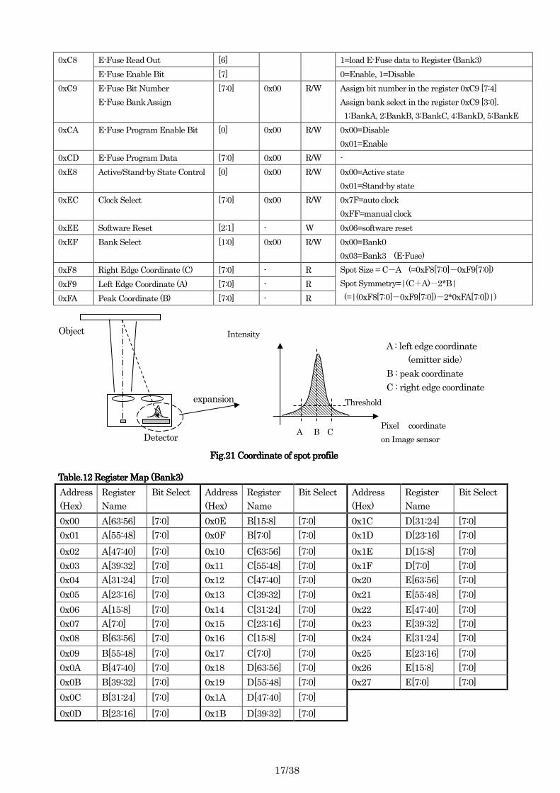
10-6 Register Map
Bank0 is register band for digital function control Bank3 is E-Fuse mapped register bank. Register 0xEF is used to
switch target register bank for register access. Setting 0x00 in the register 0xEF access to bank0, and setting 0x03 access
to bank3.
Table.11 Register Map (Bank0)
Address
(Hex)
Register Name Reg Field Default R/W Description
- Slave ID (write cycle) - 0x80 R -
- Slave ID (read cycle) - 0x81 R -
16/38
0x03 Hold Bit [0] 0x01 R/W 0x00=Hold
0x01=Device enable normally
Register avoid update during Hold.
0x13
Maximum Emitting Pulse
Width
[2:0]
0x07 R/W
0x07=320us, 0x06=240us, 0x05=160us,
0x04=80us, 0x03=40us
0x1C Spot Symmetry Threshold [4:0] 0x0E R/W -
0x2F Signal Intensity Threshold [6:0] - R/W Default is set in each sensor by E-Fuse.
0x33 Maximum Spot Size Threshold [7:0] 0x7F R/W -
0x34 Minimum Spot Size Threshold [6:0] - R/W Default is set in each sensor by E-Fuse.
0x35
Shift Bit
[2:0]
0x02
R/W
0x01=Maximum Display 128cm
0x02=Maximum Display 64cm
0x3F
Median Filter
[5:4]
0x30
R/W
0x00= Data number of median calculation 7
0x10= Data number of median calculation 5
0x20= Data number of median calculation 9
0x30= Data number of median calculation 1
0x4C SRAM Access [4] - W 0x10=Access SRAM
0x5E Distance[11:4] [7:0] - R Distance Value
=(Distance[11:4]*16+Distance[3:0])/16/2^n
n : Shift Bit (Register 0x35) 0x5F Distance[3:0] [3:0] - R
0x64 AE[15:8] [7:0] - R AE=AE[15:8]*256 + AE[7:0]
Before read out,
it need to write Address(0xEC) = Data(0xFF)
0x65 AE[7:0] [7:0] - R
0x67 AG[7:0] [7:0] - R Before read out,
it need to write Address(0xEC) = Data(0xFF)
0x8D Cover Compensation[5:0] [7:2] 0x00 R/W Cover compensation coefficient =
Cover Comp.[10:6]*64 + Cover Comp.[5:0]
Cover Comp.[5:0] is assigned in Reg Field[7:2] of
register 0x8D. So, it need to shift 2 bits toward right.
0x8E Cover Compensation[10:6] [4:0] 0x00 R/W
0x8F
Cover Compensation Enable
Bit
[1:0] 0x03 R/W 0x02=Enable
0x03=Disable
0x90 Read out Image Sensor Data [4:0] 0x00 R/W 0x00=Disable
0x10=Low Level (L)
0x11=Middle Level (M)
0x12=High Level (H)
Intensity=H*65536 + M*256 + L
0xA8
Signal Accumulation Number [1:0] 0x03 R/W 0x00=1 time accumulation
0x01=5 times accumulation
0x02=30 times accumulation
0x03=10 times accumulation
0xBC Enable Bit
(Signal Intensity)
[0] 0x00 R/W 0x00=enable(Default)
0x01=disable
0xBD Enable Bit
(Minimum spot size)
[0] 0x00 R/W 0x00=enable (Default)
0x01=disable
0xBE Enable Bit
(Maximum spot size)
[0] 0x01 R/W 0x00=enable
0x01=disable (Default)
0xBF Enable Bit
(Spot symmetry)
[0] 0x00 R/W 0x00=enable (Default)
0x01=disable
0xC8
E-Fuse Target Address
[5:0]
0x80 R/W Specify E-Fuse address in the target bank.
Ex. A[0]=0x00, B[10]=0x0A, C[63]=0x3F
17/38
0xC8 E-Fuse Read Out [6] 1=load E-Fuse data to Register (Bank3)
E-Fuse Enable Bit [7] 0=Enable, 1=Disable
0xC9 E-Fuse Bit Number
E-Fuse Bank Assign
[7:0] 0x00 R/W Assign bit number in the register 0xC9 [7:4]
Assign bank select in the register 0xC9 [3:0].
1:BankA, 2:BankB, 3:BankC, 4:BankD, 5:BankE
0xCA E-Fuse Program Enable Bit [0] 0x00 R/W 0x00=Disable
0x01=Enable
0xCD E-Fuse Program Data [7:0] 0x00 R/W -
0xE8
Active/Stand-by State Control [0] 0x00 R/W 0x00=Active state
0x01=Stand-by state
0xEC Clock Select [7:0] 0x00 R/W 0x7F=auto clock
0xFF=manual clock
0xEE Software Reset [2:1] - W 0x06=software reset
0xEF
Bank Select [1:0] 0x00 R/W 0x00=Bank0
0x03=Bank3 (E-Fuse)
0xF8 Right Edge Coordinate (C) [7:0] - R Spot Size = C-A (=0xF8[7:0]-0xF9[7:0])
Spot Symmetry=|(C+A)-2*B|
(=|(0xF8[7:0]-0xF9[7:0])-2*0xFA[7:0])|)
0xF9 Left Edge Coordinate (A) [7:0] - R
0xFA Peak Coordinate (B) [7:0] - R
Table.12 Register Map (Bank3)Table.12 Register Map (Bank3)Table.12 Register Map (Bank3)Table.12 Register Map (Bank3)
Address
(Hex)
Register
Name
Bit Select
Address
(Hex)
Register
Name
Bit Select
Address
(Hex)
Register
Name
Bit Select
0x00 A[63:56] [7:0] 0x0E B[15:8] [7:0] 0x1C D[31:24] [7:0]
0x01 A[55:48] [7:0] 0x0F B[7:0] [7:0] 0x1D D[23:16] [7:0]
0x02 A[47:40] [7:0] 0x10 C[63:56] [7:0] 0x1E D[15:8] [7:0]
0x03 A[39:32] [7:0] 0x11 C[55:48] [7:0] 0x1F D[7:0] [7:0]
0x04 A[31:24] [7:0] 0x12 C[47:40] [7:0] 0x20 E[63:56] [7:0]
0x05 A[23:16] [7:0] 0x13 C[39:32] [7:0] 0x21 E[55:48] [7:0]
0x06 A[15:8] [7:0] 0x14 C[31:24] [7:0] 0x22 E[47:40] [7:0]
0x07 A[7:0] [7:0] 0x15 C[23:16] [7:0] 0x23 E[39:32] [7:0]
0x08 B[63:56] [7:0] 0x16 C[15:8] [7:0] 0x24 E[31:24] [7:0]
0x09 B[55:48] [7:0] 0x17 C[7:0] [7:0] 0x25 E[23:16] [7:0]
0x0A B[47:40] [7:0] 0x18 D[63:56] [7:0] 0x26 E[15:8] [7:0]
0x0B B[39:32] [7:0] 0x19 D[55:48] [7:0] 0x27 E[7:0] [7:0]
0x0C B[31:24] [7:0] 0x1A D[47:40] [7:0]
0x0D B[23:16] [7:0] 0x1B D[39:32] [7:0]
Object
Detector
expansion
Pixel coordinate
on Image sensor
Intensity
A B C
A : left edge coordinate
(emitter side)
B : peak coordinate
C : right edge coordinate
Fig.21 Coordinate of spot profileFig.21 Coordinate of spot profileFig.21 Coordinate of spot profileFig.21 Coordinate of spot profile
Threshold

18/38
11. Functions which is possible to be set
GP2Y0E series has 7 bits slave address which complies with I2C bus standard (max400kHz), so various functions of this
product can be set by changing register value. Besides, GP2Y0E series has E-Fuse which is a nonvolatile OTP (One Time
Programmable Memory), so various functions of this product can be set by programming E-Fuse. In case power supply of
this sensor is OFF, this sensor keeps some programs that is written in E-Fuse. So when power supply is ON again, this
sensor operates under the programmed condition as before.
Table.13 shows the list of functions which can be set in GP2Y0E series.
Table.1Table.1Table.1Table.13 Functions which can be set by programming E3 Functions which can be set by programming E3 Functions which can be set by programming E3 Functions which can be set by programming E----FuseFuseFuseFuse and through Iand through Iand through Iand through I2222C busC busC busC bus
No. Description E-Fuse I2C Default (Recommand)
Value
Affected Characteristic
1 Slave Address ○ × Write : 0x80
Read : 0x81
-
2 Maximum Pulse Width
of Emitting
○ ○ 320us Operating Average Current
Stability of Distance Output
3 Signal Accumulation ○ ○ 10 Response Time
Stability of Distance Output
4 Median Filter ○ ○ 1 Response Time
Stability of Distance Output
5 Cover Compensation ○ ○ Disable Distance Characteristic
6-1 Error Judgment
(Signal Intensity)
Configured ○ Individual value Distance Characteristic
6-2 Error Judgment
(Minimum spot size)
Configured ○ Individual value Distance Characteristic
6-3 Error Judgment
(Maximum spot size)
○ ○ Disable Distance Characteristic
6-4 Error Judgment
(Spot Symmetry)
Configured ○ 14 Distance Characteristic
7 Maximum Output Distance Configured ○ 64cm Analog Output
8 Active/Stand-by State Control × ○ - -
9 Software Reset × ○ - -
11-1 Slave Address
GP2Y0E02B and GP2Y0E03 can be changed to 16 kinds of slave address in order to avoid overlap with other device
connecting with same bus, or when several this products are used connecting with same bus. Please refer to 12-4 (1) I2C
slave address with respect to the detail changing method..
Table.14 shows the list of slave address which can be changed.
Table.14 List of Slave AddresTable.14 List of Slave AddresTable.14 List of Slave AddresTable.14 List of Slave Address (s (s (s (GP2Y0E02BGP2Y0E02BGP2Y0E02BGP2Y0E02B、、、、GP2Y0E03GP2Y0E03GP2Y0E03GP2Y0E03))))
No Write CycleRead Cycle Note No Write CycleRead Cycle Note1 0x00 0x01 - 9 0x80 0x81 Default2 0x10 0x11 - 10 0x90 0x91 -3 0x20 0x21 - 11 0xA0 0xA1 -4 0x30 0x31 - 12 0xB0 0xB1 -5 0x40 0x41 - 13 0xC0 0xC1 -6 0x50 0x51 - 14 0xD0 0xD1 -7 0x60 0x61 - 15 0xE0 0xE1 -8 0x70 0x71 - 16 0xF0 0xF1 -

19/38
11-2 Maximum Pulse Width of Emitting
GP2Y0E series have the function which adjust emitting power by detecting signal intensity. Emitting power is
adjusted by control of emitting pulse width. Average current consumption decrease by restricting maximum emitting
pulse width. However, distance characteristic change, especially distance output may become unstable in case of
detecting reflector at far distance and with low reflectance because signal intensity is also decreased by restricting
maximum emitting pulse width. Response time does not change even if maximum emitting pulse width is decreased.
In case that maximum pulse width of emitting is changed, there is the case that electro optical characteristic described
in specification sheet becomes not to be satisfied. Please use it after confirming with customer’s product. Table.15
shows the relation between maximum pulse width of emitting (setting value) and operating average current
consumption. Please refer to the register 0x13 in register map (bank0) of table.11 with respect to the method of
bank0 register setting. And, please refer to 12-4(2) maximum pulse width of emitting with respect to programming
in E-Fuse.
Table.15 Maximum pulse width of emitting and operating averageTable.15 Maximum pulse width of emitting and operating averageTable.15 Maximum pulse width of emitting and operating averageTable.15 Maximum pulse width of emitting and operating average current consumptioncurrent consumptioncurrent consumptioncurrent consumption
No Max. pulse width of emitting
(setting value)
Average current consumption Note
1 320us Approx. 26mA Default
2 240us Approx. 22mA -
3 160us Approx. 18mA -
4 80us Approx. 14mA -
5 40us Approx. 12mA -
11-3 Signal Accumulation
GP2Y0E series calculate the light spot position after accumulation of several emitting pulse signals and calculate the
distance value. Response time can decrease by decreasing of signal accumulation times. However, distance
characteristic change, especially the distance output may become unstable in the case of detecting reflector at far
distance and the case with low reflectance, because signal intensity is decreased by decreasing signal accumulation
times. Response time does not change even if signal accumulation times are decreased. In case that signal
accumulation times are changed, there is the case that electro optical characteristic described in specification sheet
becomes not to be satisfied. Please use it after confirming with customer’s product. Please refer to the register 0xA8 in
register map (bank0) of table.11 with respect to the method of bank0 register setting. And, please refer to 12-4(3)
signal accumulation with respect to programming in E-Fuse.
Table.16 Signal accumulation times and response timeTable.16 Signal accumulation times and response timeTable.16 Signal accumulation times and response timeTable.16 Signal accumulation times and response time
No Signal Accumulation Times Response Time (Max) Measurement Period Note
1 1 20ms Approx. 1.9ms -
2 5 30ms Approx. 9.5ms -
3 10 40ms Approx. 19ms Default
4 30 80ms Approx. 57ms -
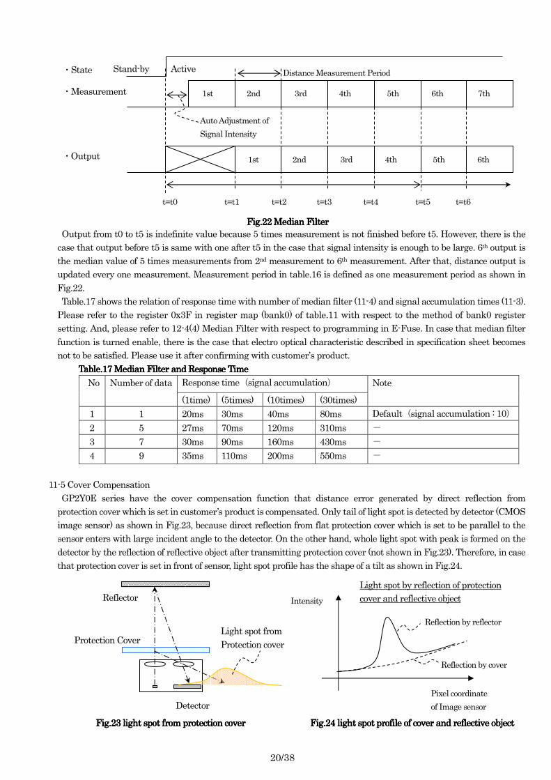
11-4 Median Filter
GP2Y0E series have the median calculation function by using several distance outputs in order to get stable output.
Response time increases though distance output becomes stable by using median calculation function. Median
calculation number can be selected to 5, 7 or 9. That is, in case of 5, a median of 5 distance values is output after 5 times
measurement. This sensor outputs measured distance after first measurement. However, output distance before
finishing the measurement times is not the result that median was calculated. Fig.22 shows the example that median
filter is set to 5.
20/38
Light spot from
Protection cover
Detector
Protection Cover
Reflector
Output from t0 to t5 is indefinite value because 5 times measurement is not finished before t5. However, there is the
case that output before t5 is same with one after t5 in the case that signal intensity is enough to be large. 6th output is
the median value of 5 times measurements from 2nd measurement to 6th measurement. After that, distance output is
updated every one measurement. Measurement period in table.16 is defined as one measurement period as shown in
Fig.22.
Table.17 shows the relation of response time with number of median filter (11-4) and signal accumulation times (11-3).
Please refer to the register 0x3F in register map (bank0) of table.11 with respect to the method of bank0 register
setting. And, please refer to 12-4(4) Median Filter with respect to programming in E-Fuse. In case that median filter
function is turned enable, there is the case that electro optical characteristic described in specification sheet becomes
not to be satisfied. Please use it after confirming with customer’s product.
Table.17 Median Filter and Response TimeTable.17 Median Filter and Response TimeTable.17 Median Filter and Response TimeTable.17 Median Filter and Response Time
No
Number of data Response time(signal accumulation) Note
(1time) (5times) (10times) (30times)
1 1 20ms 30ms 40ms 80ms Default(signal accumulation : 10)
2 5 27ms 70ms 120ms 310ms -
3 7 30ms 90ms 160ms 430ms -
4 9 35ms 110ms 200ms 550ms -
11-5 Cover Compensation
GP2Y0E series have the cover compensation function that distance error generated by direct reflection from
protection cover which is set in customer’s product is compensated. Only tail of light spot is detected by detector (CMOS
image sensor) as shown in Fig.23, because direct reflection from flat protection cover which is set to be parallel to the
sensor enters with large incident angle to the detector. On the other hand, whole light spot with peak is formed on the
detector by the reflection of reflective object after transmitting protection cover (not shown in Fig.23). Therefore, in case
that protection cover is set in front of sensor, light spot profile has the shape of a tilt as shown in Fig.24.
Stand-by Active
1st
Auto Adjustment of
Signal Intensity
・Output
・Measurement
・State
t=t0 t=t5
Fig.22 Median FilterFig.22 Median FilterFig.22 Median FilterFig.22 Median Filter
Fig.23 light spot from protection coverFig.23 light spot from protection coverFig.23 light spot from protection coverFig.23 light spot from protection cover Fig.2Fig.2Fig.2Fig.24444 light spot profile of cover and reflective objectlight spot profile of cover and reflective objectlight spot profile of cover and reflective objectlight spot profile of cover and reflective object
Pixel coordinate
of Image sensor
Intensity
Light spot by reflection of protection
cover and reflective object
Reflection by cover
Reflection by reflector
2nd 3rd 4th 5th 6th 7th
1st 2nd 3rd 4th 5th 6th
t=t1 t=t2 t=t3 t=t4 t=t6
Distance Measurement Period
21/38
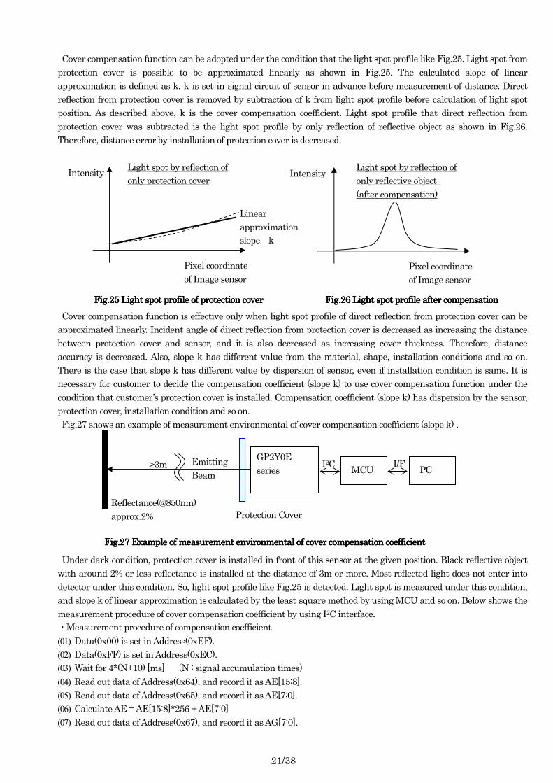
Cover compensation function can be adopted under the condition that the light spot profile like Fig.25. Light spot from
protection cover is possible to be approximated linearly as shown in Fig.25. The calculated slope of linear
approximation is defined as k. k is set in signal circuit of sensor in advance before measurement of distance. Direct
reflection from protection cover is removed by subtraction of k from light spot profile before calculation of light spot
position. As described above, k is the cover compensation coefficient. Light spot profile that direct reflection from
protection cover was subtracted is the light spot profile by only reflection of reflective object as shown in Fig.26.
Therefore, distance error by installation of protection cover is decreased.
Cover compensation function is effective only when light spot profile of direct reflection from protection cover can be
approximated linearly. Incident angle of direct reflection from protection cover is decreased as increasing the distance
between protection cover and sensor, and it is also decreased as increasing cover thickness. Therefore, distance
accuracy is decreased. Also, slope k has different value from the material, shape, installation conditions and so on.
There is the case that slope k has different value by dispersion of sensor, even if installation condition is same. It is
necessary for customer to decide the compensation coefficient (slope k) to use cover compensation function under the
condition that customer’s protection cover is installed. Compensation coefficient (slope k) has dispersion by the sensor,
protection cover, installation condition and so on.
Fig.27 shows an example of measurement environmental of cover compensation coefficient (slope k) .
Under dark condition, protection cover is installed in front of this sensor at the given position. Black reflective object
with around 2% or less reflectance is installed at the distance of 3m or more. Most reflected light does not enter into
detector under this condition. So, light spot profile like Fig.25 is detected. Light spot is measured under this condition,
and slope k of linear approximation is calculated by the least-square method by using MCU and so on. Below shows the
measurement procedure of cover compensation coefficient by using I2C interface.
・Measurement procedure of compensation coefficient
(01) Data(0x00) is set in Address(0xEF).
(02) Data(0xFF) is set in Address(0xEC).
(03) Wait for 4*(N+10) [ms] (N : signal accumulation times)
(04) Read out data of Address(0x64), and record it as AE[15:8].
(05) Read out data of Address(0x65), and record it as AE[7:0].
(06) Calculate AE = AE[15:8]*256 + AE[7:0]
(07) Read out data of Address(0x67), and record it as AG[7:0].
Pixel coordinate
of Image sensor
Intensity
Linear
approximation
slope=k
Light spot by reflection of
only protection cover
Pixel coordinate
of Image sensor
Intensity Light spot by reflection of
only reflective object
(after compensation)
GP2Y0E
series MCU PC
Protection Cover Reflectance(@850nm)
approx.2%
I2C I/F >3m Emitting
Beam
Fig.25 Light spot profile of protection coverFig.25 Light spot profile of protection coverFig.25 Light spot profile of protection coverFig.25 Light spot profile of protection cover Fig.26 Light spot profile after compensationFig.26 Light spot profile after compensationFig.26 Light spot profile after compensationFig.26 Light spot profile after compensation
Fig.2Fig.2Fig.2Fig.27777 Example of measurementExample of measurementExample of measurementExample of measurement environmental of cover compensation coefficientenvironmental of cover compensation coefficientenvironmental of cover compensation coefficientenvironmental of cover compensation coefficient
22/38
(08) Calculate 16
16]0:3[*2 16
]0:7[+
=AG
AG
AG
(09) Data(0x00) is set in Address(0x03).
(10) Wait for 2*(N+10) [ms]. (N : signal accumulation times)
(11) Data(0x10) is set in Address(0x4C).
(12) Wait for 2*(N+10) [ms]. (N : signal accumulation times)
(13) Data(0x10) is set in Address(0x90). (Read out setting of Low Level Data)
(14) Read out 220pcs of data with burst read from Address(0x00) to Address(0xDB), and record them as L[1:220].
Burst Read : refer to 10-3 Read Format
(15) Data(0x11) is set in Address(0x90). (Read out setting of Middle Level Data)
(16) Read out 220pcs of data with burst read from Address(0x00) to Address(0xDB), and record them as M[1:220].
(17) Data(0x12) is set in Address(0x90) (Read out setting of High Level Data)
(18) Read out 220pcs of data with burst read from Address(0x00) to Address(0xDB), and record them as H[1:220].
(19) Calculate ( )]220:1[256*]220:1[65536*]220:1[*295
*8
]220:1[ LMHAEAG
profile ++=
where, 1 and 220 of profile[1:220] shows X coordinate、Profile[1] shows Y coordinate of X=1.
Profile[1:220] shows the function of Y=profile[X]. (refer to Fig.28)
(20) Data(0x00) is set in Address(0x90).
(21) Data(0x01) is set in Address(0x03).
(22) Calculate k by using least-square method from Profile[1:220].
Material of protection cover : Acrylic(transmittance>90%@850nm)
Angle between surface and back face of protection cover : parallel
Angel between sensor and protection cover : parallel
Thickness of protection cover : 2mm
Distance between sensor and protection cover : 1mm
Reference value of slope k is around 350 under the above condition. This k value is reference data measured by the
arbitrarily extracted sample and not guaranteed. There is the case that it has large difference with the coefficient
measured under the customer’s condition. Please use it after confirming with customer’s product.
In case that k=350 is set in register (bank0), cover compensation [10:0] is separated into cover compensation [5:0] =
0b011110 and cover compensation [10:6] = 0b00101. Cover compensation [5:0] is available in register 0x8D of bank0
and cover compensation [10:6] is available in register 0x8E of bank0 as shown in register map(bank0) of Table.11.
Setting value in register 0x8E is 0x05 because cover compensation [10:6] is available in Reg Field [4:0]. However,
setting value in register 0x8D is 0x78 because cover compensation [5:0] is available in Reg Field [7:2]. That is,
0b011110 should be shifted left by 2 bits and 0b01111000 (=0x78) is calculated. Moreover, compensated distance
value is output after cover compensation function turns enable by setting data (0x02) in register 0x8F.
Please refer to 12-4(5) Cover Compensation with respect to the method of programming compensation coefficient in
E-Fuse.
1 220 X
profile[X] Linear approximation by least square method
(slope : k)
Fig.28 Read out light spot data Fig.28 Read out light spot data Fig.28 Read out light spot data Fig.28 Read out light spot data
23/38
11-6 Error Judgment of Distance Measurement
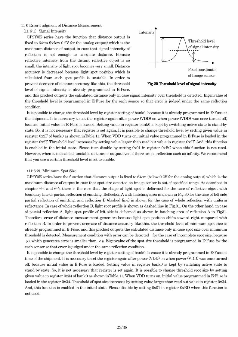
(11-6-1)Signal Intensity
GP2Y0E series have the function that distance output is
fixed to 64cm (below 0.2V for the analog output) which is the
maximum distance of output in case that signal intensity of
reflection is not enough to calculate distance. Because
reflective intensity from the distant reflective object is so
small, the intensity of light spot becomes very small. Distance
accuracy is decreased because light spot position which is
calculated from such spot profile is unstable. In order to
prevent decrease of distance accuracy like this, the threshold
level of signal intensity is already programmed in E-Fuse,
and this product outputs the calculated distance only in case signal intensity over threshold is detected. Eigenvalue of
the threshold level is programmed in E-Fuse for the each sensor so that error is judged under the same reflection
condition.
It is possible to change the threshold level by register setting of bank0, because it is already programmed in E-Fuse at
the shipment. It is necessary to set the register again after power (VDD) on when power (VDD) was once turned off,
because initial value in E-Fuse is loaded. Setting value in register bank0 is kept by switching active state to stand-by
state. So, it is not necessary that register is set again. It is possible to change threshold level by setting given value in
register 0x2F of bank0 as shown inTable.11. When VDD turns on, initial value programmed in E-Fuse is loaded in the
register 0x2F. Threshold level increases by setting value larger than read out value in register 0x2F. And, this function
is enabled in the initial state. Please turn disable by setting 0x01 in register 0xBC when this function is not used.
However, when it is disabled, unstable distance is output even if there are no reflection such as infinity. We recommend
that you use a certain threshold level is set to enable.
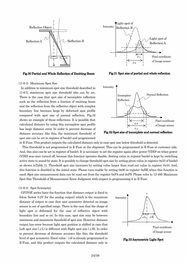
(11-6-2)Minimum Spot Size
GP2Y0E series have the function that distance output is fixed to 64cm (below 0.2V for the analog output) which is the
maximum distance of output in case that spot size detected on image sensor is out of specified range. As described in
chapter 6-4 and 6-5, there is the case that the shape of light spot is deformed for the case of reflective object with
boundary line or partial reflection of emitting. Reflection A with hatching area is shown in Fig.30 for the case of left side
partial reflection of emitting, and reflection B (dashed line) is shown for the case of whole reflection with uniform
reflectance. In case of whole reflection B, light spot profile is shown as dashed line in Fig.31. On the other hand, in case
of partial reflection A, light spot profile of left side is deformed as shown in hatching area of reflection A in Fig31.
Therefore, error of distance measurement generates because light spot position shifts toward right compared with
reflection B. In order to prevent decrease of distance accuracy like this, the threshold level of minimum spot size is
already programmed in E-Fuse, and this product outputs the calculated distance only in case spot size over minimum
threshold is detected. Measurement condition with error can be detected for the case of incomplete spot size, because
φA which generates error is smaller than φB. Eigenvalue of the spot size threshold is programmed in E-Fuse for the
each sensor so that error is judged under the same reflection condition.
It is possible to change the threshold level by register setting of bank0, because it is already programmed in E-Fuse at
time of the shipment. It is necessary to set the register again after power (VDD) on when power (VDD) was once turned
off, because initial value in E-Fuse is loaded. Setting value in register bank0 is kept by switching active state to
stand-by state. So, it is not necessary that register is set again. It is possible to change threshold spot size by setting
given value in register 0x34 of bank0 as shown inTable.11. When VDD turns on, initial value programmed in E-Fuse is
loaded in the register 0x34. Threshold of spot size increases by setting value larger than read out value in register 0x34.
And, this function is enabled in the initial state. Please disable by setting 0x01 in register 0xBD when this function is
not used.
Fig.29 Threshold level of signal intensityFig.29 Threshold level of signal intensityFig.29 Threshold level of signal intensityFig.29 Threshold level of signal intensity
Intensity
Pixel coordinate
of Image sensor
Threshold level
of signal intensity
24/38
(11-6-3)Maximum Spot Size
In addition to minimum spot size threshold described in
11-6-2, maximum spot size threshold also can be set.
There is the case that spot size of incomplete reflection
such as the reflection from a fraction of emitting beam
and the reflection from the reflective object with complex
boundary line becomes large by deformed spot profile
compared with spot size of normal reflection. Fig.32
shows an example of these reflections. It is possible that
calculated distance by using this incomplete spot profile
has large distance error. In order to prevent decrease of
distance accuracy like this, the maximum threshold of
spot size can be set in register of bank0 and programmed
in E-Fuse. This product outputs the calculated distance only in case spot size below threshold is detected.
This threshold is not programmed in E-Fuse at the shipment. This can be programmed in E-Fuse at customer side.
And, this also can be set in register of bank0. It is necessary to set the register again after power (VDD) on when power
(VDD) was once turned off, because this function operates disable. Setting value in register bank0 is kept by switching
active state to stand-by state. It is possible to change threshold spot size by setting given value in register 0x33 of bank0
as shown inTable.11. Threshold spot size increases by setting value larger than read out value in register 0x33. And,
this function is disabled in the initial state. Please turn enable by setting 0x00 in register 0xBE when this function is
used. Spot size measurement data can be read out from the register 0xF8 and 0xF9. Please refer to 12-4(6) Maximum
Spot Size Threshold of Measurement Error Judgment with respect to programming it in E-Fuse.
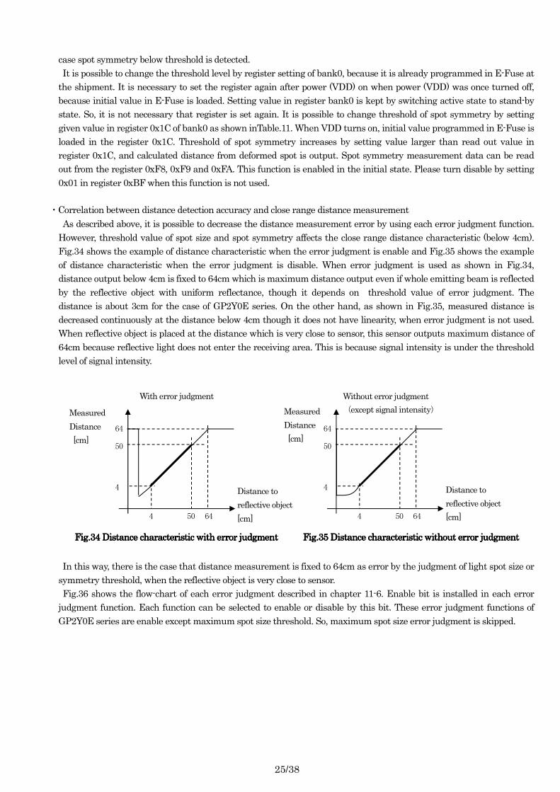
(11-6-4)Spot Symmetry
GP2Y0E series have the function that distance output is fixed to
64cm (below 0.2V for the analog output) which is the maximum
distance of output in case that spot symmetry detected on image
sensor is out of specified range. There is the case that the shape of
light spot is deformed for the case of reflective object with
boundary line and so on. In this case, spot size may be between
minimum and maximum threshold of spot size. However, distance
output has error because light spot position is shifted in case that
Left spot size (φL) is different with Right spot size (φR). In order
to prevent decrease of distance accuracy like this, the threshold
level of spot symmetry (fixed value : 14) is already programmed in
E-Fuse, and this product outputs the calculated distance only in
Fig.30 Partial and Whole Reflection of Emitting BeamFig.30 Partial and Whole Reflection of Emitting BeamFig.30 Partial and Whole Reflection of Emitting BeamFig.30 Partial and Whole Reflection of Emitting Beam Fig.31 Spot size of partial and whole reflectionFig.31 Spot size of partial and whole reflectionFig.31 Spot size of partial and whole reflectionFig.31 Spot size of partial and whole reflection
Fig.32 Spot size of incomplete and normal reflectionFig.32 Spot size of incomplete and normal reflectionFig.32 Spot size of incomplete and normal reflectionFig.32 Spot size of incomplete and normal reflection
Pixel coordinate
of Image sensor
Intensity
Normal Reflection Incomplete
Reflection
φA
φB
Pixel coordinate
of Image sensor
Intensity
Fig.33 Asymmetric Light SpotFig.33 Asymmetric Light SpotFig.33 Asymmetric Light SpotFig.33 Asymmetric Light Spot
φL φR
Reflection A Reflection B
Reflective Object
Pixel coordinate
of Image sensor
Intensity
Light spot of
Reflection A
Light spot of
Reflection B
φA
φB
25/38
case spot symmetry below threshold is detected.
It is possible to change the threshold level by register setting of bank0, because it is already programmed in E-Fuse at
the shipment. It is necessary to set the register again after power (VDD) on when power (VDD) was once turned off,
because initial value in E-Fuse is loaded. Setting value in register bank0 is kept by switching active state to stand-by
state. So, it is not necessary that register is set again. It is possible to change threshold of spot symmetry by setting
given value in register 0x1C of bank0 as shown inTable.11. When VDD turns on, initial value programmed in E-Fuse is
loaded in the register 0x1C. Threshold of spot symmetry increases by setting value larger than read out value in
register 0x1C, and calculated distance from deformed spot is output. Spot symmetry measurement data can be read
out from the register 0xF8, 0xF9 and 0xFA. This function is enabled in the initial state. Please turn disable by setting
0x01 in register 0xBF when this function is not used.
・Correlation between distance detection accuracy and close range distance measurement
As described above, it is possible to decrease the distance measurement error by using each error judgment function.
However, threshold value of spot size and spot symmetry affects the close range distance characteristic (below 4cm).
Fig.34 shows the example of distance characteristic when the error judgment is enable and Fig.35 shows the example
of distance characteristic when the error judgment is disable. When error judgment is used as shown in Fig.34,
distance output below 4cm is fixed to 64cm which is maximum distance output even if whole emitting beam is reflected
by the reflective object with uniform reflectance, though it depends on threshold value of error judgment. The
distance is about 3cm for the case of GP2Y0E series. On the other hand, as shown in Fig.35, measured distance is
decreased continuously at the distance below 4cm though it does not have linearity, when error judgment is not used.
When reflective object is placed at the distance which is very close to sensor, this sensor outputs maximum distance of
64cm because reflective light does not enter the receiving area. This is because signal intensity is under the threshold
level of signal intensity.
In this way, there is the case that distance measurement is fixed to 64cm as error by the judgment of light spot size or
symmetry threshold, when the reflective object is very close to sensor.
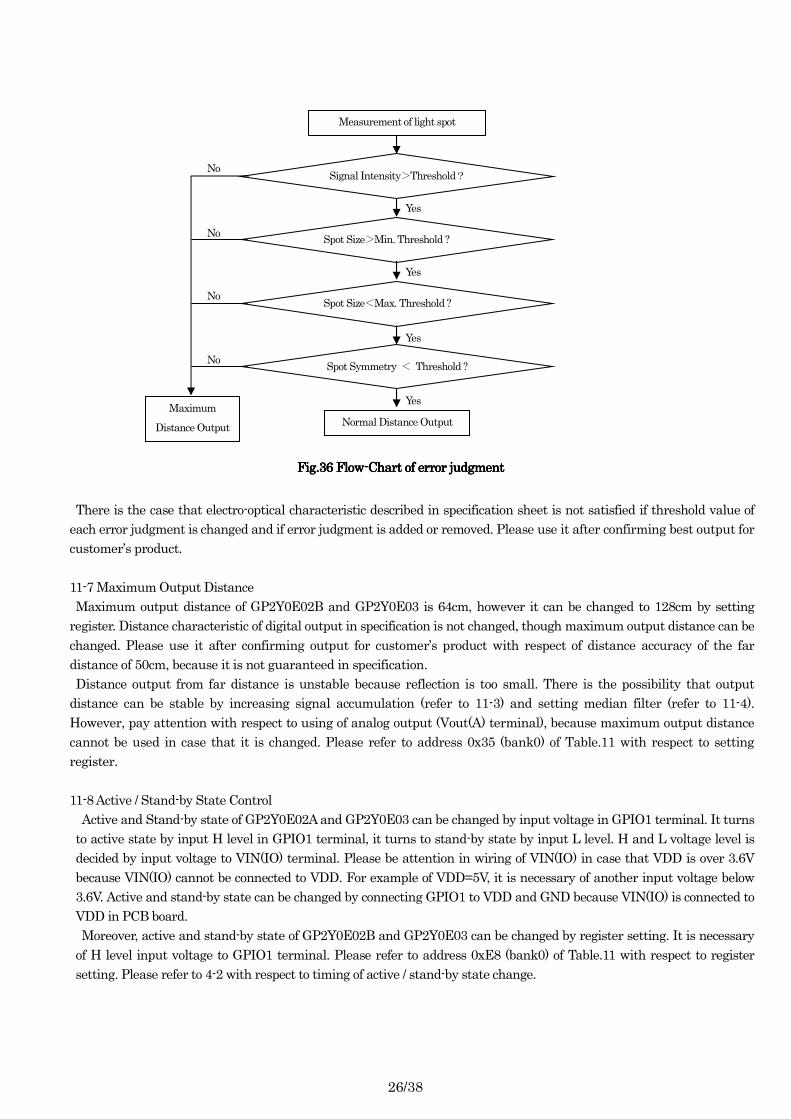
Fig.36 shows the flow-chart of each error judgment described in chapter 11-6. Enable bit is installed in each error
judgment function. Each function can be selected to enable or disable by this bit. These error judgment functions of
GP2Y0E series are enable except maximum spot size threshold. So, maximum spot size error judgment is skipped.
Distance to
reflective object
[cm]
Fig.34 Distance characteristic with error judgmentFig.34 Distance characteristic with error judgmentFig.34 Distance characteristic with error judgmentFig.34 Distance characteristic with error judgment
Distance to
reflective object
[cm]
Measured
Distance
[cm]
4 50
4
50
64
64
Measured
Distance
[cm]
4 50
4
50
64
64
With error judgment Without error judgment
(except signal intensity)
Fig.35 Distance characteristic without error judgmentFig.35 Distance characteristic without error judgmentFig.35 Distance characteristic without error judgmentFig.35 Distance characteristic without error judgment
26/38
There is the case that electro-optical characteristic described in specification sheet is not satisfied if threshold value of
each error judgment is changed and if error judgment is added or removed. Please use it after confirming best output for
customer’s product.
11-7 Maximum Output Distance
Maximum output distance of GP2Y0E02B and GP2Y0E03 is 64cm, however it can be changed to 128cm by setting
register. Distance characteristic of digital output in specification is not changed, though maximum output distance can be
changed. Please use it after confirming output for customer’s product with respect of distance accuracy of the far
distance of 50cm, because it is not guaranteed in specification.
Distance output from far distance is unstable because reflection is too small. There is the possibility that output
distance can be stable by increasing signal accumulation (refer to 11-3) and setting median filter (refer to 11-4).
However, pay attention with respect to using of analog output (Vout(A) terminal), because maximum output distance
cannot be used in case that it is changed. Please refer to address 0x35 (bank0) of Table.11 with respect to setting
register.
11-8 Active / Stand-by State Control
Active and Stand-by state of GP2Y0E02A and GP2Y0E03 can be changed by input voltage in GPIO1 terminal. It turns
to active state by input H level in GPIO1 terminal, it turns to stand-by state by input L level. H and L voltage level is
decided by input voltage to VIN(IO) terminal. Please be attention in wiring of VIN(IO) in case that VDD is over 3.6V
because VIN(IO) cannot be connected to VDD. For example of VDD=5V, it is necessary of another input voltage below
3.6V. Active and stand-by state can be changed by connecting GPIO1 to VDD and GND because VIN(IO) is connected to
VDD in PCB board.
Moreover, active and stand-by state of GP2Y0E02B and GP2Y0E03 can be changed by register setting. It is necessary
of H level input voltage to GPIO1 terminal. Please refer to address 0xE8 (bank0) of Table.11 with respect to register
setting. Please refer to 4-2 with respect to timing of active / stand-by state change.
Measurement of light spot
Signal Intensity>Threshold?
Spot Size>Min. Threshold ?
Spot Size<Max. Threshold ?
Spot Symmetry < Threshold ?
Normal Distance Output Maximum
Distance Output
Yes
Yes
Yes
Yes
No
No
No
No
Fig.36 FlowFig.36 FlowFig.36 FlowFig.36 Flow----Chart of error judgmentChart of error judgmentChart of error judgmentChart of error judgment
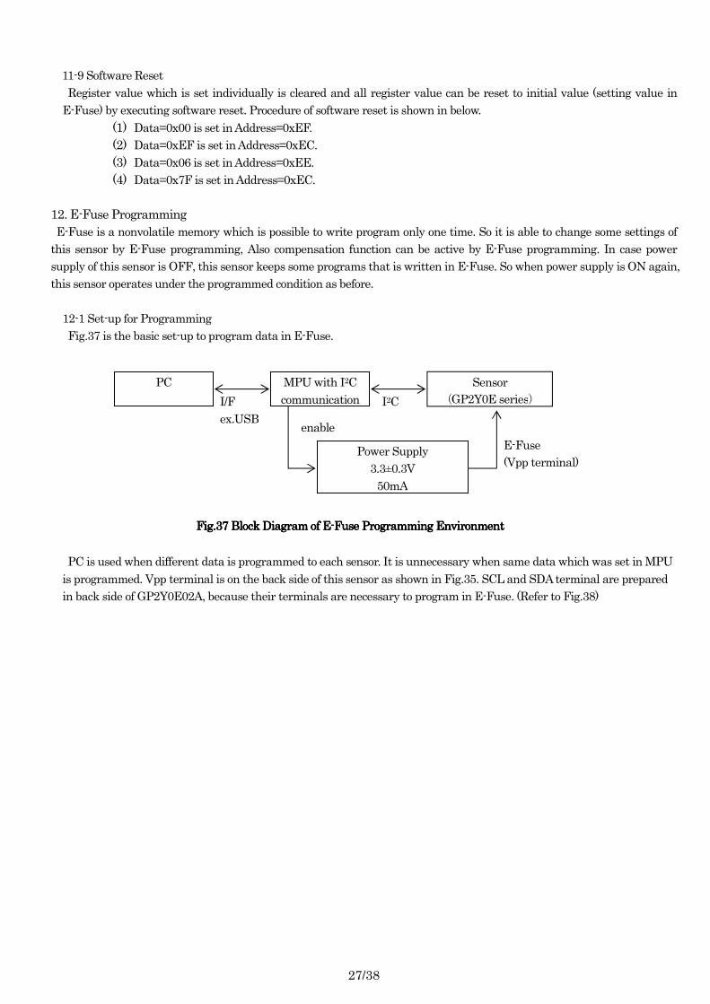
27/38
11-9 Software Reset
Register value which is set individually is cleared and all register value can be reset to initial value (setting value in
E-Fuse) by executing software reset. Procedure of software reset is shown in below.
(1) Data=0x00 is set in Address=0xEF.
(2) Data=0xEF is set in Address=0xEC.
(3) Data=0x06 is set in Address=0xEE.
(4) Data=0x7F is set in Address=0xEC.
12. E-Fuse Programming
E-Fuse is a nonvolatile memory which is possible to write program only one time. So it is able to change some settings of
this sensor by E-Fuse programming, Also compensation function can be active by E-Fuse programming. In case power
supply of this sensor is OFF, this sensor keeps some programs that is written in E-Fuse. So when power supply is ON again,
this sensor operates under the programmed condition as before.
12-1 Set-up for Programming
Fig.37 is the basic set-up to program data in E-Fuse.
PC is used when different data is programmed to each sensor. It is unnecessary when same data which was set in MPU
is programmed. Vpp terminal is on the back side of this sensor as shown in Fig.35. SCL and SDA terminal are prepared
in back side of GP2Y0E02A, because their terminals are necessary to program in E-Fuse. (Refer to Fig.38)
PC MPU with I2C
communication
Sensor
(GP2Y0E series)
Power Supply
3.3±0.3V
50mA
E-Fuse
(Vpp terminal)
enable
I/F
ex.USB
I2C
Fig.37 Block Diagram of EFig.37 Block Diagram of EFig.37 Block Diagram of EFig.37 Block Diagram of E----Fuse Programming EnvironmentFuse Programming EnvironmentFuse Programming EnvironmentFuse Programming Environment
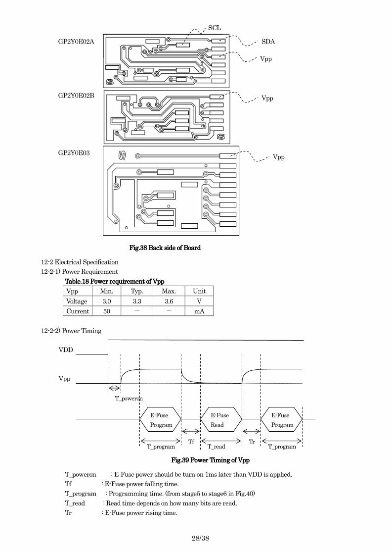
28/38
12-2 Electrical Specification
12-2-1) Power Requirement
Table.18 Power requirement of VppTable.18 Power requirement of VppTable.18 Power requirement of VppTable.18 Power requirement of Vpp
Vpp Min. Typ. Max. Unit
Voltage 3.0 3.3 3.6 V
Current 50 - - mA
12-2-2) Power Timing
VDD
Vpp
T_poweron : E-Fuse power should be turn on 1ms later than VDD is applied.
Tf : E-Fuse power falling time.
T_program : Programming time. (from stage5 to stage6 in Fig.40)
T_read : Read time depends on how many bits are read.
Tr : E-Fuse power rising time.
Vpp
T_poweron
E-Fuse
Program
E-Fuse
Read
E-Fuse
Program
Tf Tr T_program T_read T_program
Vpp
SDA GP2Y0E02A
GP2Y0E02B
GP2Y0E03
Vpp
SCL
Fig.38 Back side of BoardFig.38 Back side of BoardFig.38 Back side of BoardFig.38 Back side of Board
Fig.39 Power Timing of VppFig.39 Power Timing of VppFig.39 Power Timing of VppFig.39 Power Timing of Vpp
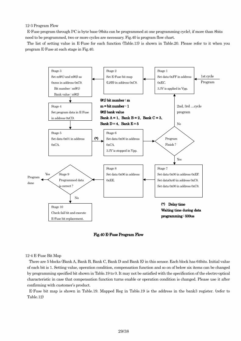
29/38
12-3 Program Flow
E-Fuse program through I2C is byte base (8bits can be programmed at one programming cycle), if more than 8bits
need to be programmed, two or more cycles are necessary. Fig.40 is program flow chart.
The list of setting value in E-Fuse for each function (Table.13) is shown in Table.20. Please refer to it when you
program E-Fuse at each stage in Fig.40.
12-4 E-Fuse Bit Map
There are 5 blocks (Bank A, Bank B, Bank C, Bank D and Bank E) in this sensor. Each block has 64bits. Initial value
of each bit is 1. Setting value, operation condition, compensation function and so on of below six items can be changed
by programming specified bit shown in Table.19 to 0. It may not be satisfied with the specification of the electro-optical
characteristic in case that compensation function turns enable or operation condition is changed. Please use it after
confirming with customer’s product.
E-Fuse bit map is shown in Table.19. Mapped Reg in Table.19 is the address in the bank3 register. (refer to
Table.12)
Stage 1
Set data 0xFF in address
0xEC.
3.3V is applied in Vpp.
1st cycle
Program
Stage 2
Set E-Fuse bit map
(LSB) in address 0xC8.
Stage 3
Set m(#1) and n(#2) as
0xmn in address 0xC9.
Bit number : m(#1)
Bank value : n(#2)
Stage 4
Set program data in E-Fuse
in address 0xCD.
Stage 5
Set data 0x01 in address
0xCA.
Stage 6
Set data 0x00 in address
0xCA.
3.3V is stopped in Vpp.
Program
Finish ?
2nd, 3rd …cycle
program
No
(*)(*)(*)(*)
Stage 7
Set data 0x00 in address 0xEF.
Set data0x40 in address 0xC8.
Set data 0x00 in address 0xC8.
Stage 8
Set data 0x06 in address
0xEE.
Stage 9
Programmed data
is correct ?
Yes
Program
done
Yes
No
Stage 10
Check fail bit and execute
E-Fuse bit replacement.
(*)(*)(*)(*) Delay timeDelay timeDelay timeDelay time
Waiting time during data Waiting time during data Waiting time during data Waiting time during data
programming : 500usprogramming : 500usprogramming : 500usprogramming : 500us
(#1)(#1)(#1)(#1) bit number : mbit number : mbit number : mbit number : m
mmmm ==== bit number bit number bit number bit number ---- 1111
(#2)(#2)(#2)(#2) bank valuebank valuebank valuebank value
Bank A = 1Bank A = 1Bank A = 1Bank A = 1、、、、Bank B = 2Bank B = 2Bank B = 2Bank B = 2、、、、Bank C = 3Bank C = 3Bank C = 3Bank C = 3、、、、
Bank D = 4Bank D = 4Bank D = 4Bank D = 4、、、、Bank E = 5Bank E = 5Bank E = 5Bank E = 5
Fig.40 EFig.40 EFig.40 EFig.40 E----Fuse Program FlowFuse Program FlowFuse Program FlowFuse Program Flow
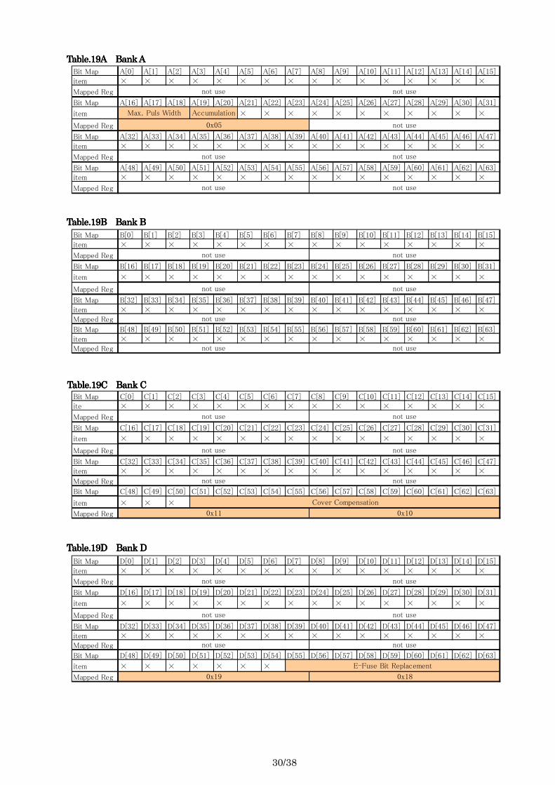
30/38
Table.Table.Table.Table.19A19A19A19A Bank ABank ABank ABank A
Table.Table.Table.Table.19B19B19B19B Bank BBank BBank BBank B
Table.Table.Table.Table.19C19C19C19C Bank CBank CBank CBank C
Table.Table.Table.Table.19D19D19D19D Bank DBank DBank DBank D
Bit Map A[0] A[1] A[2] A[3] A[4] A[5] A[6] A[7] A[8] A[9] A[10] A[11] A[12] A[13] A[14] A[15]
item × × × × × × × × × × × × × × × ×
Mapped Reg
Bit Map A[16] A[17] A[18] A[19] A[20] A[21] A[22] A[23] A[24] A[25] A[26] A[27] A[28] A[29] A[30] A[31]
item × × × × × × × × × × ×
Mapped Reg
Bit Map A[32] A[33] A[34] A[35] A[36] A[37] A[38] A[39] A[40] A[41] A[42] A[43] A[44] A[45] A[46] A[47]
item × × × × × × × × × × × × × × × ×
Mapped Reg
Bit Map A[48] A[49] A[50] A[51] A[52] A[53] A[54] A[55] A[56] A[57] A[58] A[59] A[60] A[61] A[62] A[63]
item × × × × × × × × × × × × × × × ×
Mapped Reg not use not use
not use
not use
not use not use
Max. Puls Width Accumulation
0x05
not use
Bit Map B[0] B[1] B[2] B[3] B[4] B[5] B[6] B[7] B[8] B[9] B[10] B[11] B[12] B[13] B[14] B[15]
item × × × × × × × × × × × × × × × ×
Mapped Reg
Bit Map B[16] B[17] B[18] B[19] B[20] B[21] B[22] B[23] B[24] B[25] B[26] B[27] B[28] B[29] B[30] B[31]
item × × × × × × × × × × × × × × × ×
Mapped Reg
Bit Map B[32] B[33] B[34] B[35] B[36] B[37] B[38] B[39] B[40] B[41] B[42] B[43] B[44] B[45] B[46] B[47]
item × × × × × × × × × × × × × × × ×Mapped Reg
Bit Map B[48] B[49] B[50] B[51] B[52] B[53] B[54] B[55] B[56] B[57] B[58] B[59] B[60] B[61] B[62] B[63]
item × × × × × × × × × × × × × × × ×Mapped Reg
not use not use
not use not use
not use not use
not use not use
Bit Map C[0] C[1] C[2] C[3] C[4] C[5] C[6] C[7] C[8] C[9] C[10] C[11] C[12] C[13] C[14] C[15]
ite × × × × × × × × × × × × × × × ×
Mapped Reg
Bit Map C[16] C[17] C[18] C[19] C[20] C[21] C[22] C[23] C[24] C[25] C[26] C[27] C[28] C[29] C[30] C[31]
item × × × × × × × × × × × × × × × ×
Mapped Reg
Bit Map C[32] C[33] C[34] C[35] C[36] C[37] C[38] C[39] C[40] C[41] C[42] C[43] C[44] C[45] C[46] C[47]
item × × × × × × × × × × × × × × × ×
Mapped Reg
Bit Map C[48] C[49] C[50] C[51] C[52] C[53] C[54] C[55] C[56] C[57] C[58] C[59] C[60] C[61] C[62] C[63]
item × × ×
Mapped Reg 0x11 0x10
Cover Compensation
not use not use
not use not use
not use not use
Bit Map D[0] D[1] D[2] D[3] D[4] D[5] D[6] D[7] D[8] D[9] D[10] D[11] D[12] D[13] D[14] D[15]
item × × × × × × × × × × × × × × × ×
Mapped Reg
Bit Map D[16] D[17] D[18] D[19] D[20] D[21] D[22] D[23] D[24] D[25] D[26] D[27] D[28] D[29] D[30] D[31]
item × × × × × × × × × × × × × × × ×
Mapped Reg
Bit Map D[32] D[33] D[34] D[35] D[36] D[37] D[38] D[39] D[40] D[41] D[42] D[43] D[44] D[45] D[46] D[47]
item × × × × × × × × × × × × × × × ×
Mapped Reg
Bit Map D[48] D[49] D[50] D[51] D[52] D[53] D[54] D[55] D[56] D[57] D[58] D[59] D[60] D[61] D[62] D[63]
item × × × × × × ×
Mapped Reg 0x19 0x18
E-Fuse Bit Replacement
not use not use
not use not use
not use not use
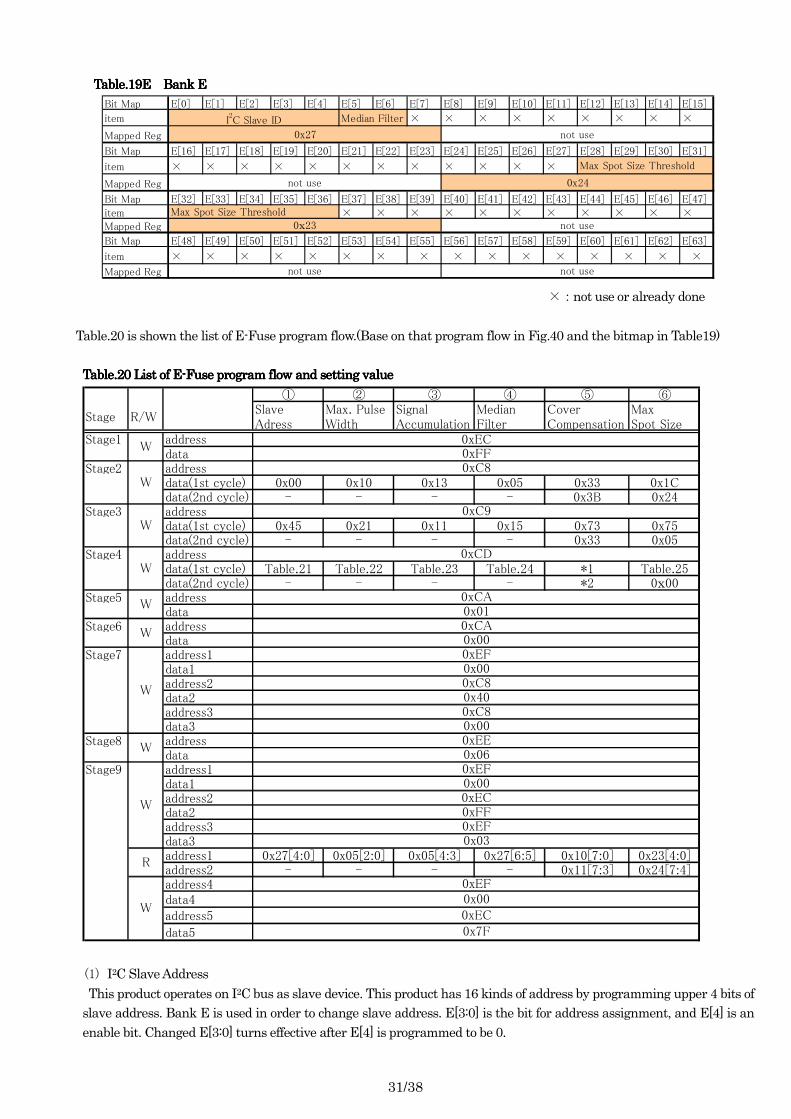
31/38
TaTaTaTable.ble.ble.ble.19191919EEEE Bank EBank EBank EBank E
×:not use or already done
Table.20 is shown the list of E-Fuse program flow.(Base on that program flow in Fig.40 and the bitmap in Table19)
Table.20 List of ETable.20 List of ETable.20 List of ETable.20 List of E----Fuse program flow and setting valueFuse program flow and setting valueFuse program flow and setting valueFuse program flow and setting value
① ② ③ ④ ⑤ ⑥
Stage R/WSlaveAdress
Max. PulseWidth
SignalAccumulation
MedianFilter
CoverCompensation
MaxSpot Size
Stage1 addressdata
Stage2 addressdata(1st cycle) 0x00 0x10 0x13 0x05 0x33 0x1Cdata(2nd cycle) - - - - 0x3B 0x24
Stage3 addressdata(1st cycle) 0x45 0x21 0x11 0x15 0x73 0x75data(2nd cycle) - - - - 0x33 0x05
Stage4 addressdata(1st cycle) Table.21 Table.22 Table.23 Table.24 *1 Table.25data(2nd cycle) - - - - *2 0x00
Stage5 addressdata
Stage6 addressdata
Stage7 address1data1address2data2address3data3
Stage8 addressdata
Stage9 address1data1address2data2address3data3address1 0x27[4:0] 0x05[2:0] 0x05[4:3] 0x27[6:5] 0x10[7:0] 0x23[4:0]address2 - - - - 0x11[7:3] 0x24[7:4]address4data4address5
data5
0xEC0xFF0xC8
0xC9
0xCD
0xCA0x010xCA0x000xEF0x000xC80x400xC80x000xEE0x060xEF0x000xEC
0x000xEC0x7F
0xFF0xEF0x03
0xEF
W
W
W
W
W
R
W
W
W
W
W
(1) I2C Slave Address
This product operates on I2C bus as slave device. This product has 16 kinds of address by programming upper 4 bits of
slave address. Bank E is used in order to change slave address. E[3:0] is the bit for address assignment, and E[4] is an
enable bit. Changed E[3:0] turns effective after E[4] is programmed to be 0.
Bit Map E[0] E[1] E[2] E[3] E[4] E[5] E[6] E[7] E[8] E[9] E[10] E[11] E[12] E[13] E[14] E[15]
item × × × × × × × × ×
Mapped Reg
Bit Map E[16] E[17] E[18] E[19] E[20] E[21] E[22] E[23] E[24] E[25] E[26] E[27] E[28] E[29] E[30] E[31]
item × × × × × × × × × × × ×
Mapped Reg
Bit Map E[32] E[33] E[34] E[35] E[36] E[37] E[38] E[39] E[40] E[41] E[42] E[43] E[44] E[45] E[46] E[47]
item × × × × × × × × × × ×
Mapped Reg
Bit Map E[48] E[49] E[50] E[51] E[52] E[53] E[54] E[55] E[56] E[57] E[58] E[59] E[60] E[61] E[62] E[63]
item × × × × × × × × × × × × × × × ×
Mapped Reg
Max Spot Size Threshold
Max Spot Size Threshold
I2C Slave ID Median Filter
0x27 not use
not use not use
not use 0x24
0x23 not use
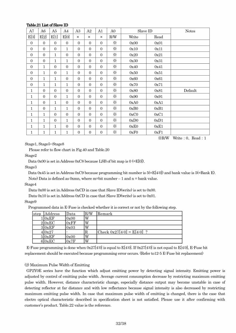
32/38
Table.2Table.2Table.2Table.21111 List of Slave IDList of Slave IDList of Slave IDList of Slave ID
A7 A6 A5 A4 A3 A2 A1 A0 Slave ID Notes
E[3] E[2] E[1] E[0] × × × R/W Write Read
0 0 0 0 0 0 0 ※ 0x00 0x01
0 0 0 1 0 0 0 ※ 0x10 0x11
0 0 1 0 0 0 0 ※ 0x20 0x21
0 0 1 1 0 0 0 ※ 0x30 0x31
0 1 0 0 0 0 0 ※ 0x40 0x41
0 1 0 1 0 0 0 ※ 0x50 0x51
0 1 1 0 0 0 0 ※ 0x60 0x61
0 1 1 1 0 0 0 ※ 0x70 0x71
1 0 0 0 0 0 0 ※ 0x80 0x81 Default
1 0 0 1 0 0 0 ※ 0x90 0x91
1 0 1 0 0 0 0 ※ 0xA0 0xA1
1 0 1 1 0 0 0 ※ 0xB0 0xB1
1 1 0 0 0 0 0 ※ 0xC0 0xC1
1 1 0 1 0 0 0 ※ 0xD0 0xD1
1 1 1 0 0 0 0 ※ 0xE0 0xE1
1 1 1 1 0 0 0 ※ 0xF0 0xF1
※R/W Write:0、Read:1
Stage1, Stage5~Stage8
Please refer to flow chart in Fig.40 and Table.20
Stage2
Data 0x00 is set in Address 0xC8 because LSB of bit map is 0 (=E[0]).
Stage3
Data 0x45 is set in Address 0xC9 because programming bit number is 5(=E[4:0]) and bank value is 5(=Bank E).
Note) Data is defined as 0xmn, where m=bit number – 1 and n = bank value.
Stage4
Data 0x00 is set in Address 0xCD in case that Slave ID(write) is set to 0x00.
Data 0x10 is set in Address 0xCD in case that Slave ID(write) is set to 0x01.
Stage9
Programmed data in E-Fuse is checked whether it is correct or not by the following step.
step Address Data R/W Remark1 0xEF 0x00 W2 0xEC 0xFF W3 0xEF 0x03 W4 0x27 - R Check 0x27[4:0] = E[4:0] ?5 0xEF 0x00 W6 0xEC 0x7F W
E-Fuse programming is done when 0x27[4:0] is equal to E[4:0]. If 0x27[4:0] is not equal to E[4:0], E-Fuse bit
replacement should be executed because programming error occurs. (Refer to12-5 E-Fuse bit replacement)
(2) Maximum Pulse Width of Emitting
GP2Y0E series have the function which adjust emitting power by detecting signal intensity. Emitting power is
adjusted by control of emitting pulse width. Average current consumption decrease by restricting maximum emitting
pulse width. However, distance characteristic change, especially distance output may become unstable in case of
detecting reflector at far distance and with low reflectance because signal intensity is also decreased by restricting
maximum emitting pulse width. In case that maximum pulse width of emitting is changed, there is the case that
electro optical characteristic described in specification sheet is not satisfied. Please use it after confirming with
customer’s product. Table.22 value is the reference.
33/38
Table.2Table.2Table.2Table.22222 Maximum Pulse Width of EmittiMaximum Pulse Width of EmittiMaximum Pulse Width of EmittiMaximum Pulse Width of Emittingngngng
A[18] A[17] A[16] Max. Pulse Width Average current Note
1 1 1 Approx. 320us 26mA Default
1 1 0 Approx. 240us 22mA
1 0 1 Approx. 160us 18mA
1 0 0 Approx. 80us 14mA
0 1 1 Approx. 40us 12mA
Stage1, Stage5~Stage8
Please refer to flow chart in Fig.40 and Table.20
Stage2
Data 0x10 is set in Address 0xC8 because LSB of bit map is 16 (=A[16]).
Stage3
Data 0x21 is set in Address 0xC9 because programming bit number is 3(=A[18:16]) and bank value is 1(=Bank A).
Stage4
Data 0x05 is set in Address 0xCD in case that maximum pulse width is set to 160us.
Data 0x03 is set in Address 0xCD in case that maximum pulse width is set to 40us.
Stage9
Programmed data in E-Fuse is checked whether it is correct or not by the following step.
step Address Data R/W Remark1 0xEF 0x00 W2 0xEC 0xFF W3 0xEF 0x03 W4 0x05 - R Check 0x05[2:0] = A[18:16] ?5 0xEF 0x00 W6 0xEC 0x7F W
E-Fuse programming is done when 0x05[2:0] is equal to A[18:16]. If 0x05[2:0] is not equal to A[18:16], E-Fuse bit
replacement should be executed because programming error occurs. (Refer to12-5 E-Fuse bit replacement)
(3) Signal Accumulation
GP2Y0E series have the function which change the accumulation number of emitting signal. Signal intensity can be
controlled by changing accumulation number. Response time is increased by increasing accumulation number, however
stability of distance output is increased because signal intensity is also increased. In case that signal accumulation
times are changed, there is the case that electro optical characteristic described in specification sheet is not satisfied.
Please use it after confirming with customer’s product. Response time in Table.23 is reference value.
Table.2Table.2Table.2Table.23333 Signal Accumulation NumberSignal Accumulation NumberSignal Accumulation NumberSignal Accumulation Number
A[20] A[19] Accumulation Response Time Note
0 0 1 time 20ms
0 1 5 times 30ms
1 0 30 times 80ms
1 1 10 times 40ms Default
Stage1, Stage5~Stage8
Please refer to flow chart in Fig.40 and Table.20
Stage2
Data 0x13 is set in Address 0xC8 because LSB of bit map is 19 (=A[19]).
Stage3
Data 0x11 is set in Address 0xC9 because programming bit number is 2(=A[20:19]) and bank value is 1(=Bank A).
Stage4
Data 0x00 is set in Address 0xCD in case that signal accumulation is set to 1 time.
Data 0x02 is set in Address 0xCD in case that signal accumulation is set to 30 times.
34/38
Stage9
Programmed data in E-Fuse is checked whether it is correct or not by the following step.
step Address Data R/W Remark1 0xEF 0x00 W2 0xEC 0xFF W3 0xEF 0x03 W4 0x05 - R Check 0x05[4:3] = A[20:19] ?5 0xEF 0x00 W6 0xEC 0x7F W
E-Fuse programming is done when 0x05[4:3] is equal to A[20:19]. If 0x05[4:3] is not equal to A[20:19], E-Fuse bit
replacement should be executed because programming error occurs. (Refer to12-5 E-Fuse bit replacement)
(4) Median Filter
GP2Y0E series have the median calculation function by using several distance outputs in order to get output stable.
Response time increases though distance output gets stable by using median calculation function. Median calculation
number can be selected to 5, 7 or 9. That is, in case of 5, a median of 5 distance values is output after 5 times
measurement. Reference value of response time by combination of accumulation and median filter is shown in Table.24.
In case that median filter function is turned enable, there is the case that electro optical characteristic described in
specification sheet becomes not to be satisfied. Please use it after confirming with customer’s product.
Table.2Table.2Table.2Table.24444 Median FilterMedian FilterMedian FilterMedian Filter
E[6]
E[5]
Data Number
of Median
Response Time (Accumulation) Note
(1time) (5times) (10times) (30times)
0 0 7 30ms 90ms 160ms 430ms
0 1 5 27ms 70ms 120ms 310ms
1 0 9 35ms 110ms 200ms 550ms
1 1 1 20ms 30ms 40ms 80ms Default (10times)
Stage1, Stage5~Stage8
Please refer to flow chart in Fig.40 and Table.20
Stage2
Data 0x05 is set in Address 0xC8 because LSB of bit map is 5 (=E[5]).
Stage3
Data 0x15 is set in Address 0xC9 because programming bit number is 2(=E[6:5]) and bank value is 5(=Bank E).
Stage4
Data 0x00 is set in Address 0xCD in case that data number of median calculation is set to 7.
Data 0x02 is set in Address 0xCD in case that data number of median calculation is set to 9.
Stage9
Programmed data in E-Fuse is checked whether it is correct or not by the following step.
step Address Data R/W Remark1 0xEF 0x00 W2 0xEC 0xFF W3 0xEF 0x03 W4 0x27 - R Check 0x27[6:5] = E[6:5] ?5 0xEF 0x00 W6 0xEC 0x7F W
E-Fuse programming is done when 0x27[6:5] is equal to E[6:5]. If 0x27[6:5] is not equal to E[6:5], E-Fuse bit
replacement should be executed because programming error occurs. (Refer to12-5 E-Fuse bit replacement)
(5) Cover Compensation
Compensation coefficient (k) is measured by the procedure and measurement environment as described in 11-5 cover
compensation k is programmed in C[62:52], and C[51] is enable bit. Programmed C[62:52] turns enable by
35/38
programming 0 in C[51]. There are total 12 bits in programming cover compensation coefficient. It is necessary 2 cycles
shown in 12-3 Program Flow because they are over 8 bits. In case that k is programmed to 350, programmed data is
C[62:51] = 0b001010111100 including enable bit C[51]. So, programmed data at 1st cycle in address 0xCD is 0xBC =
0b10111100 and programmed data at 2nd cycle in address 0xCD is 0x02 = 0b00000010.
1st cycle
Stage1, Stage5~Stage6
Please refer to flow chart in Fig.40 and Table.20
Stage2
Data 0x33 is set in Address 0xC8 because LSB of bit map is 51 (=C[51]).
Stage3
Data 0x73 is set in Address 0xC9 because programming bit number is 8(=C[58:51]) and bank value is 3(=Bank C).
Stage4
Data 0xBC is set in Address 0xCD in case cover compensation coefficient (k) is set to 350.
2nd cycle
Stage1, Stage5~Stage8
Please refer to flow chart in Fig.40 and Table.20
Stage2
Data 0x3B is set in Address 0xC8 because LSB of bit map is 59 (=C[59]).
Stage3
Data 0x33 is set in Address 0xC9 because programming bit number is 4(=C[62:59]) and bank value is 3(=Bank C).
Stage4
Data 0x02 is set in Address 0xCD in case that cover compensation coefficient (k) is set to 350.
Stage9
Programmed data in E-Fuse is checked whether it is correct or not by the following step.
step Address Data R/W Remark1 0xEF 0x00 W2 0xEC 0xFF W3 0xEF 0x03 W4 0x10 - R Check 0x10[7:0] = E[63:56] ?5 0x11 - R Check 0x11[7:3] = E[55:51] ?6 0xEF 0x00 W7 0xEC 0x7F W
E-Fuse programming is done when 0x10[7:0] is equal to E[63:56] and 0x11[7:3] is equal to E[55:51]. If 0x10[7:0] is not
equal to E[63:56] and 0x11[7:3] is not equal to E[55:51], E-Fuse bit replacement should be executed because
programming error occurs. (Refer to12-5 E-Fuse bit replacement)
(6) Maximum Spot Size Threshold of Measurement Error Judgment
Maximum spot size threshold of GP2Y0E series can be set. There is the case that spot size of incomplete reflection
such as the reflection from a fraction of emitting beam and the reflection from the reflective object with complex
boundary line becomes large by deformed spot profile compared with spot size of normal reflection. It has high
possibility that calculated distance by using this incomplete spot profile has large distance error. In order to prevent
decrease of distance accuracy like this, the maximum threshold of spot size can be programmed in E-Fuse. This product
outputs the calculated distance only in case spot size below threshold is detected. Table.25 shows a part of example of
maximum spot size threshold setting. Maximum spot size threshold is set in E[35:28]. E[36] is an enable bit of this
function. Programmed E[35:28] turns enable by changing E[36] to 0. There are total 9bits for maximum spot size
threshold setting. It is necessary 2 cycles in 12-3 Program Flow because they are over 8bits. Measuring data of spot size
can be read out by I2C bus. Please refer to register 0xF8 and 0xF9 (bank0) in register map.
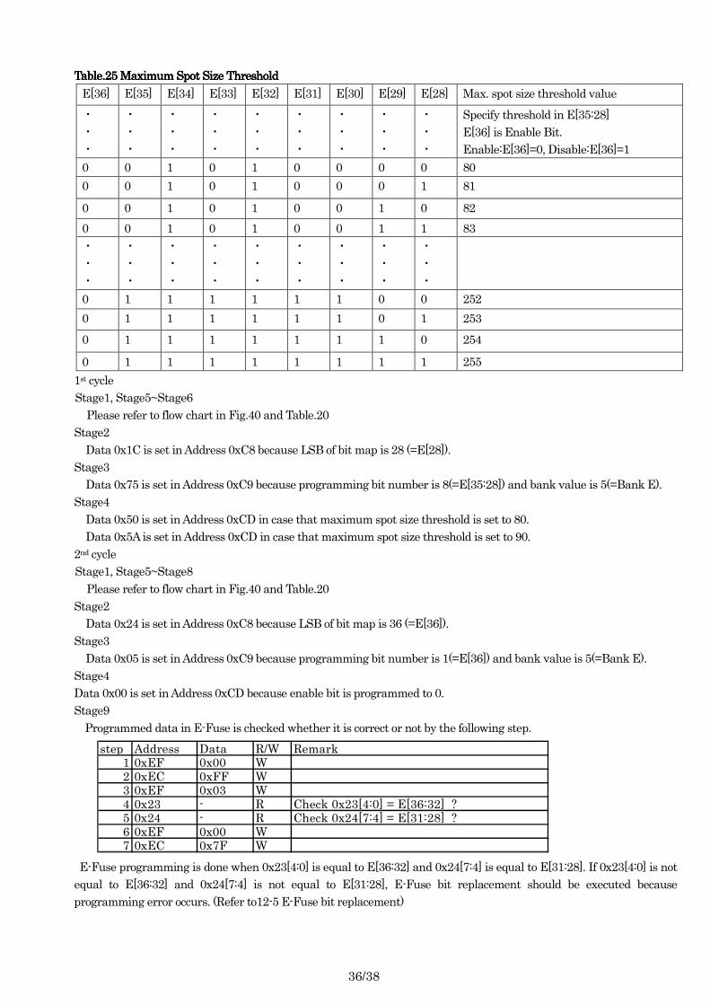
36/38
Table.2Table.2Table.2Table.25555 Maximum Spot Size ThresholdMaximum Spot Size ThresholdMaximum Spot Size ThresholdMaximum Spot Size Threshold
E[36] E[35] E[34] E[33] E[32] E[31] E[30] E[29] E[28] Max. spot size threshold value
・
・
・
・
・
・
・
・
・
・
・
・
・
・
・
・
・
・
・
・
・
・
・
・
・
・
・
Specify threshold in E[35:28]
E[36] is Enable Bit.
Enable:E[36]=0, Disable:E[36]=1
0 0 1 0 1 0 0 0 0 80
0 0 1 0 1 0 0 0 1 81
0 0 1 0 1 0 0 1 0 82
0 0 1 0 1 0 0 1 1 83
・
・
・
・
・
・
・
・
・
・
・
・
・
・
・
・
・
・
・
・
・
・
・
・
・
・
・
0 1 1 1 1 1 1 0 0 252
0 1 1 1 1 1 1 0 1 253
0 1 1 1 1 1 1 1 0 254
0 1 1 1 1 1 1 1 1 255
1st cycle
Stage1, Stage5~Stage6
Please refer to flow chart in Fig.40 and Table.20
Stage2
Data 0x1C is set in Address 0xC8 because LSB of bit map is 28 (=E[28]).
Stage3
Data 0x75 is set in Address 0xC9 because programming bit number is 8(=E[35:28]) and bank value is 5(=Bank E).
Stage4
Data 0x50 is set in Address 0xCD in case that maximum spot size threshold is set to 80.
Data 0x5A is set in Address 0xCD in case that maximum spot size threshold is set to 90.
2nd cycle
Stage1, Stage5~Stage8
Please refer to flow chart in Fig.40 and Table.20
Stage2
Data 0x24 is set in Address 0xC8 because LSB of bit map is 36 (=E[36]).
Stage3
Data 0x05 is set in Address 0xC9 because programming bit number is 1(=E[36]) and bank value is 5(=Bank E).
Stage4
Data 0x00 is set in Address 0xCD because enable bit is programmed to 0.
Stage9
Programmed data in E-Fuse is checked whether it is correct or not by the following step.
step Address Data R/W Remark1 0xEF 0x00 W2 0xEC 0xFF W3 0xEF 0x03 W4 0x23 - R Check 0x23[4:0] = E[36:32] ?5 0x24 - R Check 0x24[7:4] = E[31:28] ?6 0xEF 0x00 W7 0xEC 0x7F W
E-Fuse programming is done when 0x23[4:0] is equal to E[36:32] and 0x24[7:4] is equal to E[31:28]. If 0x23[4:0] is not
equal to E[36:32] and 0x24[7:4] is not equal to E[31:28], E-Fuse bit replacement should be executed because
programming error occurs. (Refer to12-5 E-Fuse bit replacement)
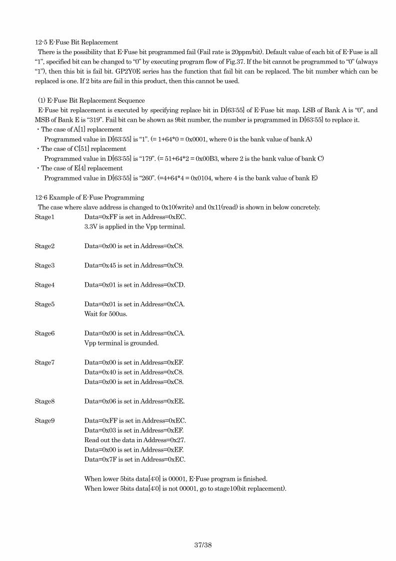
37/38
12-5 E-Fuse Bit Replacement
There is the possibility that E-Fuse bit programmed fail (Fail rate is 20ppm/bit). Default value of each bit of E-Fuse is all
“1”, specified bit can be changed to “0” by executing program flow of Fig.37. If the bit cannot be programmed to “0” (always
“1”), then this bit is fail bit. GP2Y0E series has the function that fail bit can be replaced. The bit number which can be
replaced is one. If 2 bits are fail in this product, then this cannot be used.
(1) E-Fuse Bit Replacement Sequence
E-Fuse bit replacement is executed by specifying replace bit in D[63:55] of E-Fuse bit map. LSB of Bank A is “0”, and
MSB of Bank E is “319”. Fail bit can be shown as 9bit number, the number is programmed in D[63:55] to replace it.
・The case of A[1] replacement
Programmed value in D[63:55] is “1”. (= 1+64*0 = 0x0001, where 0 is the bank value of bank A)
・The case of C[51] replacement
Programmed value in D[63:55] is “179”. (= 51+64*2 = 0x00B3, where 2 is the bank value of bank C)
・The case of E[4] replacement
Programmed value in D[63:55] is “260”. (=4+64*4 = 0x0104, where 4 is the bank value of bank E)
12-6 Example of E-Fuse Programming
The case where slave address is changed to 0x10(write) and 0x11(read) is shown in below concretely.
Stage1 Data=0xFF is set in Address=0xEC.
3.3V is applied in the Vpp terminal.
Stage2 Data=0x00 is set in Address=0xC8.
Stage3 Data=0x45 is set in Address=0xC9.
Stage4 Data=0x01 is set in Address=0xCD.
Stage5 Data=0x01 is set in Address=0xCA.
Wait for 500us.
Stage6 Data=0x00 is set in Address=0xCA.
Vpp terminal is grounded.
Stage7 Data=0x00 is set in Address=0xEF.
Data=0x40 is set in Address=0xC8.
Data=0x00 is set in Address=0xC8.
Stage8 Data=0x06 is set in Address=0xEE.
Stage9 Data=0xFF is set in Address=0xEC.
Data=0x03 is set in Address=0xEF.
Read out the data in Address=0x27.
Data=0x00 is set in Address=0xEF.
Data=0x7F is set in Address=0xEC.
When lower 5bits data[4:0] is 00001, E-Fuse program is finished.
When lower 5bits data[4:0] is not 00001, go to stage10(bit replacement).
38/38
Stage10 The case where the lower 5bits data is 10001 is assumed, and is shown in below flow.
When E[4] is replaced, Data=0x04 is programmed in D[55:62] in 1st cycle and Data=0x01 is
programmed in D[63] in 2nd cycle because programmed value is 260(=0x0104).
Stage10-1 Data=0xFF is set in Address=0xEC.
3.3V is applied in Vpp terminal.
Stage10-2 Data=0x37 is set in Address=0xC8.
Stage10-3 Data=0x74 is set in Address=0xC9.
Stage10-4 Data=0x04 is set in Address=0xCD.
Stage10-5 Data=0x01 is set in Address=0xCA.
Wait for 500us.
Stage10-6 Data=0x00 is set in Address=0xCA.
Vpp terminal is grounded.
Stage10-1’ Data=0xFF is set in Address=0xEC.
3.3V is applied in Vpp terminal.
Stage10-2’ Data=0x3F is set in Address=0xC8.
Stage10-3’ Data=0x04 is set in Address=0xC9.
Stage10-4’ Data=0x01 is set in Address=0xCD.
Stage10-5’ Data=0x01 is set in Address=0xCA.
Wait for 500us.
Stage10-6’ Data=0x00 is set in Address=0xCA.
Vpp terminal is grounded.
Stage10-7 Data=0x00 is set in Address=0xEF.
Data=0x40 is set in Address=0xC8.
Data=0x00 is set in Address=0xC8.
Stage10-8 Data=0x06 is set in Address=0xEE.
Stage10-9 Data=0xFF is set in Address=0xEC.
Data=0x03 is set in Address=0xEF.
Read out the data in Address=0x18 and Address=0x19.
When Data=0x82 in the Address of 0x18 and Data=0 in the address of 0x19[7],
program is finished.
When Data≠0x82 in the Address of 0x18 or Data≠0 in the address of 0x19[7],
it is not possible to correct (=NG).