Embed Size (px)
Citation preview

Polymer Formation in Plasma
• Polymerization (conventional, molecular)• Plasma Polymerization, (atomic)• Competitive Ablation and Polymerization (CAP)• Plasma Sensitivity of Elements• DC Discharge Polymerization• Field Effects• Influence of Wall Contamination

Processes that yield solid depositionfrom gas phase
• Thermal Activation– Chemical Vapor Deposition (CVD)– Hot Wire CVD– Parylene Polymerization*
• Plasma Activation– Plasma Enhanced CVD (PECVD)– Plasma Assisted CVD (PACVD)– Plasma CVD or Plasma Polymerization*
• * Large amount of free radicals are found in the deposition.

2
2
. .
n
CH2 CH2
CH2 CH2
CH2 CH2
CH2 CH2CH2 CH2

Trapped free radicals (dangling bonds) inplasma polymer
-2000.0
-1500.0
-1000.0
-500.0
0.0
500.0
1000.0
1500.0
3B3A3F

Two major mechanisms of polymerization
Chain-Growth Polymerization
Step-growth Polymerization
Molecular PolymerizationNeed specific chemical structures
Building Blocks are monomer molecules
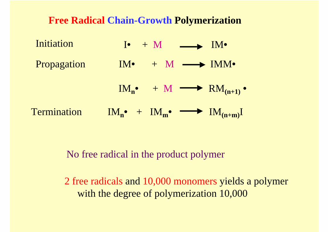
Free Radical Chain-Growth Polymerization
Initiation I• + M IM•
Propagation IM• + M IMM•
IMn• + M RM(n+1) •
Termination IMn• + IMm• IM(n+m)I
No free radical in the product polymer
2 free radicals and 10,000 monomers yields a polymer with the degree of polymerization 10,000

•
•
•
•
•
•••
•
••
•
• •••• ••• ••
∆F = ∆H - T ∆S
S = k ln Ω
−Τ ∆S term is positive for polymerization
∆Η is limited by the difference of bond energies
Polymerization does not proceed in gas phase
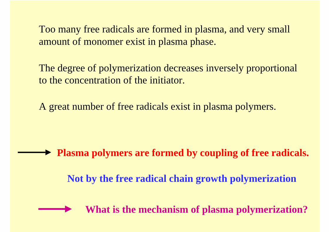
The degree of polymerization decreases inversely proportionalto the concentration of the initiator.
Too many free radicals are formed in plasma, and very small amount of monomer exist in plasma phase.
A great number of free radicals exist in plasma polymers.
Plasma polymers are formed by coupling of free radicals.
Not by the free radical chain growth polymerization
What is the mechanism of plasma polymerization?
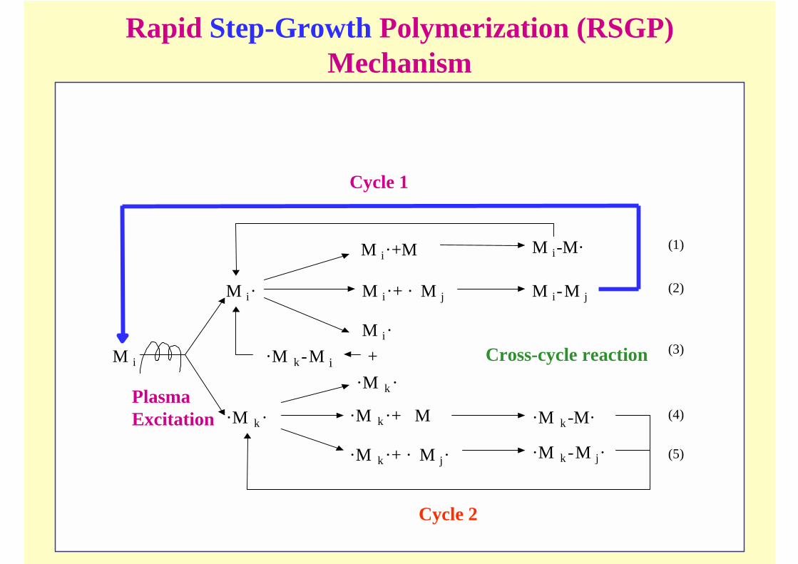
Rapid Step-Growth Polymerization (RSGP)Mechanism
M i
M i·
·M k ·
M i·+ · M j M i-M j
M i·+M M i-M·
M i·
·M k ·
·M k·+ M
·M k·+ · M j·
·M k -M·
·M k -M j·
+·M k-M i
(1)
(2)
(3)
(4)
(5)
Cross-cycle reaction
Cycle 2
Cycle 1
PlasmaExcitation

Plasma Polymerization
• “Atomic” Polymerization– No specific chemical structure is necessary.
• Fragmentation of monomer molecule• Scrambling of atoms• Building Blocks are not the original monomer
molecule, but atoms liberated by thefragmentation of monomer molecule.
• Characteristic deposition rate for each element• Key parameter is W/FM in J/kg.
– W is wattage, F is volume flow rate, and M ismolecular weight.

Typical Operational Range of Plasma Polymerization
• W/FM 10 MJ/kg – 10 GJ/kg• F & W depends on the volume of reactor
– 100 Liter reactor• 1 – 10 sccm• 5 – 100 watts
– The increase of F has the same effect as thedecrease of W, and vise versa.
• Current density in DC polymerization– Less than 1 mA/cm2, V 0.5 – 1.5 kV

Input Energy & Bond Energy
• Input energy is given by W/FM in J/kg.• Specific bond energy of a molecule, which could
be defined as Φ = Σ(bond energy)/M, is given alsoin J/kg.– Ethylene 80 MJ//kg– Tetrafluoroethylene 26 MJ/kg
• When W/FM exceeds ~ 20 times Φ, plasmapolymerization becomes a typical atomicpolymerization, and the molecular structures playlittle role in determining the characteristics ofplasma polymers.
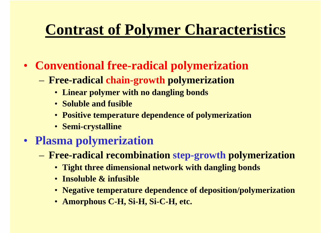
Contrast of Polymer Characteristics
• Conventional free-radical polymerization– Free-radical chain-growth polymerization
• Linear polymer with no dangling bonds• Soluble and fusible• Positive temperature dependence of polymerization• Semi-crystalline
• Plasma polymerization– Free-radical recombination step-growth polymerization
• Tight three dimensional network with dangling bonds• Insoluble & infusible• Negative temperature dependence of deposition/polymerization• Amorphous C-H, Si-H, Si-C-H, etc.
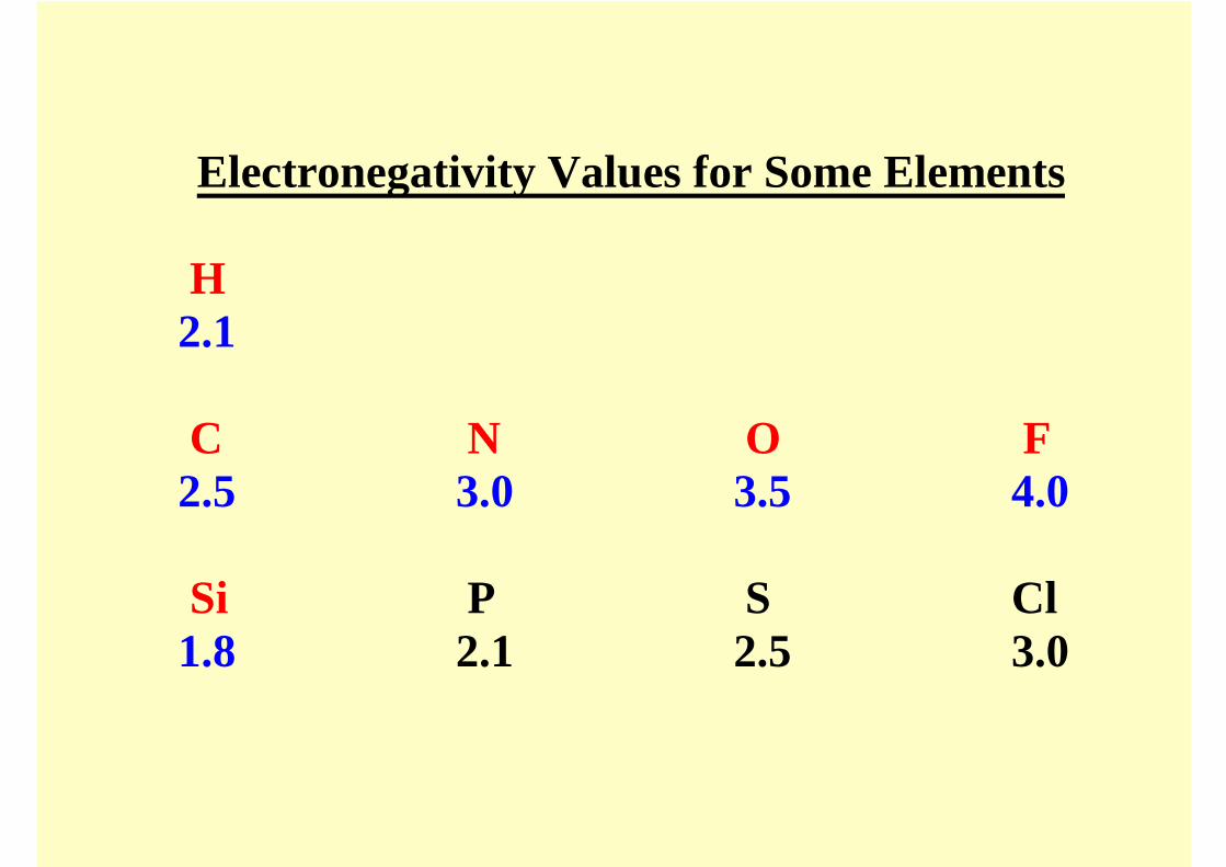
Electronegativity Values for Some Elements
H2.1
C N O F2.5 3.0 3.5 4.0
Si P S Cl1.8 2.1 2.5 3.0

Each Element Has Its Own CharacteristicPolymerization Rate
Normal plasma LTCAT
Ground state atom Positive ion - Negative electronExcited state atom
- +
Cathode Anode
-
-
-
-
-
-
--
Reactive Species in Normal Plasma and LTCAT
Arc generator
SubstrateSubstrate
Cascade Arc Reactor 3e+52e+51e+50e+00.0
0.1
0.2
0.3
0.4MethaneButaneHMDSOTMDSOTMS
W*(FM)c/(FM)m, W
Nor
mal
ized
(DR
), A
/s*s
ccm
CathodeInsulatingMaterial
CoolantChannelMetal
Disk
Anode PlasmaJet
Si
C

H-Si-CH3
CH3
CH3
a-SiHx a-CHx
a-(Si-C)Hx

Total number of gaseous species could increase in spite ofthe deposition of plasma polymers depending on the
fragmentation pattern.
0
20
40
60
80
0 2 4 6 8 10 12 14
Discharge T ime, min
Sys
tem
Pre
ssur
e, m
torr
Plasma on
Plasma off
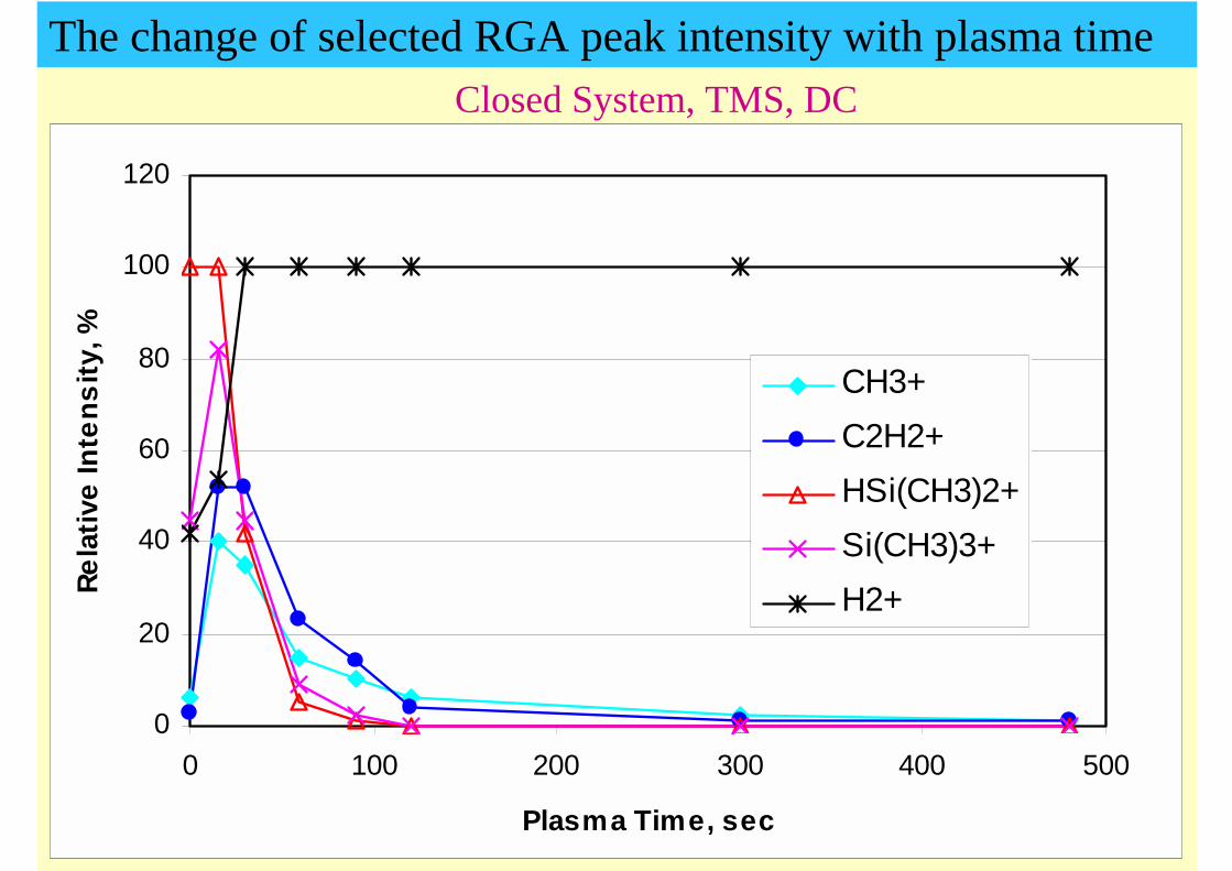
TMS, Closed system, DC
0
20
40
60
80
100
120
0 100 200 300 400 500
Plasma Time, sec
Rela
tive
Inte
nsity
, %
CH3+C2H2+HSi(CH3)2+Si(CH3)3+H2+
The change of selected RGA peak intensity with plasma timeClosed System, TMS, DC

Change of the gas phase species changes thecomposition of plasma deposition
0.0
1.0
2.0
3.0
4.0
5.0
-100 200 500 800 1100 1400 1700 2000
Ar+ Sputter Time (sec)
C/Si
Ato
mic
Rat
io
TcsTfs
TMS, DC, Closed system (cs) and Flow system (fs)

Competitive Ablation and Polymerization(CAP) Principle
• Combination of two observations made in twoprocesses aimed to achieve opposing results.
• Formation of polymers of an etching gas (CF4) inetching of silicon wafer (Kay’s group at IBM).
• Weight loss observed in plasma polymerization of C2F4in high energy input domain (Yasuda’s group at RTI).
• Ablation and polymerization simultaneously occur in aplasma process, but the respective contributiondepends on the conditions of discharge.

STARTING MATERIAL Escaping from the system
StableMoleculesPlasma Phase
(1)
(2)(3)
(4)
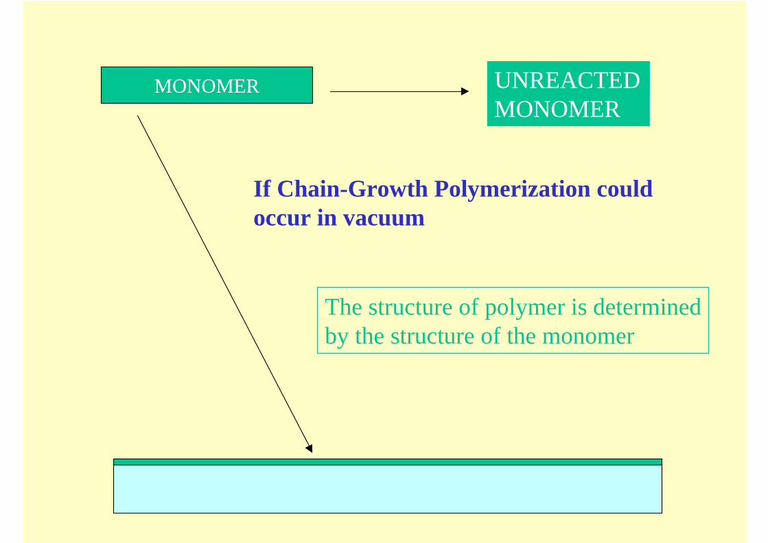
MONOMER
If Chain-Growth Polymerization couldoccur in vacuum
UNREACTEDMONOMER
The structure of polymer is determinedby the structure of the monomer

STARTING MATERIAL
Precursor
NON-POLYMER-FORMING GASES
POLYMERIZATION
Plasma Polymerization by Precursor Concept
iN – Out Rule
Fragmentation of molecules in gas phase and also in solid phase, which contact with plasma, follows the rule of thumb of Nitrogen in and Oxygen out.
Oxygen incorporation into a plasma polymer and that into a plasma-treated polymer are largely due to post-plasma reaction of free radicals with oxygen. Nitrogen has high tendency to be incorporated into a plasma polymer (not in the original forms), and N in a N2 plasma to the treated polymer.
Post-plasma incorporation of N does not occur. N found in a plasma polymer, of which monomer has no N, is due to contamination of the reactor in which N-containing monomer was used.

Plasma Sensitivity Series of Elements
• Ionization of organic molecules does notfollow the same path of ionization of simpleatoms.
• Fragmentation of an organic moleculesprecedes the ionization of fragmentedspecies.
• In-out rule seems to reflect the trends ofplasma fragmentation of organic moleculeswhich contain different elements other thanC and H.

Types of Monomers for Plasma Polymerization
• Nearly all organic and organo-metalliccompounds polymerize in plasma.
• Type 1– Triple bond, aromatic & hetero aromatic
• Type 2– Double bond, cyclic
• Type 3– Linear & branched aliphatic
• Type 4– Oxygen containing aliphatic
Polymerization characteristicsbased on the types of monomers
• Polymerization rate– Type 1 > Type 2 > Type 3 > Type 4
• Photo-emission– Type 4 > Type 3 > Type 2 > Type 1
• Free radicals in polymer substrate– Type 4 > Type 3 > Type 2 > Type 1
• Dangling bonds in plasma polymer– Type 1 > Type 2 > Type 3 > Type 4

Difference of photo-emission at the same energy input level,40 kHz, with magnetic enhancement
TMS TMS+O2
W/FM=722MJ/kg W/FM=762MJ/kg
Type 2 Type 4

Deactivation Photon Emission
Excitation of Deactivation a Plasma Gas Photon Emission
Excitation of Deactivation a Reactive Gas (no emission) Polymerization or Deactivation Surface Modification (no emission)
Correlation between photon emission and polymerization
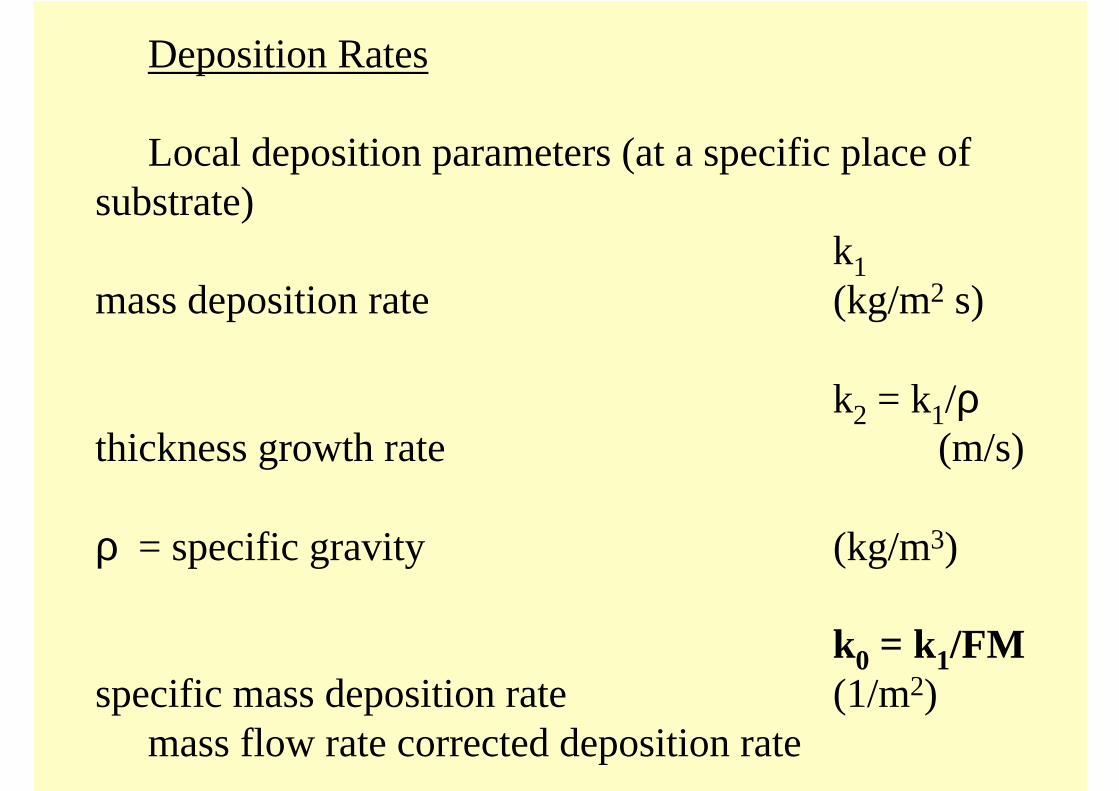
Deposition Rates Local deposition parameters (at a specific place of
substrate)k1
mass deposition rate (kg/m2 s)
k2 = k1/ρthickness growth rate (m/s)
ρ = specific gravity (kg/m3)
k0 = k1/FMspecific mass deposition rate (1/m2)
mass flow rate corrected deposition rate

In the monomer deficient domain
k1 =k’ FM
k1/FM = k’
F: volume or molar flow rate
M: molecular weight of monomer
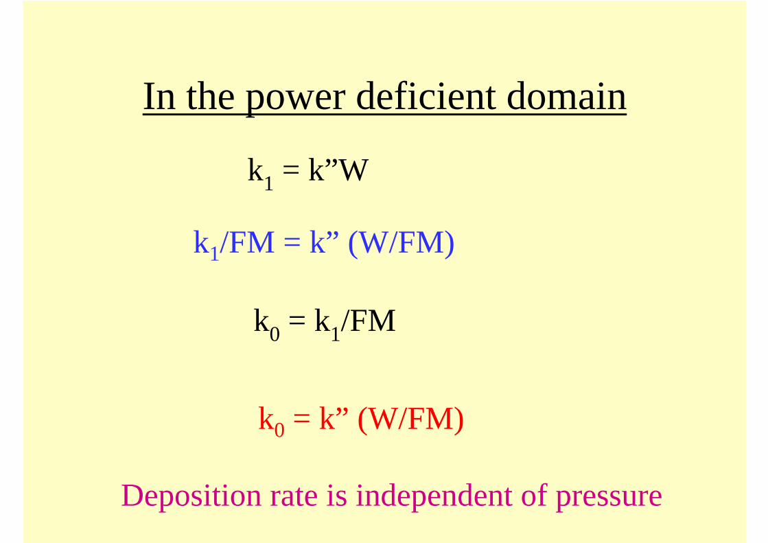
In the power deficient domain
k1 = k”W
k0 = k1/FM
k1/FM = k” (W/FM)
k0 = k” (W/FM)
Deposition rate is independent of pressure

Dependence of deposition rate on operational parametersand domains of plasma polymerization
Dependence of deposition rate of plasma polymer of tetramethyldisiloxane on discharge wattage at the flowing monomerflow rates (cm3/min).
5.7 cm3/min
3.1 cm3/min
1.5 cm3/min
0.82 cm3/min 0.23 cm3/min
Dependence of deposition rate of the plasma polymer of tetramethyldisiloxane on discharge power at a fixed flow rate
120 W
70 W
50 W
20 W
Dependence of deposition rate of the plasma polymer of tetramethyldisiloxane on W/FM at different flow rates
5.7 cm3/min
3.1 cm3/min
1.5 cm3/min
0.82 cm3/min
0.23 cm3/min
Dependence of plasma polymerization domains on deposition rate and W/FM at various flow rates.
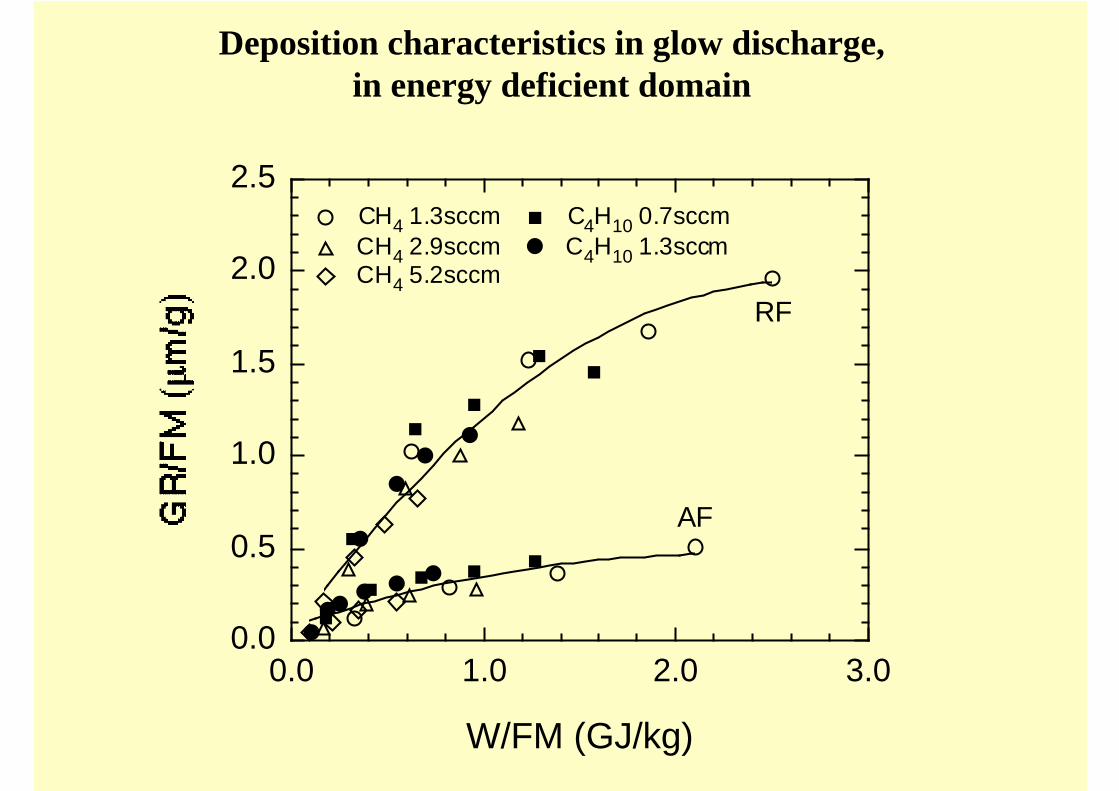
Deposition characteristics in glow discharge,in energy deficient domain
0.0 1.0 2.0 3.0
0.0
0.5
1.0
1.5
2.0
2.5
W/FM (GJ/kg)
RF
AF
CH4 2.9sccmCH4 5.2sccm
CH4 1.3sccm C4H10 0.7sccmC4H10 1.3sccm

Schematic presentation of D.C. glow discharge in a plasma polymerization reactor, (a) System pressure < 6.66 Pa (50 mTorr), (b) > 13.33 Pa (100 mTorr).

Distribution profile of electron temperature in an argon D.C. glow discharge in a plasma polymerization reactor
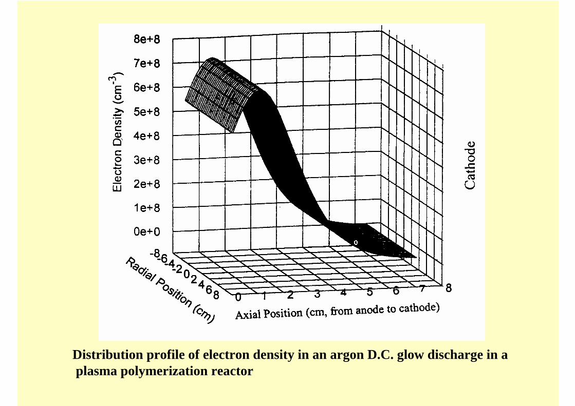
Distribution profile of electron density in an argon D.C. glow discharge in a plasma polymerization reactor
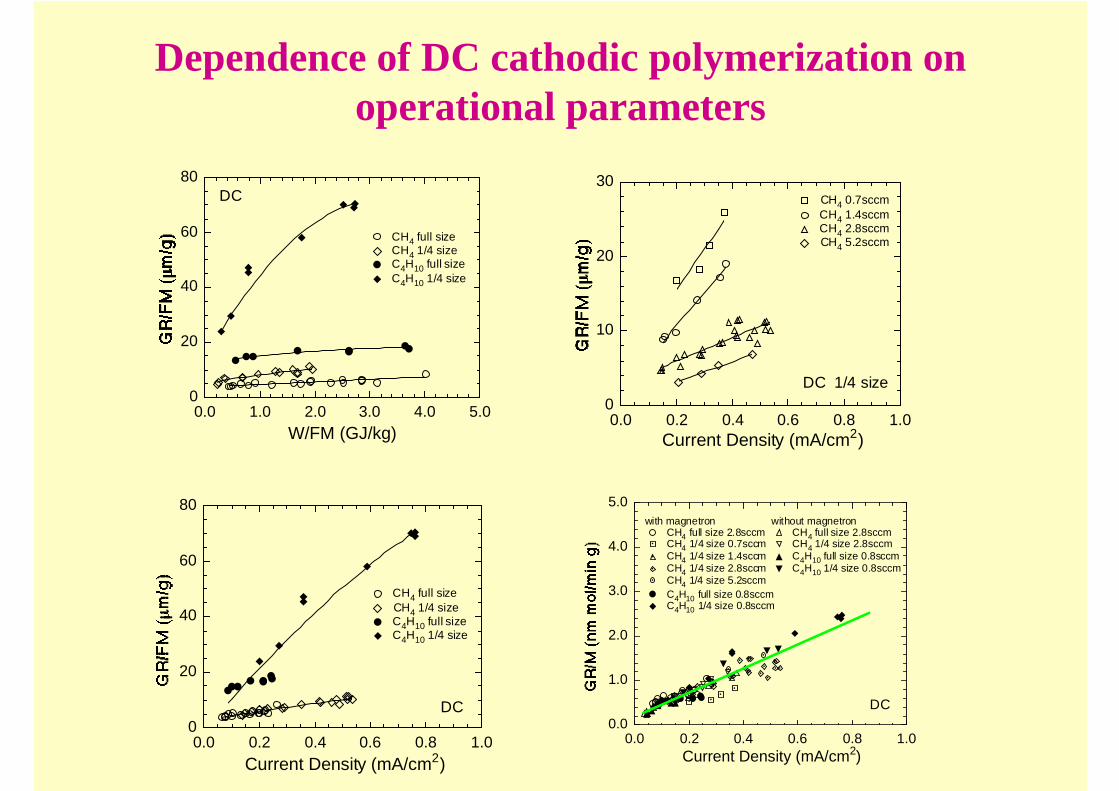
Dependence of DC cathodic polymerization onoperational parameters
0.0 1.0 2.0 3.0 4.0 5.0
0
20
40
60
80
W/FM (GJ/kg)
DC
CH4 full sizeCH4 1/4 size
C4H10 1/4 sizeC4H10 full size
0.0 0.2 0.4 0.6 0.8 1.0
0
10
20
30
Current Density (mA/cm2)
CH4 0.7sccmCH4 1.4sccm
CH4 5.2sccmCH4 2.8sccm
DC 1/4 size
0.0 0.2 0.4 0.6 0.8 1.0
0
20
40
60
80
Current Density (mA/cm2)
DC
CH4 full sizeCH4 1/4 sizeC4H10 full sizeC4H10 1/4 size
0.0 0.2 0.4 0.6 0.8 1.0
0.0
1.0
2.0
3.0
4.0
5.0
Current Density (mA/cm2)
DC
without magnetronwith magnetronCH4 full size 2.8sccmCH4 1/4 size 0.7sccmCH4 1/4 size 1.4sccm
CH4 1/4 size 5.2sccmCH4 1/4 size 2.8sccm
C4H10 full size 0.8sccmC4H10 1/4 size 0.8sccm
CH4 full size 2.8sccmCH4 1/4 size 2.8sccmC4H10 full size 0.8sccmC4H10 1/4 size 0.8sccm
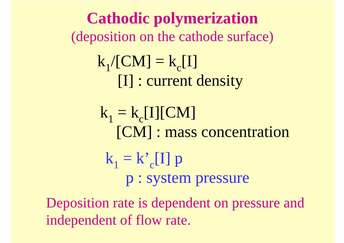
Cathodic polymerization(deposition on the cathode surface)
k1/[CM] = kc[I] [I] : current density
k1 = kc[I][CM] [CM] : mass concentration k1 = k’c[I] p p : system pressure
Deposition rate is dependent on pressure andindependent of flow rate.
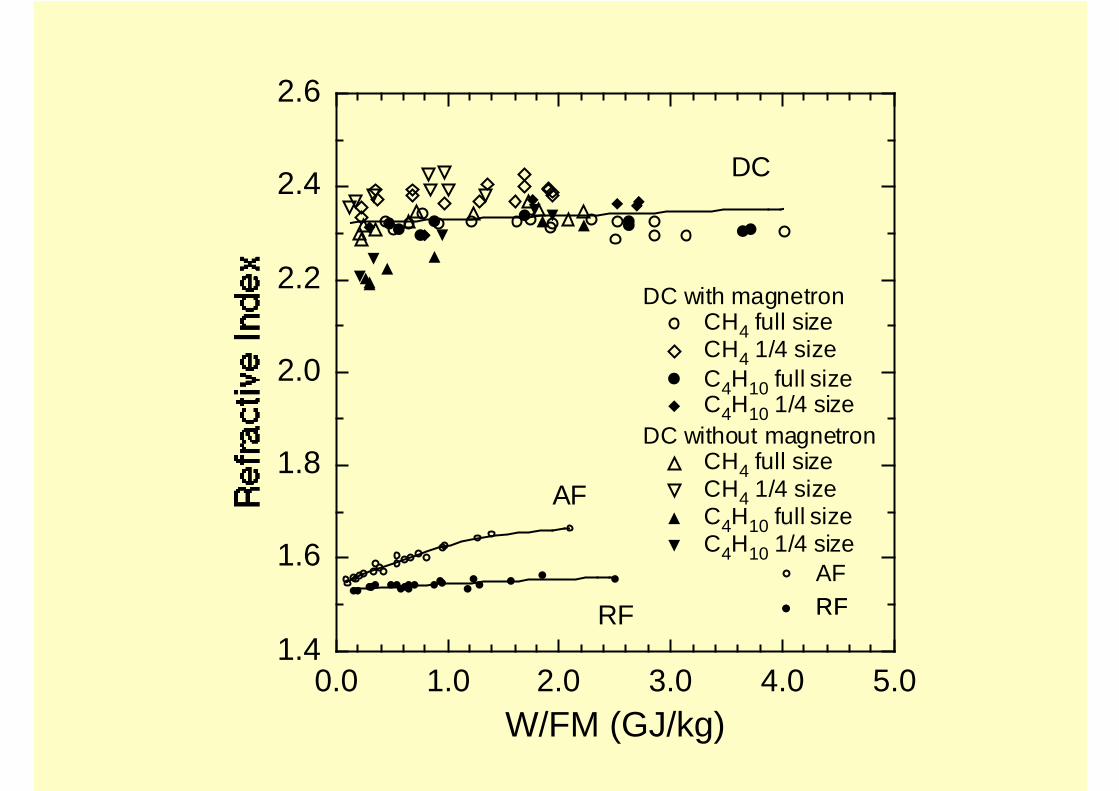
0.0 1.0 2.0 3.0 4.0 5.0
1.4
1.6
1.8
2.0
2.2
2.4
2.6
W/FM (GJ/kg)
DC
AF
RF
DC with magnetron
DC without magnetron
CH4 full sizeCH4 1/4 sizeC4H10 full sizeC4H10 1/4 size
CH4 full sizeCH4 1/4 size
AFC4H10 1/4 sizeC4H10 full size
RFRF
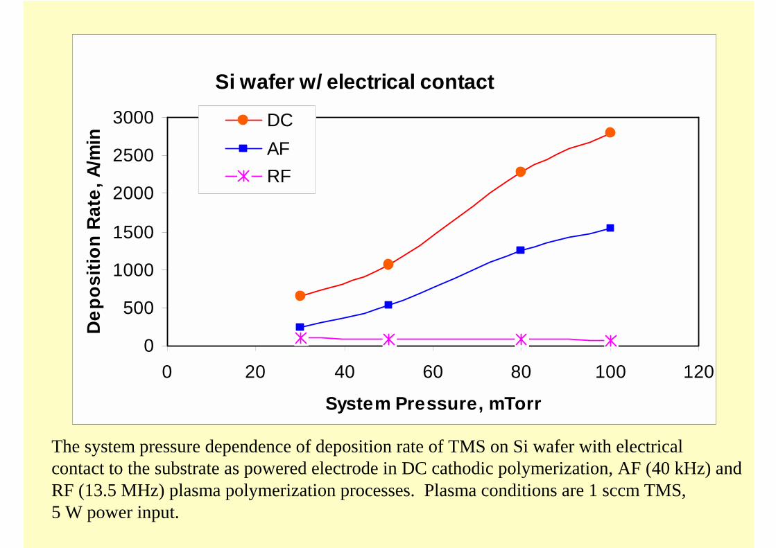
Si wafer w/ electrical contact
0
500
1000
1500
2000
2500
3000
0 20 40 60 80 100 120
System Pressure, mTorr
Dep
ositi
on R
ate,
A/m
inDCAFRF
The system pressure dependence of deposition rate of TMS on Si wafer with electrical contact to the substrate as powered electrode in DC cathodic polymerization, AF (40 kHz) and RF (13.5 MHz) plasma polymerization processes. Plasma conditions are 1 sccm TMS, 5 W power input.
DC
0
500
1000
1500
2000
2500
3000
0 20 40 60 80 100 120
System Pressure, mTorr
Depo
sitio
n Ra
te, A
/min
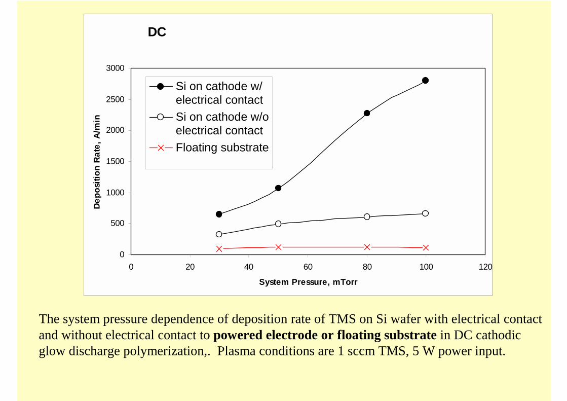
Si on cathode w/electrical contactSi on cathode w/oelectrical contact Floating substrate
The system pressure dependence of deposition rate of TMS on Si wafer with electrical contact and without electrical contact to powered electrode or floating substrate in DC cathodic glow discharge polymerization,. Plasma conditions are 1 sccm TMS, 5 W power input.

DC
1.3
1.4
1.5
1.6
1.7
1.8
1.9
0 20 40 60 80 100 120
System Pressure, mTorrr
Refra
ctiv
e In
dex
Si on cathode w/ electrical contactSi on cathode w/o electrical contact Floating substrate
The system pressure dependence of refractive index of TMS on Si wafer with electrical contact and without electrical contact to powered electrode or floating substrate in DC cathodic glow discharge polymerization,. Plasma conditions are 1 sccm TMS, 5 W power input.

AF
0
500
1000
1500
2000
0 20 40 60 80 100 120
System Pressure, mTorr
Depo
sitio
n Ra
te, A
/min
Si on electrode w/electrical contact Si on electrode w/oelectrical contactFloating substrate
The system pressure dependence of deposition rate of TMS on Si wafer with electrical contact and without electrical contact to powered electrode or floating substrate in AF plasma polymerization processes. Plasma conditions are 1 sccm TMS, 5 W power input.

AF
1.3
1.4
1.5
1.6
1.7
1.8
1.9
0 20 40 60 80 100 120
System Pressure, mTorr
Refra
ctiv
e In
dex
Si on electrode w/ electrical contact Si on electrode w/o electrical contactFloating substrate
The system pressure dependence of refractive index of TMS on Si wafer with electrical contact and without electrical contact to powered electrode or floating substrate in AF plasma polymerization processes. Plasma conditions are 1 sccm TMS, 5 W power input.

RF
0
20
40
60
80
100
0 20 40 60 80 100 120
System Pressure, mTorr
Dep
ositi
on R
ate,
A/m
inSi on electrode w/electrical contact Si on electrode w/oelectrical contactFloating substrate
The system pressure dependence of deposition rate of TMS on Si wafer with electrical contact and without electrical contact to powered electrode or floating substrate in RF plasma polymerization processes. Plasma conditions are 1 sccm TMS, 5 W power input.

RF
1.3
1.4
1.5
1.6
1.7
1.8
1.9
0 20 40 60 80 100 120
System Pressure, mTorr
Ref
ract
ive
Inde
xSi on electrode w/ electrical contact Si on electrode w/o electrical contactFloating substrate
The system pressure dependence of refractive index of TMS on Si wafer with electrical contact and without electrical contact to powered electrode or floating substrate in RF plasma polymerization processes. Plasma conditions are 1 sccm TMS, 5 W power input.
0
50
100
150
200
250
0 20 40 60 80 100 120
System Pressure, mTorr
Dep
ositi
on R
ate,
A/m
in
1
1.2
1.4
1.6
1.8
2
Ref
ract
ive
Inde
x
DR, A/minRefractive Index
On Anode surface
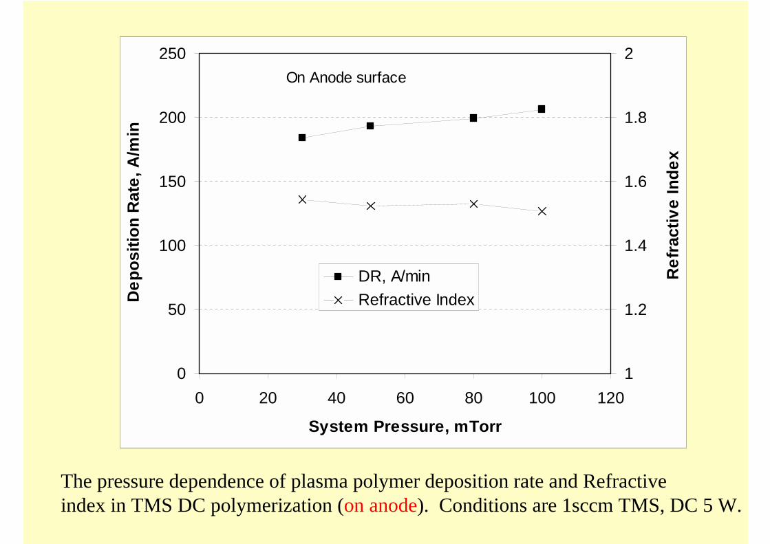
The pressure dependence of plasma polymer deposition rate and Refractive index in TMS DC polymerization (on anode). Conditions are 1sccm TMS, DC 5 W.

0
50
100
150
200
250
-10 -5 0 5 10
(a) Vertical Posistion, cm
Dep
ositi
on R
ate,
A/m
in
50 mTorr100 mTorr
The plasma polymer deposition profile on anode surface in TMS DC cathodic polymerization. Conditions are 1sccm TMS, DC 5 W.

0
200
400
600
800
1000
1200
-10 -5 0 5 10
Vertical Position, cm
Dep
ositi
on R
ate,
A/m
in3 cm
2 cm
15.2 cm Cathode
17.8 cm Anode
7.6 cm Floating Substrate
1/2 piece of Al panel in front of Anode
The effect of the floating panels positioned in front of the anode on the deposition rate on Anode surface and Cathode surface in DC cathodic polymerization. Conditions are: 1 sccm TMS, 50 mTorr, DC 5 W, d = 100 mm.

0
200
400
600
800
1000
1200
-10 -5 0 5 10
Vertical Position, cm
Depo
sitio
n Ra
te, A
/min
3 cm
2 cm
15.2 cm Cathode
17.8 cm Anode
15.2 cm Floating Substrate
1 whole piece of Al panel in front of Anode
The effect of the floating panels positioned in front of the anode on the deposition rate on Anode surface and Cathode surface in DC cathodic polymerization. Conditions are: 1 sccm TMS, 50 mTorr, DC 5 W, d = 100 mm.
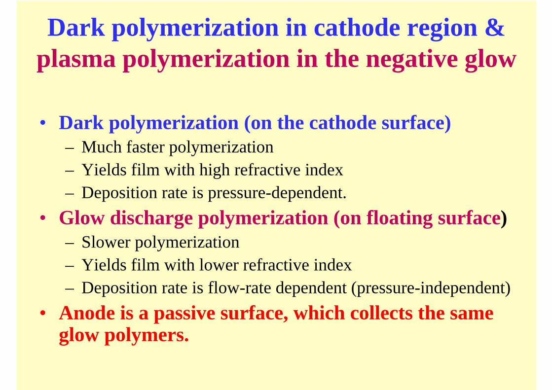
Dark polymerization in cathode region &plasma polymerization in the negative glow
• Dark polymerization (on the cathode surface)– Much faster polymerization– Yields film with high refractive index– Deposition rate is pressure-dependent.
• Glow discharge polymerization (on floating surface)– Slower polymerization– Yields film with lower refractive index– Deposition rate is flow-rate dependent (pressure-independent)
• Anode is a passive surface, which collects the sameglow polymers.

Effect of Electrical Field
• Edge effect– Sputtering by Ar plasma– Deposition on the cathode surface
• Un-balanced surface areas of cathode andanode– Deposition rate onto a small cathode or
powered electrode is higher.• Effect of magnetic confinement
– Reduce the edge effect on sputtering– Over correct the edge-effect in the depositon
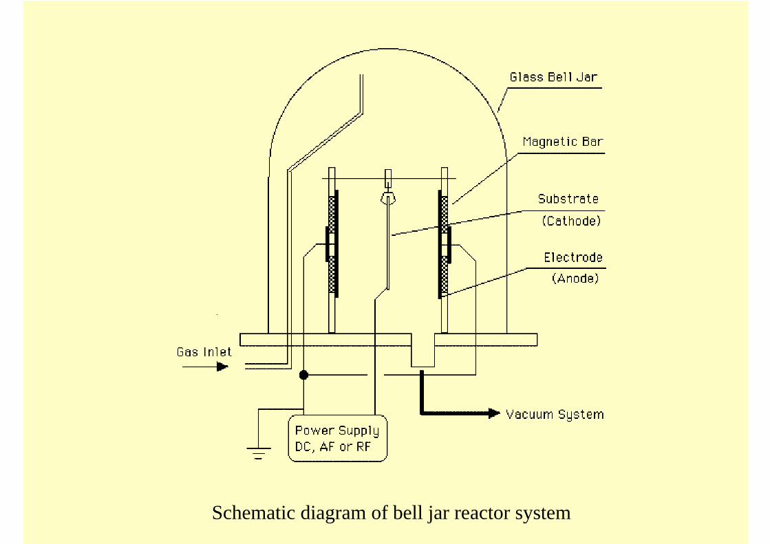
Schematic diagram of bell jar reactor system

Structure of anode magnetron electrode
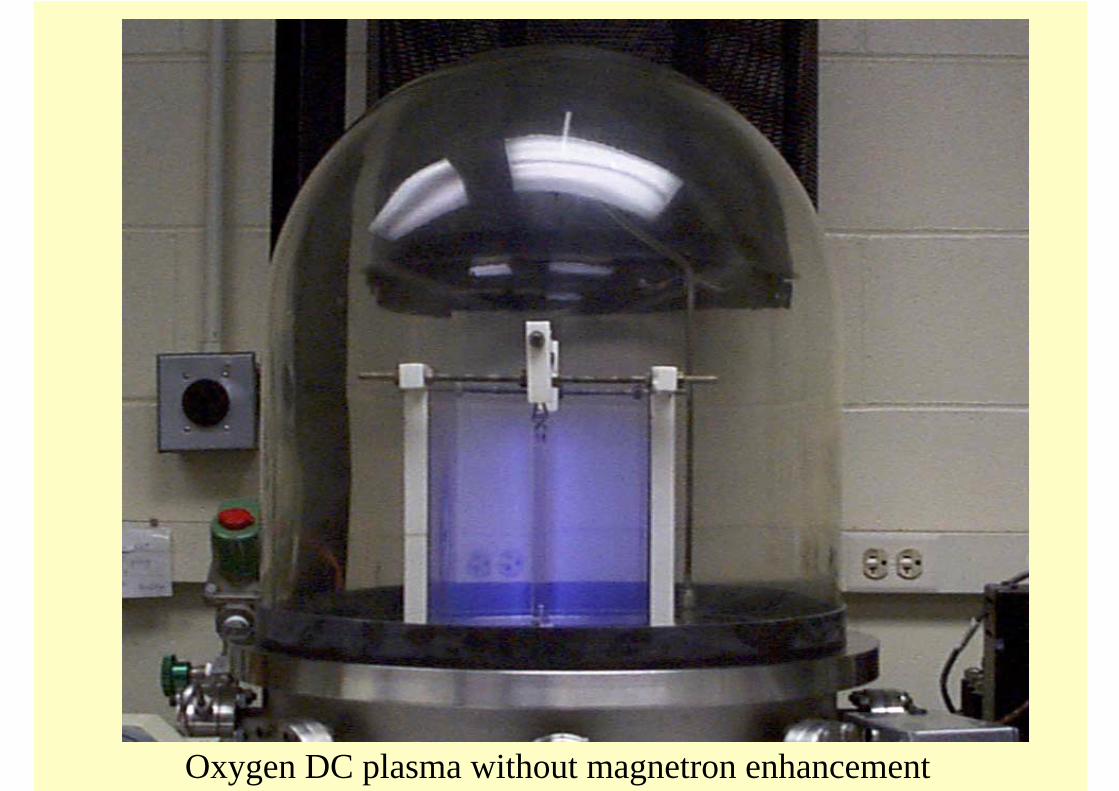
Oxygen DC plasma without magnetron enhancement
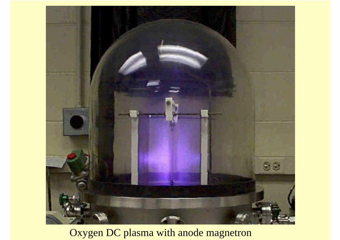
Oxygen DC plasma with anode magnetron
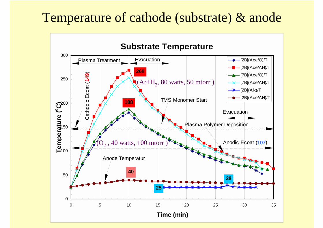
Temperature of cathode (substrate) & anode
Substrate Temperature
0
50
100
150
200
250
300
0 5 10 15 20 25 30 35
Time (min)
Tem
pera
ture
(o C)
[2B](Ace/O)/T
[2B](Ace/AH)/T
[7B](Ace/O)/T
[7B](Ace/AH)/T
[2B](Alk)/T
[2B](Ace/AH)/T
Plasma Treatment Evacuation
TMS Monomer Start
Evacuation
Plasma Polymer Deposition
Anodic Ecoat (107)
Cat
hodi
c Ec
oat (
149) 269
188
28
25
Anode Temperatur
40
(Ar+H2, 80 watts, 50 mtorr )
(O2 , 40 watts, 100 mtorr )

Sputter Cleaning of Cathode Coated with TMS Plasma Polymer

(a): The CRS Panel Coated by TMS Plasma (70 nm)
(b): Interelectrode distance of 50 mm or 75 mm
Cleaned Steel (Fe)
(c): Interelectrode distance of 100 mm to 175 mm
Sputter Cleaning of Cathode Coated with TMS Plasma Polymer

Schematic diagram of different magnetic field configuration. • parallel magnetic field configuration (PM), • (b) opposite magnetic field configuration (OM) and • (c) no magnetron on the backside of anode electrodes.
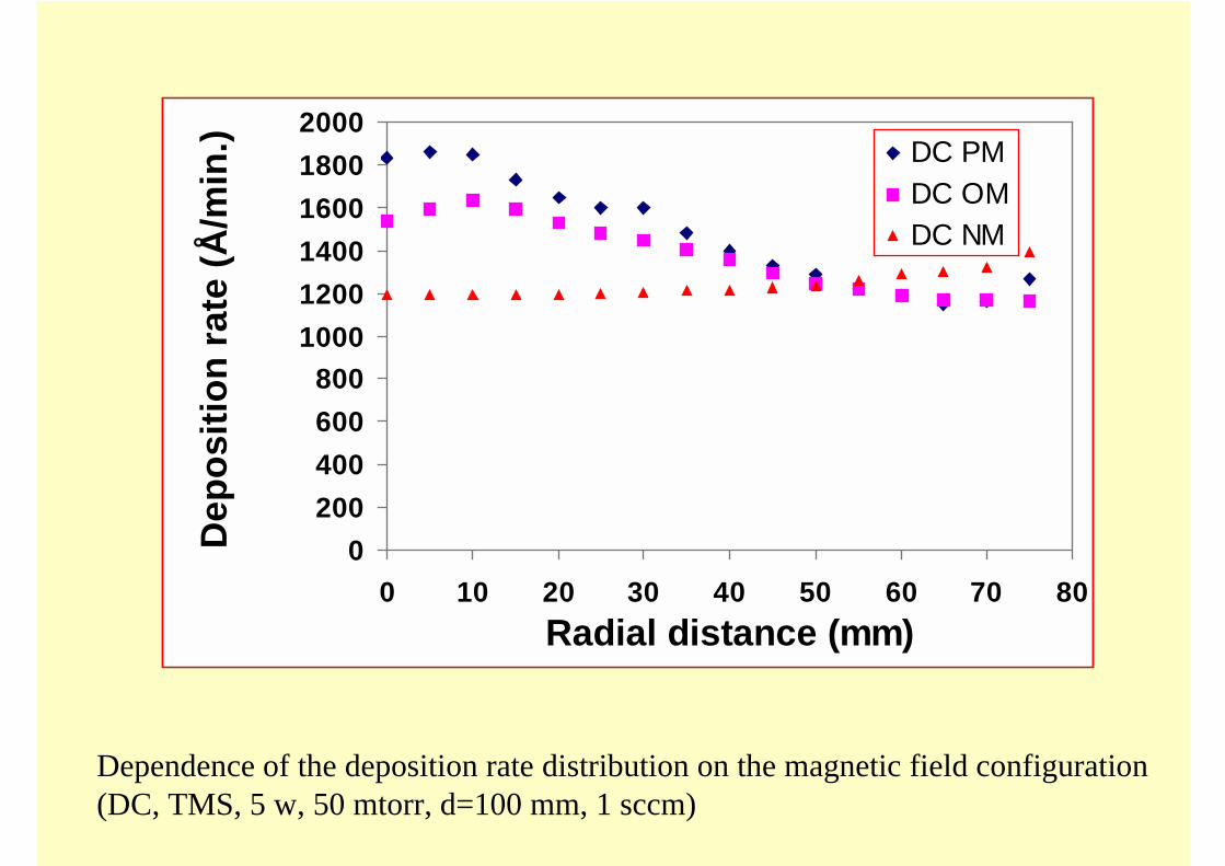
0200400600800
100012001400160018002000
0 10 20 30 40 50 60 70 80Radial distance (mm)
Dep
ositi
on ra
te (Å
/min
.) DC PMDC OMDC NM
Dependence of the deposition rate distribution on the magnetic field configuration (DC, TMS, 5 w, 50 mtorr, d=100 mm, 1 sccm)

0100200300400500600700800900
1000
0 10 20 30 40 50 60 70 80
Radial distance (mm)
Dep
ositi
on ra
te (Å
/min
.)AF PM AF OMAF NM
Dependence of the deposition rate distribution on the magnetic field configuration (AF, TMS, 5 w, 50 mtorr, d=100 mm, 1 sccm)

050
100150200250300350400450500
0 10 20 30 40 50 60 70 80
Radial distance (mm)
Dep
ositi
on ra
te (Å
/min
.) RF, PMRF, OMRF, NM
dependence of the deposition rate distribution on the magnetic field configuration (RF, 5 w, 50 mtorr, d=100 mm, 1 sccm)

0200400600800
100012001400160018002000
0 10 20 30 40 50 60 70 80
Radial distance (mm)
Dep
ositi
on ra
te (Å
/min
.) DCAFRF
Dependence of deposition rate on power supplies (OM, TMS, 50 mtorr, 1 sccm, 5 w, d = 100 mm)

0200400600800
100012001400160018002000
0 20 40 60 80
Radial distance (mm)
Dep
ositi
on ra
te (Å
/min
.) PM, d=100 mmPM, d=80 mmPM, d=60 mmPM, d=40 mmOM, d=100 mmOM, d=80 mmOM, d=60 mmOM, d=40 mm
The influence of electrode distance on the deposition rate (DC. TMS, 50 mtorr, 1 sccm, 5 w)

0
200
400
600
800
1000
1200
1400
0 10 20 30 40 50 60 70 80
Radial distance (mm)
Dep
ositi
on ra
te (Å
/min
.)
AF, PM, d=100mmAF, PM, d=80 mmAF, PM, d=60 mmAF, OM, d=100mmAF, OM, d=80 mmAF, OM, d=60 mmRF, PM, d=100mmRF, PM, d=80 mmRF, PM, d=60 mmRF, OM, d=100 mmRF, OM, d=80 mmRF, OM, d=60 mm
The influence of electrode distance on the deposition rate (AF or RF, TMS, 50 mtorr, 1 sccm, 5 w)
0200400600800
100012001400160018002000
0 10 20 30 40 50 60 70 80Radial distance (mm)
Dep
ositi
on ra
te (Å
/min
.)
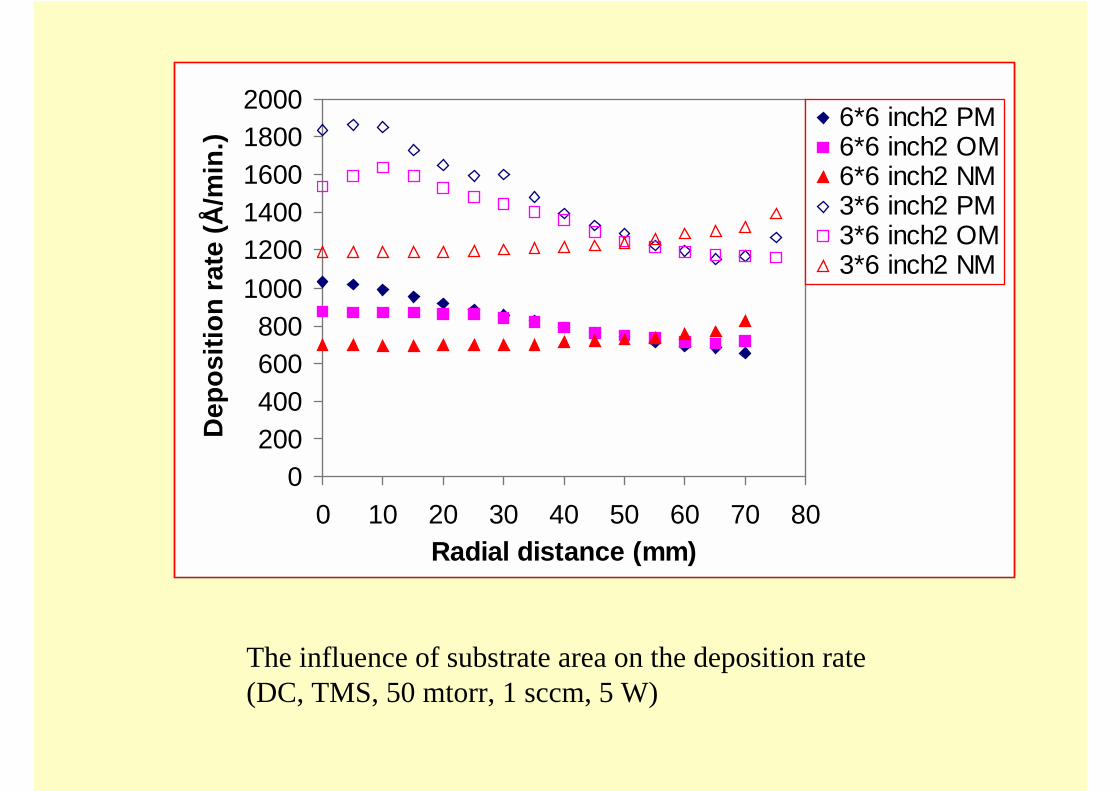
6*6 inch2 PM6*6 inch2 OM6*6 inch2 NM3*6 inch2 PM3*6 inch2 OM3*6 inch2 NM
The influence of substrate area on the deposition rate (DC, TMS, 50 mtorr, 1 sccm, 5 W)

0100200300400500600700800900
0 10 20 30 40 50 60 70 80Radial distance (mm)
Dep
ositi
on ra
te (Å
/min
.)
6*6 inch2 PM6*6 inch2 OM6*6 inch2 NM3*6 inch2 PM3*6 inch2 OM3*6 inch2 NM
The influence of substrate area on the deposition rate (AF, TMS, 50 mtorr, 1 sccm, 5 W)

0
500
1000
1500
2000
2500
0 10 20 30 40 50 60 70 80Radial distance (mm)
Dep
ositi
on ra
te (Å
/min
.) p=30 mtorr,OMp=50 mtorr,OMp=100 mtorr,OMp=30 mtorr,NMp=50 mtorr,NMp=100 mtorr,NM
Dependence of deposition rate distribution on system pressureDC glow discharge (TMS, 5 W, d=100 mm, 1 sccm)

0
200
400
600
800
1000
1200
1400
1600
0 10 20 30 40 50 60 70 80
Radial distance (mm)
Dep
ositi
on ra
te (Å
/min
.) p=30 mtorr,OMp=50 mtorr,OMp=100 mtorr,OMp=30 mtorr,NMp=50 mtorr,NMp=100 mtorr,NM
dependence of deposition rate distribution on system pressureAF glow discharge (TMS, 5 W, d=100 mtorr, 1 sccm).

0
200
400
600
800
1000
1200
1400
0 10 20 30 40 50 60 70 80
Vertical Position, mm
Depo
sitio
n Ra
te, A
/min
d = 60 mmd = 100 mmd = 160 mmno anode assembly
The influence of electrode distance on the deposition rate on Cathode surface in DCcathodic polymerization. Conditions are: 1 sccm TMS, 50 mTorr, DC 5 W, d is the distancebetween two anodes (the cathode is placed in the middle of the two anodes).

Effect of Wall Contamination
• Because of CAP principle, wall contaminationcould change the deposition pattern.
• Elements with high electro negativity in thewall contamination cause the most pronouncedchange in the deposition.– Change from the super adhesion system to no
adhesion system caused by F containing wallcontaminants.

Scanned image of the surface of two alloy panels showing adhesion failure caused by theomission of O2 plasma treatment of the substrate prior to plasma film deposition andapplication of the primer (Deft 44-GN-72 MIL-P-85582 Type I Waterbased ChromatedControl Primer). a) Panel after Skydrol LD4® fluid resistance test, which had the O2 plasmatreatment prior to film deposition and primer application. b) Panel after scribed wet (24-hour immersion in tap water) tape test, which had not been treated with the O2 plasmatreatment prior to film deposition and primer application.

Sequence of processes in the normal operation
Evac./O2 /TMS /(HFE+H2)/ Evac./ O2 / TMS /(HFE+H2)/
The first batch The second batch
Sequence of Plasma Polymerization
TMS Plasma/(HFE+H2) Plasma
New substrate New substrate

Sequence of processes in the abnormal operation
Evac./TMS /(HFE+H2)/ Evac./ TMS /(HFE+H2)/
The first batch The second batch
Sequence of Plasma Polymerization
(HFE+H2) Plasma/TMS Plasma
New substrate New substrate
Previous batch

Adhesion failure occurred atthe interface of the plasma polymerand the substrate alloy
XPS Analysis
Al alloy
Plasma polymer
Spray primer

0
0.2
0.4
0.6
0.8
1
1.2
1.4
0 500 1000 1500 2000 2500 3000 3500 4000 4500
Ar+ Sputter Time (sec)
Silic
on/C
arbo
n Ra
tioPlasma polymer adhering to metal surface
Delaminated paint
Plasma polymer/metal interface

0
5
10
15
20
25
30
0 5 10 15 20 25 30
Date of Sample Preparation, days
Appr
oxim
ate
Fluo
rine
Atom
ic %
O2 or Ar plasma treated no plasma treatment
Liquid N2 TrapReactor Cleaned
Pump Oil Changed
HFE Line Disconnected

Formation of stable molecules in plasma• Stable molecules escape from the system.• Stable molecules shorten the kinetic-path
length of plasma polymerization.– Increase the oligomer content in plasma polymer.– Change elemental composition of plasma polymer.
• Stable molecules formation change the balanceof ablation and polymerization.– Stable molecules formation such as SiF4 is the basis
for plasma etching of silicon, and HF forpolymerization of etching gas.
– Depending the source of element to form stablemolecules, adhesion and/or barrier characteristics ofplasma polymer could be completely damaged.
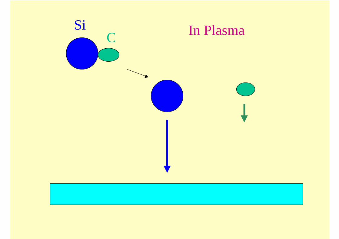
SiC In Plasma

Placing a new substrate in a contaminated reactor
Reactor Wall
SubstrateF
C

Evacuation of Reactor
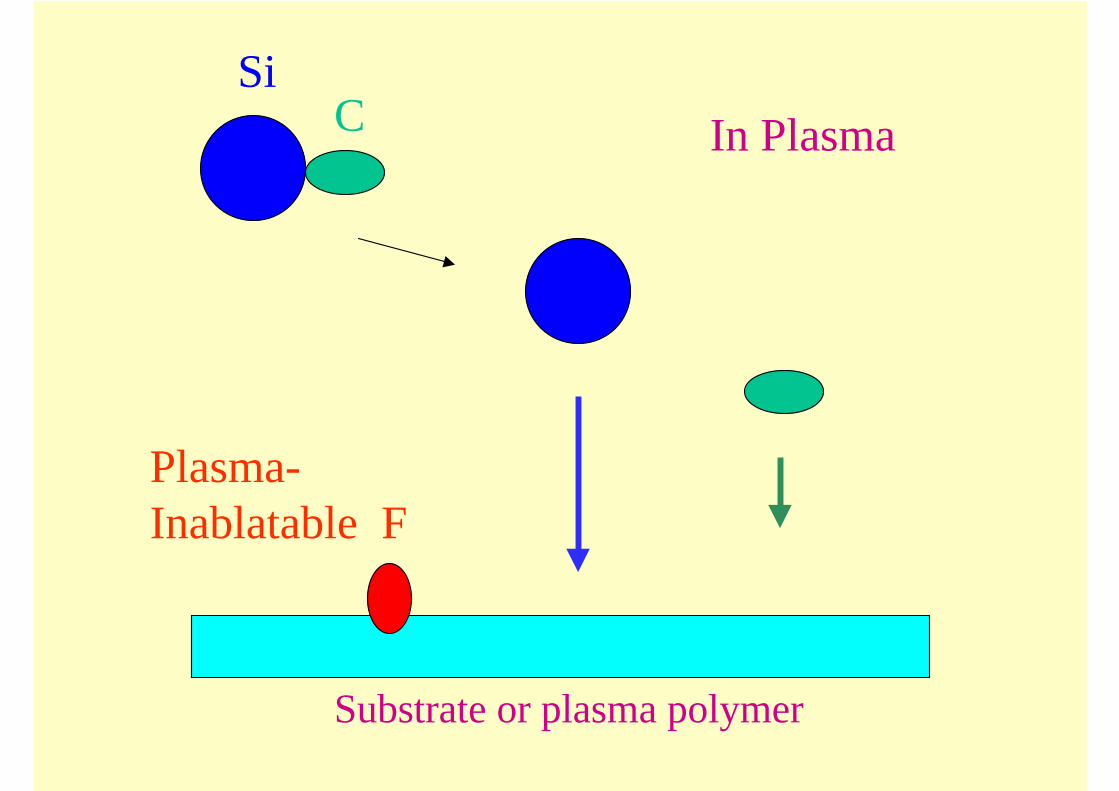
Reactor Wall
Substrate
Migration of oligomeric contaminants, and chemi-sorption on the substrate

Si C
FC
In Plasma

FC
O2
CO2
O2 plasma treatment of contaminated substrate
Substrate or plasma polymer
SiC
Plasma-Inablatable F
In Plasma