Embed Size (px)
Citation preview

ISSN 1345-3041
Mar. 2006 Vol.113
Power Electronics Technology

–
•
•
•
•
•
E
MITSUBISHI ELECTRIC ADVANCMar. 2006 / Vol. 113Cover Story
Power electronics technology is a key tool for helping to solve energy problems and environmental issues, and is widely used throughout modern society.
This feature issue introduces the latest technologies in such areas as power device applications, power conversion and motor control.
Editorial-Chief Yoshikazu Mishima
Editorial Advisors Chisato Kobayashi Yasuyuki Sano Hisao Okamoto Junichi Kitsuki Yukio Kurohata Masayuki Masuda Hiroshi Hasegawa Hiroshi Muramatsu Kazuhisa Hemmi Fuminobu Hidani Hiroshi Yamaki Itsuo Seki Osamu Matsumoto Kazumasa Mitsunaga
Vol. 113 Feature Articles Editor Masato Koyama
Editorial Inquiries Hisao Okamoto Corporate Total Productivity Management & Environmental Programs Fax +81-3-3218-2465
Technological Inquiries Masato Koyama Power Electronics System Development Center Advanced Technology R&D Center Fax +81-6-6497-7288
Mitsubishi Electric Advance is published on line quarterly (in March, June, September, and December) by Mitsubishi Electric Corporation. Copyright © 2006 by Mitsubishi Electric Corporation; all rights reserved. Printed in Japan.
Power Electronics Technology
CONTENTS
Technical Reports Overview ............................................................................................1 by Masato Koyama High-precision Modeling of Motors.................................................2 by Masahiro Kimata and Haruyuki Kometani Gradationally Controlled Voltage Inverter and Its Applications ...6 by Akihiko Iwata and Hiromitsu Takahashi Electromagnetic Noises from Power Devices and Filter Design..9 by Akinori Nishizawa and Satoshi Azuma Evaluation of Fatigue Life Reliability and New Lead Bonding Technology for Power Modules .....................................................13 by Toshihiro Matsunaga and Shingo Sudo SiC Devices and Their Application Technologies ......................17 by Shin-ichi Kinouchi and Masayuki Imaizumi Technologies of Power Electronics for Air Conditioner and Household Electric Appliances .....................................................20 by Mamoru Kawakubo and Masaaki Yabe

*Advanced Technology R&D Center Mitsubishi Electric ADVANCE March 2006 1
TECHNICAL REPORTS
Overview
Author: Masato Koyama*
Power electronics equipment as presented by inverters that generate variable amplitude variable frequency AC voltages, is contributing to energy savings, increased performance, and enhanced functionality in all kinds of areas such as household electric appliances, industry, transportation, and electric power systems. Furthermore, owing to global environmental problems such as global warming and environmental pollution as well as the increasingly critical energy situation across the world in recent years, expectations are rising for power electronics equipment that makes it possible to use clean power and produces impressive energy savings.
As a producer of power electronics products ranging from power semiconductor devices to power converters and systems for a wide variety of applications, Mitsubishi Electric Corporation has been pioneering the development of power electronics technology.
Major market needs for power electronics equipment include downsizing, improved efficiency, enhanced performance, increased reliability and environmental friendliness. This feature edition introduces the latest power electronics technologies that Mitsubishi Electric Corporation has developed over the years in line with market needs. These technologies encompass power semiconductor devices, power conversion, motor control, and integration.
TECHNICAL REPORTS
High-precision Modeling of Motors Authors: Masahiro Kimata* and Haruyuki Kometani*
The control performance of power electronics equipment for variable speed motor drive has been improving each year. For example, the variable-speed range of general-purpose inverters has increased ap-proximately ten-fold in the past 15 years. Although this has relied on advances in hardware such as CPUs, power semiconductor devices and sensors, motor control technology has also improved. The progress of motor control technology translates into improving the precision of motor models.
One way to improve the precision of such models is to consider coordination with electromagnetic field analysis and motor structure. This paper reviews how we have developed high-precision models and motor control.
1. Motor Control and Models 1.1 Motor control scheme
As a simple example of how motor control works, we consider the control scheme for induction motors. The simplest induction-motor control scheme is con-stant-V/f control. While frequency (f) is being varied, the exciting current is kept constant such that the ratio of output voltage (V) to f remains constant. Under this constant-V/f control, an induction motor can be mod-eled as exciting inductance and rotor resistance alone without considering transient terms. This is a simplified representation of the T-type equivalent circuitry which is known as an equivalent induction-motor circuit model under steady state. Since the actual effective voltage decreases due to a voltage drop in the stator winding, which was ignored in constructing the model, the char-acteristics of constant-V/f control deteriorate particularly at low speed.
Fig. 1 Induction motor models
In contrast to the above, vector control uses a mo-
tor circuit equation as a motor model. For example, modeling on the stationary stator d-q axis in Cartesian coordinates is expressed in the form of the following equation.
vds
vqs
00
⎛
⎝
⎜ ⎜ ⎜ ⎜
⎞
⎠
⎟ ⎟ ⎟ ⎟
=
Rs + PLs 0 PM 00 Rs + PLs 0 PM
PM ω re M Rr + PLr ω reLr
−ωre M PM −ω reLr Rr + PLr
⎛
⎝
⎜ ⎜ ⎜ ⎜
⎞
⎠
⎟ ⎟ ⎟ ⎟
ids
iqs
idr
iqr
⎛
⎝
⎜ ⎜ ⎜ ⎜
⎞
⎠
⎟ ⎟ ⎟ ⎟
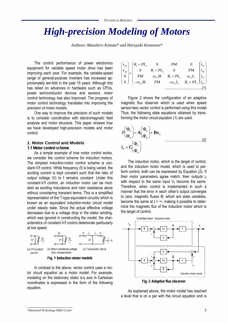
......................................(1) Figure 2 shows the configuration of an adaptive
magnetic flux observer which is used when speed sensor-less vector control is performed using this model. Thus, the following state equations obtained by trans-forming the motor circuit equation (1) are used.
PΦs
Φr
⎛
⎝ ⎜
⎞
⎠ ⎟ = A
Φs
Φr
⎛
⎝ ⎜
⎞
⎠ ⎟ + Bvs
is = CΦs
Φr
⎛
⎝ ⎜
⎞
⎠ ⎟
......................................(2)
The induction motor, which is the target of control,
and the induction motor model, which is used to per-form control, both can be expressed by Equation (2). If their motor parameters agree match, their outputs is with respect to the same input Vs become the same. Therefore, when control is implemented in such a manner that the error in each other’s output converges to zero, magnetic fluxes Φ, which are state variables, become the same at t = ∞, making it possible to deter-mine the magnetic flux of the induction motor which is the target of control.
Fig. 2 Adaptive flux observer
As explained above, the motor model has reached
a level that is on a par with the circuit equation and is
*Advanced Technology R&D Center 2
TECHNICAL REPORTS
almost perfect. However, as market demands become increasingly sophisticated, further improvements and developments are still being made.
1.2 Auto tuning
As is evident from the previous section, as the method of control becomes more sophisticated, more accurate motor parameters are required. To determine the correct motor parameters, auto tuning is performed. Off-line auto tuning refers to a function with which the inverter measures motor parameters off-line by itself and stores the results. When the motor is driven using the motor parameters measured by the off-line auto tuning function, the motor generates loss-induced heat.
Temperature differences between the measured and actual motor deteriorate control performance. On-line auto tuning, which tunes motor parameters at the time of motor startup, is an effective way to counter this.
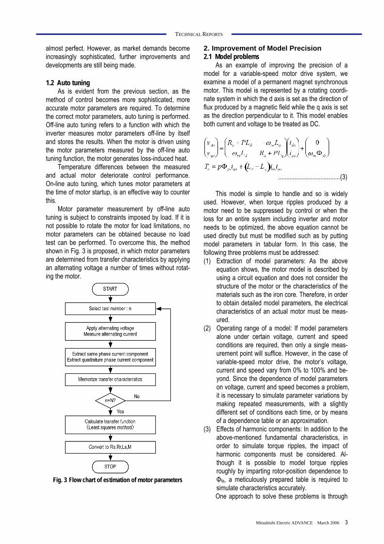
Motor parameter measurement by off-line auto tuning is subject to constraints imposed by load. If it is not possible to rotate the motor for load limitations, no motor parameters can be obtained because no load test can be performed. To overcome this, the method shown in Fig. 3 is proposed, in which motor parameters are determined from transfer characteristics by applying an alternating voltage a number of times without rotat-ing the motor.
Fig. 3 Flow chart of estimation of motor parameters
2. Improvement of Model Precision 2.1 Model problems
As an example of improving the precision of a model for a variable-speed motor drive system, we examine a model of a permanent magnet synchronous motor. This model is represented by a rotating coordi-nate system in which the d axis is set as the direction of flux produced by a magnetic field while the q axis is set as the direction perpendicular to it. This model enables both current and voltage to be treated as DC.
......................................(3) This model is simple to handle and so is widely
used. However, when torque ripples produced by a motor need to be suppressed by control or when the loss for an entire system including inverter and motor needs to be optimized, the above equation cannot be used directly but must be modified such as by putting model parameters in tabular form. In this case, the following three problems must be addressed: (1) Extraction of model parameters: As the above
equation shows, the motor model is described by using a circuit equation and does not consider the structure of the motor or the characteristics of the materials such as the iron core. Therefore, in order to obtain detailed model parameters, the electrical characteristics of an actual motor must be meas-ured.
(2) Operating range of a model: If model parameters alone under certain voltage, current and speed conditions are required, then only a single meas-urement point will suffice. However, in the case of variable-speed motor drive, the motor’s voltage, current and speed vary from 0% to 100% and be-yond. Since the dependence of model parameters on voltage, current and speed becomes a problem, it is necessary to simulate parameter variations by making repeated measurements, with a slightly different set of conditions each time, or by means of a dependence table or an approximation.
(3) Effects of harmonic components: In addition to the above-mentioned fundamental characteristics, in order to simulate torque ripples, the impact of harmonic components must be considered. Al-though it is possible to model torque ripples roughly by imparting rotor-position dependence to Φfa, a meticulously prepared table is required to simulate characteristics accurately. One approach to solve these problems is through
Mitsubishi Electric ADVANCE March 2006 3
TECHNICAL REPORTS
coordination with electromagnetic field analysis. By determining the dependence of motor parameters through electromagnetic field analysis, more detailed modeling is possible by using d-q-axis models that takes only the fundamental component into considera-tion.
Table 1 lists the precision improvements for motor models. There are demands for not only improved versions of present d-q-axis models but also for de-tailed motor models that incorporate motor structure and materials properties in the models themselves. Since this detailed model will be used for the control and analysis of a power electronics system, it should allow a control program to be incorporated easily and also facilitate coordination with a control simulator or circuit simulator, similar to existing d-q-axis models. However, specific solutions remain elusive and detailed models are not yet practical, so future developments are awaited.
Table 1 Motor models
Accuracy Motor design method
Motor model Applied to control
Theoretical design
Fundamental compo-nent model
completed
Variable motor pa-rameters depended on operating condition
completedDesign rule learned by experience
Harmonic component model
NOT
Magnetic permeance method
Structure based model NOT
low high
Finite ele-ment method
Finite element method model
NOT
2.2 Coordination with electromagnetic field analysis
The improved precision of motor models through coordination with electromagnetic field analysis dis-cussed in the previous section is producing favorable results. Since it is possible to analyze the flux linkage of a permanent magnet motor under loaded conditions with the help of electromagnetic field analysis, the motor’s inductance can be calculated using the follow-ing voltage equation.
φd = φm − Ld Id
φq = LqIq ......................................(4)
In this case, since it is impossible to separate flux
Φm produced by the magnet and flux LdId induced by d-axis current, the d-axis current is varied minutely in the analysis. Assuming that the effect of magnetic saturation in relation to this minute variation works equally, Φm and flux LdId are separated from two ana-
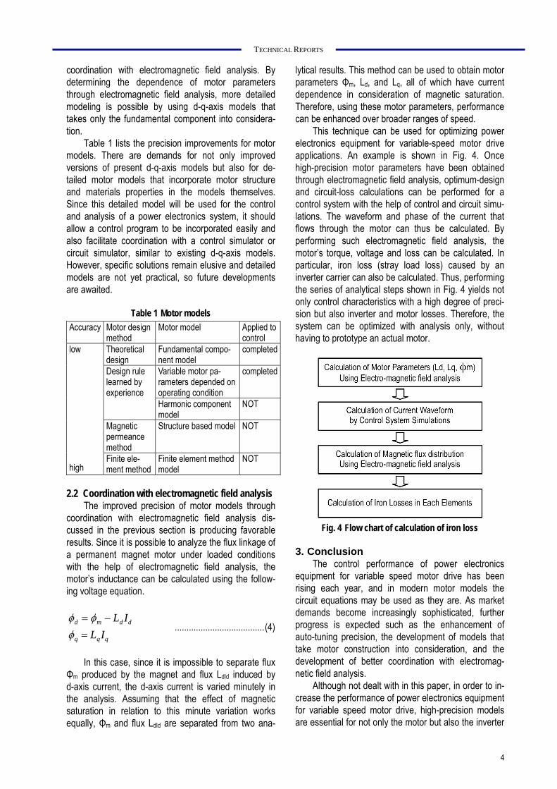
lytical results. This method can be used to obtain motor parameters Φm, Ld, and Lq, all of which have current dependence in consideration of magnetic saturation. Therefore, using these motor parameters, performance can be enhanced over broader ranges of speed.
This technique can be used for optimizing power electronics equipment for variable-speed motor drive applications. An example is shown in Fig. 4. Once high-precision motor parameters have been obtained through electromagnetic field analysis, optimum-design and circuit-loss calculations can be performed for a control system with the help of control and circuit simu-lations. The waveform and phase of the current that flows through the motor can thus be calculated. By performing such electromagnetic field analysis, the motor’s torque, voltage and loss can be calculated. In particular, iron loss (stray load loss) caused by an inverter carrier can also be calculated. Thus, performing the series of analytical steps shown in Fig. 4 yields not only control characteristics with a high degree of preci-sion but also inverter and motor losses. Therefore, the system can be optimized with analysis only, without having to prototype an actual motor.
Fig. 4 Flow chart of calculation of iron loss
3. Conclusion The control performance of power electronics
equipment for variable speed motor drive has been rising each year, and in modern motor models the circuit equations may be used as they are. As market demands become increasingly sophisticated, further progress is expected such as the enhancement of auto-tuning precision, the development of models that take motor construction into consideration, and the development of better coordination with electromag-netic field analysis.
Although not dealt with in this paper, in order to in-crease the performance of power electronics equipment for variable speed motor drive, high-precision models are essential for not only the motor but also the inverter
4

TECHNICAL REPORTS
and amplifier, in order to reduce errors in inverter output voltage. A high-precision load model is also necessary in order to control the behavior of a load driven by the motor.
We are committed to improving the precision of various models and enhancing the performance of our power electronics equipment for variable speed motor drive.
Mitsubishi Electric ADVANCE March 2006 5
TECHNICAL REPORTS
Gradationally Controlled Voltage Inverter and Its Applications
Authors: Akihiko Iwata* and Hiromitsu Takahashi**
We have developed a gradationally controlled volt-age inverter which is capable of outputting a high-precision waveform even at low switching frequen-cies and have succeeded in putting it to practical use. This inverter employs multiple constituent inverters that form a binary or ternary DC voltage ratio with one an-other, and are connected in series to output the com-bined sum of the output voltages of the individual in-verters. The geometry of the resultant output voltage is quasi-sinusoidal.
1. Configuration and features of grada-
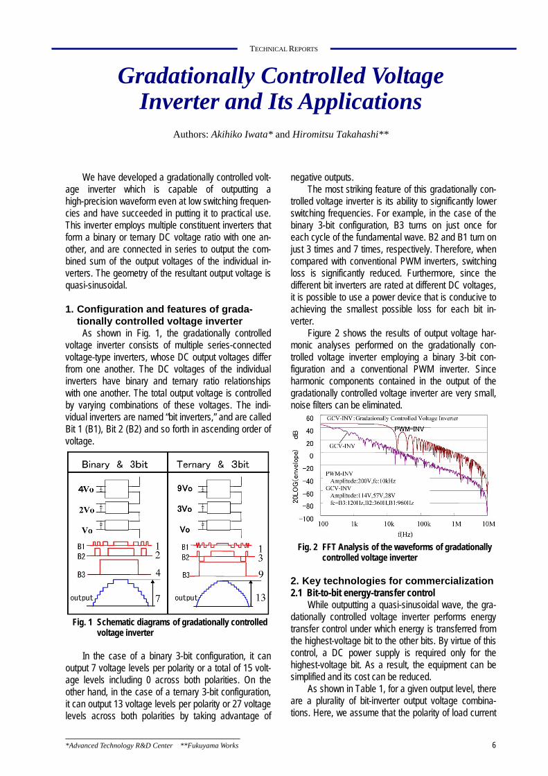
tionally controlled voltage inverter As shown in Fig. 1, the gradationally controlled
voltage inverter consists of multiple series-connected voltage-type inverters, whose DC output voltages differ from one another. The DC voltages of the individual inverters have binary and ternary ratio relationships with one another. The total output voltage is controlled by varying combinations of these voltages. The indi-vidual inverters are named “bit inverters,” and are called Bit 1 (B1), Bit 2 (B2) and so forth in ascending order of voltage.
Fig. 1 Schematic diagrams of gradationally controlled
voltage inverter In the case of a binary 3-bit configuration, it can
output 7 voltage levels per polarity or a total of 15 volt-age levels including 0 across both polarities. On the other hand, in the case of a ternary 3-bit configuration, it can output 13 voltage levels per polarity or 27 voltage levels across both polarities by taking advantage of
negative outputs. The most striking feature of this gradationally con-
trolled voltage inverter is its ability to significantly lower switching frequencies. For example, in the case of the binary 3-bit configuration, B3 turns on just once for each cycle of the fundamental wave. B2 and B1 turn on just 3 times and 7 times, respectively. Therefore, when compared with conventional PWM inverters, switching loss is significantly reduced. Furthermore, since the different bit inverters are rated at different DC voltages, it is possible to use a power device that is conducive to achieving the smallest possible loss for each bit in-verter.
Figure 2 shows the results of output voltage har-monic analyses performed on the gradationally con-trolled voltage inverter employing a binary 3-bit con-figuration and a conventional PWM inverter. Since harmonic components contained in the output of the gradationally controlled voltage inverter are very small, noise filters can be eliminated.
Fig. 2 FFT Analysis of the waveforms of gradationally
controlled voltage inverter
2. Key technologies for commercialization 2.1 Bit-to-bit energy-transfer control
While outputting a quasi-sinusoidal wave, the gra-dationally controlled voltage inverter performs energy transfer control under which energy is transferred from the highest-voltage bit to the other bits. By virtue of this control, a DC power supply is required only for the highest-voltage bit. As a result, the equipment can be simplified and its cost can be reduced.
As shown in Table 1, for a given output level, there are a plurality of bit-inverter output voltage combina-tions. Here, we assume that the polarity of load current
*Advanced Technology R&D Center **Fukuyama Works 6

TECHNICAL REPORTS
is positive. In each combination, the bit inverter that outputs a positive voltage works in such a manner that it discharges energy from a DC capacitor. Conversely, the bit inverter that outputs a negative voltage operates in such a manner that it charges energy into the DC capacitor. By gradationally controlling these two oper-ating modes of charging and discharging, it becomes possible to render the average output power of the bit inverters zero.
Table 1 Relationship between total output voltage level
and the voltages of bit inverters
2.2 Enhancement of voltage controllability In order to further improve the precision of the
output of the gradationally controlled voltage inverter, we have developed a technology with which to further diminish jaggies, or further smoothen the step-like line connecting the individual voltage levels.
Figure 3 shows an example of applying this tech-nology to a ternary 4-bit configuration. The DC voltage ratio among bit inverters B1 through B4 stands at 1:1:3:9 and bit inverters B2 through B4 work together to output 13 levels of voltage due to ternary motion. On the other hand, B1 undergoes PWM control in such a manner that it outputs the difference in voltage between the step-like voltage output by bit inverters B2 through B4 and a sinusoidal voltage command. Thanks to this arrangement, it becomes possible to obtain a
“fine-grained” or reasonably clean sinusoidal voltage without the need for increasing the switching frequency of bit inverters B2 through B4 while adding a small filter alone. 3. Example of commercialization of the
gradationally controlled voltage inverter 3.1 Gradationally controlled-type voltage sag pro-
tector Figure 4 shows the configuration of a gradationally
controlled-type binary 4-bit voltage sag protector. The gradationally controlled voltage inverter is inserted in series with the AC line. A series compensation method is adopted where only a shortage in voltage will be compensated for. When AC line power is normal, the relay is closed to bypass the inverter and so reduce losses. In the event of a voltage sag, the relay is opened and the gradationally controlled voltage inverter makes up for any shortage in voltage.
Figure 5 shows a voltage waveform that was pro-duced when protection was provided against a 100% voltage sag. The sag protector began operating within 4 ms and demonstrated stable protective action thereafter. Figure 6 shows two voltage sag protectors which we have commercialized. We were able to reduce the volumetric size of these sag protectors to a mere one tenth of that of our conventional UPSs having the same capacity ratings. Furthermore, we have achieved long-duration compensation capability that satisfies the SEMI-F47 Standard “Specification for Semiconductor Process Equipment Voltage Sag Immunity.”
3.2 Gradationally controlled-type UPS
Figure 7 shows the configuration of a UPS em-ploying a ternary 4-bit gradationally controlled voltage inverter. The gradationally controlled voltage inverter consists of a set of three bit inverters that is connected in parallel across the AC line and a bit inverter that is connected in series with the AC line. It is equipped with voltage compensation for when a power failure occurs, voltage regulation in the condition with low or high line voltage and active filtering functions.
Fig. 3 High precision voltage control method Fig. 4 Schematic circuit of voltage sag protector
Mitsubishi Electric ADVANCE March 2006 7
TECHNICAL REPORTS
100% voltage sagIn
put
vo
ltage
O
utpu
t vo
ltage
Fig. 5 Example of compensated waveforms by voltage sag protector
Fig. 6 Commercialized voltage sag protector
Fig. 7 Circuit diagram of UPS using gradationally con-
trolled voltage inverter
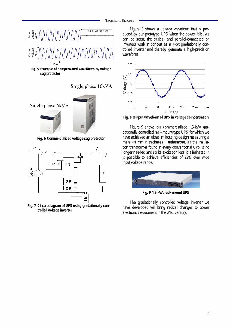
Figure 8 shows a voltage waveform that is pro-duced by our prototype UPS when the power fails. As can be seen, the series- and parallel-connected bit inverters work in concert as a 4-bit gradationally con-trolled inverter and thereby generate a high-precision waveform.
Vol
tage
(V)
Time (s) Fig. 8 Output waveform of UPS in voltage compensation
Figure 9 shows our commercialized 1.5-kVA gra-
dationally controlled rack-mount-type UPS for which we have achieved an ultraslim housing design measuring a mere 44 mm in thickness. Furthermore, as the insula-tion transformer found in every conventional UPS is no longer needed and so its excitation loss is eliminated, it is possible to achieve efficiencies of 95% over wide input voltage range.
Fig. 9 1.5-kVA rack-mount UPS
The gradationally controlled voltage inverter we
have developed will bring radical changes to power electronics equipment in the 21st century.
8

TECHNICAL REPORTS
Electromagnetic Noises from Power Devices and Filter Design
Authors: Akinori Nishizawa* and Satoshi Azuma*
1. Introduction
Technologies for designing power electronic cir-cuits which are used in everything from industrial and communications equipment to household electrical appliances are an important factor that determines the quality and cost of such products. In recent years, regulations concerning electromagnetic noise (emis-sions) have been tightened. It has become necessary to obtain the CE marking based on the recommenda-tions of CISPR (Comite international Special des Per-turbations Radioelectriques) and other institutions in Europe as well as certification from the FCC (Federal Communications Commission) in North America in order to export products to those regions. Regulations are also being tightened in the Japanese domestic market.
Under these circumstances, technologies for de-termining filter configurations and the like at the design stage by simulating the noise generated by power electronic circuitry have been growing in importance(3) in order to raise the reliability of products yet reduce their cost. Regarding noise filtering technologies, pro-gress is being made in studies of active filters(4), which are configured to generate voltage of opposite phase to cancel out noise, in addition to conventional pas-sive-type filters.
2. Simulation of electromagnetic noise 2.1 Modeling of electromagnetic noise sources
The electromagnetic noise generated in power electronic circuits such as inverters is caused by the high-speed switching operation of transistors and free-wheeling diodes that are found in those circuits. As an example, a 600V/150A IGBT (insulated-gate bipolar transistor) module's turn-on and turn-off waveforms are shown in Fig. 1.
As for the switching operation of recent IGBTs, voltage rise and fall times are on the order of 100 nsec. This means that noise cannot be reduced even by reducing the speed of switching operation, and so noise filter-based measures must be used. On the other hand, where radiated emissions are concerned, since oscilla-tion at the time of reverse recovery of freewheeling diodes can be suppressed by an increase in transis-tor-driving gate resistance, the radiated emissions are expected to be reduced at the expense of an increase
in loss associated with switching. The modeling of such an electromagnetic noise source is important when making predictions about electromagnetic noise in the design stage. Therefore, an analytical model is needed that reflects the features of generating factors for con-ducted and radiated emissions.
(a) Turnn on
(b) Turn off
Fig. 1 Waveforms of IGBT switching
2.2 Analysis of conducted emissions EMI (electromagnetic interference) emission in in-
verter equipment is caused by the switching operation of the equipment’s power devices. Carrier frequencies are usually on the order of 10 kHz. Taking a look at various EMI standards, regulations on conducted EMI emissions often begin at 150 kHz, so conducted EMI emissions in the neighborhood of 150 kHz should be focused on. Since this 150-kHz band is home to the lower-order harmonics of inverter carrier frequencies, this is where Fourier harmonic components of switching carriers come into direct view and where conducted emissions (noise voltage across terminals) occur with
*Advanced Technology R&D Center Mitsubishi Electric ADVANCE March 2006 9
TECHNICAL REPORTS
uipment who
d emissions in a cir-cuit
the greatest magnitude. In order to suppress conducted emissions in this band, a noise filter is usually installed. Also, for determining filter specifications, the amount of emissions in this band needs to be estimated.
Here, we will consider an inverter eqse load is a motor. As for a typical setup for meas-
uring conducted emissions from inverter equipment, the AC line power is connected to the inverter equipment by an LISN (Line Impedance Stabilization Network) (and then through a noise filter) while the load (motor in this case) is connected to the inverter equipment through an output cable. By feeding the output of the LISN into a spectrum analyzer or the like, it is possible to measure conducted emissions.
In order to compute conductesimulation, it is necessary to prepare an equivalent
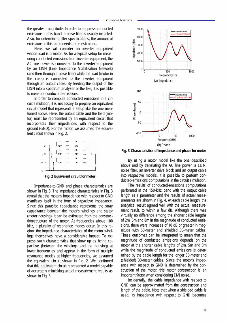
circuit model that represents a setup like the one men-tioned above. Here, the output cable and the load (mo-tor) must be represented by an equivalent circuit that incorporates their impedances with respect to the ground (GND). For the motor, we assumed the equiva-lent circuit shown in Fig. 2.
U
V
W
E Fig. 2 Equivalent circuit for motor
pedance-to-GND and phase characteristics are
showImn in Fig. 3. The impedance characteristics in Fig. 3
reveal that the motor's impedance with respect to GND manifests itself in the form of capacitive impedance. Since this parasitic capacitance represents the stray capacitance between the motor's windings and stator (motor housing), it can be estimated from the construc-tion/structure of the motor. At frequencies above 100 kHz, a plurality of resonance modes occur. In this re-gion, the impedance characteristics of the motor wind-ings themselves have a considerable impact. To ex-press such characteristics that show up as being ca-pacitive (between the windings and the housing) at lower frequencies and appear in the form of multiple resonance modes at higher frequencies, we assumed the equivalent circuit shown in Fig. 2. We confirmed that this equivalent circuit represented a model capable of accurately mimicking actual measurement results as shown in Fig. 3.
0
1000
2000
3000
4000
5000
10 100 1000
Mesurements Equivalent Circuit
Impe
danc
e (oh
m)
Frequency(kHz) (a) Impedance
-100
-50
0
50
100
1 10 100 1000
MesurementsEquivalent Circuit
Phas
e(de
gree
)Frequency(kHz)
(b) Phase
Fig. 3 Characteristics of impedance and phase for motor By using a motor model like the one described
above and by translating the AC line power, a LISN, noise filter, an inverter drive block and an output cable into respective models, it is possible to perform con-ducted-emissions computations in the circuit simulation.
The results of conducted-emissions computations performed in the 150-kHz band with the output cable length as a parameter and the results of actual meas-urements are shown in Fig. 4. At each cable length, the analytical result agreed well with the actual measure-ment result, to within a few dB. Although there was virtually no difference among the shorter cable lengths of 2m, 5m and 8m in the magnitude of conducted emis-sions, there were increases of 10 dB or greater in mag-nitude with 50-meter and shielded 30-meter cables. These outcomes can be interpreted to mean that the magnitude of conducted emissions depends on the motor at the shorter cable lengths of 2m, 5m and 8m while the magnitude of conducted emissions is deter-mined by the cable length for the longer 50-meter and (shielded) 30-meter cables. Since the motor's imped-ance with respect to GND is determined by the con-struction of the motor, this motor construction is an important factor when considering EMI noise.
Incidentally, the cable impedance with respect to GND can be approximated from the construction and length of the cable. Note that when a shielded cable is used, its impedance with respect to GND becomes
10
TECHNICAL REPORTS
smaller because of its shielding metal, and conducted emissions become greater in magnitude when com-pared with its unshielded counterpart. As has been discussed, since the magnitude of conducted emissions depends on the impedances of the inverter equipment's cable and load with respect to GND, it is necessary to consider the impedances of the cable and load with respect to GND. This will enable conducted emissions of particular inverter equipment to be calculated. Based on the results of the calculations, it then becomes pos-sible to design noise filters to keep EMI within specifica-tion and also to estimate the impact of extending the cable length.
10
20
30
40
50
60
70
2m 5m 8m 50m 30m
Measurements Computed results
Cond
ucted
emiss
ion(d
B)
Cable length(m) (Shielded)
Fig. 4 Conducted emission for cable length 3. Designing noise filters 3.1 Passive noise filters
For inverter equipment, noise filters are virtually in-dispensable in view of the EMI standards. Passive-type noise filters are generally made up of common-mode coils, capacitors to be connected to GND, and capaci-tors to be placed across phases. The amount of fil-ter-induced attenuation is determined by the character-istics of those components. While a filter is still at the design stage, it is natural to theoretically secure the desired amount of attenuation. However, this alone does not suffice and it is necessary to pay attention to (1) installation positions, (2) magnetic saturation of coil cores, (3) leakage current, and the like.
When a common-mode coil, which is made by winding a large number of turns onto a small core, is used, the core can go into magnetic saturation. There-fore, it is necessary to estimate the magnitude of com-mon-mode current that can occur and decide upon a core size and the number of winding turns so as to avoid saturation. Furthermore, since such a noise filter is made up of LC circuitry, it has a resonant frequency. If this resonant frequency coincides with a carrier fre-quency, a high common-mode current will be produced, so care is required. Moreover, regarding the magnetic fluxes produced by coil cores, often only those fluxes that are generated by common-mode current are con-sidered. However, magnetic flux is also generated by
normal-mode (commercial frequency) current on ac-count of leakage inductance. Since the normal mode has a large current value, for the flux that will develop in the coil core, it is necessary to predict the saturation strength based on the flux amount determined by com-bining common-mode-induced flux and nor-mal-mode-induced flux.
There is also another means by which capacitance with respect to GND is increased in order to provide added attenuation. However, since augmenting the capacitance increases low-frequency leakage current, it is necessary to decide the capacitor capacitance with a sufficient allowance to avoid problems by considering the configuration of a given commercial power supply. Furthermore, the leakage current is greatly impacted by the impedance of the load (for example, motor) with respect to GND in addition to the capacitance with respect to GND. Caution is required because, when a load having a small impedance (or a large parasitic capacitance) is installed, the load will give rise to a greater leakage current than ground-connected ca-pacitors would do.
3.2 Active noise filters
A typical technique for reducing electromagnetic noise is to connect a passive filter, but this inevitably increases the overall volume and cost of a given in-verter system. There are also problems of resonance that occurs between reactors and capacitors making up a passive filter as well as magnetic saturation in the cores of such reactors. Therefore, we propose “active noise filtering” that is characterized by its ability to reduce both normal-mode and common-mode con-ducted emissions, eliminates the need for a com-mon-mode transformer, and makes it possible to re-duce the breakdown voltage of transistors that are active elements (meaning that transistors with lower breakdown voltages may be used). An active noise filter is designed to directly detect conducted emissions and perform feedback control on output current for each individual phase with the help of transistor circuitry so as to reduce those conducted emissions to zero. Figure 5 shows a per-phase block diagram of an active noise filter, where CNV, INV and IM represent a rectifier, an inverter and an induction motor, respectively. Here, high-frequency voltage vcy that appears across para-sitic capacitance Cy existing along an AC line cable and the like corresponds to conducted emissions observed by an LISN. Therefore, to suppress this high-frequency voltage vcy, the active filter has the following functions:
Detection of voltage vcy across Cy Extraction of high-frequency voltage components
(150 kHz and above, for example) by the high-pass filter (HPF) as conducted emissions to be sup-pressed
Mitsubishi Electric ADVANCE March 2006 11
TECHNICAL REPORTS
Creation of current command icom* with proportional gain K so that the above high-frequency voltage components become zero
Conversion of voltage signal icom* to current icom by means of ±15V-powered voltage-to-current conver-sion circuitry (V-to-I Conv.) and injection of icom into Cy through capacitor Cin.
Fig. 5 Block diagram of active noise filter
The results of conductive-emissions measure-
ments performed on an inverter in operation with the help of an LISN are shown in Fig. 6. Since the AC line power used represents a 3-phase input, we connected the per-phase functional block shown in Fig. 5 to each of the three phases. The active noise filter provided an attenuation of approximately 20 dB in the neighborhood of 150 kHz as intended by its design which we devel-oped using a Bode diagram. For conducted emissions in MHz bands, they can be reduced by connecting separate phase-to-phase capacitors. We have started making verification studies of optimum designs, each employing active noise filtering and simple passive noise filtering.
[Hz]
dBµ[V]
Without active noise filter
With active noise filter
Fig. 6 Measurements of conducted emission
4. Conclusion In this paper, we have discussed our technologies
for embodying power electronics circuitry and noise (emission) propagation into models and design noise filters. By building everything, from the inverter circuit and cable to the motor that acts as a load, into an equivalent circuit model, it becomes possible to make quantitative EMI-emissions assessments of arbitrary combinations of those models. Thanks to these tech-nologies, it has now become possible to select filter constants and create a design from the drawing stage, thus shortening development times and reducing cost. We are also forging ahead with the commercialization of a more adaptive filtering technology like the one embodied in active filters. References (1) R. Rohrer, L. Nagel, R. Meyer and L. Weber,
“Computationally efficient electronic-circuit noise calculations,” IEEE Journal of Solid-State Circuits, Vol. SC-6, No. 4, 1971
(2) L. Nagel, “SPICE2: A Computer Program to Simu-late Semiconductor Circuits,” Ph.D. dissertation, University of California at Berkeley, 1975.
(3) A. Nishizawa, S. Tanabe and M. Nakanishi, “Switching interference from power electron-ics-applied devices”, J. IEIE Jpn. Vol. 24, No. 4, pp. 275-278, 2004
(4) S. Azuma and M. Kimata, “Active noise filter to reduce normal-mode and common-mode con-ducted EMI noise”, IEEJ Trans. IA, Vol. 124, No. 9, pp. 893-900, 2004
12
TECHNICAL REPORTS
Evaluation of Fatigue Life Reliability and New Lead Bonding Technology
for Power Modules Authors: Toshihiro Matsunaga* and Shingo Sudo**
The authors have developed a fast thermal cycling test method of evaluating the reliability of power mod-ules. The method shortens the time required for a life evaluation test of Al wire bond lift-off to one-quarter of the conventional power cycling test method. The au-thors have also developed a technology for Cu lead interconnection structures that can be applied for higher current densities of chips and improved productivity, replacing the current Al wiring method.
1. Introduction
Power modules, which are used for an increasingly wide range of industrial applications, are used not only for inverter control of household electric appliances but also for high power applications that include automo-biles, electric railroads, and electric power. Today’s power modules require far greater reliability with re-spect to electric performance, insulation efficiency, thermal performance, and strength, and so it is ex-pected that the specifications of such modules will improve. It has also become necessary to rapidly de-velop and commercialize products of low cost and high reliability. To meet these requirements, we have to improve the accuracy and speed of reliability evaluation techniques and develop products based on new tech-nological concepts.
This paper deals with two types of technology. The first one is a technology for quickly evaluating the thermal fatigue wire lift-off life of Al wire bond used for the main electrode interconnections in power modules, as a means of evaluating the strength reliability for power module wiring structures. The second technology is related to a wiring structure with thin Cu lead as a new bonding method that supersedes the conventional wire bonding method and meets the future needs for high current densities.
2. Strength Reliability Evaluation Tech-
nology (Accelerated Testing Technol-ogy for Wire Lift-off Life)
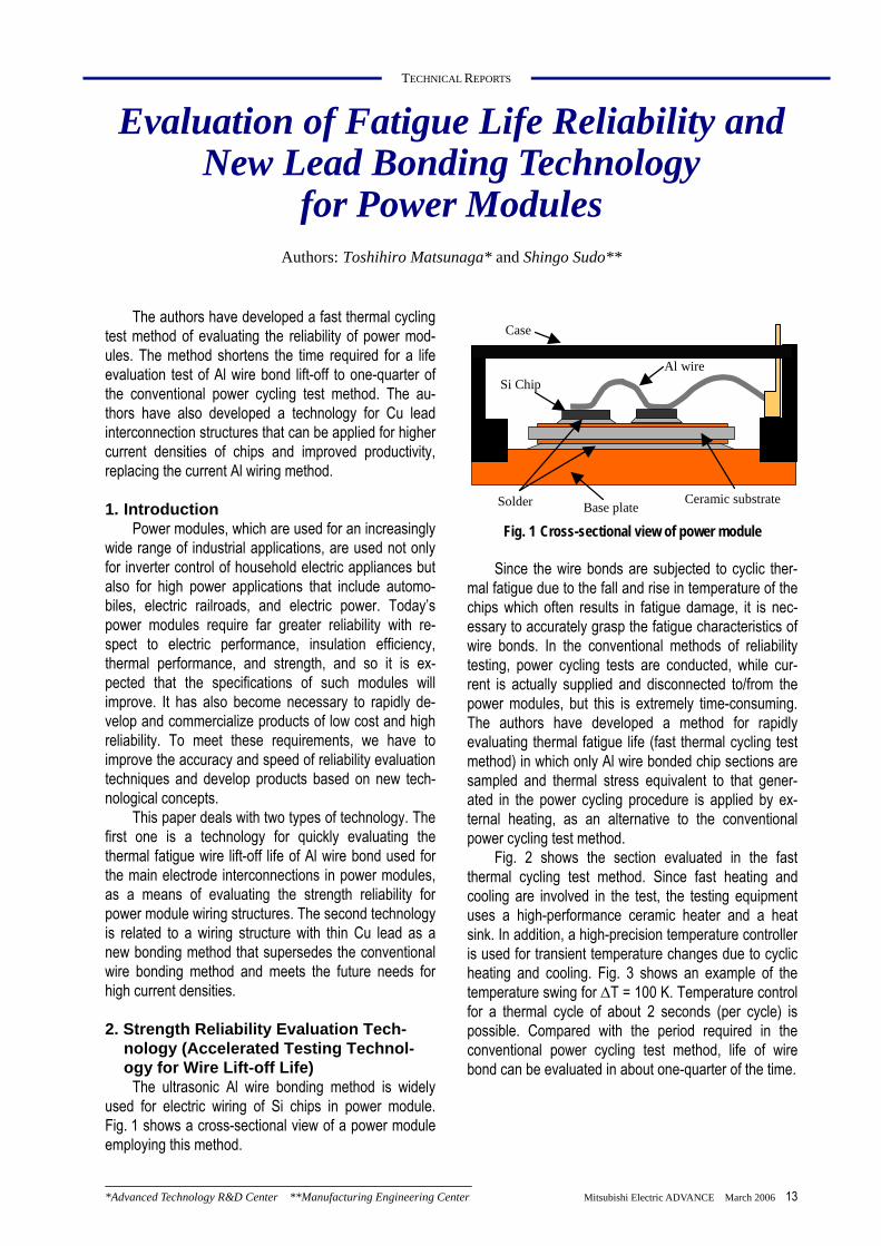
The ultrasonic Al wire bonding method is widely used for electric wiring of Si chips in power module. Fig. 1 shows a cross-sectional view of a power module employing this method.
Al wire Si Chip
Solder Ceramic substrate Base plate
Case
Fig. 1 Cross-sectional view of power module Since the wire bonds are subjected to cyclic ther-
mal fatigue due to the fall and rise in temperature of the chips which often results in fatigue damage, it is nec-essary to accurately grasp the fatigue characteristics of wire bonds. In the conventional methods of reliability testing, power cycling tests are conducted, while cur-rent is actually supplied and disconnected to/from the power modules, but this is extremely time-consuming. The authors have developed a method for rapidly evaluating thermal fatigue life (fast thermal cycling test method) in which only Al wire bonded chip sections are sampled and thermal stress equivalent to that gener-ated in the power cycling procedure is applied by ex-ternal heating, as an alternative to the conventional power cycling test method.
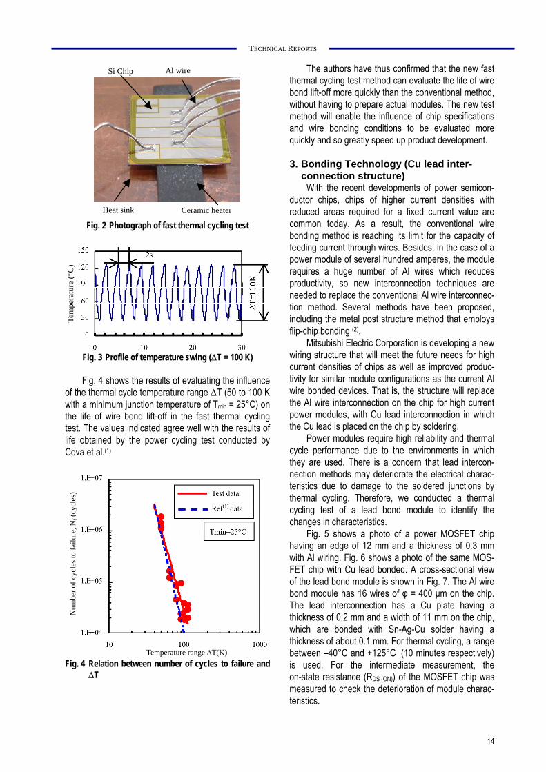
Fig. 2 shows the section evaluated in the fast thermal cycling test method. Since fast heating and cooling are involved in the test, the testing equipment uses a high-performance ceramic heater and a heat sink. In addition, a high-precision temperature controller is used for transient temperature changes due to cyclic heating and cooling. Fig. 3 shows an example of the temperature swing for ∆T = 100 K. Temperature control for a thermal cycle of about 2 seconds (per cycle) is possible. Compared with the period required in the conventional power cycling test method, life of wire bond can be evaluated in about one-quarter of the time.
*Advanced Technology R&D Center **Manufacturing Engineering Center Mitsubishi Electric ADVANCE March 2006 13
TECHNICAL REPORTS
Al wire
Ceramic heater
Si Chip
Heat sink Fig. 2 Photograph of fast thermal cycling test
Tem
pera
ture
(°C
)
Fig. 3 Profile of temperature swing (∆T = 100 K) Fig. 4 shows the results of evaluating the influence
of the thermal cycle temperature range ∆T (50 to 100 K with a minimum junction temperature of Tmin = 25°C) on the life of wire bond lift-off in the fast thermal cycling test. The values indicated agree well with the results of life obtained by the power cycling test conducted by Cova et al.(1)
Num
ber o
f cyc
les t
o fa
ilure
, Nf (
cycl
es)
Temperature range ∆T(K) Fig. 4 Relation between number of cycles to failure and
∆T
The authors have thus confirmed that the new fast thermal cycling test method can evaluate the life of wire bond lift-off more quickly than the conventional method, without having to prepare actual modules. The new test method will enable the influence of chip specifications and wire bonding conditions to be evaluated more quickly and so greatly speed up product development.
3. Bonding Technology (Cu lead inter-
connection structure) With the recent developments of power semicon-
ductor chips, chips of higher current densities with reduced areas required for a fixed current value are common today. As a result, the conventional wire bonding method is reaching its limit for the capacity of feeding current through wires. Besides, in the case of a power module of several hundred amperes, the module requires a huge number of Al wires which reduces productivity, so new interconnection techniques are needed to replace the conventional Al wire interconnec-tion method. Several methods have been proposed, including the metal post structure method that employs flip-chip bonding (2).
Mitsubishi Electric Corporation is developing a new wiring structure that will meet the future needs for high current densities of chips as well as improved produc-tivity for similar module configurations as the current Al wire bonded devices. That is, the structure will replace the Al wire interconnection on the chip for high current power modules, with Cu lead interconnection in which the Cu lead is placed on the chip by soldering.
Power modules require high reliability and thermal cycle performance due to the environments in which they are used. There is a concern that lead intercon-nection methods may deteriorate the electrical charac-teristics due to damage to the soldered junctions by thermal cycling. Therefore, we conducted a thermal cycling test of a lead bond module to identify the changes in characteristics.
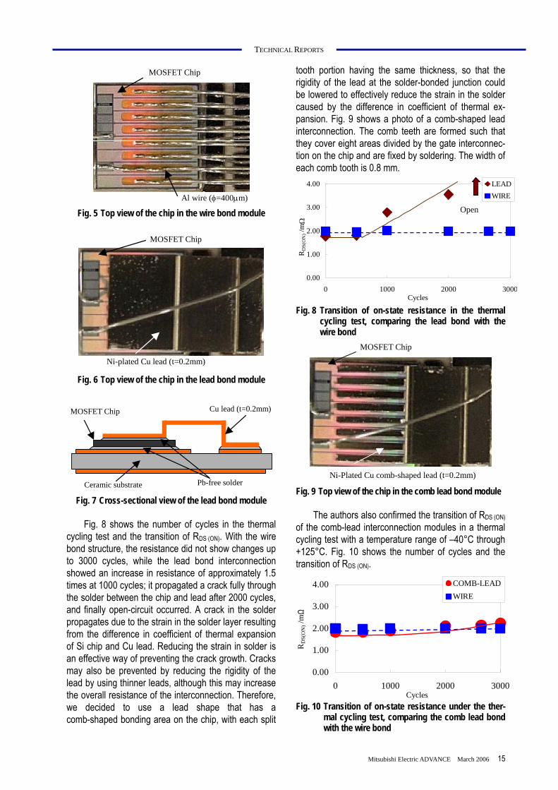
Fig. 5 shows a photo of a power MOSFET chip having an edge of 12 mm and a thickness of 0.3 mm with Al wiring. Fig. 6 shows a photo of the same MOS-FET chip with Cu lead bonded. A cross-sectional view of the lead bond module is shown in Fig. 7. The Al wire bond module has 16 wires of φ = 400 µm on the chip. The lead interconnection has a Cu plate having a thickness of 0.2 mm and a width of 11 mm on the chip, which are bonded with Sn-Ag-Cu solder having a thickness of about 0.1 mm. For thermal cycling, a range between –40°C and +125°C (10 minutes respectively) is used. For the intermediate measurement, the on-state resistance (RDS (ON)) of the MOSFET chip was measured to check the deterioration of module charac-teristics.
14
TECHNICAL REPORTS
MOSFET Chip
Al wire (φ=400µm) Fig. 5 Top view of the chip in the wire bond module
Ni-plated Cu lead (t=0.2mm)
MOSFET Chip
Fig. 6 Top view of the chip in the lead bond module
Cu lead (t=0.2mm)MOSFET Chip
Pb-free solder Ceramic substrate Fig. 7 Cross-sectional view of the lead bond module
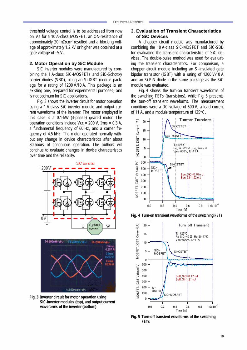
Fig. 8 shows the number of cycles in the thermal
cycling test and the transition of RDS (ON). With the wire bond structure, the resistance did not show changes up to 3000 cycles, while the lead bond interconnection showed an increase in resistance of approximately 1.5 times at 1000 cycles; it propagated a crack fully through the solder between the chip and lead after 2000 cycles, and finally open-circuit occurred. A crack in the solder propagates due to the strain in the solder layer resulting from the difference in coefficient of thermal expansion of Si chip and Cu lead. Reducing the strain in solder is an effective way of preventing the crack growth. Cracks may also be prevented by reducing the rigidity of the lead by using thinner leads, although this may increase the overall resistance of the interconnection. Therefore, we decided to use a lead shape that has a comb-shaped bonding area on the chip, with each split
tooth portion having the same thickness, so that the rigidity of the lead at the solder-bonded junction could be lowered to effectively reduce the strain in the solder caused by the difference in coefficient of thermal ex-pansion. Fig. 9 shows a photo of a comb-shaped lead interconnection. The comb teeth are formed such that they cover eight areas divided by the gate interconnec-tion on the chip and are fixed by soldering. The width of each comb tooth is 0.8 mm.
0.00
1.00
2.00
3.00
4.00
0 1000 2000 3000Cycles
RD
S(O
N) /
mΩ
LEADWIRE
Open
Fig. 8 Transition of on-state resistance in the thermal
cycling test, comparing the lead bond with the wire bond
Ni-Plated Cu comb-shaped lead (t=0.2mm)
MOSFET Chip
Fig. 9 Top view of the chip in the comb lead bond module
The authors also confirmed the transition of RDS (ON)
of the comb-lead interconnection modules in a thermal cycling test with a temperature range of –40°C through +125°C. Fig. 10 shows the number of cycles and the transition of RDS (ON).
0.00
1.00
2.00
3.00
4.00
0 1000 2000 3000Cycles
RD
S(O
N) /
mΩ
COMB-LEADWIRE
Fig. 10 Transition of on-state resistance under the ther-
mal cycling test, comparing the comb lead bond with the wire bond
Mitsubishi Electric ADVANCE March 2006 15

TECHNICAL REPORTS
The thermal cycling test clearly shows that the comb-shaped lead interconnection structure can keep the increase in RDS (ON) beyond 1000 cycles. Further-more, the structure does not suffer an open-circuit at 3000 cycles, with the increase in RDS (ON) suppressed to around 10%.
4. Conclusion
The authors have developed and confirmed the effectiveness of a fast thermal cycling test method for evaluating the life of Al wire bond lift-off more quickly than the conventional method, for evaluating the reli-ability of power modules. The authors have also pro-posed a Cu lead interconnection structure as a new interconnection method and proved that use of the comb-shaped lead divided into teeth is effective in preventing cracks in the solder used to bond the chip and lead under thermal cycling conditions.
References: (1) P. Cova and F. Fantini, “On the effect of power
cycling stress on IGBT modules”, Microelectronics Reliability 38, (1998), pp. 1347–1352.
(2) X. Liu and G. Lu, “Power Chip Interconnection: From Wire Bonding to Area Bonding”, IMAPS2000, Boston, (2000), pp. 264–269.
16

TECHNICAL REPORTS
SiC Devices and Their Application Technologies
Authors: Shin-ichi Kinouchi* and Masayuki Imaizumi*
Semiconductor silicon carbide (SiC) is expected to be the promising material for next-generation power devices. However, since crystal growth techniques and device process techniques are still immature, SiC de-vices sufficient for practical use have not yet been developed. Mitsubishi Electric Corporation has been actively developing fundamental SiC technologies, and prototypes of 10 A-class devices are now being manu-factured in order to achieve practical applications.
1. Manufacture and Electrical Static Char-
acteristics of SiC-MOSFET The size of the unit cell of the SiC-metal oxide
semiconductor field effect transistor (MOSFET) ex-perimentally manufactured this time is 25x25 µm with a gate length of 2 µm. Two types of MOSFET prototype with an active area per chip of 0.88 mm2 and 7.8 mm2 were manufactured. These are respectively equivalent to 1 A-class and 10 A-class current ratings.
Their substrates are 4H-polytype n-type SiC. A drift layer with a donor density of 1x1016 cm-3 and a thick-ness of 12 µm was prepared by epitaxial growth. The well region and JTE (junction termination extension) region were implanted with Al ions as p-type dopant and subjected to activation annealing in pres-sure-reduced Ar atmosphere. After removing the sur-face layer formed by activation annealing, an n-type
channel layer was formed by epitaxial growth. The thickness and density of this particular channel layer were set so as to ensure that the whole layer would be depleted through pn junction with the p-type well layer. The gate oxide film was formed by thermal oxidation in a steam and oxygen atmosphere. The gate electrode was poly-Si doped with P. After interlayer dielectrics were deposited, the metallic electrodes of source, drain, and gate were formed.
Fig. 1 shows typical drain current and drain voltage characteristics (ON characteristics) of the 1 A-class SiC prototype. A specific ON-resistance of 12.9 mΩcm2 resulted from a gate voltage of 12 V (field intensity in the gate oxide film: 3 MV/cm) and a current density of 50 A/cm2. For comparison with Si, the value at this particular current density is taken. Fig. 2 shows the blocking characteristics (OFF characteristics) of the MOSFET shown in Fig. 1. Although there is a leakage current from the MOS channel section at a gate voltage of 0 V, an avalanche breakdown voltage of 1.2 kV or more results. The current values remain unchanged at gate voltages lower than –5 V (due to the absence of channel leakage current). The threshold voltages of the MOSFET manufactured experimentally this time range from approximately –0.5 V to 0.5 V and tend to lower as the ON-resistance is reduced. A gate voltage lower than –5 V is necessary to surely turn the MOSFET off;
Drain voltage (V)
Dra
in c
urre
nt (A
)
Drain voltage (V)
Dra
in c
urre
nt (A
)
Fig. 1 1 A-class SiC-MOSFET drain current vs. Fig. 2 Blocking characteristics of 1 A-class
drain voltage SiC-MOSFET*Advanced Technology R&D Center Mitsubishi Electric ADVANCE March 2006 17
TECHNICAL REPORTS
threshold voltage control is to be addressed from now on. As for a 10 A-class MOSFET, an ON-resistance of approximately 20 mΩcm2 resulted and a blocking volt-age of approximately 1.2 kV or higher was obtained at a gate voltage of –5 V.
2. Motor Operation by SiC Module
SiC inverter modules were manufactured by com-bining the 1 A-class SiC-MOSFETs and SiC-Schottky barrier diodes (SBD), using an Si-IGBT module pack-age for a rating of 1200 V/10 A. This package is an existing one, prepared for experimental purposes, and is not optimum for SiC applications.
Fig. 3 shows the inverter circuit for motor operation using a 1 A-class SiC-inverter module and output cur-rent waveforms of the inverter. The motor employed in this case is a 0.1-kW (3-phase) geared motor. The operation conditions include Vcc = 200 V, Irms = 0.3 A, a fundamental frequency of 60 Hz, and a carrier fre-quency of 4.5 kHz. The motor operated normally with-out any change in device characteristics after about 80 hours of continuous operation. The authors will continue to evaluate changes in device characteristics over time and the reliability.
Fig. 3 Inverter circuit for motor operation using
SiC-inverter modules (top), and output current waveforms of the inverter (bottom)
3. Evaluation of Transient Characteristics of SiC Devices
A chopper circuit module was manufactured by combining the 10 A-class SiC-MOSFET and SiC-SBD for evaluating the transient characteristics of SiC de-vices. The double-pulse method was used for evaluat-ing the transient characteristics. For comparison, a chopper circuit module including an Si-insulated gate bipolar transistor (IGBT) with a rating of 1200 V/10 A and an Si-PiN diode in the same package as the SiC module was evaluated.
Fig. 4 shows the turn-on transient waveforms of the switching FETs (transistors), while Fig. 5 presents the turn-off transient waveforms. The measurement conditions were a DC voltage of 600 V, a load current of 11 A, and a module temperature of 125°C.
Fig. 4 Turn-on transient waveforms of the switching FETs
20
15
10
5
0
MO
SFET, IG
BT C
urr
ent[
A]
1.0x10⁻⁶
0.80.60.40.20.0Time [s]
600
500
400
300
200
100
0MO
SFET, IG
BT V
oltag
e[V
]
Turn-off Transient
Tj=125Rg_SiC=47Ω, Rg_Si=47ΩVpn=600V, IL=11A
Eoff_SiC=0.17mJ Eoff_Si=1.21mJ
Si-CSTBT
Si-CSTBT
SiC-MOSFET
SiC-MOSFET
Fig. 5 Turn-off transient waveforms of the switching
FETs
18
TECHNICAL REPORTS
For the comparison of the turn-on waveforms be-tween SiC-MOSFET and Si-IGBT, gate resistances that result in the same turn-on di/dt with both Si module and SiC module were used. For the comparison of the turn-off waveforms between SiC-MOSFET and Si-IGBT, a gate resistance that results in the same surge voltage with both Si module and SiC module was used. The gate resistance used in turn-on was 20 Ω with the SiC-MOSFET and 47 Ω with the Si-IGBT. On the other hand, the gate resistance used in turn-off was 47 Ω with the SiC-MOSFET and 47 Ω with the Si-IGBT.
Fig. 4 clearly indicates that the difference in the reverse recovery behavior of the diodes had a great influence on the turn-on loss. Recovery current slightly higher than 2 A due to the extension of the depleted region of SiC-SBD is observed in the SiC module, but it is far lower than the recovery current of the Si-PiN diode. Fig. 5 shows clearly that there is a big difference in the tail current values of the switching transistors. Since the SiC-MOSFET is a unipolar device, no carrier storage is present at the turn-off moment and no tail current is generated in principle.
Comparison of the transient loss between the SiC module and Si-IGBT module under the measurement conditions mentioned above reveals that the turn-off loss of the SiC module is 0.60 times that of the Si mod-ule, the turn-on loss is 0.14 times, and the diode recov-ery loss is 0.02 times.
4. Trial Calculation of Inverter Operation Loss
Based on the transient characteristics and static characteristics of the SiC devices used in this study, the loss during the operation of the 3-phase pulse width modulation (PWM) inverter was calculated. The condi-tions used in the loss calculation include a module temperature of 125°C, a DC voltage of 600 V, a phase current of Irms = 3.5 A, a carrier frequency of 10 kHz, a PWM modulation ratio of 1.0, and a power factor of 0.8. Comparing the SiC inverter with the Si inverter, the transient loss (turn-on + turn-off + recovery) of the SiC inverter was reduced to 23% that of the Si inverter, proving that the total loss of the inverter can be reduced to 44%.
We will continue to improve the performance and reliability of SiC-MOSFETs and SiC-SBDs with a view to using SiC modules in practical applications.
Part of this study was conducted under a joint re-search contract with the New Energy and Industrial Technology Development Organization (NEDO) as one of the “Strategic Development of Technology for Effi-cient Energy Utilization” financed by a subsidy from the Ministry of Economy, Trade and Industry.
Mitsubishi Electric ADVANCE March 2006 19
TECHNICAL REPORTS
Technologies of Power Electronics for Air Conditioner and
Household Electric Appliances Authors: Mamoru Kawakubo* and Masaaki Yabe*
Household electric appliances such as air condi-tioners and refrigerators are commonly equipped with inverters that make extensive use of power electronics technologies. The power electronics technologies de-veloped for conserving energy and resources have helped greatly reduce power consumption as well as the amount of materials used for construction. This paper reviews the technologies used to improve the operation efficiency and resource saving effects of brushless DC motors and the inverters to dive the motors.
1. Technologies for Improving Efficiency
of Inverters Used in Compressors The inverters installed in air conditioners or refrig-
erators efficiently drive brushless DC motors for com-pressors. The environment within compressors is sub-ject to high temperature and high pressure conditions and it is very difficult to install position sensors for de-tecting the magnetic poles of rotors inside. In other words, a position-sensorless driving method is essential. The conventional brushless DC motors are driven by rectangular-wave inverters for ease of control, but the many harmonics contained in the motor current cause iron loss or great torque ripple. To solve this problem, we have developed a sine-wave inverter and installed it in air conditioners, refrigerators, and other electric appliances.
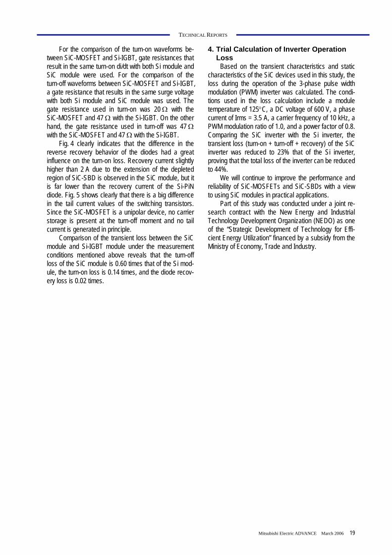
The inverter is installed in a vector control feature and the motor is driven synchronously. Fig. 1 shows the control block diagram. This control method employing a frequency compensator maintains stable rotational speed in spite of fluctuations in load torque of the motor, thus reducing the arithmetic load for control.
The inverter is required to drive the compressor motor over a wide range of speed, from low speed to high speed, and must drive the motor very efficiently particularly in the middle- and low-speed ranges where the duration of operation is long. To meet this require-ment, we have developed an over-modulation system to drive the motor efficiently. Over-modulation PWM (Pulse Width Modulation) can increase the first har-monic output voltage since it can control part of the PWM 100% duty. With the output voltage increased by up to approximately 10%, it is possible to drive high-voltage type motors, which can be designed for lower motor current levels than low-voltage type motors. Consequently, the copper loss of the motor and iron loss of the switching device are reduced, thus improv-ing the efficiency of the motor and the inverter.
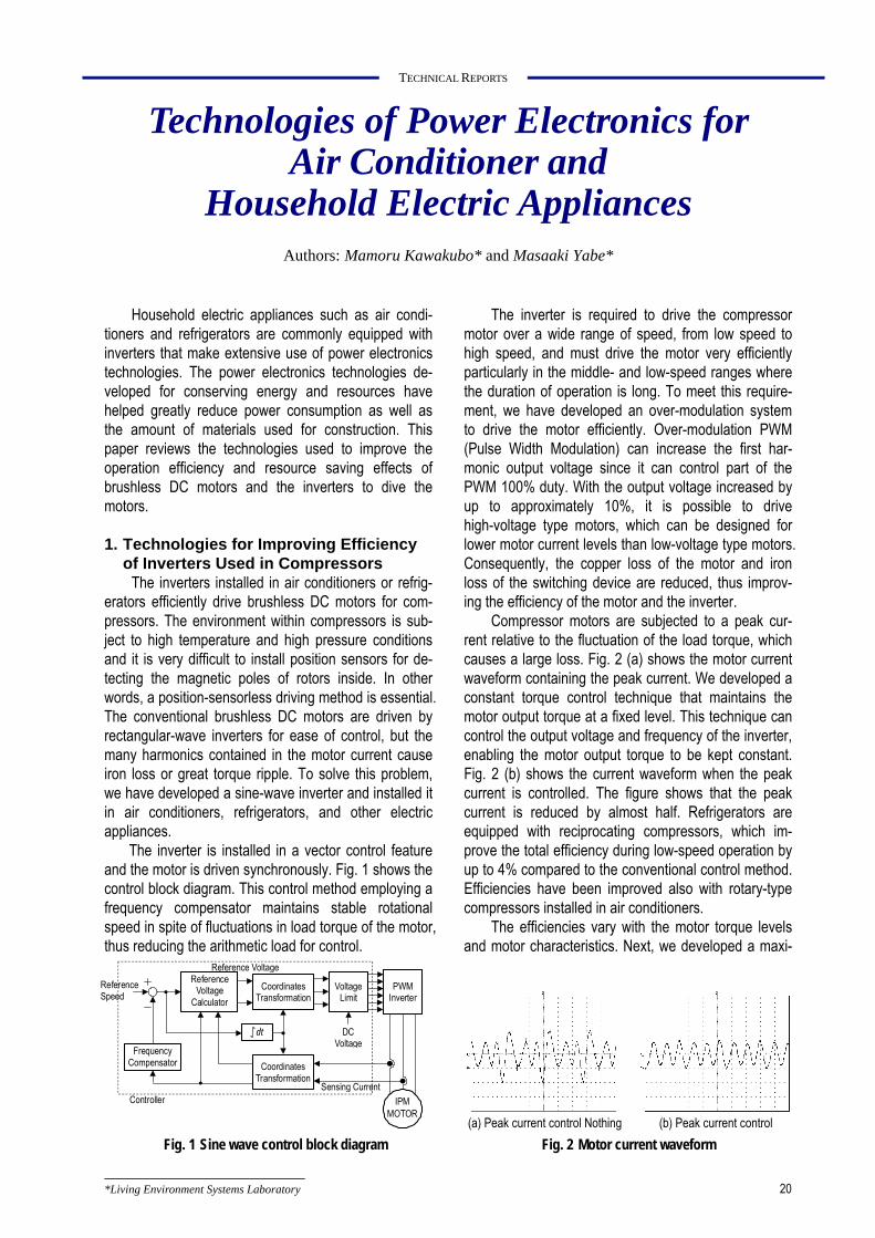
Compressor motors are subjected to a peak cur-rent relative to the fluctuation of the load torque, which causes a large loss. Fig. 2 (a) shows the motor current waveform containing the peak current. We developed a constant torque control technique that maintains the motor output torque at a fixed level. This technique can control the output voltage and frequency of the inverter, enabling the motor output torque to be kept constant. Fig. 2 (b) shows the current waveform when the peak current is controlled. The figure shows that the peak current is reduced by almost half. Refrigerators are equipped with reciprocating compressors, which im-prove the total efficiency during low-speed operation by up to 4% compared to the conventional control method. Efficiencies have been improved also with rotary-type compressors installed in air conditioners.
The efficiencies vary with the motor torque levels and motor characteristics. Next, we developed a maxi-
Reference Speed
Reference Voltage
Calculator Coordinates
Transformation
dt
Voltage Limit
PWM Inverter
DC Voltage
IPM MOTOR
Frequency Compensator Coordinates
Transformation
Controller Sensing Current
Reference Voltage
(a) Peak current control Nothing (b) Peak current control Fig. 1 Sine wave control block diagram Fig. 2 Motor current waveform
*Living Environment Systems Laboratory 20
TECHNICAL REPORTS
mum efficiency control technique for efficiently operat-ing motors of different torque levels and characteristics. This technique controls the inverter output voltage to minimize the current on the basis of the motor current value and motor parameters. With this control tech-nique, the motor efficiency of packaged air conditioners during low-speed operation is increased by up to 6%.
2. Technologies for Improving Efficiency
of Brushless DC Motors Used in Com-pressors
It is necessary to reduce copper loss and iron loss and downsize the brushless DC motors in order to improve their operation efficiency and conserve re-sources. Basically, brushless DC motors are equipped with interior permanent magnet (IPM) type rotors housed inside the rotors for their performance and manufacturing specifications. The motor torque of a brushless DC motor is given by Equation (1) below. The first term on the right of the equation represents the magnet torque, while the second term indicates the reluctance torque.
( ) qdqdqfmm iiLLiPT ⋅⋅−+⋅Φ= ................(1)
where, Tm = motor torque, id = d-axis component of
motor current, iq = q-axis component of motor current, Ld: d-axis inductance, Lq = q-axis inductance, φf = magnetic flux linkage, and Pm = pole pairs.
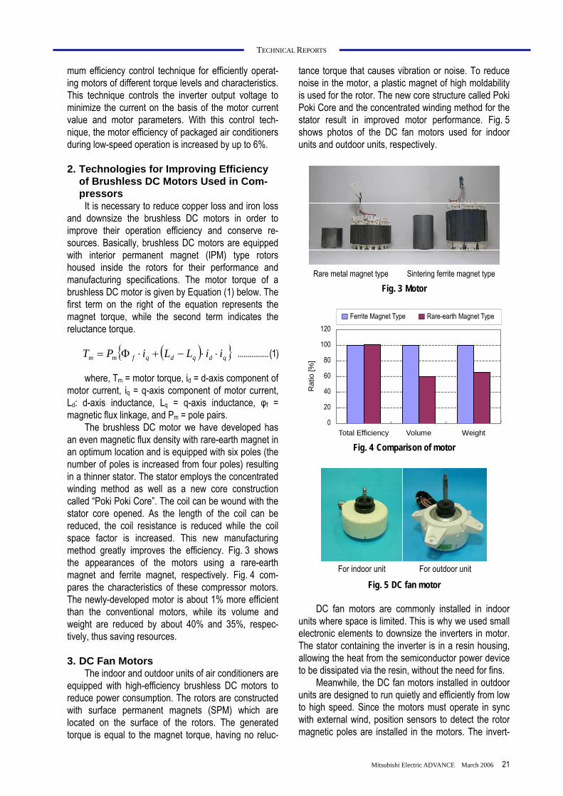
The brushless DC motor we have developed has an even magnetic flux density with rare-earth magnet in an optimum location and is equipped with six poles (the number of poles is increased from four poles) resulting in a thinner stator. The stator employs the concentrated winding method as well as a new core construction called “Poki Poki Core”. The coil can be wound with the stator core opened. As the length of the coil can be reduced, the coil resistance is reduced while the coil space factor is increased. This new manufacturing method greatly improves the efficiency. Fig. 3 shows the appearances of the motors using a rare-earth magnet and ferrite magnet, respectively. Fig. 4 com-pares the characteristics of these compressor motors. The newly-developed motor is about 1% more efficient than the conventional motors, while its volume and weight are reduced by about 40% and 35%, respec-tively, thus saving resources.
3. DC Fan Motors
The indoor and outdoor units of air conditioners are equipped with high-efficiency brushless DC motors to reduce power consumption. The rotors are constructed with surface permanent magnets (SPM) which are located on the surface of the rotors. The generated torque is equal to the magnet torque, having no reluc-
tance torque that causes vibration or noise. To reduce noise in the motor, a plastic magnet of high moldability is used for the rotor. The new core structure called Poki Poki Core and the concentrated winding method for the stator result in improved motor performance. Fig. 5 shows photos of the DC fan motors used for indoor units and outdoor units, respectively.
Rare metal magnet type Sintering ferrite magnet type Fig. 3 Motor
120
Total Efficiency
Rat
io [%
]
100
80
60
40
20
0Volume Weight
Ferrite Magnet Type Rare-earth Magnet Type
Fig. 4 Comparison of motor
For indoor unit For outdoor unit
Fig. 5 DC fan motor DC fan motors are commonly installed in indoor
units where space is limited. This is why we used small electronic elements to downsize the inverters in motor. The stator containing the inverter is in a resin housing, allowing the heat from the semiconductor power device to be dissipated via the resin, without the need for fins.
Meanwhile, the DC fan motors installed in outdoor units are designed to run quietly and efficiently from low to high speed. Since the motors must operate in sync with external wind, position sensors to detect the rotor magnetic poles are installed in the motors. The invert-
Mitsubishi Electric ADVANCE March 2006 21

TECHNICAL REPORTS
ers operate the motors in accordance with the output signals from the position sensors for optimum control of the timing of voltage application at every rotation.
The techniques for improving efficiency and down-sizing compressor and DC fan motors and inverters can be applied to other electric appliances. Demand for conserving energy and resources in air conditioners and household electric appliances is very high, so we intend to continue our development efforts to meet such needs.
22


![[HAVC] Fotografia: Hiroshi Sugimoto](https://img.pdfslide.tips/doc/110x75/558cde7dd8b42a155a8b4614/havc-fotografia-hiroshi-sugimoto.jpg)