Embed Size (px)
Citation preview
Power SupplyTechnical Guide 2010/11
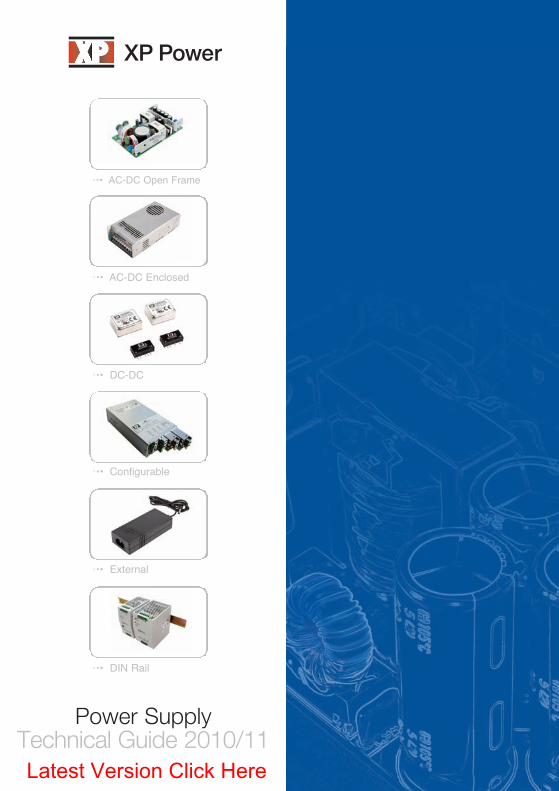
••• AC-DC Open Frame
••• AC-DC Enclosed
••• DC-DC
••• Configurable
••• External
••• DIN Rail
Latest Version Click Here

Our missionWe are committed to providing the best technical and commercialsolution for your power needs.
••• Exclusive focus on power conversion
••• Worldwide sales in excess of $100 million
••• Local engineering and sales support
••• London Stock Exchange listed
••• ISO9001 certified quality management system
••• Global commitment to the environment
To inspire our people tobe The Experts in Powerdelivering genuine valueto our customers.
Global Power Solutions
XP POWERPower Supply Technical Guide
Having trouble keeping up with the latest standards for external powersupplies such as the California Energy Commission’s (CEC) requirements forefficiency and no-load power consumption; or the implications of the 3rdEdition 60601 on Medical Safety?
Ever wondered why seemingly similar power supplies have significantlydifferent performance and reliability characteristics?
The answers to these and many more questions can be found in this, thethird edition of XP’s Power Supply Technical Guide, the culmination of many,many years experience gained by the XP Power applications team spreadover three continents.
Whether you’re new to designing-in a power supply or DC-DC converter oran ‘old hand’, this book offers an invaluable resource and all the informationyou’ll need in one easy reference guide.
We hope you find it useful, and don’t miss the five new Technology Editorialstowards the back of the guide.
i
Contents_pages_170210.qxp:Layout 1 21/6/10 09:31 Page i
ii
Introduction to Power Conversion 1
• Introduction . . . . . . . . . . . . . . . . . . . . . . . . . . . . . . . . . . . . . . . . . . . . . . . . . . . . . . . . . . . . . . . . . . 1• Switch Mode Power Supplies . . . . . . . . . . . . . . . . . . . . . . . . . . . . . . . . . . . . . . . . . . . . . . . . . . . . 1• Topologies. . . . . . . . . . . . . . . . . . . . . . . . . . . . . . . . . . . . . . . . . . . . . . . . . . . . . . . . . . . . . . . . . . . 2
Isolated Fly-back Converter. . . . . . . . . . . . . . . . . . . . . . . . . . . . . . . . . . . . . . . . . . . . . . . . 2Forward Converter . . . . . . . . . . . . . . . . . . . . . . . . . . . . . . . . . . . . . . . . . . . . . . . . . . . . . . 3Two Transistor Forward Converter . . . . . . . . . . . . . . . . . . . . . . . . . . . . . . . . . . . . . . . . . . 4Half Bridge & Full Bridge Converters . . . . . . . . . . . . . . . . . . . . . . . . . . . . . . . . . . . . . . . 5-6Push-Pull Converter . . . . . . . . . . . . . . . . . . . . . . . . . . . . . . . . . . . . . . . . . . . . . . . . . . . . . 7Buck Converter . . . . . . . . . . . . . . . . . . . . . . . . . . . . . . . . . . . . . . . . . . . . . . . . . . . . . . . . 8Boost Converter . . . . . . . . . . . . . . . . . . . . . . . . . . . . . . . . . . . . . . . . . . . . . . . . . . . . . . . . 9
• Linear Power Supplies . . . . . . . . . . . . . . . . . . . . . . . . . . . . . . . . . . . . . . . . . . . . . . . . . . . . . . . . . 10• Distributed Power Architectures . . . . . . . . . . . . . . . . . . . . . . . . . . . . . . . . . . . . . . . . . . . . . . . . . 11
Input Considerations 13
• Power Sources . . . . . . . . . . . . . . . . . . . . . . . . . . . . . . . . . . . . . . . . . . . . . . . . . . . . . . . . . . . . . . 13AC Power Sources . . . . . . . . . . . . . . . . . . . . . . . . . . . . . . . . . . . . . . . . . . . . . . . . . . . . . 13AC Generator . . . . . . . . . . . . . . . . . . . . . . . . . . . . . . . . . . . . . . . . . . . . . . . . . . . . . . . . . 13Three-phase AC . . . . . . . . . . . . . . . . . . . . . . . . . . . . . . . . . . . . . . . . . . . . . . . . . . . . . . . 15Worldwide Voltages & Frequencies . . . . . . . . . . . . . . . . . . . . . . . . . . . . . . . . . . . . . . . . . 17DC Power Sources . . . . . . . . . . . . . . . . . . . . . . . . . . . . . . . . . . . . . . . . . . . . . . . . . . . . . 18Batteries . . . . . . . . . . . . . . . . . . . . . . . . . . . . . . . . . . . . . . . . . . . . . . . . . . . . . . . . . . . . . 19
• Input Protection . . . . . . . . . . . . . . . . . . . . . . . . . . . . . . . . . . . . . . . . . . . . . . . . . . . . . . . . . . . . . . 22• AC Input Current & Harmonics . . . . . . . . . . . . . . . . . . . . . . . . . . . . . . . . . . . . . . . . . . . . . . . . . . 28• Real & Apparent Power . . . . . . . . . . . . . . . . . . . . . . . . . . . . . . . . . . . . . . . . . . . . . . . . . . . . . . . . 31• Earthing/Grounding . . . . . . . . . . . . . . . . . . . . . . . . . . . . . . . . . . . . . . . . . . . . . . . . . . . . . . . . . . . 38
DC Output Considerations 41
• Output Regulation . . . . . . . . . . . . . . . . . . . . . . . . . . . . . . . . . . . . . . . . . . . . . . . . . . . . . . . . . . . . 41• High Peak Loads . . . . . . . . . . . . . . . . . . . . . . . . . . . . . . . . . . . . . . . . . . . . . . . . . . . . . . . . . . . . . 43• Powering Light Emitting Diodes (LED’s) . . . . . . . . . . . . . . . . . . . . . . . . . . . . . . . . . . . . . . . . . . . . 45• Ripple & Noise. . . . . . . . . . . . . . . . . . . . . . . . . . . . . . . . . . . . . . . . . . . . . . . . . . . . . . . . . . . . . . . 49• Output Protection . . . . . . . . . . . . . . . . . . . . . . . . . . . . . . . . . . . . . . . . . . . . . . . . . . . . . . . . . . . . 51• Status Signals & Controls . . . . . . . . . . . . . . . . . . . . . . . . . . . . . . . . . . . . . . . . . . . . . . . . . . . . . . 55• Series & Parallel Operation. . . . . . . . . . . . . . . . . . . . . . . . . . . . . . . . . . . . . . . . . . . . . . . . . . . . . . 61• Redundant Operation . . . . . . . . . . . . . . . . . . . . . . . . . . . . . . . . . . . . . . . . . . . . . . . . . . . . . . . . . 63
Power Supply Technical Guide Contents
Contents_pages_170210.qxp:Layout 1 21/6/10 09:31 Page ii
iii
Thermal Management 64
• System Cooling Fan Selection . . . . . . . . . . . . . . . . . . . . . . . . . . . . . . . . . . . . . . . . . . . . . . . . . . . 64• Cooling Power Supplies. . . . . . . . . . . . . . . . . . . . . . . . . . . . . . . . . . . . . . . . . . . . . . . . . . . . . . . . 67• Cooling Power Modules. . . . . . . . . . . . . . . . . . . . . . . . . . . . . . . . . . . . . . . . . . . . . . . . . . . . . . . . 70• Baseplate Cooling . . . . . . . . . . . . . . . . . . . . . . . . . . . . . . . . . . . . . . . . . . . . . . . . . . . . . . . . . . . . 71
Reliability 75
• Terminology. . . . . . . . . . . . . . . . . . . . . . . . . . . . . . . . . . . . . . . . . . . . . . . . . . . . . . . . . . . . . . . . . 75• Factors Affecting Reliability . . . . . . . . . . . . . . . . . . . . . . . . . . . . . . . . . . . . . . . . . . . . . . . . . . . . . 77• System Reliability. . . . . . . . . . . . . . . . . . . . . . . . . . . . . . . . . . . . . . . . . . . . . . . . . . . . . . . . . . . . . 80
Legislation 81
• Power Supply Safety . . . . . . . . . . . . . . . . . . . . . . . . . . . . . . . . . . . . . . . . . . . . . . . . . . . . . . . . . . 81• Medical Safety . . . . . . . . . . . . . . . . . . . . . . . . . . . . . . . . . . . . . . . . . . . . . . . . . . . . . . . . . . . . . . . 84• High Voltage Safety Testing. . . . . . . . . . . . . . . . . . . . . . . . . . . . . . . . . . . . . . . . . . . . . . . . . . . . . 89• Electromagnetic Compatibility (EMC) . . . . . . . . . . . . . . . . . . . . . . . . . . . . . . . . . . . . . . . . . . . . . . 91• CE Marking . . . . . . . . . . . . . . . . . . . . . . . . . . . . . . . . . . . . . . . . . . . . . . . . . . . . . . . . . . . . . . . . . 97• Defense and Avionics EMC Standards . . . . . . . . . . . . . . . . . . . . . . . . . . . . . . . . . . . . . . . . . . . . 98• No Load Power Consumption & Efficiency Legislation for External Power Supplies. . . . . . . . . . 104• Energy Efficiency of Component Power Supplies . . . . . . . . . . . . . . . . . . . . . . . . . . . . . . . . . . . 107
Technology Editorials 109
• Technology Editorial 1. 95% High Efficiency Power Supplies. . . . . . . . . . . . . . . . . . . . . . . . . . . 109• Technology Editorial 2. Putting the Data into Power Supply Datasheets . . . . . . . . . . . . . . . . . . 115• Technology Editorial 3. Medical Power Supplies: trends, challenges & design approaches . . . . 120• Technology Editorial 4. Digital Signals and Controls . . . . . . . . . . . . . . . . . . . . . . . . . . . . . . . . . 123• Technology Editorial 5. Custom Power without Custom Pain. . . . . . . . . . . . . . . . . . . . . . . . . . 126
Further technical articles are available online at: www.xppower.com
Glossary 129
• Terms & Definitions . . . . . . . . . . . . . . . . . . . . . . . . . . . . . . . . . . . . . . . . . . . . . . . . . . . . . . . . . . 129• Prefix Codes . . . . . . . . . . . . . . . . . . . . . . . . . . . . . . . . . . . . . . . . . . . . . . . . . . . . . . . . . . . . . . . 141• SI Unit Codes . . . . . . . . . . . . . . . . . . . . . . . . . . . . . . . . . . . . . . . . . . . . . . . . . . . . . . . . . . . . . . 142
Index 143
Contents_pages_170210.qxp:Layout 1 21/6/10 09:31 Page iii
iv
© XP Power 2010Edited by Gary Bocock
Issue 3
XP POWERPower Supply Technical Guide 2010/11
Contents_pages_170210.qxp:Layout 1 21/6/10 09:31 Page iv
1
Introduction to Power Conversion
• Introduction
Electronic equipment is powered from low voltage DC supplies. The source will be either a battery, acombination of battery and DC/DC converter or a power supply converting AC mains into one ormore low voltage DC supplies. Electronic components require a DC supply that is well regulated, haslow noise characteristics and provides a fast response to load changes. AC power supplies, and mostDC/DC converters, also provide isolation from the input to the output for safety, noise reduction andtransient protection.
As electronic equipment becomes smaller and smaller, the market demands that power converters dothe same. Since the introduction of switch mode techniques, this has been an evolutionary rather thana revolutionary process. Conversion efficiency has increased, materials and components allowinghigher switching frequencies have become available and packaging techniques have advanced. At thesame time, unit cost has fallen as sales volumes have increased. With the global market a reality,power supply systems operate from wide input ranges to cover worldwide AC mains supplyvariations.
There are a number of basic topologies used in power converters, which are suited to various powerlevels, cost criteria and performance levels.
• Switch Mode Power Supplies (SMPS)
The use of switch mode topologies has reduced the size and improved the efficiency of powersupplies by increasing the frequency of operation, reducing the physical size of transformers,inductors and capacitors, and utilizing an ‘on or off’ switching element to increase efficiency. Thecompromises in adopting this technique are increased ripple and noise on the output DC supply andthe generation of both conducted and radiated EMI which have to be managed.
As switching frequency increases, so do switching losses. This has lead to the introduction ofresonant topologies, which ensure that either the voltage or the current is at zero when the switchingtransition occurs, almost eliminating these switching losses and allowing even higher operatingfrequencies. These topologies are normally referred to as Zero Voltage Switching (ZVS) or ZeroCurrent Switching (ZCS) and they have further reduced the overall volume of power supplies, orincreased power density, for a given output power.
The introduction of low voltage semiconductors and the consequent high output current demandshave driven the development of synchronous output rectifier schemes, where the output diodes arereplaced by power MOSFETs to reduce power dissipation in the secondary and achieve highefficiency solutions for these applications.
Resonant topologies and synchronous rectification are discussed in more detail in the technologyeditorials. There are a number of topologies used in switch mode converters which can be arrangedin Pulse Width Modulated (PWM), Zero Voltage Switching (ZVS), Zero Current Switching (ZCS) andsynchronous rectification schemes.
Intro_280110.qxp:Layout 1 21/6/10 09:33 Page 1
2
Introduction to Power Conversion
• Topologies
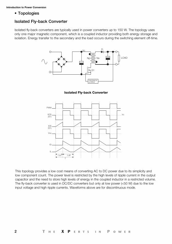
Isolated Fly-back Converter
Isolated fly-back converters are typically used in power converters up to 150 W. The topology usesonly one major magnetic component, which is a coupled inductor providing both energy storage andisolation. Energy transfer to the secondary and the load occurs during the switching element off-time.
LOAD
Vc
Np
S1
Ns
D
FEEDBACK& DRIVE
PWM
VDS(S1)
Vc
IDS(S1)
t on t offT
ID
IL
VNS
Isolated Fly-back Converter
This topology provides a low cost means of converting AC to DC power due to its simplicity andlow component count. The power level is restricted by the high levels of ripple current in the outputcapacitor and the need to store high levels of energy in the coupled inductor in a restricted volume.The fly-back converter is used in DC/DC converters but only at low power (<50 W) due to the lowinput voltage and high ripple currents. Waveforms above are for discontinuous mode.
Intro_280110.qxp:Layout 1 21/6/10 09:33 Page 2
3
Introduction to Power Conversion
LOAD
Vc D1
Np Ns
S1
D2
L
FEEDBACK & DRIVE
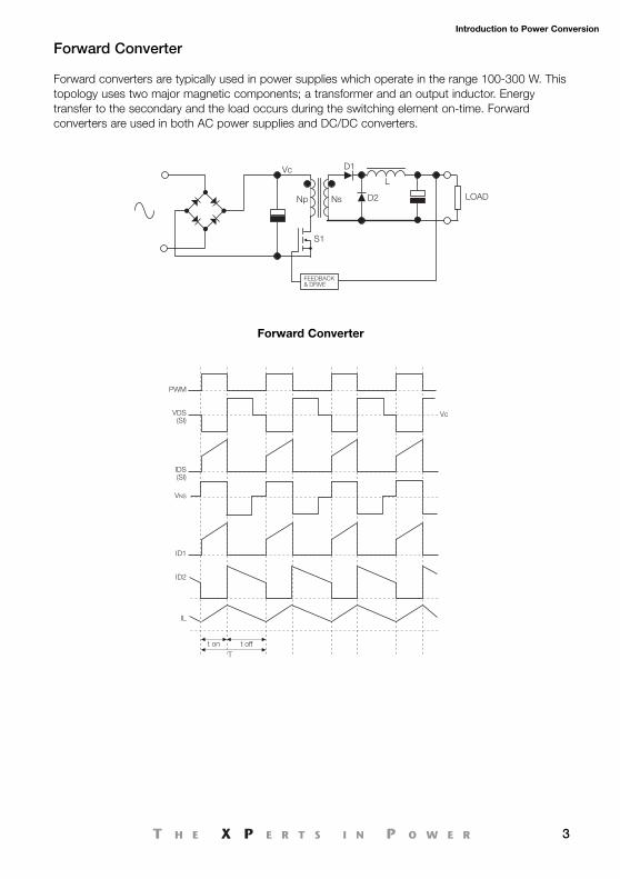
Forward Converter
Forward converters are typically used in power supplies which operate in the range 100-300 W. Thistopology uses two major magnetic components; a transformer and an output inductor. Energytransfer to the secondary and the load occurs during the switching element on-time. Forwardconverters are used in both AC power supplies and DC/DC converters.
PWM
VDS(SI)
Vc
IDS(SI)
VNS
ID1
ID2
t on t offT
IL
Forward Converter
Intro_280110.qxp:Layout 1 21/6/10 09:33 Page 3
4
Introduction to Power Conversion
Two Transistor Forward Converter
LOAD
Vc
Np Ns D2
S2D1 L
S1
FEEDBACK & DRIVE
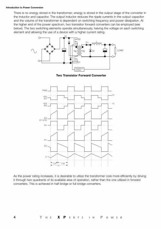
There is no energy stored in the transformer; energy is stored in the output stage of the converter inthe inductor and capacitor. The output inductor reduces the ripple currents in the output capacitorand the volume of the transformer is dependent on switching frequency and power dissipation. Atthe higher end of the power spectrum, two transistor forward converters can be employed (seebelow). The two switching elements operate simultaneously, halving the voltage on each switchingelement and allowing the use of a device with a higher current rating.
As the power rating increases, it is desirable to utilize the transformer core more efficiently by drivingit through two quadrants of its available area of operation, rather than the one utilized in forwardconverters. This is achieved in half bridge or full bridge converters.
PWM
VDS(S1)
VDS(S2)
Vc
Vc
IDS(S1 & S2)
VNS
ID1
ID2
t on t offT
IL
Intro_280110.qxp:Layout 1 21/6/10 09:33 Page 4
5
Introduction to Power Conversion
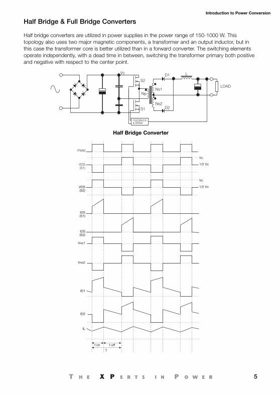
Half Bridge & Full Bridge Converters
Half bridge converters are utilized in power supplies in the power range of 150-1000 W. Thistopology also uses two major magnetic components, a transformer and an output inductor, but inthis case the transformer core is better utilized than in a forward converter. The switching elementsoperate independently, with a dead time in between, switching the transformer primary both positiveand negative with respect to the center point.
FEEDBACK& DRIVE
LOAD
Vc
NpNs1
Ns2D2
D1 L
S1
S2
Half Bridge Converter
PWM
VDS(S1)
Vc
1/2 Vc
IDS(S1)
VDS(S2)
Vc
1/2 Vc
IDS(S2)
VNS2
VNS1
ID1
ID2
t on t off
T
IL
Intro_280110.qxp:Layout 1 21/6/10 09:33 Page 5
6
Introduction to Power Conversion
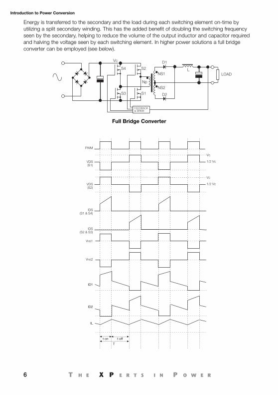
Energy is transferred to the secondary and the load during each switching element on-time byutilizing a split secondary winding. This has the added benefit of doubling the switching frequencyseen by the secondary, helping to reduce the volume of the output inductor and capacitor requiredand halving the voltage seen by each switching element. In higher power solutions a full bridgeconverter can be employed (see below).
FEEDBACK& DRIVE
LOAD
Vc
S4 S2
S3 S1 D2
NS2
NS1
Np
D1
L
Full Bridge Converter
PWM
VDS(S1)
Vc
1/2 Vc
IDS(S1 & S4)
IDS(S2 & S3)
VDS(S2)
Vc
1/2 Vc
VNS2
VNS1
ID1
ID2
t on t off
T
IL
Intro_280110.qxp:Layout 1 21/6/10 09:33 Page 6
7
Introduction to Power Conversion
LOADNp1
Np2
Ns1
Ns2
D2S1S2
D1 L
FEEDBACK& DRIVE
This topology will provide double the output power for the same primary switching current, butincreases the complexity of switching element drive circuits, compared to the half bridge. Half bridgeand full bridge converters are used in AC input power supplies. There is also a trend to utilize thistopology in low voltage bus converters.
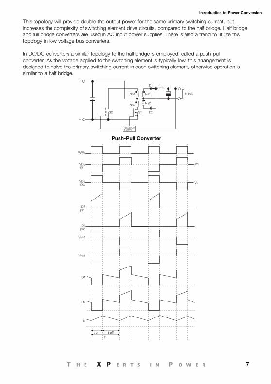
In DC/DC converters a similar topology to the half bridge is employed, called a push-pullconverter. As the voltage applied to the switching element is typically low, this arrangement isdesigned to halve the primary switching current in each switching element, otherwise operation issimilar to a half bridge.
Push-Pull Converter
PWM
VDS(S1)
VDS(S2)
Vc
Vc
IDS(S1)
ID1(S2)
VNS2
VNS1
ID1
ID2
t on t off
T
IL
Intro_280110.qxp:Layout 1 21/6/10 09:34 Page 7
8
Introduction to Power Conversion
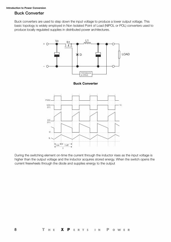
Buck Converter
Buck converters are used to step down the input voltage to produce a lower output voltage. Thisbasic topology is widely employed in Non Isolated Point of Load (NIPOL or POL) converters used toproduce locally regulated supplies in distributed power architectures.
LOAD
Vc S1 L1
D
FEEDBACK& DRIVE
Buck Converter
During the switching element on-time the current through the inductor rises as the input voltage ishigher than the output voltage and the inductor acquires stored energy. When the switch opens thecurrent freewheels through the diode and supplies energy to the output
PWM
IDS(S1)
VDS(S1)
Vc
ID
t on t off
T
IL
Intro_280110.qxp:Layout 1 21/6/10 09:34 Page 8
9
Introduction to Power Conversion
LOAD
FEEDBACK& DRIVE
D
S1
L1Vc
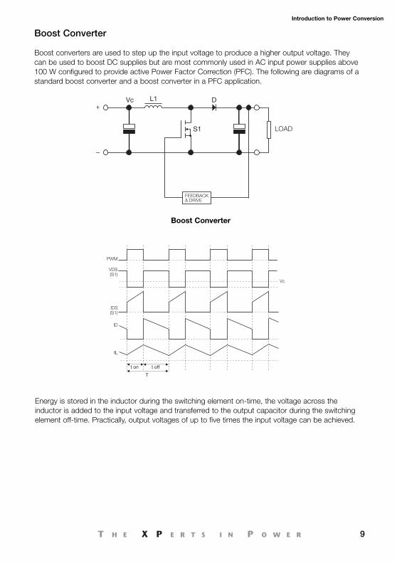
Boost Converter
Boost converters are used to step up the input voltage to produce a higher output voltage. Theycan be used to boost DC supplies but are most commonly used in AC input power supplies above100 W configured to provide active Power Factor Correction (PFC). The following are diagrams of astandard boost converter and a boost converter in a PFC application.
Boost Converter
PWM
IDS(S1)
VDS(S1)
Vc
ID
t on t off
T
IL
Energy is stored in the inductor during the switching element on-time, the voltage across theinductor is added to the input voltage and transferred to the output capacitor during the switchingelement off-time. Practically, output voltages of up to five times the input voltage can be achieved.
Intro_280110.qxp:Layout 1 21/6/10 09:34 Page 9
10
Introduction to Power Conversion
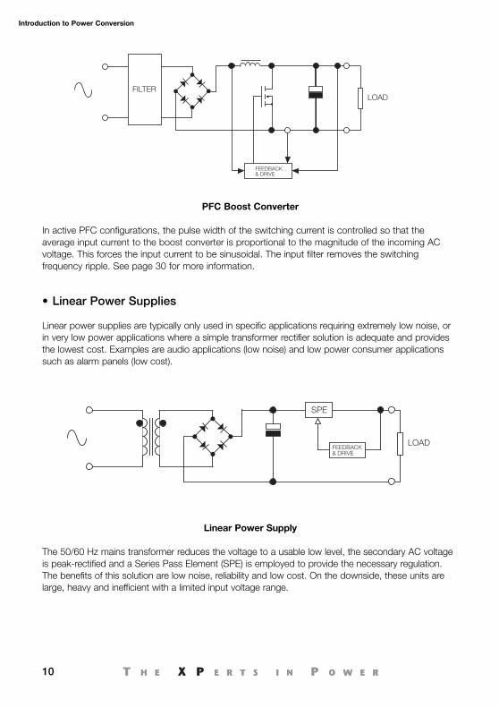
PFC Boost Converter
In active PFC configurations, the pulse width of the switching current is controlled so that theaverage input current to the boost converter is proportional to the magnitude of the incoming ACvoltage. This forces the input current to be sinusoidal. The input filter removes the switchingfrequency ripple. See page 30 for more information.
• Linear Power Supplies
Linear power supplies are typically only used in specific applications requiring extremely low noise, orin very low power applications where a simple transformer rectifier solution is adequate and providesthe lowest cost. Examples are audio applications (low noise) and low power consumer applicationssuch as alarm panels (low cost).
Linear Power Supply
The 50/60 Hz mains transformer reduces the voltage to a usable low level, the secondary AC voltageis peak-rectified and a Series Pass Element (SPE) is employed to provide the necessary regulation.The benefits of this solution are low noise, reliability and low cost. On the downside, these units arelarge, heavy and inefficient with a limited input voltage range.
LOADFILTER
FEEDBACK& DRIVE
FEEDBACK& DRIVE
LOAD
SPE
Intro_280110.qxp:Layout 1 21/6/10 09:34 Page 10
11
Introduction to Power Conversion
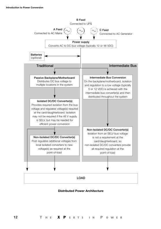
• Distributed Power Architecture
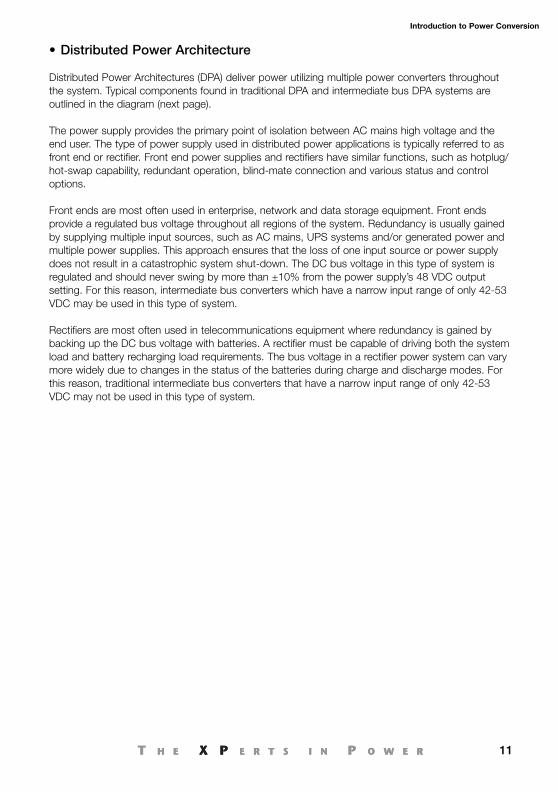
Distributed Power Architectures (DPA) deliver power utilizing multiple power converters throughoutthe system. Typical components found in traditional DPA and intermediate bus DPA systems areoutlined in the diagram (next page).
The power supply provides the primary point of isolation between AC mains high voltage and theend user. The type of power supply used in distributed power applications is typically referred to asfront end or rectifier. Front end power supplies and rectifiers have similar functions, such as hotplug/hot-swap capability, redundant operation, blind-mate connection and various status and controloptions.
Front ends are most often used in enterprise, network and data storage equipment. Front endsprovide a regulated bus voltage throughout all regions of the system. Redundancy is usually gainedby supplying multiple input sources, such as AC mains, UPS systems and/or generated power andmultiple power supplies. This approach ensures that the loss of one input source or power supplydoes not result in a catastrophic system shut-down. The DC bus voltage in this type of system isregulated and should never swing by more than ±10% from the power supply’s 48 VDC outputsetting. For this reason, intermediate bus converters which have a narrow input range of only 42-53VDC may be used in this type of system.
Rectifiers are most often used in telecommunications equipment where redundancy is gained bybacking up the DC bus voltage with batteries. A rectifier must be capable of driving both the systemload and battery recharging load requirements. The bus voltage in a rectifier power system can varymore widely due to changes in the status of the batteries during charge and discharge modes. Forthis reason, traditional intermediate bus converters that have a narrow input range of only 42-53VDC may not be used in this type of system.
Intro_280110.qxp:Layout 1 21/6/10 09:34 Page 11
12
Introduction to Power Conversion
Distributed Power Architecture
Intermediate Bus
A FeedConnected to AC Mains
B FeedConnected to UPS
C FeedConnected to AC Generator
Power supplyConverts AC to DC bus voltage (typically 12 or 48 VDC)
Batteries(optional)
LOAD
Passive Backplane/MotherboardDistributes DC bus voltage to
multiple locations in the system
Isolated DC/DC Converter(s)Provides required isolation from the busvoltage and regulates voltage(s) required
at the card/daughterboard. Isolation may not be required if the 48 V supply
is SELV, but may be needed for efficient power conversion
Non-Isolated DC/DC Converter(s)Post regulates additional voltages from
local isolated converters to newvoltage(s) as required at the
point-of-load
Traditional
Intermediate Bus ConversionOn the backplane/motherboard, isolationand regulation to a low voltage (typically
5 or 12 VDC) is achieved with theintermediate bus converter(s) and then
distributed throughout the system
Non-Isolated DC/DC Converter(s)Isolation from an SELV bus voltage
is not a requirement at thecard/daughterboard, so
non-isolated DC/DC converters provideall required regulation at the
point-of-load
Intro_280110.qxp:Layout 1 21/6/10 09:34 Page 12
13
Input Considerations
• Power Sources
Sources of electricity (most notably rotary electro-mechanical generators) naturally produce voltagesalternating in polarity, reversing positive and negative over time, known as alternating current (AC).AC power is typically derived from the local power company grids, either as single or three-phasesource. This is then converted to DC within the majority of electronic equipment.
AC Power Sources
In applications where electricity is used to dissipate energy in the form of heat (heaters, light bulbs),the polarity or direction of current is irrelevant so long as there is enough voltage and current to theload to produce the desired heat (power dissipation). However, with AC it is possible to build electricgenerators, motors and power distribution systems that are far more efficient than a DC equivalent.For this reason, AC is used predominantly in high power applications.
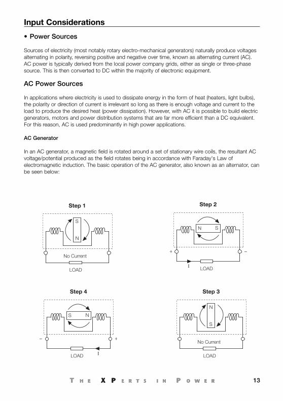
AC Generator
In an AC generator, a magnetic field is rotated around a set of stationary wire coils, the resultant ACvoltage/potential produced as the field rotates being in accordance with Faraday's Law ofelectromagnetic induction. The basic operation of the AC generator, also known as an alternator, canbe seen below:
LOAD
No Current
Step 1
N
S
LOADI
Step 2
N S
LOAD
No Current
Step 3
S
N
LOAD
Step 4
S N
I
InputConsid_080210.qxp:Layout 1 21/6/10 10:20 Page 13
14
Input Considerations
The polarity of the voltage across the wire coils reverses as the opposite poles of the rotating magnetpass by. Connected to a load, this reversing voltage polarity creates a reversing current direction inthe circuit.
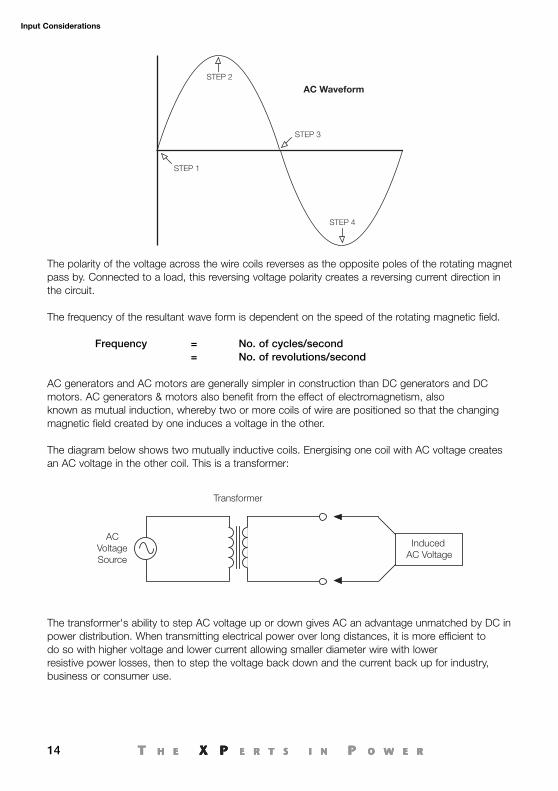
The frequency of the resultant wave form is dependent on the speed of the rotating magnetic field.
Frequency = No. of cycles/second= No. of revolutions/second
AC generators and AC motors are generally simpler in construction than DC generators and DCmotors. AC generators & motors also benefit from the effect of electromagnetism, alsoknown as mutual induction, whereby two or more coils of wire are positioned so that the changingmagnetic field created by one induces a voltage in the other.
The diagram below shows two mutually inductive coils. Energising one coil with AC voltage createsan AC voltage in the other coil. This is a transformer:
The transformer's ability to step AC voltage up or down gives AC an advantage unmatched by DC inpower distribution. When transmitting electrical power over long distances, it is more efficient todo so with higher voltage and lower current allowing smaller diameter wire with lowerresistive power losses, then to step the voltage back down and the current back up for industry,business or consumer use.
STEP 1
STEP 2
STEP 3
STEP 4
AC Waveform
ACVoltageSource
Transformer
Induced AC Voltage
InputConsid_080210.qxp:Layout 1 21/6/10 10:20 Page 14
15
Input Considerations
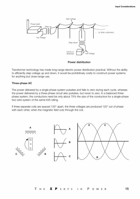
Transformer technology has made long-range electric power distribution practical. Without the abilityto efficiently step voltage up and down, it would be prohibitively costly to construct power systemsfor anything but close-range use.
Three-phase AC
The power delivered by a single-phase system pulsates and falls to zero during each cycle, whereasthe power delivered by a three-phase circuit also pulsates, but never to zero. In a balanced three-phase system, the conductors need be only about 75% the size of the conductors for a single-phasetwo-wire system of the same kVA rating.
If three separate coils are spaced 120° apart, the three voltages are produced 120° out of phasewith each other, when the magnetic field cuts through the coil.
Power plant
low voltage
low voltage
Step-up
Step-down
Home orBusiness
high voltage
. . . to other customers
A
BC
S
N
A
B
C
A
B
C
Power distribution
InputConsid_080210.qxp:Layout 1 21/6/10 10:20 Page 15
16
Input Considerations
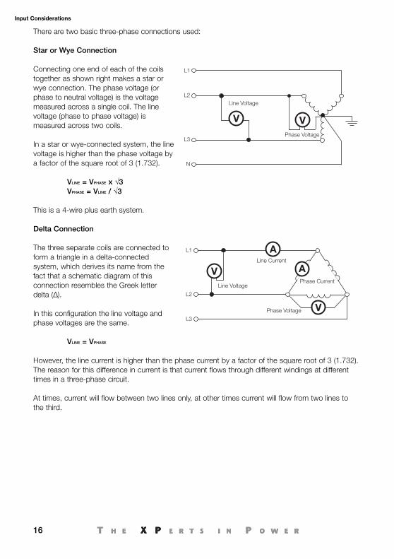
There are two basic three-phase connections used:
Star or Wye Connection
Connecting one end of each of the coilstogether as shown right makes a star orwye connection. The phase voltage (orphase to neutral voltage) is the voltagemeasured across a single coil. The linevoltage (phase to phase voltage) ismeasured across two coils.
In a star or wye-connected system, the linevoltage is higher than the phase voltage by a factor of the square root of 3 (1.732).
VLINE = VPHASE x √3VPHASE = VLINE / √3
This is a 4-wire plus earth system.
Delta Connection
The three separate coils are connected toform a triangle in a delta-connectedsystem, which derives its name from thefact that a schematic diagram of thisconnection resembles the Greek letterdelta (Δ).
In this configuration the line voltage andphase voltages are the same.
VLINE = VPHASE
However, the line current is higher than the phase current by a factor of the square root of 3 (1.732).The reason for this difference in current is that current flows through different windings at differenttimes in a three-phase circuit.
At times, current will flow between two lines only, at other times current will flow from two lines to the third.
Line Voltage
L1
L2
L3
N
Phase Voltage
VV
Line Voltage
Line Current
Phase Current
L1
L2
L3Phase Voltage
A
AV
V
InputConsid_080210.qxp:Layout 1 21/6/10 10:20 Page 16
17
Input Considerations
220-240 V / 50 Hz
220-240 V / 60 Hz
100-127 V / 60 Hz
100-127 V / 50 Hz
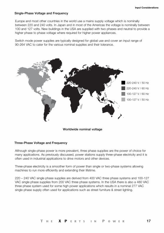
Single-Phase Voltage and Frequency
Europe and most other countries in the world use a mains supply voltage which is nominallybetween 220 and 240 volts. In Japan and in most of the Americas the voltage is nominally between100 and 127 volts. New buildings in the USA are supplied with two phases and neutral to provide ahigher phase to phase voltage where required for higher power appliances.
Switch mode power supplies are typically designed for global use and cover an input range of 90-264 VAC to cater for the various nominal supplies and their tolerance.
Three-Phase Voltage and Frequency
Although single-phase power is more prevalent, three phase supplies are the power of choice formany applications. As previously discussed, power stations supply three-phase electricity and it isoften used in industrial applications to drive motors and other devices.
Three-phase electricity is a smoother form of power than single or two-phase systems allowingmachines to run more efficiently and extending their lifetime.
220 – 240 VAC single phase supplies are derived from 400 VAC three phase systems and 100-127VAC single phase supplies from 200 VAC three phase systems. In the USA there is also a 480 VACthree phase system used for some high power applications which results in a nominal 277 VACsingle phase supply often used for applications such as street furniture & street lighting.
Worldwide nominal voltage
InputConsid_080210.qxp:Layout 1 21/6/10 10:20 Page 17
18
Input Considerations
DC Power Sources
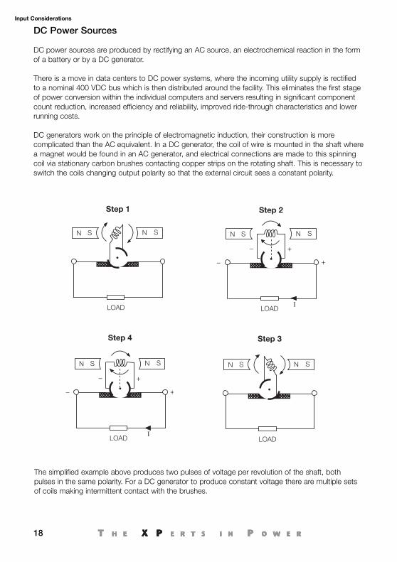
DC power sources are produced by rectifying an AC source, an electrochemical reaction in the formof a battery or by a DC generator.
There is a move in data centers to DC power systems, where the incoming utility supply is rectifiedto a nominal 400 VDC bus which is then distributed around the facility. This eliminates the first stageof power conversion within the individual computers and servers resulting in significant componentcount reduction, increased efficiency and reliability, improved ride-through characteristics and lowerrunning costs.
DC generators work on the principle of electromagnetic induction, their construction is morecomplicated than the AC equivalent. In a DC generator, the coil of wire is mounted in the shaft wherea magnet would be found in an AC generator, and electrical connections are made to this spinningcoil via stationary carbon brushes contacting copper strips on the rotating shaft. This is necessary toswitch the coils changing output polarity so that the external circuit sees a constant polarity.
LOAD
Step 1
N SSN
Step 2
LOADI
N SSN
Step 3
LOAD
N SSN
Step 4
LOAD
N SSN
I
The simplified example above produces two pulses of voltage per revolution of the shaft, bothpulses in the same polarity. For a DC generator to produce constant voltage there are multiple setsof coils making intermittent contact with the brushes.
InputConsid_080210.qxp:Layout 1 21/6/10 10:20 Page 18
19
Input Considerations
Batteries
There are four battery chemistries in common use; Valve Regulated Lead Acid (VRLA), NickelCadmium (NiCad), Nickel Metal Hydride (NiMH) & Lithium (Lithium Ion & Lithium Polymer).
Valve Regulated Lead Acid
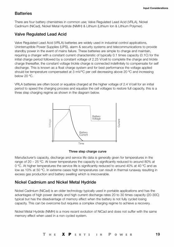
Valve Regulated Lead Acid (VRLA) batteries are widely used in industrial control applications,Uninterruptible Power Supplies (UPS), alarm & security systems and telecommunications to providestandby power in the event of mains failure. These batteries are simple to charge and maintain,requiring a charger with a constant current characteristic of typically 0.1 times capacity (0.1C) for theinitial charge period followed by a constant voltage of 2.25 V/cell to complete the charge and tricklecharge thereafter, the constant voltage trickle charge is connected indefinitely to compensate for selfdischarge. This is known as a float charge system and for best performance the voltage appliedshould be temperature compensated at 3 mV/ºC per cell decreasing above 20 ºC and increasingbelow 20 ºC.
VRLA batteries are often boost or equalize charged at the higher voltage of 2.4 V/cell for an initialperiod to speed the charging process and equalize the cell voltages to restore full capacity, this is athree step charging regime as shown in the diagram below.
Manufacturer’s capacity, discharge and service life data is generally given for temperatures in therange of 20 – 25 ºC. At lower temperatures the capacity is significantly reduced to around 80% at 0 ºC. At higher temperatures the service life is significantly reduced to around 40% at 40 ºC and aslow as 10% at 50 ºC. In extreme cases high temperatures can result in thermal runaway resulting inexcess gas production and battery swelling which is irrecoverable.
Nickel Cadmium and Nickel Metal Hydride
Nickel Cadmium (NiCad) is an older technology typically used in portable applications and has theadvantages of high power density and high current discharge rates 20 to 30 times capacity (20-30C)typical but has the disadvantage of memory effect when the battery is not fully cycled losingcapacity. This can be overcome but requires a complex charging regime to achieve a recovery.
Nickel Metal Hydride (NiMH) is a more recent evolution of NiCad and does not suffer with the samememory effect when used in a non cycled system.
Curr
ent
Voltage
BatteryVoltage
BatteryCurrent
Time
Three step charge curve
InputConsid_080210.qxp:Layout 1 21/6/10 10:20 Page 19
20
Input Considerations
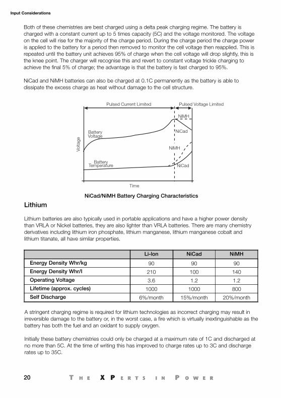
Both of these chemistries are best charged using a delta peak charging regime. The battery ischarged with a constant current up to 5 times capacity (5C) and the voltage monitored. The voltageon the cell will rise for the majority of the charge period. During the charge period the charge poweris applied to the battery for a period then removed to monitor the cell voltage then reapplied. This isrepeated until the battery unit achieves 95% of charge when the cell voltage will drop slightly, this isthe knee point. The charger will recognise this and revert to constant voltage trickle charging toachieve the final 5% of charge; the advantage is that the battery is fast charged to 95%.
NiCad and NiMH batteries can also be charged at 0.1C permanently as the battery is able todissipate the excess charge as heat without damage to the cell structure.
Lithium
Lithium batteries are also typically used in portable applications and have a higher power densitythan VRLA or Nickel batteries, they are also lighter than VRLA batteries. There are many chemistryderivatives including lithium iron phosphate, lithium manganese, lithium manganese cobalt andlithium titanate, all have similar properties.
Voltage
Time
BatteryVoltage
Pulsed Current Limited Pulsed Voltage Limited
NiMH
NiCad
NiCadBattery
Temperature
NiMH
NiCad/NiMH Battery Charging Characteristics
Li-lon NiCad NiMH
Energy Density Whr/kg 90 90 90Energy Density Whr/I 210 100 140Operating Voltage 3.6 1.2 1.2Lifetime (approx. cycles) 1000 1000 800Self Discharge 6%/month 15%/month 20%/month
A stringent charging regime is required for lithium technologies as incorrect charging may result inirreversible damage to the battery or, in the worst case, a fire which is virtually inextinguishable as thebattery has both the fuel and an oxidant to supply oxygen.
Initially these battery chemistries could only be charged at a maximum rate of 1C and discharged atno more than 5C. At the time of writing this has improved to charge rates up to 3C and dischargerates up to 35C.
InputConsid_080210.qxp:Layout 1 21/6/10 10:20 Page 20
21
Input Considerations
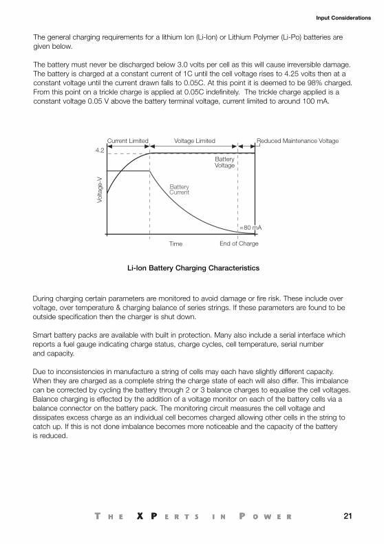
The general charging requirements for a lithium Ion (Li-Ion) or Lithium Polymer (Li-Po) batteries aregiven below.
The battery must never be discharged below 3.0 volts per cell as this will cause irreversible damage.The battery is charged at a constant current of 1C until the cell voltage rises to 4.25 volts then at aconstant voltage until the current drawn falls to 0.05C. At this point it is deemed to be 98% charged.From this point on a trickle charge is applied at 0.05C indefinitely. The trickle charge applied is aconstant voltage 0.05 V above the battery terminal voltage, current limited to around 100 mA.
Voltage-V
Time End of Charge
BatteryVoltage
4.2
BatteryCurrent
80 mA~~
Reduced Maintenance VoltageVoltage LimitedCurrent Limited
Li-lon Battery Charging Characteristics
During charging certain parameters are monitored to avoid damage or fire risk. These include overvoltage, over temperature & charging balance of series strings. If these parameters are found to beoutside specification then the charger is shut down.
Smart battery packs are available with built in protection. Many also include a serial interface whichreports a fuel gauge indicating charge status, charge cycles, cell temperature, serial number and capacity.
Due to inconsistencies in manufacture a string of cells may each have slightly different capacity.When they are charged as a complete string the charge state of each will also differ. This imbalancecan be corrected by cycling the battery through 2 or 3 balance charges to equalise the cell voltages.Balance charging is effected by the addition of a voltage monitor on each of the battery cells via abalance connector on the battery pack. The monitoring circuit measures the cell voltage anddissipates excess charge as an individual cell becomes charged allowing other cells in the string tocatch up. If this is not done imbalance becomes more noticeable and the capacity of the battery is reduced.
InputConsid_080210.qxp:Layout 1 21/6/10 10:20 Page 21
22
Input Considerations
• Input Protection
Input Current Protection
Input protection is implemented in power supplies and DC/DC converters to ensure safe operation.The input fuse fitted within a power supply is not intended to be field-replaceable, it is rated suchthat only a catastrophic failure of the power supply will cause it to fail. It will not be cleared by anoverload as the power supply will have some other form of overload protection, usually electronic.The fuse will often be soldered into the PCB rather than being a replaceable cartridge type fuse.
The power supply fuse is listed as a critical part of the safety approval process and is used to ensurethat the power supply does not catch fire under a fault condition. If the fuse clears the most likelycause is that the converter has failed short circuit presenting a short circuit to the mains supply. Inthis event the fuse will clear very quickly.
As previously discussed, the fuse in the power supply is not intended to be field-replaceable, andshould only be replaced by competent service personnel following repair. When using a componentpower supply, there will be additional mains wiring within the enclosure before the power supply andits fuse. This is where an additional fuse or circuit breaker as a protection device is fitted to ensurethat the wiring and associated componentsdo not present a hazard.
When the end equipment is testedfor safety it will also go through faultanalysis to ensure that it will not present afire hazard under a fault condition. If a faultwere to occur many hundreds of Amps canflow causing wires to heat up very quickly,causing noxious fumes from the meltingplastic insulation and creating a potential fire hazard.
Input Voltage Protection
The input of the equipment may be subjected to a number of transient voltage conditions. Thesediffer between AC & DC systems.
AC Systems Switching transientsLightning strikesSpikes
DC Systems Engine cranking transientsDC line transientsReverse polarity
The AC system transients are catered for in the EN61000-4-x series of standards. The DC transientsrelate to DC systems in vehicle, traction and telecommunications applications. See page 27.
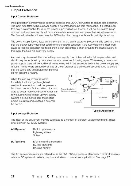
Power Supply
Application
Enclosure
Power distributionFire hazard
Typical Application
InputConsid_080210.qxp:Layout 1 21/6/10 10:20 Page 22
23
Input Considerations
Typical DC/DC converter input circuit
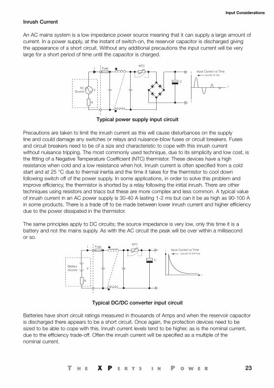
Inrush Current
An AC mains system is a low impedance power source meaning that it can supply a large amount ofcurrent. In a power supply, at the instant of switch-on, the reservoir capacitor is discharged givingthe appearance of a short circuit. Without any additional precautions the input current will be verylarge for a short period of time until the capacitor is charged.
Precautions are taken to limit the inrush current as this will cause disturbances on the supplyline and could damage any switches or relays and nuisance-blow fuses or circuit breakers. Fusesand circuit breakers need to be of a size and characteristic to cope with this inrush currentwithout nuisance tripping. The most commonly used technique, due to its simplicity and low cost, isthe fitting of a Negative Temperature Coefficient (NTC) thermistor. These devices have a highresistance when cold and a low resistance when hot. Inrush current is often specified from a coldstart and at 25 °C due to thermal inertia and the time it takes for the thermistor to cool downfollowing switch off of the power supply. In some applications, in order to solve this problem andimprove efficiency, the thermistor is shorted by a relay following the initial inrush. There are othertechniques using resistors and triacs but these are more complex and less common. A typical valueof inrush current in an AC power supply is 30-40 A lasting 1-2 ms but can it be as high as 90-100 Ain some products. There is a trade off to be made between lower inrush current and higher efficiencydue to the power dissipated in the thermistor.
The same principles apply to DC circuits; the source impedance is very low, only this time it is abattery and not the mains supply. As with the AC circuit the peak will be over within a millisecond or so.
Batteries have short circuit ratings measured in thousands of Amps and when the reservoir capacitoris discharged there appears to be a short circuit. Once again, the protection devices need to besized to be able to cope with this. Inrush current levels tend to be higher, as is the nominal current,due to the efficiency trade-off. Often the inrush current will be specified as a multiple of the nominal current.
Typical power supply input circuit
Fuse
R
V
I
Battery Source
NTC
C
I
T
typically 30-40A Peak
Input Current vs Time
Fuse
R
V
I
AC Source
NTC
C
typically 30-40A
Input Current vs Time
I
I
t
InputConsid_080210.qxp:Layout 1 21/6/10 10:20 Page 23
24
Input Considerations
Sizing of Fuses & Circuit Breakers
So that the rating of the fuse or breaker can be determined, the nominal input current of the powersupply needs to be established. If the application has more than one power supply or other mainspowered equipment these will need to be taken into account.
To determine the input current, we need first to determine the input power and, in AC systems,remember to take into account the power factor.
Input Power = Output Power / Efficiency
Input Current = (Input Power / Input Voltage) / Power Factor
Choose fuse or CB rating at least 1.5 x Input Current - Time Lag
It is advisable to use a time lag fuse or breaker to avoid nuisance tripping on start up. The 1.5 x inputcurrent rating is to overcome the ageing effects of fuses.
Fuses are rated FF, F, T, TT (ranging from super fast to long time lag). For power supplies it isrecommended that T or TT types are used.
Circuit breakers are A-K (very fast to long time delay). For power supplies, C or above would be recommended.
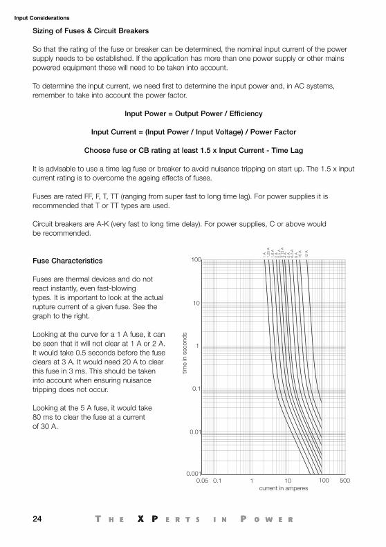
Fuse Characteristics
Fuses are thermal devices and do notreact instantly, even fast-blowingtypes. It is important to look at the actualrupture current of a given fuse. See thegraph to the right.
Looking at the curve for a 1 A fuse, it canbe seen that it will not clear at 1 A or 2 A.It would take 0.5 seconds before the fuseclears at 3 A. It would need 20 A to clearthis fuse in 3 ms. This should be takeninto account when ensuring nuisancetripping does not occur.
Looking at the 5 A fuse, it would take80 ms to clear the fuse at a current of 30 A.
5001001010.10.050.001
0.01
0.1
1
10
100
current in amperes
time
in s
econ
ds
1 A
1.25
A1.
6 A
2 A
2.5
A3.
15 A
4 A
5 A
6.3
A8
A10
A
12 A
InputConsid_080210.qxp:Layout 1 21/6/10 10:20 Page 24
25
Input Considerations
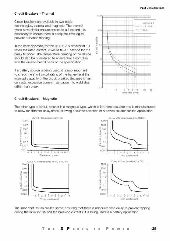
Circuit Breakers - Thermal
Circuit breakers are available in two basictechnologies, thermal and magnetic. The thermaltypes have similar characteristics to a fuse and it isnecessary to ensure there is adequate time lag toprevent nuisance tripping.
In the case opposite, for the 0.05-2.7 A breaker at 10times the rated current, it would take 1 second for thebreak to occur. The temperature derating of the deviceshould also be considered to ensure that it complieswith the environmental parts of the specification.
If a battery source is being used, it is also importantto check the short circuit rating of the battery and theinterrupt capacity of the circuit breaker. Because it hascontacts, excessive current may cause it to weld shutrather than break.
Circuit Breakers – Magnetic
The other type of circuit breaker is a magnetic type, which is far more accurate and is manufacturedto allow for different delay times, allowing accurate selection of a device suitable for the application.
The important issues are the same; ensuring that there is adequate time delay to prevent trippingduring the initial inrush and the breaking current if it is being used in a battery application.
4084210.1
1
10
100
1000
10000
Times rated current
Trip
tim
e in
sec
onds
6 10 20
0.05 - 2.7 A
2.8 - 25 A
25 A
0 1 2 3 4 5 6 7 8 9 10 11 120.001
0.01
0.1
1
10
100
1000
1000
Times rated current
Trip
tim
e in
sec
onds
Curve F1 (Instantaneous) for DC
0 1 2 3 4 5 6 7 8 9 10 11 120.001
0.01
0.1
1
10
100
1000
1000
Times rated current
Trip
tim
e in
sec
onds
Curve M0 (medium delay) for AC/DC
0 1 2 3 4 5 6 7 8 9 10 11 120.001
0.01
0.1
1
10
100
1000
1000
Times rated current
Trip
tim
e in
sec
onds
Curve F2 (Instantaneous) for AC 50/60 Hz
0 1 2 3 4 5 6 7 8 9 10 11 120.001
0.01
0.1
1
10
100
1000
1000
Times rated current
Trip
tim
e in
sec
onds
Curve M1 (medium delay) for DC
InputConsid_080210.qxp:Layout 1 21/6/10 10:20 Page 25
26
Input Considerations
Input Voltage Transient Protection
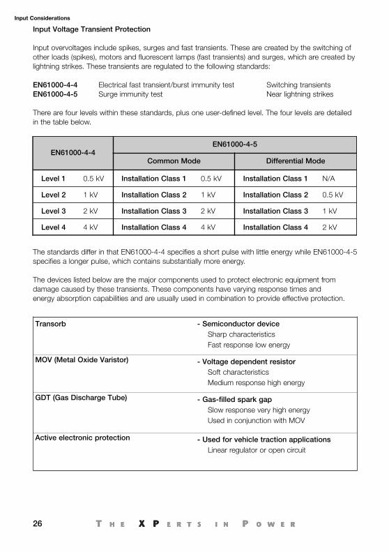
Input overvoltages include spikes, surges and fast transients. These are created by the switching ofother loads (spikes), motors and fluorescent lamps (fast transients) and surges, which are created bylightning strikes. These transients are regulated to the following standards:
EN61000-4-4 Electrical fast transient/burst immunity test Switching transientsEN61000-4-5 Surge immunity test Near lightning strikes
There are four levels within these standards, plus one user-defined level. The four levels are detailedin the table below.
The standards differ in that EN61000-4-4 specifies a short pulse with little energy while EN61000-4-5specifies a longer pulse, which contains substantially more energy.
The devices listed below are the major components used to protect electronic equipment fromdamage caused by these transients. These components have varying response times andenergy absorption capabilities and are usually used in combination to provide effective protection.
Transorb - Semiconductor deviceSharp characteristicsFast response low energy
MOV (Metal Oxide Varistor) - Voltage dependent resistorSoft characteristicsMedium response high energy
GDT (Gas Discharge Tube) - Gas-filled spark gapSlow response very high energyUsed in conjunction with MOV
Active electronic protection - Used for vehicle traction applicationsLinear regulator or open circuit
EN61000-4-4EN61000-4-5
Common Mode Differential Mode
Level 1 0.5 kV Installation Class 1 0.5 kV Installation Class 1 N/A
Level 2 1 kV Installation Class 2 1 kV Installation Class 2 0.5 kV
Level 3 2 kV Installation Class 3 2 kV Installation Class 3 1 kV
Level 4 4 kV Installation Class 4 4 kV Installation Class 4 2 kV
InputConsid_080210.qxp:Layout 1 21/6/10 10:20 Page 26
27
Input Considerations
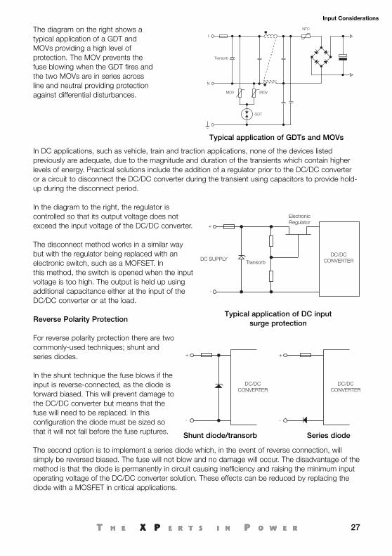
The diagram on the right shows atypical application of a GDT andMOVs providing a high level ofprotection. The MOV prevents thefuse blowing when the GDT fires andthe two MOVs are in series acrossline and neutral providing protectionagainst differential disturbances.
In DC applications, such as vehicle, train and traction applications, none of the devices listedpreviously are adequate, due to the magnitude and duration of the transients which contain higherlevels of energy. Practical solutions include the addition of a regulator prior to the DC/DC converteror a circuit to disconnect the DC/DC converter during the transient using capacitors to provide hold-up during the disconnect period.
In the diagram to the right, the regulator iscontrolled so that its output voltage does notexceed the input voltage of the DC/DC converter.
The disconnect method works in a similar waybut with the regulator being replaced with anelectronic switch, such as a MOFSET. Inthis method, the switch is opened when the inputvoltage is too high. The output is held up usingadditional capacitance either at the input of theDC/DC converter or at the load.
Reverse Polarity Protection
For reverse polarity protection there are twocommonly-used techniques; shunt andseries diodes.
In the shunt technique the fuse blows if theinput is reverse-connected, as the diode isforward biased. This will prevent damage tothe DC/DC converter but means that thefuse will need to be replaced. In thisconfiguration the diode must be sized sothat it will not fail before the fuse ruptures.
The second option is to implement a series diode which, in the event of reverse connection, willsimply be reversed biased. The fuse will not blow and no damage will occur. The disadvantage of themethod is that the diode is permanently in circuit causing inefficiency and raising the minimum inputoperating voltage of the DC/DC converter solution. These effects can be reduced by replacing thediode with a MOSFET in critical applications.
L
N
Transorb
NTC
MOV
GDT
MOV
DC SUPPLYTransorb
DC/DC CONVERTER
Electronic Regulator
+
-
DC/DC CONVERTER
DC/DC CONVERTER
+
-
+
-
Typical application of GDTs and MOVs
Typical application of DC input surge protection
Shunt diode/transorb Series diode
InputConsid_080210.qxp:Layout 1 21/6/10 10:20 Page 27
28
Input Considerations
• AC Input Current & Harmonics
Power Supply Harmonic Distortion
As a result of the peak rectification techniques used in power supplies, harmonic currents aregenerated. To limit these harmonics, legislation has been introduced. The relevant standard isEN61000-3-2 for equipment with an input current ≤16 A per phase.
EN61000-3-2 establishes four classes of equipment, each with their own limits for harmonic emissions.
Class D - T.V.’s, personal computers & monitors consuming ≤600 WClass C - Lighting equipmentClass B - Portable toolsClass A - Everything else
Equipment Classes A & B have absolute limits for harmonics whatever the input power, Class Cequipment has limits expressed as a percentage of the 50 Hz current consumed and for Class Dequipment the harmonic current limits are proportional to the mains power consumed. Equipmentcategorized in Classes C & D will normally require a power supply incorporating active power factor correction.
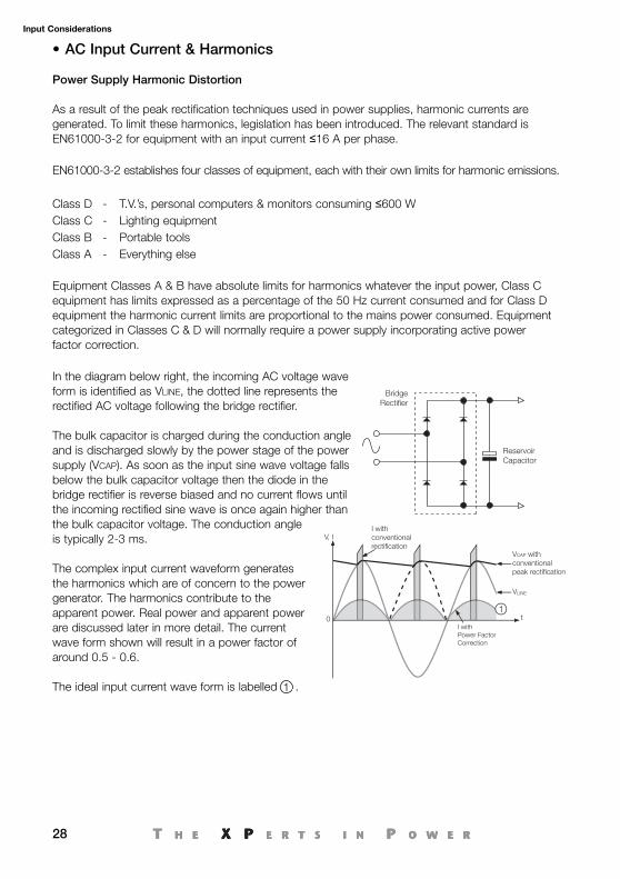
In the diagram below right, the incoming AC voltage waveform is identified as VLINE, the dotted line represents therectified AC voltage following the bridge rectifier.
The bulk capacitor is charged during the conduction angleand is discharged slowly by the power stage of the powersupply (VCAP). As soon as the input sine wave voltage fallsbelow the bulk capacitor voltage then the diode in thebridge rectifier is reverse biased and no current flows untilthe incoming rectified sine wave is once again higher thanthe bulk capacitor voltage. The conduction angleis typically 2-3 ms.
The complex input current waveform generatesthe harmonics which are of concern to the powergenerator. The harmonics contribute to theapparent power. Real power and apparent powerare discussed later in more detail. The currentwave form shown will result in a power factor ofaround 0.5 - 0.6.
The ideal input current wave form is labelled .
VLINE
VCAP withconventionalpeak rectification
t0
I withconventionalrectification
V, I
1
I with Power FactorCorrection
ReservoirCapacitor
BridgeRectifier
1
InputConsid_080210.qxp:Layout 1 21/6/10 10:20 Page 28
29
Input Considerations
Why is Harmonic Distortion a Problem?
The utility provider must supply the voltage and all of the current, even though some of the current isnot turned into useful output power – See the section entitled Real and Apparent Power on page 31.The provider has no means of charging for the extra current because the power is charged in kWh.
The combined effect of millions of power supplies is to clip the AC voltage because all of the currentis drawn at the peak of the sine wave. Power conductors must be sized to carry the extra currentcaused by the low power factor. Neutral conductors can overheat because they are typically notsized to carry all of the harmonic currents which do not exist for high power factor loads.
Solutions for Power Supplies
In order to meet the legislation for harmonic distortion there are two main solutions available forpower supplies:
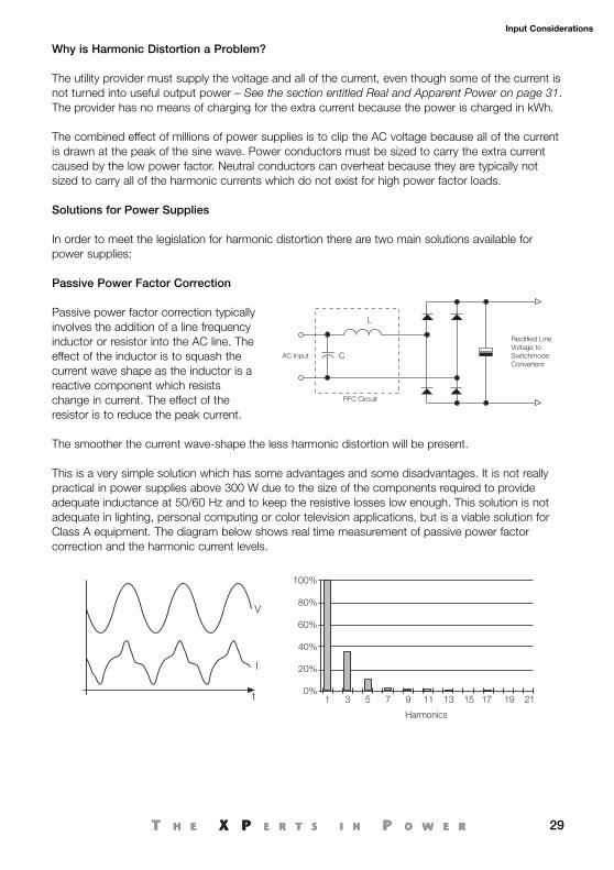
Passive Power Factor Correction
Passive power factor correction typicallyinvolves the addition of a line frequencyinductor or resistor into the AC line. Theeffect of the inductor is to squash thecurrent wave shape as the inductor is areactive component which resistschange in current. The effect of theresistor is to reduce the peak current.
The smoother the current wave-shape the less harmonic distortion will be present.
This is a very simple solution which has some advantages and some disadvantages. It is not reallypractical in power supplies above 300 W due to the size of the components required to provideadequate inductance at 50/60 Hz and to keep the resistive losses low enough. This solution is notadequate in lighting, personal computing or color television applications, but is a viable solution forClass A equipment. The diagram below shows real time measurement of passive power factorcorrection and the harmonic current levels.
AC Input
PFC Circuit
Rectified LineVoltage toSwitchmodeConverters
L
C
1 3 5 7 9 11 13 15 17 19 21
100%
80%
60%
40%
20%
0%t
I
V
Harmonics
InputConsid_080210.qxp:Layout 1 21/6/10 10:20 Page 29
30
Input Considerations
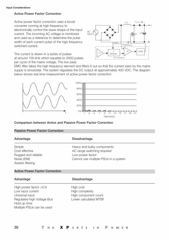
Active Power Factor Correction
Active power factor correction uses a boostconverter running at high frequency toelectronically control the wave-shape of the inputcurrent. The incoming AC voltage is monitoredand used as a reference to determine the pulsewidth of each current pulse of the high frequencyswitched current.
The current is drawn in a series of pulsesat around 100 kHz which equates to 2000 pulsesper cycle of the mains voltage. The low passEMC filter takes the high frequency element and filters it out so that the current seen by the mainssupply is sinusoidal. The system regulates the DC output at approximately 400 VDC. The diagrambelow shows real time measurement of active power factor correction.
Comparison between Active and Passive Power Factor Correction
Passive Power Factor Correction
Advantage Disadvantage
Simple Heavy and bulky componentsCost effective AC range switching requiredRugged and reliable Low power factorNoise (EMI) Cannot use multiple PSUs in a systemAssists filtering
Active Power Factor Correction
Advantage Disadvantage
High power factor >0.9 High costLow input current High complexityUniversal input High component countRegulated high Voltage Bus Lower calculated MTBFHold up timeMultiple PSUs can be used
ACInput
L1
Q1 C1
VIN Sense
Current Sense
VFeedback
+
-
PWMU1
+
- U2+
-
MultiplierX
PFC Controller IC
100%
80%
60%
40%
20%
0%t
V
I
Harmonics1 3 5 7 9 11 13 15 17 19 21
31
Input Considerations
• Real and Apparent Power
What is Power?
Power is simply the rate at which work is done. The more power available in a system, the morework can be completed in the same period of time. In terms of electricity, increasing power meansthe ability to do more electrical work (energy) in the same number of seconds, for example, runningmore appliances, spinning a motor faster, or running a faster CPU. Power is measured in Watts (W).One Watt equals one Joule of energy expended in one second:
Power (W) = Work or Energy (J) / Time (seconds)
Conversely, the amount of energy used by a device can be computed as the amount of power ituses multiplied by the length of time over which that power is applied:
Work or Energy (J) = Power (W) x Time (seconds)
Computing electrical power can be very simple or very complicated. With direct current, power (inWatts) is just the product of the voltage (in Volts) and the current (in Amps) of the circuit:
P (W) = V (V) x I (A)
More work is done when electrons push with more force (higher voltage) and when there are moreof them per period of time (higher current). Since P = V x I, and I = V/R, another way to expresspower is:
P = V2 / R
In a DC system power is measured and calculated as shown above. In an AC system it is morecomplicated because phase shift and wave form shape must be taken into consideration.
Real Power
Real, true or active power is the measurement of power dissipated in the load.
It can be shown as:
P (W) = V (V) x I (A)
Real power is measured in Watts.
InputConsid_080210.qxp:Layout 1 21/6/10 10:20 Page 31
32
Input Considerations
Reactive Power
Reactive power is power which is merely supplied to the load and returned to the source, rather thanbeing dissipated in the load.
This is caused by the reactive elements in an AC circuit, specifically inductors and capacitors whichtend to charge and discharge during normal operation.
Reactive power is measured as Volt-Amps-reactive (VAr).
Apparent Power
This is the total power in a circuit at any one time. It includes both dissipated (real) and returned(reactive) power.
Apparent power is measured in Volt-Amps (VA).
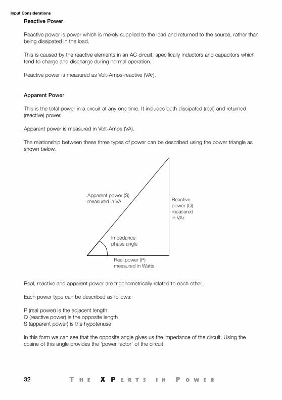
The relationship between these three types of power can be described using the power triangle asshown below.
Real, reactive and apparent power are trigonometrically related to each other.
Each power type can be described as follows:
P (real power) is the adjacent lengthQ (reactive power) is the opposite lengthS (apparent power) is the hypotenuse
In this form we can see that the opposite angle gives us the impedance of the circuit. Using thecosine of this angle provides the ‘power factor’ of the circuit.
Apparent power (S)measured in VA
Real power (P)measured in Watts
Impedancephase angle
Reactive power (Q)measured in VAr
InputConsid_080210.qxp:Layout 1 21/6/10 10:20 Page 32
33
Input Considerations
What is Power Factor?
Power factor is a characteristic of AC circuits only. It is always a number between zero and one, thecloser to one, the better the system’s power factor.
Power Factor = Real Power/Apparent Power
Using the previously discussed data, it is now possible to add in this third element to the formula:
Power (W) = Apparent Power (VA) x Power Factor (PF)
Apparent Power (VA) = Power (W)/Power Factor (PF)
Power factor is a measure of the efficiency of energy transfer from source to load. The greater theefficiency the closer to unity power factor.
If power is not being dissipated in the load but simply circulates round the reactive elements of thecircuit (inductors and capacitors), then energy transfer is not as efficient and the power factor will beless than unity.
Two key elements affect the power factor of any system. These are known as phase shift and harmonics.
Effects of Phase Shift on Power Factor
To understand how phase shift affects the power factor of any system, here are a couple of practical examples:
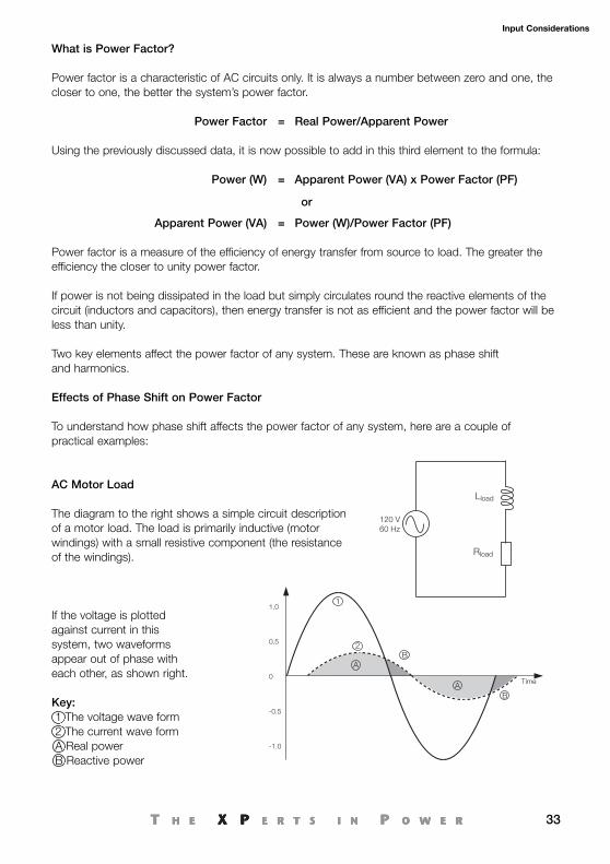
AC Motor Load
The diagram to the right shows a simple circuit descriptionof a motor load. The load is primarily inductive (motorwindings) with a small resistive component (the resistanceof the windings).
If the voltage is plottedagainst current in thissystem, two waveformsappear out of phase witheach other, as shown right.
Key:1 The voltage wave form2 The current wave formA Real powerB Reactive power
1.0
0.5
0
-0.5
-1.0
Time
A
1
2B
BA
Lload
Rload
120 V60 Hz
or
InputConsid_080210.qxp:Layout 1 21/6/10 10:20 Page 33
34
Input Considerations
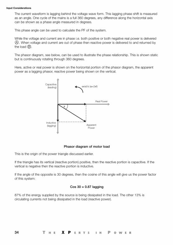
The current waveform is lagging behind the voltage wave form. This lagging phase shift is measuredas an angle. One cycle of the mains is a full 360 degrees, any difference along the horizontal axiscan be shown as a phase angle measured in degrees.
This phase angle can be used to calculate the PF of the system.
While the voltage and current are in phase i.e. both positive or both negative real power is delivered. When voltage and current are out of phase then reactive power is delivered to and returned by
the load .
The phasor diagram, see below, can be used to illustrate the phase relationship. This is shown staticbut is continuously rotating through 360 degrees.
Here, active or real power is shown on the horizontal portion of the phasor diagram, the apparentpower as a lagging phasor, reactive power being shown on the vertical.
This is the origin of the power triangle discussed earlier.
If the triangle has its vertical (reactive portion) positive, then the reactive portion is capacitive. If thevertical is negative then the reactive portion is inductive.
If the angle of the opposite is 30 degrees, then the cosine of this angle will give us the power factorof this system:
Cos 30 = 0.87 lagging
87% of the energy supplied by the source is being dissipated in the load. The other 13% iscirculating currents not being dissipated in the load (reactive power).
Capacitive(leading)
Inductive(lagging)
Real Power
ApparentPower
ωrad/s (ω=2πf)
θ
AB
Phasor diagram of motor load
InputConsid_080210.qxp:Layout 1 21/6/10 10:21 Page 34
35
Input Considerations
AC Resistive Load
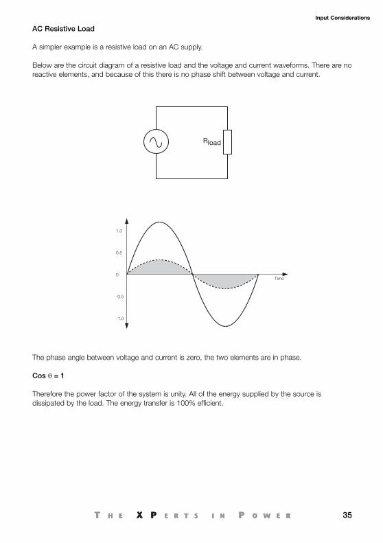
A simpler example is a resistive load on an AC supply.
Below are the circuit diagram of a resistive load and the voltage and current waveforms. There are noreactive elements, and because of this there is no phase shift between voltage and current.
The phase angle between voltage and current is zero, the two elements are in phase.
Cos θ = 1
Therefore the power factor of the system is unity. All of the energy supplied by the source isdissipated by the load. The energy transfer is 100% efficient.
Rload
1.0
0.5
0
-0.5
-1.0
Time
InputConsid_080210.qxp:Layout 1 21/6/10 10:21 Page 35
36
Input Considerations
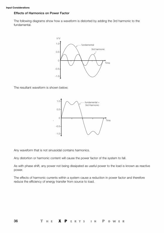
Effects of Harmonics on Power Factor
The following diagrams show how a waveform is distorted by adding the 3rd harmonic to thefundamental.
The resultant waveform is shown below;
Any waveform that is not sinusoidal contains harmonics.
Any distortion or harmonic content will cause the power factor of the system to fall.
As with phase shift, any power not being dissipated as useful power to the load is known as reactivepower.
The effects of harmonic currents within a system cause a reduction in power factor and thereforereduce the efficiency of energy transfer from source to load.
e0
0.5
Time
fundamental +3rd Harmonic
-0.5
1.0
-1.0
0
0.5
Time
V/ V
fundamental
-0.5
1.0
-1.0
3rd harmonic
InputConsid_080210.qxp:Layout 1 21/6/10 10:21 Page 36
37
Input Considerations
Effects of a Low System Power Factor
Both phase shift and harmonics can cause a reduction in the power factor of the system.
This reduction in power factor means that more current has to be generated at source to deliver thepower to the load. This in turn means that, unless power factor correction is applied to loads, anumber of problems are caused.
Power factor correction can be either passive or active. Whichever form it takes, it will be used toensure that the amount of harmonics specifically within a system is reduced; this will increase thepower factor of the system and increase the source-load energy transfer efficiency.
In phase shift applications (e.g. motor load), passive power factor correction can be applied (addinginductance or capacitance to circuit) to correct any phase shift between voltage and current. Thisagain will increase source-load energy transfer efficiency.
Common examples of problems with low power factors within a system can be seen in the list below:
Mains voltage distortion Caused by harmonics which can cause problems such aslight flicker.
Oversizing of conductors Necessary as circulating currents must also be allowed forwhen cable sizing.
Overheating of neutral conductors Caused because protection is generally in the livewire only.
Electromagnetic load failures Generally occur when harmonics present cause themagnetic device to heat up.
Circuit breakers tripping Circulating currents, due to reactive power, not considered.
InputConsid_080210.qxp:Layout 1 21/6/10 10:21 Page 37
38
Input Considerations
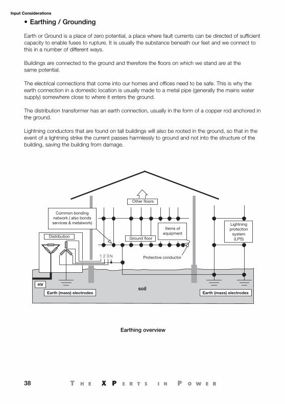
• Earthing / Grounding
Earth or Ground is a place of zero potential, a place where fault currents can be directed of sufficientcapacity to enable fuses to rupture. It is usually the substance beneath our feet and we connect tothis in a number of different ways.
Buildings are connected to the ground and therefore the floors on which we stand are at the same potential.
The electrical connections that come into our homes and offices need to be safe. This is why theearth connection in a domestic location is usually made to a metal pipe (generally the mains watersupply) somewhere close to where it enters the ground.
The distribution transformer has an earth connection, usually in the form of a copper rod anchored inthe ground.
Lightning conductors that are found on tall buildings will also be rooted in the ground, so that in theevent of a lightning strike the current passes harmlessly to ground and not into the structure of thebuilding, saving the building from damage.
1 2 3 N
soil Earth (mass) electrodes Earth (mass) electrodes
HV
Protective conductor
Other floors
Ground floor Distribution
Items of equipment
Common bonding network ( also bonds services & metalwork) Lightning
protection system (LPS)
Earthing overview
InputConsid_080210.qxp:Layout 1 21/6/10 10:21 Page 38
39
Input Considerations
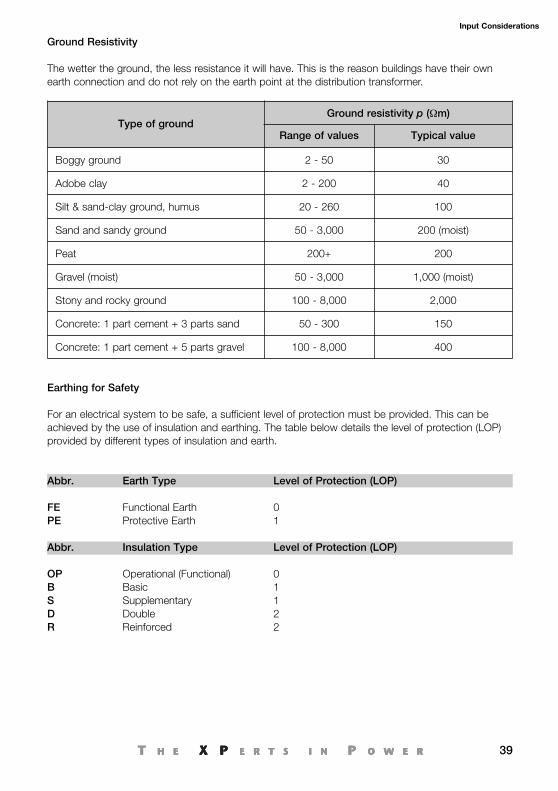
Ground Resistivity
The wetter the ground, the less resistance it will have. This is the reason buildings have their ownearth connection and do not rely on the earth point at the distribution transformer.
Earthing for Safety
For an electrical system to be safe, a sufficient level of protection must be provided. This can beachieved by the use of insulation and earthing. The table below details the level of protection (LOP)provided by different types of insulation and earth.
Abbr. Earth Type Level of Protection (LOP)
FE Functional Earth 0PE Protective Earth 1
Abbr. Insulation Type Level of Protection (LOP)
OP Operational (Functional) 0B Basic 1S Supplementary 1D Double 2R Reinforced 2
Type of groundGround resistivity p (Ωm)
Range of values Typical value
Boggy ground 2 - 50 30
Adobe clay 2 - 200 40
Silt & sand-clay ground, humus 20 - 260 100
Sand and sandy ground 50 - 3,000 200 (moist)
Peat 200+ 200
Gravel (moist) 50 - 3,000 1,000 (moist)
Stony and rocky ground 100 - 8,000 2,000
Concrete: 1 part cement + 3 parts sand 50 - 300 150
Concrete: 1 part cement + 5 parts gravel 100 - 8,000 400
InputConsid_080210.qxp:Layout 1 21/6/10 10:21 Page 39
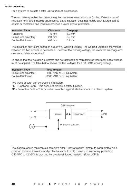
For a system to be safe a total LOP of 2 must be provided.
The next table specifies the distance required between two conductors for the different types ofinsulation for IT and industrial applications. Basic insulation does not require such a large gap asdouble or reinforced and therefore provides a lower level of protection.
Insulation Type Clearance CreepageFunctional 1.5 mm 3.2 mmBasic/Supplementary 2.0 mm 3.2 mmDouble/Reinforced 4.0 mm 6.4 mm
The distances above are based on a 300 VAC working voltage. The working voltage is the voltagebetween the two circuits to be isolated. The lower the working voltage, the lower the creepage andclearance distances required.
To ensure that the insulation is correct and not damaged or manufactured incorrectly a test voltagemust be applied. The table below shows the test voltages for a 300 VAC working voltage.
Insulation Type Test VoltageBasic/Supplementary 1500 VAC or DC equivalentDouble/Reinforced 3000 VAC or DC equivalent
Two types of earth can be present in a system.FE – Functional Earth – This does not provide a safety function. PE – Protective Earth – This provides protection against electric shock in a class 1 system.
The diagram above represents a complete class 1 power supply. Primary to earth protection isprovided by basic insulation and protective earth (LOP 2). Primary to secondary protection(240 VAC to 12 VDC) is provided by double/reinforced insulation (Total LOP 2).
LOAD L
N
PE
Primary
D/R Insulation
B (Basic insulation)
Secondary
Input Considerations
40
InputConsid_080210.qxp:Layout 1 21/6/10 10:21 Page 40
41
DC Output Considerations
• Output Regulation
Line Regulation
Line regulation is a static performance measure of changes in output voltage due to changes of theinput voltage. It defines the change in output voltage or current resulting from a change in the inputvoltage over a specified range and is normally expressed as a percentage.
% Line Regulation =
where VOUT(Nominal) is the output voltage at nominal line input voltageVOUT(Max) is the maximum output voltage measured over the specified input rangeVOUT(Min) is the minimum output voltage measured over the specified input range
Load Regulation and Cross Regulation
Load regulation is the static performance measure, which defines the ability of a power supply toremain within specified output limits for a predetermined load change. Expressed as a percentage,the range is dependent upon the product design and is specified in the product data sheet.
% Load Regulation =
where VOUT(Nominal) is the nominal output voltageVOUT(Load Max) is the output voltage at maximum output currentVOUT(Load Min) is the output voltage at minimum output current
For multiple output power supplies, another factor affecting the output voltage is cross regulation.This is an extension of the load regulation test and determines the ability of all of the power supplyoutputs to remain within their specified voltage rating for a load current change on another output. Itis calculated in the same manner as load regulation and is often specified as a percentage change inoutput voltage for a percentage change in another output load, e.g. V1cross regulation = 1% per10% change in V2.
Example: A power supply’s output voltage is nominally 5.02 V butwhen the AC input is varied from its minimum to maximum valuethe output varies from 5.015 V to 5.03 V.
% Line Regulation =
Example: A power supply manufacturer specifies that for a loadchange of 5% to 100% its power supply output changes from5.05 V to 5.02 V around a nominal voltage of 5.02 V.
% Load Regulation =
VOUT(Max)-VOUT(Min)
VOUT(Nominal)x 100( (
5.03 - 5.0155.02
x 100 = 0.29%( (
VOUT(Load Max)-VOUT(Load Min)
VOUT(Nominal)x 100( (
5.05 - 5.025.02
x 100 = 0.6%( (
42
DC Output Considerations
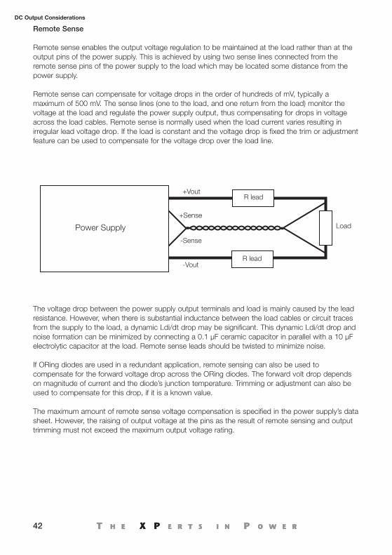
Remote Sense
Remote sense enables the output voltage regulation to be maintained at the load rather than at theoutput pins of the power supply. This is achieved by using two sense lines connected from theremote sense pins of the power supply to the load which may be located some distance from thepower supply.
Remote sense can compensate for voltage drops in the order of hundreds of mV, typically amaximum of 500 mV. The sense lines (one to the load, and one return from the load) monitor thevoltage at the load and regulate the power supply output, thus compensating for drops in voltageacross the load cables. Remote sense is normally used when the load current varies resulting inirregular lead voltage drop. If the load is constant and the voltage drop is fixed the trim or adjustmentfeature can be used to compensate for the voltage drop over the load line.
The voltage drop between the power supply output terminals and load is mainly caused by the leadresistance. However, when there is substantial inductance between the load cables or circuit tracesfrom the supply to the load, a dynamic Ldi/dt drop may be significant. This dynamic Ldi/dt drop andnoise formation can be minimized by connecting a 0.1 µF ceramic capacitor in parallel with a 10 µFelectrolytic capacitor at the load. Remote sense leads should be twisted to minimize noise.
If ORing diodes are used in a redundant application, remote sensing can also be used tocompensate for the forward voltage drop across the ORing diodes. The forward volt drop dependson magnitude of current and the diode’s junction temperature. Trimming or adjustment can also beused to compensate for this drop, if it is a known value.
The maximum amount of remote sense voltage compensation is specified in the power supply’s datasheet. However, the raising of output voltage at the pins as the result of remote sensing and outputtrimming must not exceed the maximum output voltage rating.
Load
R lead
R lead+Vout
-Vout
+Sense
-Sense
Power Supply
43
DC Output Considerations
Transient Load Response
Transient response measures how quickly and effectively the power supply can adjust to suddenchanges in current demand. The figure below shows the behavior of a typical converter during aload-current transient and the resultant output voltage wave form.
The output filter of a switching regulator, excluding flyback converters, is composed of an inductorand capacitor which is a second-order lag system. Therefore, it takes a finite time to recover fromload current transients and settle to its new output voltage.
The transient load response is normally specified as a maximum percentage change and recoverytime of the output to a step load change, e.g. 4% maximum deviation, 500 µs recovery for a 25%step load change.
• High Peak Loads
Some power supplies specify a peak load capability to support loads that are higher than thenominal continuous power for short periods. In these applications the average power required istypically significantly lower than the peak demand.
Applications that require high peak currents include print heads, pumps, motors, and disk drives.These products are found in factory automation, medical pumping systems, fluid and materialhandling, robotics, power tools, machining, packaging, test, dispensing systems & printers.
Using a power supply that is capable of supporting high peak loads will result in a physically smallerpower supply reducing system size, weight and cost. In a system that requires 800 W for a shortduration, using a 400 W power supply with an 800 W peak rating will result in significant savings involume and cost over a supply rated at 800 W continuous power.
t0
100%
75%
Loadcurrent
t
+200 mV
5 VDC
-200 mV
Outputvoltage
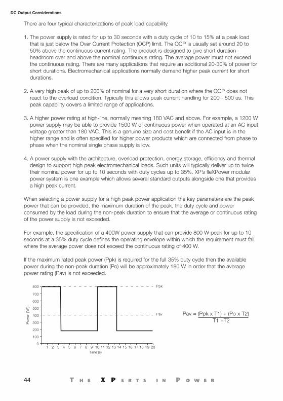
44
DC Output Considerations
There are four typical characterizations of peak load capability.
1. The power supply is rated for up to 30 seconds with a duty cycle of 10 to 15% at a peak loadthat is just below the Over Current Protection (OCP) limit. The OCP is usually set around 20 to50% above the continuous current rating. The product is designed to give short durationheadroom over and above the nominal continuous rating. The average power must not exceedthe continuous rating. There are many applications that require an additional 20-30% of power forshort durations. Electromechanical applications normally demand higher peak current for shortdurations.
2. A very high peak of up to 200% of nominal for a very short duration where the OCP does notreact to the overload condition. Typically this allows peak current handling for 200 - 500 us. Thispeak capability covers a limited range of applications.
3. A higher power rating at high-line, normally meaning 180 VAC and above. For example, a 1200 Wpower supply may be able to provide 1500 W of continuous power when operated at an AC inputvoltage greater than 180 VAC. This is a genuine size and cost benefit if the AC input is in thehigher range and is often specified for higher power products which are connected from phase tophase when the nominal single phase supply is low.
4. A power supply with the architecture, overload protection, energy storage, efficiency and thermaldesign to support high peak electromechanical loads. Such units will typically deliver up to twicetheir nominal power for up to 10 seconds with duty cycles up to 35%. XP’s fleXPower modularpower system is one example which allows several standard outputs alongside one that providesa high peak current.
When selecting a power supply for a high peak power application the key parameters are the peakpower that can be provided, the maximum duration of the peak, the duty cycle and powerconsumed by the load during the non-peak duration to ensure that the average or continuous ratingof the power supply is not exceeded.
For example, the specification of a 400W power supply that can provide 800 W peak for up to 10seconds at a 35% duty cycle defines the operating envelope within which the requirement must fallwhere the average power does not exceed the continuous rating of 400 W.
If the maximum rated peak power (Ppk) is required for the full 35% duty cycle then the availablepower during the non-peak duration (Po) will be approximately 180 W in order that the averagepower rating (Pav) is not exceeded.
1 2 3 4 5 6 7 8 9 10 11 12 13 14 15 16 17 18 19 200
100
200
300
400
500
600
700
800
Time (s)
Ppk
Pav
Pow
er(W
)
Pav = (Ppk x T1) + (Po x T2)T1 +T2
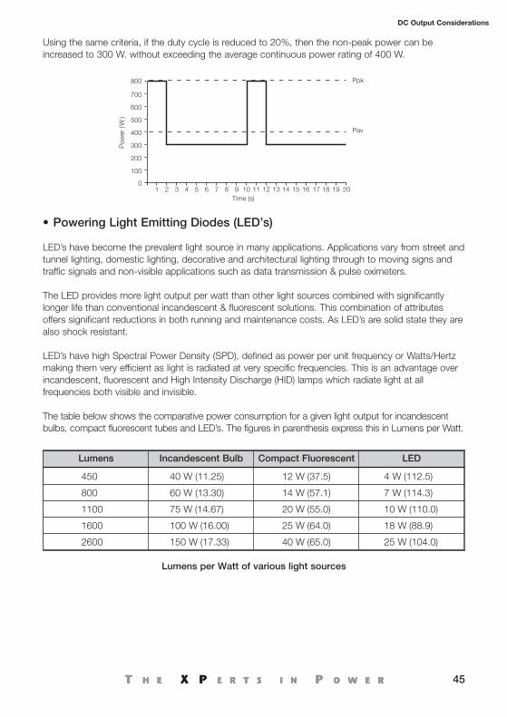
45
DC Output Considerations
Using the same criteria, if the duty cycle is reduced to 20%, then the non-peak power can beincreased to 300 W. without exceeding the average continuous power rating of 400 W.
1 2 3 4 5 6 7 8 9 10 11 12 13 14 15 16 17 18 19 200
100
200
300
400
500
600
700
800
Time (s)
Ppk
PavP
ower
(W)
• Powering Light Emitting Diodes (LED’s)
LED’s have become the prevalent light source in many applications. Applications vary from street andtunnel lighting, domestic lighting, decorative and architectural lighting through to moving signs andtraffic signals and non-visible applications such as data transmission & pulse oximeters.
The LED provides more light output per watt than other light sources combined with significantlylonger life than conventional incandescent & fluorescent solutions. This combination of attributesoffers significant reductions in both running and maintenance costs. As LED’s are solid state they arealso shock resistant.
LED’s have high Spectral Power Density (SPD), defined as power per unit frequency or Watts/Hertzmaking them very efficient as light is radiated at very specific frequencies. This is an advantage overincandescent, fluorescent and High Intensity Discharge (HID) lamps which radiate light at allfrequencies both visible and invisible.
The table below shows the comparative power consumption for a given light output for incandescentbulbs, compact fluorescent tubes and LED’s. The figures in parenthesis express this in Lumens per Watt.
Lumens Incandescent Bulb Compact Fluorescent LED
450 40 W (11.25) 12 W (37.5) 4 W (112.5)
800 60 W (13.30) 14 W (57.1) 7 W (114.3)
1100 75 W (14.67) 20 W (55.0) 10 W (110.0)
1600 100 W (16.00) 25 W (64.0) 18 W (88.9)
2600 150 W (17.33) 40 W (65.0) 25 W (104.0)
Lumens per Watt of various light sources
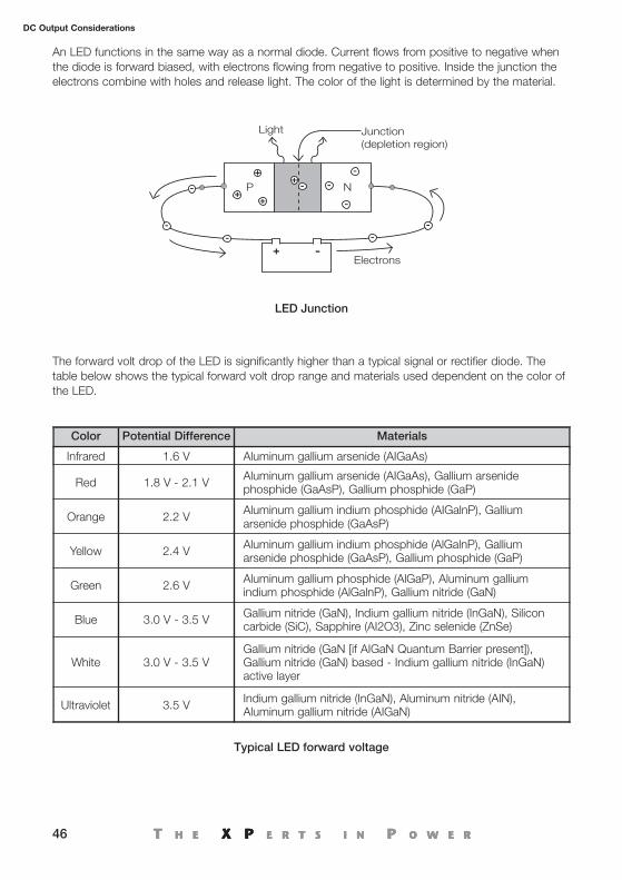
46
DC Output Considerations
An LED functions in the same way as a normal diode. Current flows from positive to negative whenthe diode is forward biased, with electrons flowing from negative to positive. Inside the junction theelectrons combine with holes and release light. The color of the light is determined by the material.
Electrons+ -
Light Junction(depletion region)
P N
--
-
--
-
--
-+
++
+
LED Junction
Typical LED forward voltage
Color Potential Difference Materials
Infrared 1.6 V Aluminum gallium arsenide (AIGaAs)
Red 1.8 V - 2.1 V Aluminum gallium arsenide (AIGaAs), Gallium arsenidephosphide (GaAsP), Gallium phosphide (GaP)
Orange 2.2 V Aluminum gallium indium phosphide (AIGalnP), Galliumarsenide phosphide (GaAsP)
Yellow 2.4 V Aluminum gallium indium phosphide (AlGalnP), Galliumarsenide phosphide (GaAsP), Gallium phosphide (GaP)
Green 2.6 V Aluminum gallium phosphide (AlGaP), Aluminum galliumindium phosphide (AlGalnP), Gallium nitride (GaN)
Blue 3.0 V - 3.5 V Gallium nitride (GaN), Indium gallium nitride (InGaN), Siliconcarbide (SiC), Sapphire (AI2O3), Zinc selenide (ZnSe)
White 3.0 V - 3.5 VGallium nitride (GaN [if AIGaN Quantum Barrier present]),Gallium nitride (GaN) based - Indium gallium nitride (InGaN)active layer
Ultraviolet 3.5 V Indium gallium nitride (InGaN), Aluminum nitride (AIN),Aluminum gallium nitride (AIGaN)
The forward volt drop of the LED is significantly higher than a typical signal or rectifier diode. Thetable below shows the typical forward volt drop range and materials used dependent on the color ofthe LED.
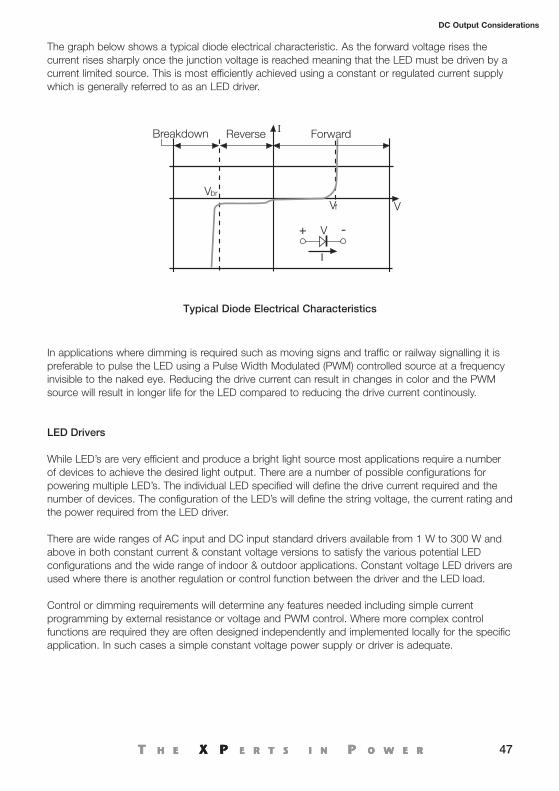
47
DC Output Considerations
The graph below shows a typical diode electrical characteristic. As the forward voltage rises thecurrent rises sharply once the junction voltage is reached meaning that the LED must be driven by acurrent limited source. This is most efficiently achieved using a constant or regulated current supplywhich is generally referred to as an LED driver.
ReverseBreakdown ForwardI
I
Vbr
V
V -+
Vf
Typical Diode Electrical Characteristics
In applications where dimming is required such as moving signs and traffic or railway signalling it ispreferable to pulse the LED using a Pulse Width Modulated (PWM) controlled source at a frequencyinvisible to the naked eye. Reducing the drive current can result in changes in color and the PWMsource will result in longer life for the LED compared to reducing the drive current continously.
LED Drivers
While LED’s are very efficient and produce a bright light source most applications require a numberof devices to achieve the desired light output. There are a number of possible configurations forpowering multiple LED’s. The individual LED specified will define the drive current required and thenumber of devices. The configuration of the LED’s will define the string voltage, the current rating andthe power required from the LED driver.
There are wide ranges of AC input and DC input standard drivers available from 1 W to 300 W andabove in both constant current & constant voltage versions to satisfy the various potential LEDconfigurations and the wide range of indoor & outdoor applications. Constant voltage LED drivers areused where there is another regulation or control function between the driver and the LED load.
Control or dimming requirements will determine any features needed including simple currentprogramming by external resistance or voltage and PWM control. Where more complex controlfunctions are required they are often designed independently and implemented locally for the specificapplication. In such cases a simple constant voltage power supply or driver is adequate.
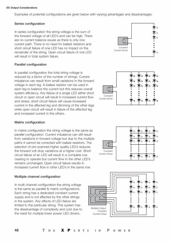
48
DC Output Considerations
ConstantCurrent Driver
Multiple OutputConstant
Current Driver
ConstantCurrent Driver
Examples of potential configurations are given below with varying advantages and disadvantages.
Series configuration
In series configuration the string voltage is the sum ofthe forward voltage of all LED’s and can be high. Thereare no current balance issues as there is only onecurrent path. There is no need for ballast resistors andshort circuit failure of one LED has no impact on theremainder of the string. Open circuit failure of one LEDwill result in total system failure.
Parallel configuration
In parallel configuration the total string voltage isreduced by a factor of the number of strings. Currentimbalance can result from small variations in the forwardvoltage in each leg. A ballast resistor can be used ineach leg to balance the current but this reduces overallsystem efficiency. Any failure of a single LED either shortcircuit or open circuit will result in increased current flowand stress; short circuit failure will cause increasedcurrent in the affected leg and dimming of the other legswhile open circuit will result in failure of the affected legand increased current in the others.
Matrix configuration
In matrix configuration the string voltage is the same asparallel configuration. Current imbalance can still resultfrom variations in forward voltage but due to the multiplepaths it cannot be corrected with ballast resistors. Theselection of pre-scanned higher quality LED’s reducesthe forward volt drop variations at a higher cost. Shortcircuit failure of an LED will result in a complete rowceasing to operate but current flow in the other LED’sremains unchanged. Open circuit failure results inincreased current flow in other LED’s in the same row.
Multiple channel configuration
In multi channel configuration the string voltageis the same as parallel & matrix configurations.Each string has a dedicated constant currentsupply and is not affected by the other stringsin the system. Any effects of LED failure arelimited to the particular string. This system hasthe disadvantage of complexity and cost due tothe need for multiple lower power LED drivers.
ConstantCurrent Driver
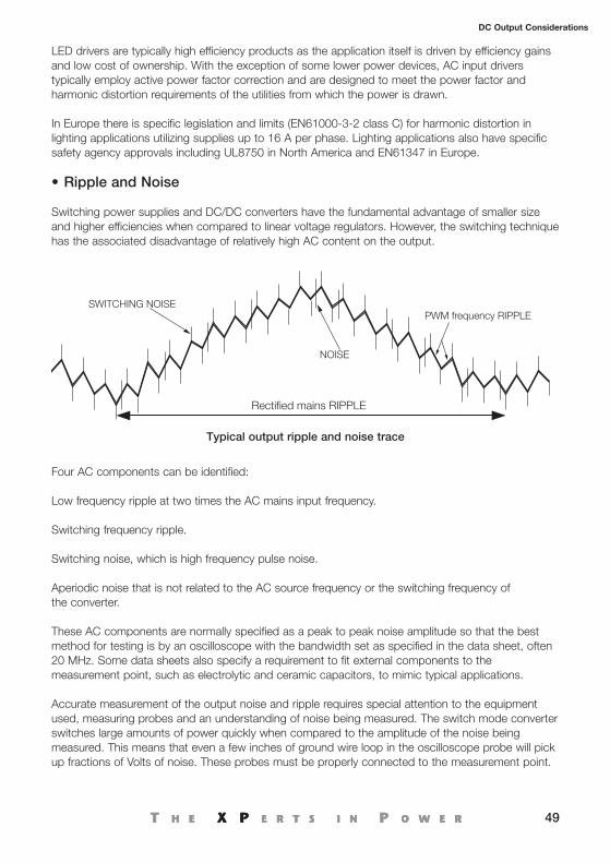
49
DC Output Considerations
• Ripple and Noise
Switching power supplies and DC/DC converters have the fundamental advantage of smaller sizeand higher efficiencies when compared to linear voltage regulators. However, the switching techniquehas the associated disadvantage of relatively high AC content on the output.
Rectified mains RIPPLE
NOISE
SWITCHING NOISEPWM frequency RIPPLE
Typical output ripple and noise trace
LED drivers are typically high efficiency products as the application itself is driven by efficiency gainsand low cost of ownership. With the exception of some lower power devices, AC input driverstypically employ active power factor correction and are designed to meet the power factor andharmonic distortion requirements of the utilities from which the power is drawn.
In Europe there is specific legislation and limits (EN61000-3-2 class C) for harmonic distortion inlighting applications utilizing supplies up to 16 A per phase. Lighting applications also have specificsafety agency approvals including UL8750 in North America and EN61347 in Europe.
Four AC components can be identified:
Low frequency ripple at two times the AC mains input frequency.
Switching frequency ripple.
Switching noise, which is high frequency pulse noise.
Aperiodic noise that is not related to the AC source frequency or the switching frequency ofthe converter.
These AC components are normally specified as a peak to peak noise amplitude so that the bestmethod for testing is by an oscilloscope with the bandwidth set as specified in the data sheet, often20 MHz. Some data sheets also specify a requirement to fit external components to themeasurement point, such as electrolytic and ceramic capacitors, to mimic typical applications.
Accurate measurement of the output noise and ripple requires special attention to the equipmentused, measuring probes and an understanding of noise being measured. The switch mode converterswitches large amounts of power quickly when compared to the amplitude of the noise beingmeasured. This means that even a few inches of ground wire loop in the oscilloscope probe will pickup fractions of Volts of noise. These probes must be properly connected to the measurement point.
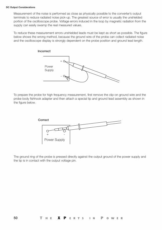
50
DC Output Considerations
Measurement of the noise is performed as close as physically possible to the converter’s outputterminals to reduce radiated noise pick-up. The greatest source of error is usually the unshieldedportion of the oscilloscope probe. Voltage errors induced in the loop by magnetic radiation from thesupply can easily swamp the real measured values.
To reduce these measurement errors unshielded leads must be kept as short as possible. The figurebelow shows the wrong method, because the ground wire of the probe can collect radiated noiseand the oscilloscope display is strongly dependent on the probe position and ground lead length.
PowerSupply
-
+
Power Supply
-+Incorrect
Correct
To prepare the probe for high frequency measurement, first remove the clip-on ground wire and theprobe body fishhook adapter and then attach a special tip and ground lead assembly as shown inthe figure below.
The ground ring of the probe is pressed directly against the output ground of the power supply andthe tip is in contact with the output voltage pin.
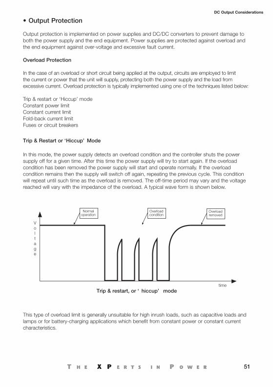
51
DC Output Considerations
• Output Protection
Output protection is implemented on power supplies and DC/DC converters to prevent damage toboth the power supply and the end equipment. Power supplies are protected against overload andthe end equipment against over-voltage and excessive fault current.
Overload Protection
In the case of an overload or short circuit being applied at the output, circuits are employed to limitthe current or power that the unit will supply, protecting both the power supply and the load fromexcessive current. Overload protection is typically implemented using one of the techniques listed below:
Trip & restart or ‘Hiccup’ modeConstant power limitConstant current limitFold-back current limitFuses or circuit breakers
time
Voltage
Normaloperation
Overloadcondition
Overloadremoved
Trip & restart, or ‘ hiccup’ mode
Trip & Restart or ‘Hiccup’ Mode
In this mode, the power supply detects an overload condition and the controller shuts the powersupply off for a given time. After this time the power supply will try to start again. If the overloadcondition has been removed the power supply will start and operate normally. If the overloadcondition remains then the supply will switch off again, repeating the previous cycle. This conditionwill repeat until such time as the overload is removed. The off-time period may vary and the voltagereached will vary with the impedance of the overload. A typical wave form is shown below.
This type of overload limit is generally unsuitable for high inrush loads, such as capacitive loads andlamps or for battery-charging applications which benefit from constant power or constant currentcharacteristics.
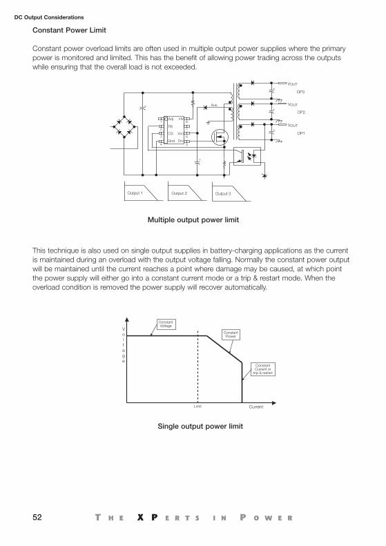
52
DC Output Considerations
Constant Power Limit
Constant power overload limits are often used in multiple output power supplies where the primarypower is monitored and limited. This has the benefit of allowing power trading across the outputswhile ensuring that the overall load is not exceeded.
This technique is also used on single output supplies in battery-charging applications as the currentis maintained during an overload with the output voltage falling. Normally the constant power outputwill be maintained until the current reaches a point where damage may be caused, at which pointthe power supply will either go into a constant current mode or a trip & restart mode. When theoverload condition is removed the power supply will recover automatically.
Multiple output power limit
Voltage
ConstantVoltage
ConstantPower
CurrentLimit
ConstantCurrent or
trip & restart
Single output power limit
Output 1 Output 2 Output 3
Adj
FB
CS
Gnd
HV
Vcc
Drv
1
2
3
4
8
7
6
5
+
+
+
+
+
VOUT
VOUT
VOUT
Aux.
OP3
OP2
OP1
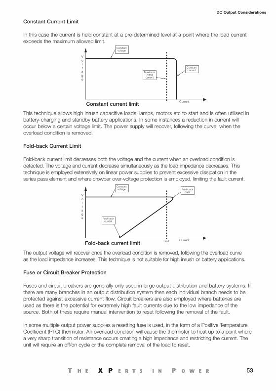
53
DC Output Considerations
This technique allows high inrush capacitive loads, lamps, motors etc to start and is often utilised inbattery-charging and standby battery applications. In some instances a reduction in current willoccur below a certain voltage limit. The power supply will recover, following the curve, when theoverload condition is removed.
Fold-back Current Limit
Fold-back current limit decreases both the voltage and the current when an overload condition isdetected. The voltage and current decrease simultaneously as the load impedance decreases. Thistechnique is employed extensively on linear power supplies to prevent excessive dissipation in theseries pass element and where crowbar over-voltage protection is employed, limiting the fault current.
Current
Voltage
Constantvoltage Fold-back
point
Limit
Fold-backcurrent
Fold-back current limit
Current
Voltage
Constantvoltage
Constantcurrent
Maximumrated
current
Constant Current Limit
In this case the current is held constant at a pre-determined level at a point where the load currentexceeds the maximum allowed limit.
The output voltage will recover once the overload condition is removed, following the overload curveas the load impedance increases. This technique is not suitable for high inrush or battery applications.
Fuse or Circuit Breaker Protection
Fuses and circuit breakers are generally only used in large output distribution and battery systems. Ifthere are many branches in an output distribution system then each individual branch needs to beprotected against excessive current flow. Circuit breakers are also employed where batteries areused as there is the potential for extremely high fault currents due to the low impedance of thesource. Both of these require manual intervention to reset following the removal of the fault.
In some multiple output power supplies a resetting fuse is used, in the form of a Positive TemperatureCoefficient (PTC) thermistor. An overload condition will cause the thermistor to heat up to a point wherea very sharp transition of resistance occurs creating a high impedance and restricting the current. Theunit will require an off/on cycle or the complete removal of the load to reset.
Constant current limit
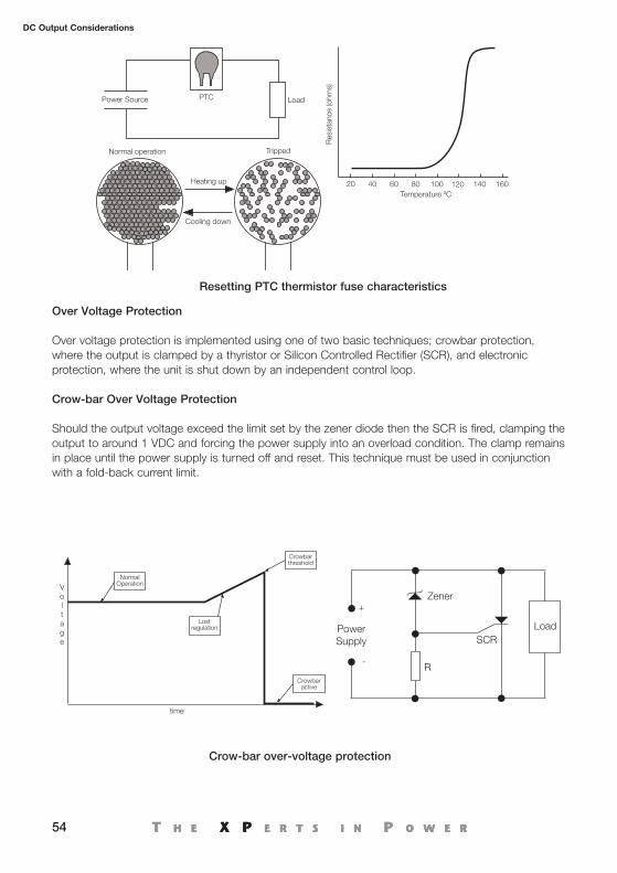
54
DC Output Considerations
Over Voltage Protection
Over voltage protection is implemented using one of two basic techniques; crowbar protection,where the output is clamped by a thyristor or Silicon Controlled Rectifier (SCR), and electronicprotection, where the unit is shut down by an independent control loop.
Crow-bar Over Voltage Protection
Should the output voltage exceed the limit set by the zener diode then the SCR is fired, clamping theoutput to around 1 VDC and forcing the power supply into an overload condition. The clamp remainsin place until the power supply is turned off and reset. This technique must be used in conjunctionwith a fold-back current limit.
Heating up
Cooling down
Normal operation Tripped
LoadPower Source PTC
20 40 60 80 100 120 140 160Temperature ºC
Res
ista
nce
(ohm
s)
Resetting PTC thermistor fuse characteristics
+
-
Load
Zener
SCRPowerSupply
R
Voltage
time
Crowbarthreshold
Crowbaractive
NormalOperation
Lostregulation
Crow-bar over-voltage protection
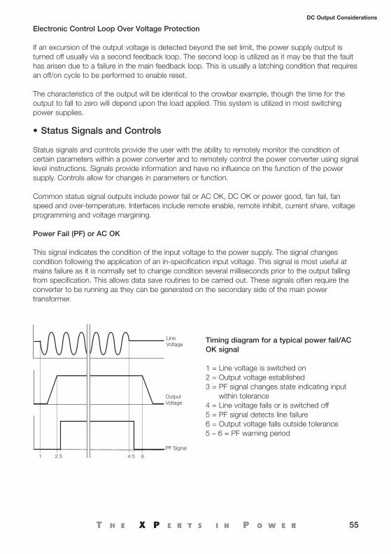
55
DC Output Considerations
Electronic Control Loop Over Voltage Protection
If an excursion of the output voltage is detected beyond the set limit, the power supply output isturned off usually via a second feedback loop. The second loop is utilized as it may be that the faulthas arisen due to a failure in the main feedback loop. This is usually a latching condition that requiresan off/on cycle to be performed to enable reset.
The characteristics of the output will be identical to the crowbar example, though the time for theoutput to fall to zero will depend upon the load applied. This system is utilized in most switchingpower supplies.
• Status Signals and Controls
Status signals and controls provide the user with the ability to remotely monitor the condition ofcertain parameters within a power converter and to remotely control the power converter using signallevel instructions. Signals provide information and have no influence on the function of the powersupply. Controls allow for changes in parameters or function.
Common status signal outputs include power fail or AC OK, DC OK or power good, fan fail, fanspeed and over-temperature. Interfaces include remote enable, remote inhibit, current share, voltageprogramming and voltage margining.
Power Fail (PF) or AC OK
This signal indicates the condition of the input voltage to the power supply. The signal changescondition following the application of an in-specification input voltage. This signal is most useful atmains failure as it is normally set to change condition several milliseconds prior to the output fallingfrom specification. This allows data save routines to be carried out. These signals often require theconverter to be running as they can be generated on the secondary side of the main powertransformer.
LineVoltage
OutputVoltage
PF Signal
1 2 3 4 5 6
Timing diagram for a typical power fail/ACOK signal
1 = Line voltage is switched on2 = Output voltage established3 = PF signal changes state indicating input
within tolerance4 = Line voltage fails or is switched off5 = PF signal detects line failure6 = Output voltage falls outside tolerance5 – 6 = PF warning period
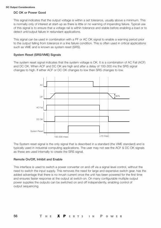
56
DC Output Considerations
DC OK or Power Good
This signal indicates that the output voltage is within a set tolerance, usually above a minimum. Thisis normally only of interest at start-up as there is little or no warning of impending failure. Typical useof this signal is to ensure that a voltage rail is within tolerance and stable before enabling a load or todetect unit/output failure in redundant applications.
This signal can be used in combination with a PF or AC OK signal to enable a warning period priorto the output falling from tolerance in a line failure condition. This is often used in critical applicationssuch as VME and is known as system reset (SRS).
System Reset (SRS/VME) Signals
The system reset signal indicates that the system voltage is OK. It is a combination of AC Fail (ACF)and DC OK. When ACF and DC OK are high and after a delay of 100-300 ms the SRS signalchanges to high. If either ACF or DC OK changes to low then SRS changes to low.
System Reset
100-300 msec >10 msec
DC OK
AC Fail
OP
AC
90%
The System reset signal is the only signal that is described in a standard (the VME standard) and istypically used in industrial computing applications. The user may not see the ACF & DC OK signalsas these are used internally to create the SRS signal.
Remote On/Off, Inhibit and Enable
This interface is used to switch a power converter on and off via a signal level control, without theneed to switch the input supply. This removes the need for large and expensive switch gear, has theadded advantage that there is no inrush current once the unit has been powered for the first timeand ensures faster response at the output at switch-on. On many configurable multiple outputpower supplies the outputs can be switched on and off independently, enabling control ofoutput sequencing.
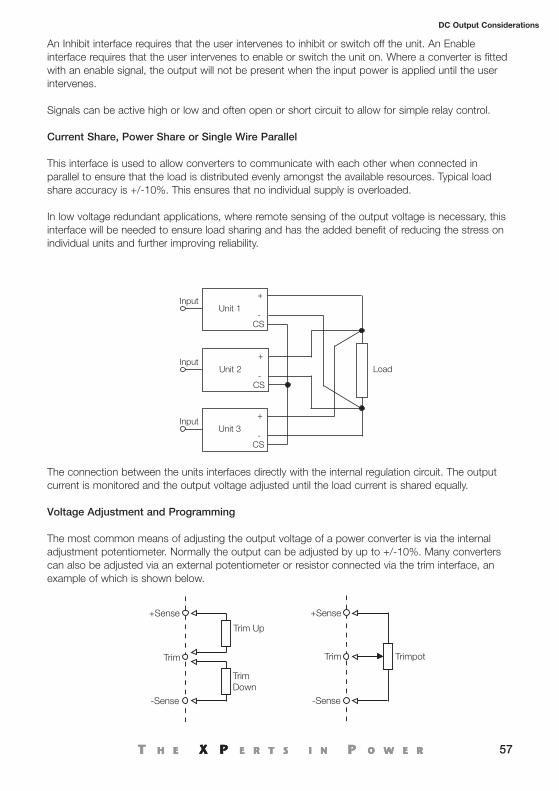
57
DC Output Considerations
An Inhibit interface requires that the user intervenes to inhibit or switch off the unit. An Enableinterface requires that the user intervenes to enable or switch the unit on. Where a converter is fittedwith an enable signal, the output will not be present when the input power is applied until the userintervenes.
Signals can be active high or low and often open or short circuit to allow for simple relay control.
Current Share, Power Share or Single Wire Parallel
This interface is used to allow converters to communicate with each other when connected inparallel to ensure that the load is distributed evenly amongst the available resources. Typical loadshare accuracy is +/-10%. This ensures that no individual supply is overloaded.
In low voltage redundant applications, where remote sensing of the output voltage is necessary, thisinterface will be needed to ensure load sharing and has the added benefit of reducing the stress onindividual units and further improving reliability.
Unit 1
+
-CS
Unit 2
+
-CS
Unit 3
+
-CS
Input
Input
Input
Load
The connection between the units interfaces directly with the internal regulation circuit. The outputcurrent is monitored and the output voltage adjusted until the load current is shared equally.
Voltage Adjustment and Programming
The most common means of adjusting the output voltage of a power converter is via the internaladjustment potentiometer. Normally the output can be adjusted by up to +/-10%. Many converterscan also be adjusted via an external potentiometer or resistor connected via the trim interface, anexample of which is shown below.
Trim Up
TrimDown
Trim
+Sense
-Sense
+Sense
-Sense
Trim Trimpot
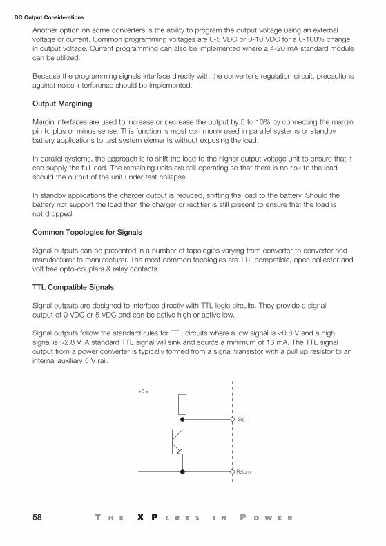
58
DC Output Considerations
Another option on some converters is the ability to program the output voltage using an externalvoltage or current. Common programming voltages are 0-5 VDC or 0-10 VDC for a 0-100% changein output voltage. Current programming can also be implemented where a 4-20 mA standard modulecan be utilized.
Because the programming signals interface directly with the converter’s regulation circuit, precautionsagainst noise interference should be implemented.
Output Margining
Margin interfaces are used to increase or decrease the output by 5 to 10% by connecting the marginpin to plus or minus sense. This function is most commonly used in parallel systems or standbybattery applications to test system elements without exposing the load.
In parallel systems, the approach is to shift the load to the higher output voltage unit to ensure that itcan supply the full load. The remaining units are still operating so that there is no risk to the loadshould the output of the unit under test collapse.
In standby applications the charger output is reduced, shifting the load to the battery. Should thebattery not support the load then the charger or rectifier is still present to ensure that the load isnot dropped.
Common Topologies for Signals
Signal outputs can be presented in a number of topologies varying from converter to converter andmanufacturer to manufacturer. The most common topologies are TTL compatible, open collector andvolt free opto-couplers & relay contacts.
TTL Compatible Signals
Signal outputs are designed to interface directly with TTL logic circuits. They provide a signaloutput of 0 VDC or 5 VDC and can be active high or active low.
Signal outputs follow the standard rules for TTL circuits where a low signal is <0.8 V and a highsignal is >2.8 V. A standard TTL signal will sink and source a minimum of 16 mA. The TTL signaloutput from a power converter is typically formed from a signal transistor with a pull up resistor to aninternal auxiliary 5 V rail.
Sig
Return
+5 V
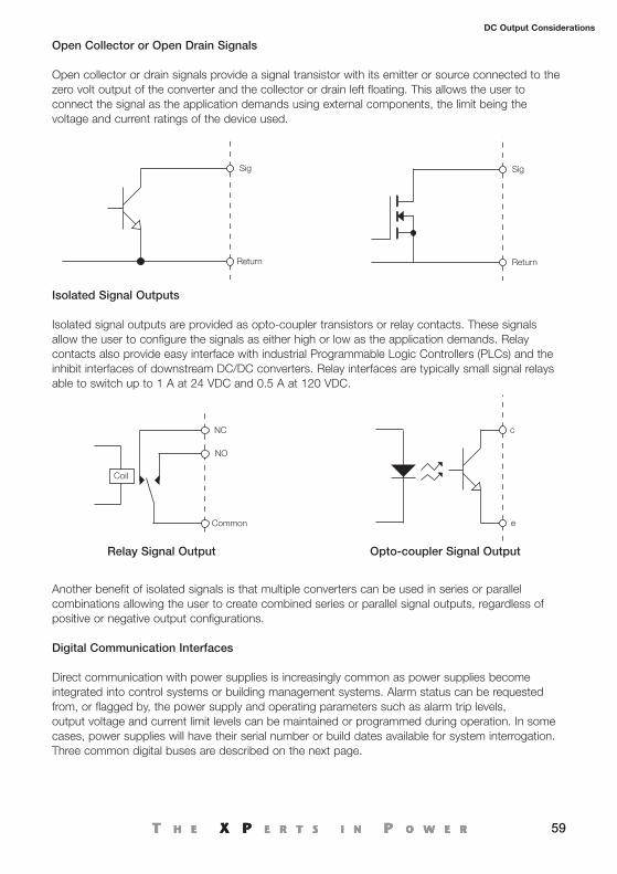
59
DC Output Considerations
Open Collector or Open Drain Signals
Open collector or drain signals provide a signal transistor with its emitter or source connected to thezero volt output of the converter and the collector or drain left floating. This allows the user toconnect the signal as the application demands using external components, the limit being thevoltage and current ratings of the device used.
Isolated Signal Outputs
Isolated signal outputs are provided as opto-coupler transistors or relay contacts. These signalsallow the user to configure the signals as either high or low as the application demands. Relaycontacts also provide easy interface with industrial Programmable Logic Controllers (PLCs) and theinhibit interfaces of downstream DC/DC converters. Relay interfaces are typically small signal relaysable to switch up to 1 A at 24 VDC and 0.5 A at 120 VDC.
Another benefit of isolated signals is that multiple converters can be used in series or parallelcombinations allowing the user to create combined series or parallel signal outputs, regardless ofpositive or negative output configurations.
Digital Communication Interfaces
Direct communication with power supplies is increasingly common as power supplies becomeintegrated into control systems or building management systems. Alarm status can be requestedfrom, or flagged by, the power supply and operating parameters such as alarm trip levels,output voltage and current limit levels can be maintained or programmed during operation. In somecases, power supplies will have their serial number or build dates available for system interrogation.Three common digital buses are described on the next page.
Sig
Return Return
Sig
NC
Common
NO
Coil
c c
e
Relay Signal Output Opto-coupler Signal Output
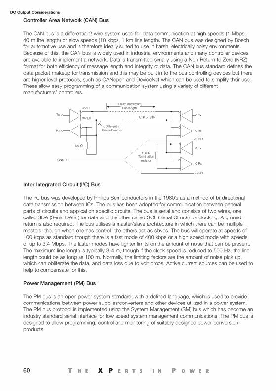
60
DC Output Considerations
Controller Area Network (CAN) Bus
The CAN bus is a differential 2 wire system used for data communication at high speeds (1 Mbps,40 m line length) or slow speeds (10 kbps, 1 km line length). The CAN bus was designed by Boschfor automotive use and is therefore ideally suited to use in harsh, electrically noisy environments.Because of this, the CAN bus is widely used in industrial environments and many controller devicesare available to implement a network. Data is transmitted serially using a Non-Return to Zero (NRZ)format for both efficiency of message length and integrity of data. The CAN bus standard defines thedata packet makeup for transmission and this may be built in to the bus controlling devices but thereare higher level protocols, such as CANopen and DeviceNet which can be used to simplify their use.These allow easy programming of a communication system using a variety of differentmanufacturers’ controllers.
Inter Integrated Circuit (I2C) Bus
The I2C bus was developed by Philips Semiconductors in the 1980’s as a method of bi-directionaldata transmission between ICs. The bus has been adopted for communication between generalparts of circuits and application specific circuits. The bus is serial and consists of two wires, onecalled SDA (Serial DAta ) for data and the other called SCL (Serial CLock) for clocking. A groundreturn is also required. The bus utilises a master/slave architecture in which there can be multiplemasters, though when one has control, the others act as slaves. The bus will operate at speeds of100 kbps as standard though there is a fast mode of 400 kbps or a high speed mode with speedsof up to 3.4 Mbps. The faster modes have tighter limits on the amount of noise that can be present.The maximum line length is typically 3-4 m, though if the clock speed is reduced to 500 Hz, the linelength could be as long as 100 m. Normally, the limiting factors are the amount of noise pick up,which can obliterate the data, and data loss due to volt drops. Active current sources can be used tohelp to compensate for this.
Power Management (PM) Bus
The PM bus is an open power system standard, with a defined language, which is used to providecommunications between power supplies/converters and other devices utilized in a power system.The PM bus protocol is implemented using the System Management (SM) bus which has become anindustry standard serial interface for low speed system management communications. The PM bus isdesigned to allow programming, control and monitoring of suitably designed power conversionproducts.
1000m (maximum)Bus length
UTP or STPTx
Rx
GND
Tx
Rx
GND
Tx
Rx
GNDTermination
resistor
120 Ω
120 Ω
CAN_L
CAN_H
DifferentialDriver/Receiver
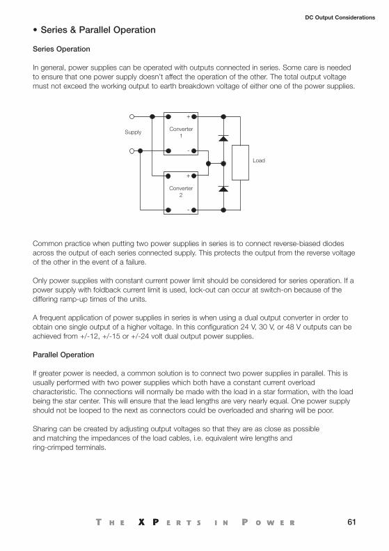
61
DC Output Considerations
• Series & Parallel Operation
Series Operation
In general, power supplies can be operated with outputs connected in series. Some care is neededto ensure that one power supply doesn’t affect the operation of the other. The total output voltagemust not exceed the working output to earth breakdown voltage of either one of the power supplies.
Common practice when putting two power supplies in series is to connect reverse-biased diodesacross the output of each series connected supply. This protects the output from the reverse voltageof the other in the event of a failure.
Only power supplies with constant current power limit should be considered for series operation. If apower supply with foldback current limit is used, lock-out can occur at switch-on because of thediffering ramp-up times of the units.
A frequent application of power supplies in series is when using a dual output converter in order toobtain one single output of a higher voltage. In this configuration 24 V, 30 V, or 48 V outputs can beachieved from +/-12, +/-15 or +/-24 volt dual output power supplies.
Parallel Operation
If greater power is needed, a common solution is to connect two power supplies in parallel. This isusually performed with two power supplies which both have a constant current overloadcharacteristic. The connections will normally be made with the load in a star formation, with the loadbeing the star center. This will ensure that the lead lengths are very nearly equal. One power supplyshould not be looped to the next as connectors could be overloaded and sharing will be poor.
Sharing can be created by adjusting output voltages so that they are as close as possibleand matching the impedances of the load cables, i.e. equivalent wire lengths andring-crimped terminals.
Converter2
+
-
Converter1
+
-
Supply
Load
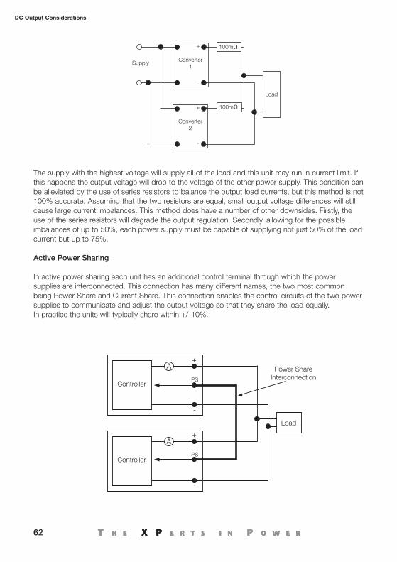
62
DC Output Considerations
The supply with the highest voltage will supply all of the load and this unit may run in current limit. Ifthis happens the output voltage will drop to the voltage of the other power supply. This condition canbe alleviated by the use of series resistors to balance the output load currents, but this method is not100% accurate. Assuming that the two resistors are equal, small output voltage differences will stillcause large current imbalances. This method does have a number of other downsides. Firstly, theuse of the series resistors will degrade the output regulation. Secondly, allowing for the possibleimbalances of up to 50%, each power supply must be capable of supplying not just 50% of the loadcurrent but up to 75%.
Active Power Sharing
In active power sharing each unit has an additional control terminal through which the powersupplies are interconnected. This connection has many different names, the two most commonbeing Power Share and Current Share. This connection enables the control circuits of the two powersupplies to communicate and adjust the output voltage so that they share the load equally.In practice the units will typically share within +/-10%.
Converter2
+
-
Converter1
+
-
Supply
Load
100mΩ
100mΩ
Power Share Interconnection
Controller
Load
+
Controller
A
A
PS
-
+
PS
-
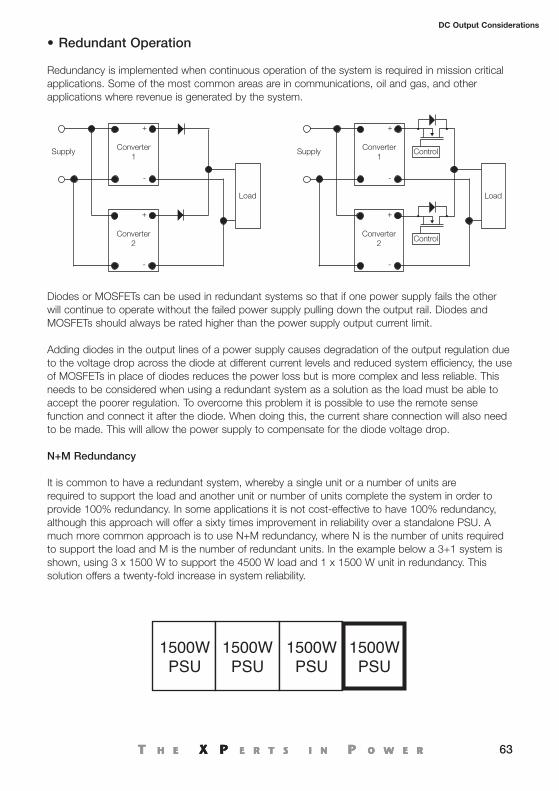
63
DC Output Considerations
• Redundant Operation
Redundancy is implemented when continuous operation of the system is required in mission criticalapplications. Some of the most common areas are in communications, oil and gas, and otherapplications where revenue is generated by the system.
Diodes or MOSFETs can be used in redundant systems so that if one power supply fails the otherwill continue to operate without the failed power supply pulling down the output rail. Diodes andMOSFETs should always be rated higher than the power supply output current limit.
Adding diodes in the output lines of a power supply causes degradation of the output regulation dueto the voltage drop across the diode at different current levels and reduced system efficiency, the useof MOSFETs in place of diodes reduces the power loss but is more complex and less reliable. Thisneeds to be considered when using a redundant system as a solution as the load must be able toaccept the poorer regulation. To overcome this problem it is possible to use the remote sensefunction and connect it after the diode. When doing this, the current share connection will also needto be made. This will allow the power supply to compensate for the diode voltage drop.
N+M Redundancy
It is common to have a redundant system, whereby a single unit or a number of units arerequired to support the load and another unit or number of units complete the system in order toprovide 100% redundancy. In some applications it is not cost-effective to have 100% redundancy,although this approach will offer a sixty times improvement in reliability over a standalone PSU. Amuch more common approach is to use N+M redundancy, where N is the number of units requiredto support the load and M is the number of redundant units. In the example below a 3+1 system isshown, using 3 x 1500 W to support the 4500 W load and 1 x 1500 W unit in redundancy. Thissolution offers a twenty-fold increase in system reliability.
Converter2
+
-
Converter1
+
-
Supply
Load
Converter2
+
-
Converter1
Control
Control
+
-
Supply
Load
1500WPSU
1500WPSU
1500WPSU
1500WPSU
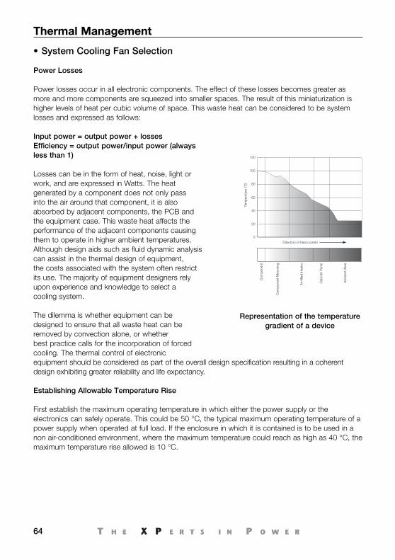
64
Thermal Management
• System Cooling Fan Selection
Power Losses
Power losses occur in all electronic components. The effect of these losses becomes greater asmore and more components are squeezed into smaller spaces. The result of this miniaturization ishigher levels of heat per cubic volume of space. This waste heat can be considered to be systemlosses and expressed as follows:
Input power = output power + lossesEfficiency = output power/input power (alwaysless than 1)
Losses can be in the form of heat, noise, light orwork, and are expressed in Watts. The heatgenerated by a component does not only passinto the air around that component, it is alsoabsorbed by adjacent components, the PCB andthe equipment case. This waste heat affects theperformance of the adjacent components causingthem to operate in higher ambient temperatures.Although design aids such as fluid dynamic analysis can assist in the thermal design of equipment, the costs associated with the system often restrict its use. The majority of equipment designers rely upon experience and knowledge to select a cooling system.
The dilemma is whether equipment can be designed to ensure that all waste heat can be removed by convection alone, or whetherbest practice calls for the incorporation of forcedcooling. The thermal control of electronicequipment should be considered as part of the overall design specification resulting in a coherentdesign exhibiting greater reliability and life expectancy.
Establishing Allowable Temperature Rise
First establish the maximum operating temperature in which either the power supply or theelectronics can safely operate. This could be 50 °C, the typical maximum operating temperature of apower supply when operated at full load. If the enclosure in which it is contained is to be used in anon air-conditioned environment, where the maximum temperature could reach as high as 40 °C, themaximum temperature rise allowed is 10 °C.
Com
pone
nt
Com
pone
nt M
ount
ing
Air-
fille
d In
terio
r
Cab
inet
Pan
el
Am
bien
t Are
a
0
20
40
60
80
100
120
Tem
pera
ture
(˚C
)Direction of heat current
Representation of the temperaturegradient of a device
Thermal_150210.qxp:Layout 1 21/6/10 09:44 Page 64
65
Thermal Management
Establish Power to be Dissipated
If the application has all the load within the equipment then the total power dissipated within theenclosure is the power dissipated by the load and the power dissipated by the power supply due toits inefficiency. Below is an example for a 260 W load supplied by an 85% efficient power supply.
The load power is 260 W+
The power lost due to the inefficiency of the power supply,which is 85% efficient, so the power lost is 46 W
Total power to be dissipated is 306 W
The airflow needed through a system can be calculated as follows:
Where Tc is the allowable temperature rise of the air in the equipment in °C, calculated as themaximum air temperature required minus the maximum temperature of air coming into theequipment (the ambient temperature). Airflow is measured in m3/hr, and the power in Watts is theamount of heat dissipated into the box.
The power supply often has its flow rate given as a linear figure, while fan manufacturers typicallyspecify a volumetric flow rate. To convert from one to the other, convert the volumetric flow rate inm3/hr to m3/s (divide by 3600), then divide the resultant figure by the active area of the fan. Theactive area of the fan is the area traced by the tips of the blades minus the area of the central hub(which is not directly contributing to air movement).
Therefore in our example:
To convert m3/hr to cubic feet per minute (CFM) multiply by 0.589.
Air flow (m3/hr) = 2.6 x Power (W)Tc
Linear flow rate (m/s) = Volumetric flow rate (m3/s)Active fan area (m2)
Air flow (m3/hr) = 2.6 x total power dissipated (W)Allowable temp rise (˚C)
= 2.6 x 306 W10 ˚C
= 79.56 m3/hr (46.86 CFM)
Thermal_150210.qxp:Layout 1 21/6/10 09:44 Page 65
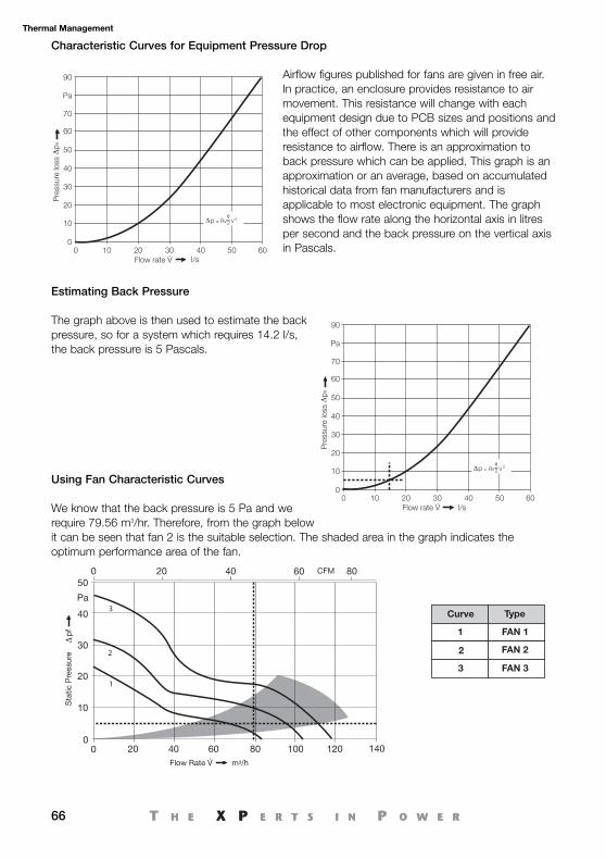
66
Thermal Management
Characteristic Curves for Equipment Pressure Drop
Airflow figures published for fans are given in free air.In practice, an enclosure provides resistance to airmovement. This resistance will change with eachequipment design due to PCB sizes and positions andthe effect of other components which will provideresistance to airflow. There is an approximation toback pressure which can be applied. This graph is anapproximation or an average, based on accumulatedhistorical data from fan manufacturers and isapplicable to most electronic equipment. The graphshows the flow rate along the horizontal axis in litresper second and the back pressure on the vertical axisin Pascals.
Estimating Back Pressure
The graph above is then used to estimate the backpressure, so for a system which requires 14.2 l/s, the back pressure is 5 Pascals.
Using Fan Characteristic Curves
We know that the back pressure is 5 Pa and werequire 79.56 m3/hr. Therefore, from the graph belowit can be seen that fan 2 is the suitable selection. The shaded area in the graph indicates theoptimum performance area of the fan.
90
70
Pa
60
50
40
30
20
10
00 10 20 30 40 50 60
l/sFlow rate V
Pre
ssur
e lo
ss
pv
p = Rv V 22
90
70
Pa
60
50
40
30
20
10
00 10 20 30 40 50 60
l/sFlow rate V
Pre
ssur
e lo
ss
pv
p = Rv V 22
3
2
1
0
00
20
20 40 60 80 100 120
4050
Pa
40
30
20
10
CFM
Sta
tic P
ress
ure
pf
m3/hFlow Rate V
60 80
140
Curve Type
1
2
3
FAN 1
FAN 2
FAN 3
Thermal_150210.qxp:Layout 1 21/6/10 09:44 Page 66
67
Thermal Management
• Cooling Power Supplies
Power supplies generate waste heat which has to be dissipated. They typically have eitherconvection cooled or forced cooled ratings or, in some cases, both. Forced cooled power suppliesmay incorporate a cooling fan, or may specify the user cooling required to operate the unit atmaximum load and ambient temperature.
Where user cooling is required it is most important that the power supply cooling is adequate forboth safe operation and adequate service life. It is very application specific and dependent on theambient temperature, applied load and physical location with respect to the cooling fan and othersystem assemblies.
The main difference between convection and force cooled products is in the power density offered.For a given efficiency, convection cooled products offer a lower power density, meaning that theyoccupy a larger volume. A power supply on a 3” x 5” industry standard footprint may have aconvection rating of 150 W while the force cooled version may have a rating as high as 350 W.
Convection Cooling
Where the power supply has a convection cooled rating, it is intended to be used in an environmentwhere there is free air. The system designer must ensure that there is adequate space around andabove the unit for free air convection currents to cool the unit and must also ensure that the ambienttemperature local to the power supply is controlled to a level within its maximum ratings.
Forced Cooling
Force cooled products with integral cooling fans are easy to apply as it is a simple matter of ensuringthat the maximum specified ambient temperature is not exceeded for a given load rating and that theintake and exhaust areas are not obstructed.
Typically, power supplies that require the user to provide forced air cooling will specify a minimumrequired airflow. This is usually for operation at 100% of the power rating at the maximum ambienttemperature allowed.
The required airflow is often specified in Cubic Feet per Minute (CFM) which is also the commonrating for cooling fans. The effectiveness of cooling fans installed in enclosures must be givenconsideration, as discussed earlier in this section, and the CFM rating deals in volume of air ratherthan air speed, which is the important factor. The object is to maintain the components used withinthe power supply at a safe operating temperature and to ensure adequate service life.
When the required airflow is specified in CFM it assumes that the power supply is installed in an areawhich is relatively similar to it’s own cross sectional area. This is rarely the case as the power supplyis typically used as a sub-assembly within a complete equipment enclosure. It will also assume thatthe air is directed at the power supply, which may also not be the case, so converting to Linear Feetper Minute (LFM) or meters per second (m/s) provides a more valid criterion as linear air speedmeasurements specify where the air is flowing and directly relate to heat transfer.
Thermal_150210.qxp:Layout 1 21/6/10 09:44 Page 67
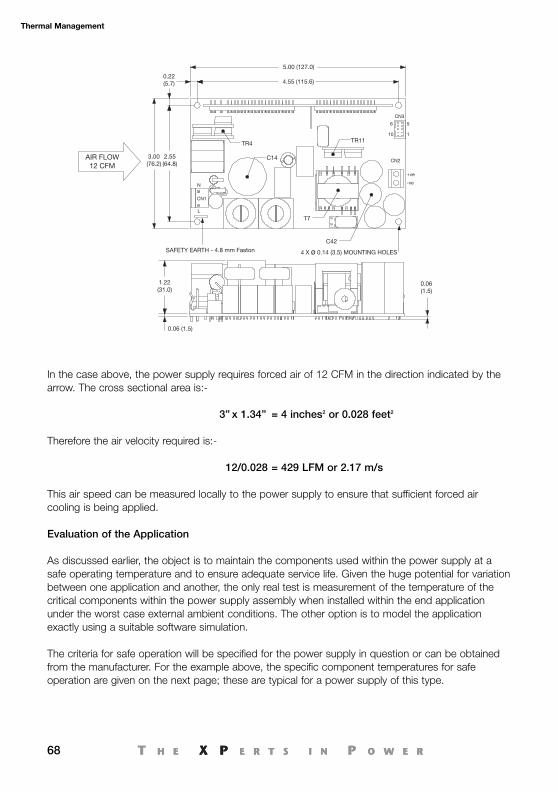
68
Thermal Management
In the case above, the power supply requires forced air of 12 CFM in the direction indicated by thearrow. The cross sectional area is:-
3” x 1.34” = 4 inches2 or 0.028 feet2
Therefore the air velocity required is:-
12/0.028 = 429 LFM or 2.17 m/s
This air speed can be measured locally to the power supply to ensure that sufficient forced aircooling is being applied.
Evaluation of the Application
As discussed earlier, the object is to maintain the components used within the power supply at asafe operating temperature and to ensure adequate service life. Given the huge potential for variationbetween one application and another, the only real test is measurement of the temperature of thecritical components within the power supply assembly when installed within the end applicationunder the worst case external ambient conditions. The other option is to model the applicationexactly using a suitable software simulation.
The criteria for safe operation will be specified for the power supply in question or can be obtainedfrom the manufacturer. For the example above, the specific component temperatures for safeoperation are given on the next page; these are typical for a power supply of this type.
AIR FLOW12 CFM
5.00 (127.0)
4 X ø 0.14 (3.5) MOUNTING HOLESSAFETY EARTH - 4.8 mm Faston
4.55 (115.6)0.22(5.7)
CN1
CN3
1
5
10
6
CN2
+ve
-veN
L
2.55(64.8)
3.00(76.2)
1.22(31.0)
0.06(1.5)
0.06 (1.5)
TR4
T7
C42
C14
TR11
Thermal_150210.qxp:Layout 1 21/6/10 09:44 Page 68
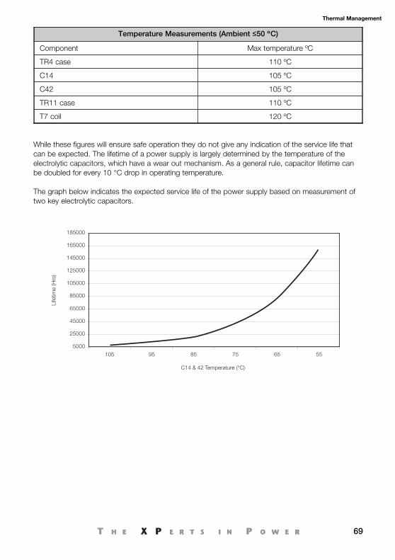
69
Thermal Management
While these figures will ensure safe operation they do not give any indication of the service life thatcan be expected. The lifetime of a power supply is largely determined by the temperature of theelectrolytic capacitors, which have a wear out mechanism. As a general rule, capacitor lifetime canbe doubled for every 10 °C drop in operating temperature.
The graph below indicates the expected service life of the power supply based on measurement oftwo key electrolytic capacitors.
Temperature Measurements (Ambient ≤50 ºC)
Component Max temperature ºC
TR4 case 110 ºC
C14 105 ºC
C42 105 ºC
TR11 case 110 ºC
T7 coil 120 ºC
5000
25000
45000
65000
85000
105000
125000
145000
165000
185000
105 95 85 75 65
C14 & 42 Temperature (°C)
Life
time
(Hrs
)
55
Thermal_150210.qxp:Layout 1 21/6/10 09:44 Page 69
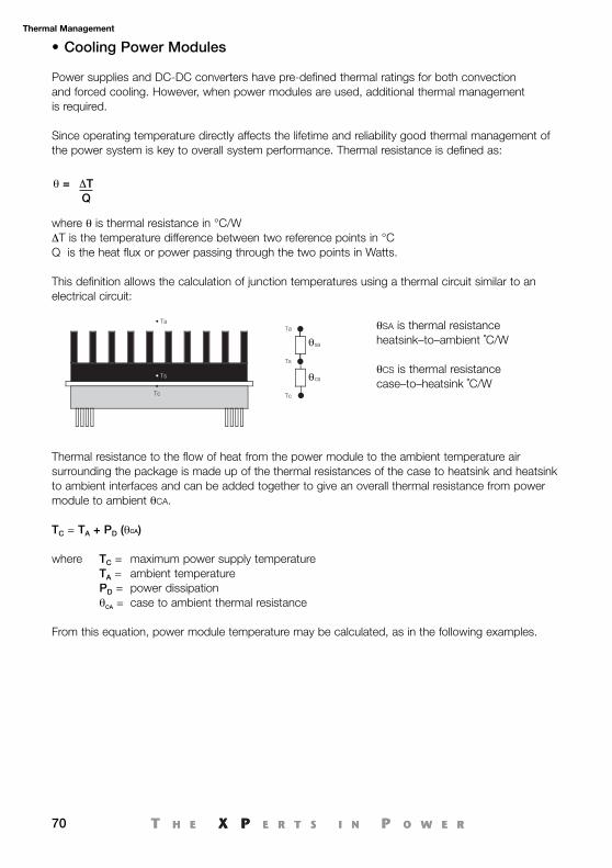
70
Thermal Management
• Cooling Power Modules
Power supplies and DC-DC converters have pre-defined thermal ratings for both convectionand forced cooling. However, when power modules are used, additional thermal management is required.
Since operating temperature directly affects the lifetime and reliability good thermal management ofthe power system is key to overall system performance. Thermal resistance is defined as:
where θ is thermal resistance in °C/W ΔT is the temperature difference between two reference points in °CQ is the heat flux or power passing through the two points in Watts.
This definition allows the calculation of junction temperatures using a thermal circuit similar to anelectrical circuit:
θSA is thermal resistanceheatsink–to–ambient ˚C/W
θCS is thermal resistancecase–to–heatsink ˚C/W
Thermal resistance to the flow of heat from the power module to the ambient temperature airsurrounding the package is made up of the thermal resistances of the case to heatsink and heatsinkto ambient interfaces and can be added together to give an overall thermal resistance from powermodule to ambient θCA.
TC = TA + PD (θCA)
where TC = maximum power supply temperatureTA = ambient temperaturePD = power dissipationθCA = case to ambient thermal resistance
From this equation, power module temperature may be calculated, as in the following examples.
• TaTa
sa
Ts
Tc
•Tc
• Ts cs
θ = ΔTQ
Thermal_150210.qxp:Layout 1 21/6/10 09:44 Page 70
71
Thermal Management
Example: A power module package must operate in ambient temperature of +30 ˚C. What is its baseplate temperature? Let PD = 5 W and θCA = 11.0 ˚C/W.
TC = TA + PD θCA = 30 + (5 x 11.0) = +85.0 ˚C
Example: Assume that a heatsink is used giving a θCA of 3.0 ˚C/W. Using thisheatsink the above example would result in a baseplate temperature given by:
TC = TA + PD θCA = 50 + (5 x 3.0) = +65.0 ˚C
Example: The same device to be used at an ambient temperature of +50 ˚C, what is its case temperature?
TC = TA + PD θCA = 50 + (5 x 11.0) = +105.0 ˚C
Where operation in a higher ambient temperature is necessary, the maximum power moduletemperature can easily be exceeded unless suitable measures are taken.
This exceeds most power module maximum operating temperatures and therefore some means ofdecreasing the case–to–ambient thermal resistance is required.
As stated earlier, θCA is the sum of the individual thermal resistances; of these, θcs is fixed by thedesign of device and package and so only the case–to–ambient thermal resistance, θCA, can be reduced.
If θCA, and therefore θJA, is reduced by the use of a suitable heatsink, then the maximum Tamb can be increased:
These calculations are not an exact science because factors such as θCA may vary from device type todevice type and the efficacy of the heatsink may vary according to the air movement in the equipment.
Where it is impossible to improve the dissipation capability of the heatsink, forced air coolingbecomes necessary and, though the simple approach outlined above is useful, more factors must betaken into account when forced air cooling is implemented.
• Baseplate Cooling
The use of power supplies in harsh or remote environments brings many fundamental designissues that must be fully understood if long-term reliability is to be attained.
Under these conditions, it is generally accepted that electronic systems must be sealed againstthe elements making the removal of unwanted heat particularly difficult. The use of forced-aircooling is undesirable as it increases system size, adds the maintenance issues of cleaning orreplacing filters and introduces a wear out mechanism in the fan.
A commonly adopted solution is to use a standard power supply and modify the mechanical designto enable removal of heat from the sealed system. This simple compromise does not really addressthe fundamental issues of power supply design for the applications described and a more practical approach is to select a power supply which has been designed specifically for sealed enclosure applications.
Thermal_150210.qxp:Layout 1 21/6/10 09:44 Page 71
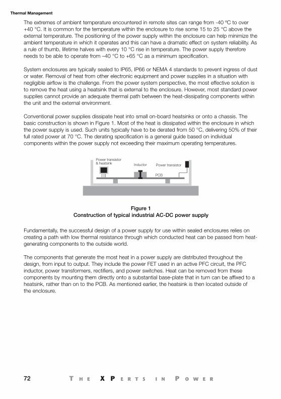
72
Thermal Management
The extremes of ambient temperature encountered in remote sites can range from -40 ºC to over+40 °C. It is common for the temperature within the enclosure to rise some 15 to 25 °C above theexternal temperature. The positioning of the power supply within the enclosure can help minimize theambient temperature in which it operates and this can have a dramatic effect on system reliability. Asa rule of thumb, lifetime halves with every 10 °C rise in temperature. The power supply thereforeneeds to be able to operate from –40 °C to +65 °C as a minimum specification.
System enclosures are typically sealed to IP65, IP66 or NEMA 4 standards to prevent ingress of dustor water. Removal of heat from other electronic equipment and power supplies in a situation withnegligible airflow is the challenge. From the power system perspective, the most effective solution isto remove the heat using a heatsink that is external to the enclosure. However, most standard powersupplies cannot provide an adequate thermal path between the heat-dissipating components withinthe unit and the external environment.
Conventional power supplies dissipate heat into small on-board heatsinks or onto a chassis. Thebasic construction is shown in Figure 1. Most of the heat is dissipated within the enclosure in whichthe power supply is used. Such units typically have to be derated from 50 °C, delivering 50% of theirfull rated power at 70 °C. The derating specification is a general guide based on individualcomponents within the power supply not exceeding their maximum operating temperatures.
Fundamentally, the successful design of a power supply for use within sealed enclosures relies oncreating a path with low thermal resistance through which conducted heat can be passed from heat-generating components to the outside world.
The components that generate the most heat in a power supply are distributed throughout thedesign, from input to output. They include the power FET used in an active PFC circuit, the PFCinductor, power transformers, rectifiers, and power switches. Heat can be removed from thesecomponents by mounting them directly onto a substantial base-plate that in turn can be affixed to aheatsink, rather than on to the PCB. As mentioned earlier, the heatsink is then located outside of the enclosure.
PCB
Power transistor& heatsink Power transistorInductor
Figure 1 Construction of typical industrial AC-DC power supply
Thermal_150210.qxp:Layout 1 21/6/10 09:44 Page 72
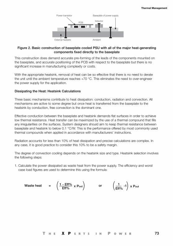
73
Thermal Management
This construction does demand accurate pre-forming of the leads of the components mounted onthe baseplate, and accurate positioning of the PCB with respect to the baseplate but there is nosignificant increase in manufacturing complexity or costs.
With the appropriate heatsink, removal of heat can be so effective that there is no need to deratethe unit until the ambient temperature reaches +70 °C. This eliminates the need to over-engineerthe power supply for the application.
Dissipating the Heat: Heatsink Calculations
Three basic mechanisms contribute to heat dissipation: conduction, radiation and convection. Allmechanisms are active to some degree but once heat is transferred from the baseplate to theheatsink by conduction, free convection is the dominant one.
Effective conduction between the baseplate and heatsink demands flat surfaces in order to achievelow thermal resistance. Heat transfer can be maximized by the use of a thermal compound that fillsany irregularities on the surfaces. System designers should aim to keep thermal resistance betweenbaseplate and heatsink to below 0.1 °C/W. This is the performance offered by most commonly usedthermal compounds when applied in accordance with manufacturers’ instructions.
Radiation accounts for less than 10% of heat dissipation and precise calculations are complex. Inany case, it is good practice to consider this 10% to be a safety margin.
The degree of convection cooling depends on the heatsink size and type. Heatsink selection involvesthe following steps:
1. Calculate the power dissipated as waste heat from the power supply. The efficiency and worstcase load figures are used to determine this using the formula:
PCB
Power transistor Baseplate of power supply
AmbientExternal heatsink
Inductor
Figure 2. Basic construction of baseplate cooled PSU with all of the major heat-generating components fixed directly to the baseplate
x Pout1 -1 x Pout
Eff%1 - Eff%
Eff%( (( (
Waste heat = or
Thermal_150210.qxp:Layout 1 21/6/10 09:44 Page 73
74
Thermal Management
2. Estimate the resistance of the thermal interface between the power supply baseplate and theheatsink. This is typically 0.1 °C/W when using a thermal compound.
3. Calculate the maximum allowable temperature rise on the baseplate. The allowable temperaturerise is simply:
TB – TA where TA is the maximum ambient temperature outside of the cabinet and TB is the maximum allowable baseplate temperature.
4. The required heatsink is defined by its thermal impedance using the formula:
θH = TB – TA -0.1Waste Power
5. The final choice is then based on the best physical design of heatsink for the application that candeliver the required thermal impedance. The system’s construction will determine the maximumavailable area for contact with the baseplate of the power supply and the available space outsideof the enclosure will then determine the size, number and arrangement of cooling fins on theheatsink to meet the dissipation requirement.
Conclusion
The reliability of remotely-sited electronic equipment is fundamentally dependent upon power supplyreliability. The most cost-effective approach to power system design is to use power suppliesdesigned for the application, which conduct heat via large, flat baseplates to heatsinks that can bemounted outside of the enclosure.
Thermal_150210.qxp:Layout 1 21/6/10 09:44 Page 74
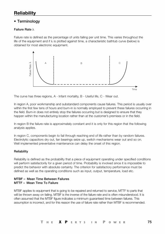
75
Reliability
• Terminology
Failure Rate λ
Failure rate is defined as the percentage of units failing per unit time. This varies throughout thelife of the equipment and if λ is plotted against time, a characteristic bathtub curve (below) isobtained for most electronic equipment.
The curve has three regions, A - Infant mortality, B - Useful life, C - Wear out.
In region A, poor workmanship and substandard components cause failures. This period is usually overwithin the first few tens of hours and burn-in is normally employed to prevent these failures occurring inthe field. Burn-in does not entirely stop the failures occurring but is designed to ensure that theyhappen within the manufacturing location rather than at the customer’s premises or in the field.
In region B the failure rate is approximately constant and it is only for this region that the followinganalysis applies.
In region C, components begin to fail through reaching end of life rather than by random failures.Electrolytic capacitors dry out, fan bearings seize up, switch mechanisms wear out and so on. Well implemented preventative maintenance can delay the onset of this region.
Reliability
Reliability is defined as the probability that a piece of equipment operating under specified conditionswill perform satisfactorily for a given period of time. Probability is involved since it is impossible topredict the behavior with absolute certainty. The criterion for satisfactory performance must bedefined as well as the operating conditions such as input, output, temperature, load etc.
MTBF – Mean Time Between FailuresMTTF – Mean Time To Failure
MTBF applies to equipment that is going to be repaired and returned to service, MTTF to parts thatwill be thrown away on failing. MTBF is the inverse of the failure rate and is often misunderstood. It isoften assumed that the MTBF figure indicates a minimum guaranteed time between failures. Thisassumption is incorrect, and for this reason the use of failure rate rather than MTBF is recommended.
A B C
Failu
re R
ate
Time
Thermal_150210.qxp:Layout 1 21/6/10 09:44 Page 75
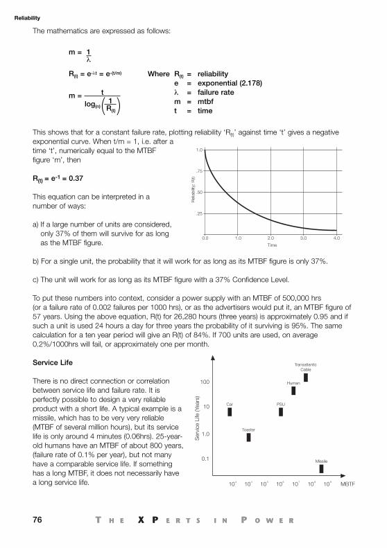
76
Reliability
The mathematics are expressed as follows:
This shows that for a constant failure rate, plotting reliability ‘R(t)’ against time ‘t’ gives a negativeexponential curve. When t/m = 1, i.e. after atime ‘t’, numerically equal to the MTBFfigure ‘m’, then
R(t) = e-1 = 0.37
This equation can be interpreted in anumber of ways:
a) If a large number of units are considered,only 37% of them will survive for as longas the MTBF figure.
b) For a single unit, the probability that it will work for as long as its MTBF figure is only 37%.
c) The unit will work for as long as its MTBF figure with a 37% Confidence Level.
To put these numbers into context, consider a power supply with an MTBF of 500,000 hrs(or a failure rate of 0.002 failures per 1000 hrs), or as the advertisers would put it, an MTBF figure of57 years. Using the above equation, R(t) for 26,280 hours (three years) is approximately 0.95 and ifsuch a unit is used 24 hours a day for three years the probability of it surviving is 95%. The samecalculation for a ten year period will give an R(t) of 84%. If 700 units are used, on average0.2%/1000hrs will fail, or approximately one per month.
Service Life
There is no direct connection or correlationbetween service life and failure rate. It isperfectly possible to design a very reliableproduct with a short life. A typical example is amissile, which has to be very very reliable(MTBF of several million hours), but its servicelife is only around 4 minutes (0.06hrs). 25-year-old humans have an MTBF of about 800 years,(failure rate of 0.1% per year), but not manyhave a comparable service life. If somethinghas a long MTBF, it does not necessarily havea long service life.
1.0
.75
.50
.25
0.0 1.0 2.0 3.0 4.0
Time
Rel
iabi
lity:
R(t)
Ser
vice
Life
(Yea
rs)
MBTF
0.1
1.0
10
100
10 3 10 4 10 5 10 6 10 7 10 8 10 9
Car PSU
Human
Missile
Transatlantic Cable
Toaster
m = 1λ
R(t) = e-λt = e-(t/m)
t
Where R(t) = reliabilitye = exponential (2.178)λ = failure ratem = mtbft = time
log(n) R(t)
1m = ((
Thermal_150210.qxp:Layout 1 21/6/10 09:44 Page 76
77
Reliability
• Factors Affecting Reliability
The most important factor is good, careful design based on sound experience, resulting in knownsafety margins. Unfortunately, this does not show up in any predictions, since they assume aperfect design.
Many field failures of electronic equipment are not due to the classical random failure patterndiscussed here, but to shortcomings in the design and in the application of the components, as wellas external factors such as occasional voltage surges. These may be outside of the specification butno one will ever know as all that will be seen is a failed unit. Making the units rugged through carefuldesign and controlled overstress testing is a very important part of making the product reliable.
The failure rate of the equipment depends on these three factors.
Complexity Keep things simple, because what isn’t there can’t fail but, conversely, what isn’tthere can cause a failure. A complicated or difficult specification will invariably resultin reduced reliability. This is not due to the shortcomings of the design staff, but tothe resultant component count. Every component used will contribute to theequipment's unreliability.
Stress For electronic equipment, the most prominent stresses are temperature, voltage,vibration and temperature rise due to current. The effect of each of these stresseson each of the components must be considered. In order to achieve good reliability,various derating factors have to be applied to these stress levels. The derating hasto be traded off against cost and size implications. Great care and attention to detailis necessary to reduce thermal stresses as far as possible. The layout has to besuch that heat-generating components are kept away from other components andare adequately cooled. Thermal barriers are used where necessary and adequateventilation needs to be provided.
The importance of these provisions cannot be overstressed since the failure rate ofthe components will double for a 10 ºC increase in temperature. Decreasing the sizeof a unit without increasing its efficiency will make it hotter, and therefore less reliable.
Generic Generic reliability (also known as inherent reliability) refers to the fact that, forexample, film capacitors are more reliable than electrolytic capacitors, wirewrapconnections more reliable than soldered ones, fixed resistors more reliable thanpotentiometers. Components have to be carefully selected to avoid the types withhigh generic failure rates. Quite often there is a cost trade-off, as more reliablecomponents can be more expensive.
Thermal_150210.qxp:Layout 1 21/6/10 09:44 Page 77
78
Reliability
Estimating the Failure Rate
The failure rate should be estimated and measured throughout the life of the equipment. During thedesign, it is predicted. During the manufacture, it is assessed. During the service life, it is observed.
The failure rate is predicted by evaluating each of the factors affecting reliability for each componentand then summing these to obtain the failure rate of the whole equipment. It is essential that thedatabase used is defined and used consistently. There are three databases in common use: MIL-HDBK-217, HRD5 and Bellcore. These reflect the experiences of the US Navy, British Telecomand Bell Telephone respectively.
In general, predictions assume that the design is perfect, the stresses known, everything is withinratings at all times, so that only random failures occur; every failure of every part will cause theequipment to fail and that the database is valid. These assumptions are incorrect. The design is lessthan perfect, not every failure of every part will cause the equipment to fail, and the database is likelyto be 15 years out of date. However, none of this matters as long as the predictions are usedto compare different topologies or approaches rather than to establish an absolute figure for reliability.This is what predictions should be used for.
Prediction
Parts stress method In this method, each factor affecting reliability for each component isevaluated. Since the average power supply has over 100 componentsand each component about seven factors (stress ratio, generic,temperature, quality, environment, construction and complexity), thismethod requires considerable effort and time. Predictions are usuallymade in order to compare different approaches of topologies, i.e. whendetailed design information is not available and the design itself is still ina fluid state. Under such circumstances it is hardly worthwhile toexpend this effort and the much simpler and quicker Parts countmethod is used.
Parts count method In this method, all like components are grouped together, and averagefactors allocated for the group. So, for example, instead of working outall the factors for each of the 15 electrolytic capacitors used there isonly one entry of capacitor with a quantity of 15. Usually only twofactors are allocated, generic and quality. The other factors, includingstress levels, are assumed to be at some realistic level and allowed forin the calculation. For this reason, the factors are not interchangeablebetween the two methods. In general, for power supplies, HRD5 givesthe most favourable result closely followed by Bellcore, with MIL-217the least favorable. This depends on the mix of components in theparticular equipment, since one database is ‘unfair’ on ICs, and anotheron FETs. Hence the importance of comparing results from likedatabases only.
Thermal_150210.qxp:Layout 1 21/6/10 09:44 Page 78
79
Reliability
Assessment This is the most useful and accurate way of predicting the failure rate. A number of units are put on life test, at an elevated temperature, andso the stresses and the environment are controlled.
During life tests and reliability demonstration tests it is usual to apply greater stresses than normal, sothat the desired result is obtained more quickly. Great care has to be applied to ensure that theeffects of the extra stress are known and proven to be calculable and that no hidden additionalfailure mechanisms are activated by the extra stress. The usual extra stress is an increase oftemperature and its effect can be calculated as long as the maximum ratings of the device are not exceeded.
Prototype Testing
With all the sophisticated computer analysis available, there is still no substitute for thoroughly testingproducts or components. One way of doing this would be to perform HALT testing. HALT (HighlyAccelerated Life Test) is used to test as many different conditions as possible and cycling thetemperature, input and load independently.
Manufacturing Methods
Suppliers must be strictly controlled and deliver consistently good product with prior warning of anychanges to processes. Because of the supply chain JIT and QA practices this can be achieved bydealing with a small number of trusted suppliers.
Manual assembly is prone to errors and to some random, unintentional abuse of the components byoperators, such as ESD. This causes defects, which will show themselves later.
Changing settings produces inconsistency and side effects. A good motto is ‘if it works leave italone, if it does not, find the root cause.’ There must be a reason for the deviation and this must befound and eliminated, rather than masked by an adjustment.
The results from the HALT test can be used to set test limits for production screening. HighlyAccelerated Stress Screening (HASS) uses the same equipment as for HALT tests but knowing theoperating and destruct (where possible) limits can be used to screen HALT tested products inproduction. This process differs from conventional stress screening in that the climatic andmechanical stimuli are much higher and consequently the test times are much shorter. HASS can besummed up as a process used in manufacturing to allow discovery of process changes and preventproducts with latent defects from getting into the field.
Thermal_150210.qxp:Layout 1 21/6/10 09:44 Page 79
80
Reliability
• System Reliability
There are two further methods of increasing system reliability.
More reliable components MIL standard or other components of assessed quality could be usedbut in industrial and commercial equipment this expense is not normallyjustified.
Redundancy In a system where one unit can support the load and two units are usedin parallel, the system is much more reliable since the system will stillwork if one unit fails. Clearly, the probability of both units failingsimultaneously is much lower than that of one unit failing.
Redundancy has a size and cost penalty so normally an n+1 system is used, where n units can supportthe load, but n+1 units are used in parallel, 2+1 or 3+1 being the usual combinations. Supposing thereliability of each unit under the particular conditions is 0.9826, the system reliability for an n+1 systemwhere n=2 would be 0.9991, an improvement of 20 times. (Nearly 60 times in a 1+1 system).
There are downsides to this approach. More units, higher cost and the need for faulty units to bebrought to the operator’s attention so that they can be replaced, changing units must not make thesystem fail (hot swap). The extra circuitry required to monitor all aspects and ensure reliability in itself increases the failure rate and cost of the system (see page 63 for more details on redundant operation).
Comparing Reliability
When comparing reliability figures, the following points must be satisfied.
• The database must be stated and must be identical. Comparing a MIL-HDBK-217F prediction witha MIL-HDBK-217E prediction or an HRD5 prediction is meaningless as there is no correlation.
• The database must be used consistently and exclusively. The result is meaningless if a differentdatabase is used for some components.
• The external stresses and environment must be stated and be identical. (input, load, temperatureetc). The result is meaningless if all the environmental details are not stated or are different.
• The units must be form-fit function interchangeable. If, for example, the ratings are identical, butone needs an external filter and the other does not then there is no comparison (although youcould work out the failure rate of the filter and add it to the failure rate of the unit).
There is no magic; if one manufacturer predicts 200,000 hours and another states 3,000,000 hoursfor a comparable product, then they must have used a different database, a different stress levelor a different environment.
Thermal_150210.qxp:Layout 1 21/6/10 09:44 Page 80
81
Legislation
• Power Supply Safety
Legislation requires electrical equipment to be designed to reduce the likelihood of injury or damagedue to:
• Electric shock • Energy related hazards• Fire • Heat related hazards• Radiation • Chemical hazards
A safe power supply is an inherent part of any electrical product and must comply with the relevantsafety standard. There are several standards which could be used for power supplies and thedecision on which to use depends on the intended application of the end product.
There is an international product specific standard for power supplies which is used to demonstratecompliance with the safety requirements, this is part of the IEC61204 range of standards. Thestandard covers both stand alone and component power supplies and references the product familystandards IEC60950, IEC60601, IEC61010 & IEC60065.
Most power supplies will use an information technology equipment standard (60950), a medicalequipment standard (60601) or less commonly a standard for equipment used for measurement,control and laboratory use (61010). This latter standard covers equipment intended for professional,industrial process and educational use such as equipment for testing or measuring non-electricalquantities, controlling output quantities to specific values or laboratory equipment which measures,analyses or prepares materials.
Another standard which is sometimes used in conjunction with one of the above is UL508 whichcovers industrial equipment intended to power control systems for electrical motors. It is common forDIN rail power supplies to have approval to this standard.
The standard for information technology equipment, IEC60950, covers a wide range of producttypes and is commonly used. Approvals are separately granted by a number of national testlaboratories depending on the target markets. UL (Underwriters Laboratories, UL60950) arecommonly used for approvals in North America, CSA (Canadian Standards Association, CSA22.2No.60950) for Canada and there are a number of European test laboratories which will grantapproval for EU wide use, EN60950. UL & CSA also operate a scheme to grant approvals for both markets.
In the major Asian markets other approvals are required. The requirements are essentially as laid outin IEC60950 with some additional testing in some instances, including EMC.
China CCC (China Compulsory Certification)Taiwan BSMI (Bureau of Standards, Metrology & Inspection)Japan PSE (Product Safety Electric Appliance & Materials)Korea KETI (Korean Electrical Testing Institute)
There are many other approval bodies in existence which may need to be considered depending onthe equipment target markets.
Legislation_150210.qxp:Layout 1 21/6/10 09:49 Page 81
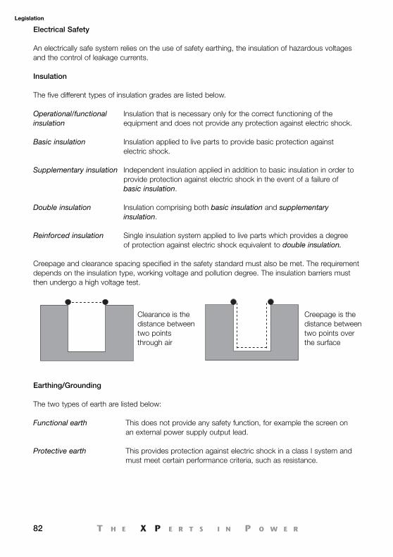
82
Legislation
Electrical Safety
An electrically safe system relies on the use of safety earthing, the insulation of hazardous voltagesand the control of leakage currents.
Insulation
The five different types of insulation grades are listed below.
Operational/functional Insulation that is necessary only for the correct functioning of theinsulation equipment and does not provide any protection against electric shock.
Basic insulation Insulation applied to live parts to provide basic protection againstelectric shock.
Supplementary insulation Independent insulation applied in addition to basic insulation in order toprovide protection against electric shock in the event of a failure ofbasic insulation.
Double insulation Insulation comprising both basic insulation and supplementaryinsulation.
Reinforced insulation Single insulation system applied to live parts which provides a degreeof protection against electric shock equivalent to double insulation.
Creepage and clearance spacing specified in the safety standard must also be met. The requirementdepends on the insulation type, working voltage and pollution degree. The insulation barriers mustthen undergo a high voltage test.
Earthing/Grounding
The two types of earth are listed below:
Functional earth This does not provide any safety function, for example the screen onan external power supply output lead.
Protective earth This provides protection against electric shock in a class I system andmust meet certain performance criteria, such as resistance.
Clearance is thedistance betweentwo pointsthrough air
Creepage is thedistance betweentwo points overthe surface
Legislation_150210.qxp:Layout 1 21/6/10 09:49 Page 82
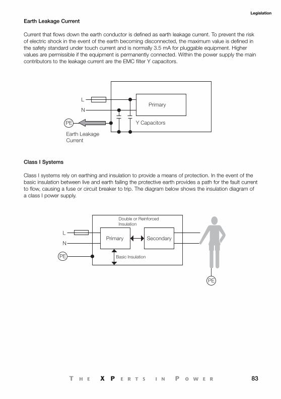
83
Legislation
Earth Leakage Current
Current that flows down the earth conductor is defined as earth leakage current. To prevent the riskof electric shock in the event of the earth becoming disconnected, the maximum value is defined inthe safety standard under touch current and is normally 3.5 mA for pluggable equipment. Highervalues are permissible if the equipment is permanently connected. Within the power supply the maincontributors to the leakage current are the EMC filter Y capacitors.
Class I Systems
Class I systems rely on earthing and insulation to provide a means of protection. In the event of thebasic insulation between live and earth failing the protective earth provides a path for the fault currentto flow, causing a fuse or circuit breaker to trip. The diagram below shows the insulation diagram ofa class I power supply.
Primary
Y Capacitors
L
N
PE
Earth Leakage Current
PE
Primary Secondary
Basic Insulation
L
N
PE
Double or Reinforced Insulation
Legislation_150210.qxp:Layout 1 21/6/10 09:49 Page 83
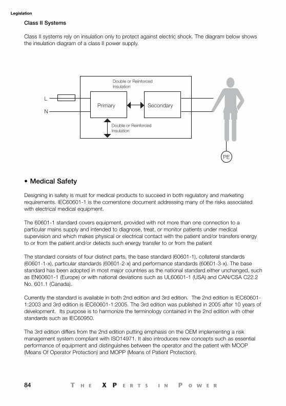
84
Legislation
Class II Systems
Class II systems rely on insulation only to protect against electric shock. The diagram below showsthe insulation diagram of a class II power supply.
Primary SecondaryL
N
Double or Reinforced Insulation
Double or Reinforced Insulation
PE
• Medical Safety
Designing in safety is must for medical products to succeed in both regulatory and marketingrequirements. IEC60601-1 is the cornerstone document addressing many of the risks associatedwith electrical medical equipment.
The 60601-1 standard covers equipment, provided with not more than one connection to aparticular mains supply and intended to diagnose, treat, or monitor patients under medicalsupervision and which makes physical or electrical contact with the patient and/or transfers energyto or from the patient and/or detects such energy transfer to or from the patient
The standard consists of four distinct parts, the base standard (60601-1), collateral standards(60601-1-x), particular standards (60601-2-x) and performance standards (60601-3-x). The basestandard has been adopted in most major countries as the national standard either unchanged, suchas EN60601-1 (Europe) or with national deviations such as UL60601-1 (USA) and CAN/CSA C22.2No. 601.1 (Canada).
Currently the standard is available in both 2nd edition and 3rd edition. The 2nd edition is IEC60601-1:2003 and 3rd edition is IEC60601-1:2005. The 3rd edition was published in 2005 after 10 years ofdevelopment. Its purpose is to harmonize the terminology contained in the 2nd edition with otherstandards such as IEC60950.
The 3rd edition differs from the 2nd edition putting emphasis on the OEM implementing a riskmanagement system compliant with ISO14971. It also introduces new concepts such as essentialperformance of equipment and distinguishes between the operator and the patient with MOOP(Means Of Operator Protection) and MOPP (Means of Patient Protection).
Legislation_150210.qxp:Layout 1 21/6/10 09:49 Page 84
85
Legislation
The concept of MOPP and MOOP allows the manufacturer relaxation in terms of creepage & clearancedistances for MOOP if it is proven through risk management that the equipment will not come intocontact with the patient in normal operation or under a single fault condition. The requirements forMOOP follow IEC60950 and for MOPP follow those required in IEC60601-1 2nd edition.
The structure of the base standard is hazard specific and provides requirements for evaluating thecommon hazards associated with electro-medical products. Its scope is to protect both patientsand operators by reducing the likelihood of electric shock, mechanical, radiation, ignition offlammable anaesthetics, fire and excessive output energy hazards.
The basic concept of the standard requires that two means of protection (MOP) or two levels ofprotection (LOP) under IEC60601-1 2nd edition are employed in various areas of the product so thatif one fails the product will retain another means of protection to contain any electrical shock hazardfrom either the patient or the operator.
To achieve these two means of protection, 60601-1 permits the use of three building blocks used indifferent combinations. These building blocks are insulation, protective earth and protectionimpedance. For example protective earth (1 x MOP) used in conjunction with basic insulation (1 xMOP) provides the two means of protection required. The table below lists the permitted buildingblocks and the means of protection they provide.
Before the design can start the insulation class of the equipment must be determined; whether theequipment will be class I (reliant on protective earth) or class II (not reliant on protective earth) asmust the classification of the applied part if applicable.
Building Block Means of Protection Provided
Protective Earth 1
Basic Insulation 1
Supplementary Insulation 1
Double Insulation 2
Reinforced Insulation 2
Applied parts are circuits that deliberately come into contact with the patient and are classified astype B, type BF or type CF each providing a degree of protection against electric shock.
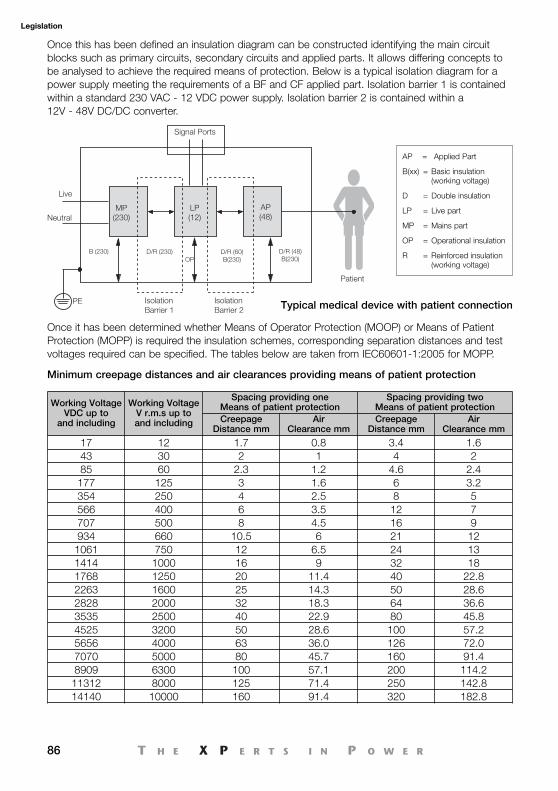
86
Legislation
Working VoltageVDC up to
and including
Working VoltageV r.m.s up to and including
Spacing providing oneMeans of patient protection
Spacing providing twoMeans of patient protection
Creepage Distance mm
Air Clearance mm
Creepage Distance mm
Air Clearance mm
17 12 1.7 0.8 3.4 1.643 30 2 1 4 285 60 2.3 1.2 4.6 2.4177 125 3 1.6 6 3.2354 250 4 2.5 8 5566 400 6 3.5 12 7707 500 8 4.5 16 9934 660 10.5 6 21 121061 750 12 6.5 24 131414 1000 16 9 32 181768 1250 20 11.4 40 22.82263 1600 25 14.3 50 28.62828 2000 32 18.3 64 36.63535 2500 40 22.9 80 45.84525 3200 50 28.6 100 57.25656 4000 63 36.0 126 72.07070 5000 80 45.7 160 91.48909 6300 100 57.1 200 114.211312 8000 125 71.4 250 142.814140 10000 160 91.4 320 182.8
Once this has been defined an insulation diagram can be constructed identifying the main circuitblocks such as primary circuits, secondary circuits and applied parts. It allows differing concepts tobe analysed to achieve the required means of protection. Below is a typical isolation diagram for apower supply meeting the requirements of a BF and CF applied part. Isolation barrier 1 is containedwithin a standard 230 VAC - 12 VDC power supply. Isolation barrier 2 is contained within a 12V - 48V DC/DC converter.
Live
Neutral
Isolation Barrier 1
Isolation Barrier 2
Signal Ports
MP(230)
LP(12)
AP(48)
D/R (230) D/R (60)B(230)
D/R (48)B(230)
Patient
PE
B (230)OP
Typical medical device with patient connection
Minimum creepage distances and air clearances providing means of patient protection
AP = Applied Part
B(xx) = Basic insulation(working voltage)
D = Double insulation
LP = Live part
MP = Mains part
OP = Operational insulation
R = Reinforced insulation(working voltage)
Once it has been determined whether Means of Operator Protection (MOOP) or Means of PatientProtection (MOPP) is required the insulation schemes, corresponding separation distances and testvoltages required can be specified. The tables below are taken from IEC60601-1:2005 for MOPP.
Legislation_150210.qxp:Layout 1 21/6/10 09:49 Page 86
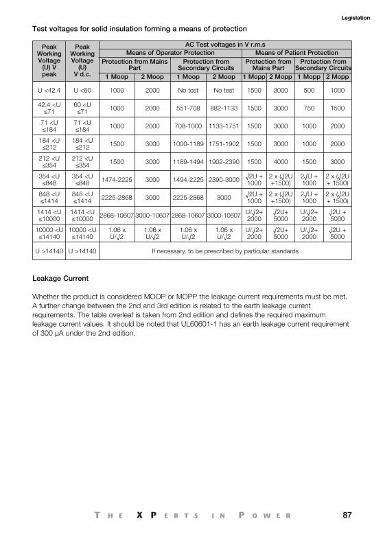
87
Legislation
Test voltages for solid insulation forming a means of protection
Peak WorkingVoltage
(U) V peak
Peak WorkingVoltage
(U) V d.c.
AC Test voltages in V r.m.sMeans of Operator Protection Means of Patient Protection
Protection from MainsPart
Protection fromSecondary Circuits
Protection fromMains Part
Protection fromSecondary Circuits
1 Moop 2 Moop 1 Moop 2 Moop 1 Mopp 2 Mopp 1 Mopp 2 Mopp
U <42.4 U <60 1000 2000 No test No test 1500 3000 500 1000
42.4 <U≤71
60 <U≤71 1000 2000 551-708 882-1133 1500 3000 750 1500
71 <U≤184
71 <U≤184 1000 2000 708-1000 1133-1751 1500 3000 1000 2000
184 <U≤212
184 <U≤212 1500 3000 1000-1189 1751-1902 1500 3000 1000 2000
212 <U≤354
212 <U≤354 1500 3000 1189-1494 1902-2390 1500 4000 1500 3000
354 <U≤848
354 <U≤848 1474-2225 3000 1494-2225 2390-3000 √2U +
10002 x (√2U+1500)
2√U +1000
2 x (√2U+ 1500)
848 <U≤1414
848 <U≤1414 2225-2868 3000 2225-2868 3000 √2U +
10002 x (√2U+1500)
2√U +1000
2 x (√2U+ 1500)
1414 <U≤10000
1414 <U≤10000 2868-10607 3000-10607 2868-10607 3000-10607 U/√2+
2000√2U+5000
U/√2+2000
√2U +5000
10000 <U≤14140
10000 <U≤14140
1.06 x U/√2
1.06 x U/√2
1.06 x U/√2
1.06 x U/√2
U/√2+2000
√2U+5000
U/√2+2000
√2U +5000
U >14140 U >14140 If necessary, to be prescribed by particular standards
Leakage Current
Whether the product is considered MOOP or MOPP the leakage current requirements must be met.A further change between the 2nd and 3rd edition is related to the earth leakage currentrequirements. The table overleaf is taken from 2nd edition and defines the required maximumleakage current values. It should be noted that UL60601-1 has an earth leakage current requirementof 300 μA under the 2nd edition.
Legislation_150210.qxp:Layout 1 21/6/10 09:49 Page 87

88
Legislation
N.C - Normal ConditionS.F.C - Single Fault Condition
(1) The only S.F.C for earth leakage current is the interruption of one supply conductor at a time.
(2) Equipment which has no protectively earthed accessible parts and no means for the protectiveearthing of other equipment and which complies with the requirements for the enclosure leakagecurrent and for the patient leakage current, if applicable.
(3) Equipment specified to be permanently installed with a protective earth conductor which iselectrically so connected that it can only be loosened with the aid of a tool and which is sofastened or otherwise so secured mechanically at a specific location that it can only be movedafter the use of a tool.
(4) Mobile X-ray equipment and mobile equipment with mineral insulation.
(5) The maximum values for the AC component of the patient leakage current and of the patientauxiliary current specified in the table refer to the AC-only component of the currents.
In the 3rd edition the earth leakage current requirement specified in notes (2) & (4) has been relaxed to5 mA in normal operation and 10 mA under a single fault condition. The requirements for touchcurrent (formally enclosure leakage current) remain at 100 μA in normal operation and 500 μA undera single fault condition.
For a power supply in a class I system the key parameter is the single fault earth leakage current. Anallowable single fault condition is to open the protective earth. In this instance earth leakage currentbecomes touch current.
Allowable values of continuous leakage and patient auxiliary currents, in milliamperes
CurrentType B Type BF Type CF
N.C. S.F.C N.C. S.F.C N.C. S.F.C
Earth Leakage Current General 0.5 1(1) 0.5 1(1) 0.5 1(1)
Earth Leakage Current for Equipmentaccording to notes (2) & (4) 2.5 5(1) 2.5 5(1) 2.5 5(1)
Earth Leakage Current for Equipmentaccording to note (3) 5 10(1) 5 10(1) 5 10(1)
Enclosure Leakage Current 0.1 0.5 0.1 0.5 0.1 0.5
Patient Leakage Current DCaccording to note (5) AC
0.010.1
0.050.5
0.010.1
0.050.5
0.010.01
0.050.05
Patient Leakage Current (Mains voltage onthe signal input part or signal output part) - 5 - - - -
Patient Leakage Current (Mains voltage onthe applied part) - - - 5 - 0.05
Patient Auxiliary Current DCaccording to note (5) AC
0.010.1
0.050.5
0.010.1
0.050.5
0.010.01
0.050.05
Legislation_150210.qxp:Layout 1 21/6/10 09:49 Page 88
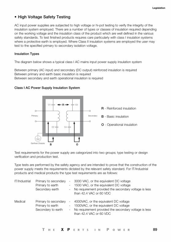
89
Legislation
• High Voltage Safety Testing
AC input power supplies are subjected to high voltage or hi-pot testing to verify the integrity of theinsulation system employed. There are a number of types or classes of insulation required dependingon the working voltage and the insulation class of the product which are well defined in the varioussafety standards. To test finished products requires care particularly with class I insulation systemswhere a protective earth is employed. Where Class II insulation systems are employed the user maytest to the specified primary to secondary isolation voltage.
Insulation Types
The diagram below shows a typical class I AC mains input power supply insulation system
Between primary (AC input) and secondary (DC output) reinforced insulation is requiredBetween primary and earth basic insulation is requiredBetween secondary and earth operational insulation is required
Primary
C1
C2 C4
C3R
B O
Secondary
Earthed Chassis
R - Reinforced insulation
B - Basic insulation
O - Operational insulation
Class I AC Power Supply Insulation System
Test requirements for the power supply are categorized into two groups; type testing or designverification and production test.
Type tests are performed by the safety agency and are intended to prove that the construction of thepower supply meets the requirements dictated by the relevant safety standard. For IT/Industrialproducts and medical products the type test requirements are as follows:
IT/Industrial Primary to secondary - 3000 VAC, or the equivalent DC voltagePrimary to earth - 1500 VAC, or the equivalent DC voltageSecondary earth - No requirement provided the secondary voltage is less
than 42.4 VAC or 60 VDC
Medical Primary to secondary - 4000VAC, or the equivalent DC voltagePrimary to earth - 1500VAC, or the equivalent DC voltageSecondary to earth - No requirement provided the secondary voltage is less
than 42.4 VAC or 60 VDC
Legislation_150210.qxp:Layout 1 21/6/10 09:49 Page 89
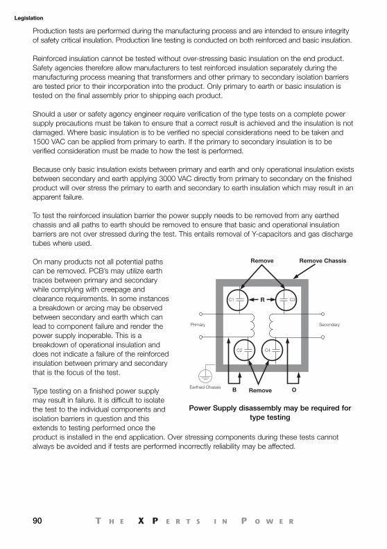
90
Legislation
Production tests are performed during the manufacturing process and are intended to ensure integrityof safety critical insulation. Production line testing is conducted on both reinforced and basic insulation.
Reinforced insulation cannot be tested without over-stressing basic insulation on the end product.Safety agencies therefore allow manufacturers to test reinforced insulation separately during themanufacturing process meaning that transformers and other primary to secondary isolation barriersare tested prior to their incorporation into the product. Only primary to earth or basic insulation istested on the final assembly prior to shipping each product.
Should a user or safety agency engineer require verification of the type tests on a complete powersupply precautions must be taken to ensure that a correct result is achieved and the insulation is notdamaged. Where basic insulation is to be verified no special considerations need to be taken and1500 VAC can be applied from primary to earth. If the primary to secondary insulation is to beverified consideration must be made to how the test is performed.
Because only basic insulation exists between primary and earth and only operational insulation existsbetween secondary and earth applying 3000 VAC directly from primary to secondary on the finishedproduct will over stress the primary to earth and secondary to earth insulation which may result in anapparent failure.
To test the reinforced insulation barrier the power supply needs to be removed from any earthedchassis and all paths to earth should be removed to ensure that basic and operational insulationbarriers are not over stressed during the test. This entails removal of Y-capacitors and gas dischargetubes where used.
On many products not all potential pathscan be removed. PCB’s may utilize earthtraces between primary and secondarywhile complying with creepage andclearance requirements. In some instancesa breakdown or arcing may be observedbetween secondary and earth which canlead to component failure and render thepower supply inoperable. This is abreakdown of operational insulation anddoes not indicate a failure of the reinforcedinsulation between primary and secondarythat is the focus of the test.
Type testing on a finished power supplymay result in failure. It is difficult to isolatethe test to the individual components andisolation barriers in question and thisextends to testing performed once theproduct is installed in the end application. Over stressing components during these tests cannotalways be avoided and if tests are performed incorrectly reliability may be affected.
Primary
Earthed Chassis
C1
C2 C4
C3R
Remove Remove Chassis
RemoveB O
Secondary
Power Supply disassembly may be required fortype testing
Legislation_150210.qxp:Layout 1 21/6/10 09:49 Page 90
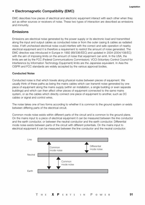
91
Legislation
• Electromagnetic Compatibility (EMC)
EMC describes how pieces of electrical and electronic equipment interact with each other when theyact as either sources or receivers of noise. These two types of interaction are described as emissionsand immunity.
Emissions
Emissions are electrical noise generated by the power supply or its electronic load and transmittedalong the input and output cables as conducted noise or from the outer casing & cables as radiatednoise. If left unchecked electrical noise could interfere with the correct and safe operation of nearbyelectrical equipment and it is therefore a requirement to restrict the amount of noise generated. TheEMC directive was introduced in Europe in 1992 (89/336/EEC) and updated in 2004 (2004/108/EC)with the aim of imposing limits on the amount of noise that equipment can emit. In the USA, thelimits are set by the FCC (Federal Communications Commission). VCCI (Voluntary Control Council forInterference by Information Technology Equipment) limits are the Japanese equivalent. In Asia theCISPR and FCC standards are widely accepted by the various approval bodies.
Conducted Noise
Conducted noise is that which travels along physical routes between pieces of equipment. Weusually think of these paths as being the mains cables which can transmit noise generated by onepiece of equipment along the mains supply (within an installation, a single building or even separatebuildings) and which can then affect other pieces of equipment connected to the same mainssystem, or as the cables which directly connect one piece of equipment to another, such as DCcables or signal and control wires.
The noise takes one of two forms according to whether it is common to the ground system or existsbetween differing parts of the electrical circuit.
Common mode noise exists within different parts of the circuit and is common to the ground plane.On the mains input to a piece of electrical equipment it can be measured between the line conductorand the earth conductor, or between the neutral conductor and the earth conductor. Differentialmode noise exists between parts of the circuit with different potentials. On the mains input toelectrical equipment it can be measured between the line conductor and the neutral conductor.
Differential mode noise
Common mode noise
Line
Neutral
Earth
Common mode noise
Legislation_150210.qxp:Layout 1 21/6/10 09:49 Page 91
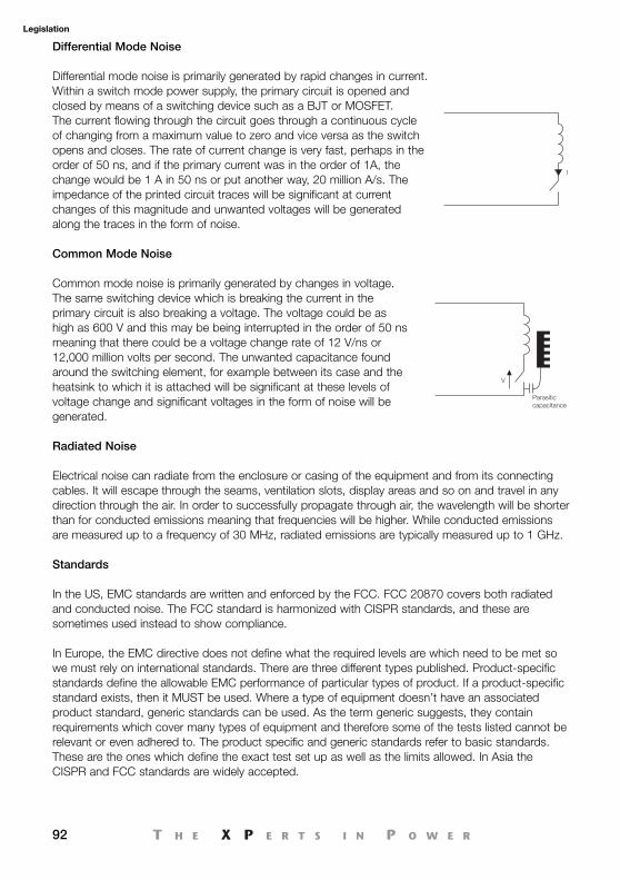
92
Legislation
Differential Mode Noise
Differential mode noise is primarily generated by rapid changes in current. Within a switch mode power supply, the primary circuit is opened and closed by means of a switching device such as a BJT or MOSFET. The current flowing through the circuit goes through a continuous cycle of changing from a maximum value to zero and vice versa as the switchopens and closes. The rate of current change is very fast, perhaps in theorder of 50 ns, and if the primary current was in the order of 1A, thechange would be 1 A in 50 ns or put another way, 20 million A/s. Theimpedance of the printed circuit traces will be significant at currentchanges of this magnitude and unwanted voltages will be generated along the traces in the form of noise.
Common Mode Noise
Common mode noise is primarily generated by changes in voltage.The same switching device which is breaking the current in theprimary circuit is also breaking a voltage. The voltage could be ashigh as 600 V and this may be being interrupted in the order of 50 nsmeaning that there could be a voltage change rate of 12 V/ns or12,000 million volts per second. The unwanted capacitance foundaround the switching element, for example between its case and theheatsink to which it is attached will be significant at these levels ofvoltage change and significant voltages in the form of noise will begenerated.
Radiated Noise
Electrical noise can radiate from the enclosure or casing of the equipment and from its connectingcables. It will escape through the seams, ventilation slots, display areas and so on and travel in anydirection through the air. In order to successfully propagate through air, the wavelength will be shorterthan for conducted emissions meaning that frequencies will be higher. While conducted emissionsare measured up to a frequency of 30 MHz, radiated emissions are typically measured up to 1 GHz.
Standards
In the US, EMC standards are written and enforced by the FCC. FCC 20870 covers both radiatedand conducted noise. The FCC standard is harmonized with CISPR standards, and these aresometimes used instead to show compliance.
In Europe, the EMC directive does not define what the required levels are which need to be met sowe must rely on international standards. There are three different types published. Product-specificstandards define the allowable EMC performance of particular types of product. If a product-specificstandard exists, then it MUST be used. Where a type of equipment doesn’t have an associatedproduct standard, generic standards can be used. As the term generic suggests, they containrequirements which cover many types of equipment and therefore some of the tests listed cannot berelevant or even adhered to. The product specific and generic standards refer to basic standards.These are the ones which define the exact test set up as well as the limits allowed. In Asia theCISPR and FCC standards are widely accepted.
I
V
Parasitic capacitance
Legislation_150210.qxp:Layout 1 21/6/10 09:49 Page 92
93
Legislation
For power supplies, the product-specific standard, IEC61204-3, takes precedence over the genericstandards. For emissions, it defines the following basic standards:
CISPR22 for conducted emissions (maximum of level B)CISPR22 for radiated emissions (maximum of level A)IEC61000-3-2 for harmonic currentsIEC61000-3-3 for voltage flicker
Sometimes there are other basic standards which need to be applied. For example, EN55014 isapplicable to motor operated household equipment, CISPR11 is applicable to industrial, scientific andmedical equipment. These basic standards will be called into use by product family standards whichmay be applicable to end user equipment.
Methods of Measurement
Noise measurement techniques are defined by the relevant basic standard. The techniques will begenerally similar whether it is an IT standard such as CISPR22 which is applicable or a militarystandard such as MIL 461 or DEF STAN 59-41.
Conducted Noise
Conducted noise values will largely be dependent upon the local impedance of the mains system atthe location at which the measurement is being done. Mains impedances will vary throughout anetwork and they could be vastly different throughout the world. A Line Impedance StabilizationNetwork (LISN), also known as an Artificial Mains Network (AMN) is used to give a defined mainsimpedance to the measurement system of 50 Ohms. In the case of the IT standard CISPR22, thenoise will be measured from 150 kHz to 30 MHz and two readings must be taken. These are a quasipeak measurement and an average measurement. Both must be under their respective limit lines inorder for the equipment to pass.
Radiated Noise
The services of a dedicated test house will normally be required to measure radiated noise. This isbecause the test should be performed on a large area known as an Open Area Test Site (OATS) whichwill not only be free of reflecting surfaces but will also be calibrated so that the influence of anyreflections from far away is known as the reflections will either add to the original signal, or detractfrom it depending upon the phase shift of the reflection. The measuring equipment will consist of anantenna which will feed into a receiver. The emissions from all sides of the equipment must be takenand for each face the antenna will be moved between heights of one and four meters to obtain theworst case reading. In addition to this, the antenna will be positioned with its elements alternatelyhorizontal and vertical, again to obtain the worst case reading.
As this setup is impractical for most companies, alternative techniques are normally used to give anindication of the radiated emissions. This may consist of using near field probes to ‘sniff’ around theenclosure of the equipment or using conducted emission techniques to measure at frequencies intothe hundreds of MHz band. This is a relevant test as it will often be the cables themselves that are thesource of the radiation.
Legislation_150210.qxp:Layout 1 21/6/10 09:49 Page 93
94
Legislation
EMC Filtering
A power supply or DC/DC converter will have an in-built input filter toreduce the conducted emissions. It will have two parts; one to reducethe common mode noise, the other to reduce the differential modenoise. Common mode noise can be reduced by use of Y capacitorsbetween line and ground and another one between neutral and groundin conjunction with a common mode inductor.
Differential mode noise can be reduced by use of an X capacitorbetween the line and the neutral in conjunction with a differential modeinductor. In some instances the differential mode inductor is formedfrom the leakage inductance of the common mode inductor so thatthere is only one visible wound component.
When combined the resulting filter may look like this:
Sometimes the built-in filter will give an inadequate performance for a given application. This may bewhere the power supply is designed to meet the lesser requirements of an industrial environment butis being used in the more stringent light industrial or residential environment. Perhaps several powersupplies are being used in a single piece of equipment and the resulting emissions must be reduced,or perhaps noise from the load itself is being coupled into the input of the power supply. In all theseinstances some form of external filtering will be required.
Filter Selection
There are some basic steps to follow when choosing a filter, some of which are straightforward andothers less so.
Mechanical format Is the filter going to be mounted within the equipment where it can befixed to a panel or should it also provide the extra functions of being themains input connector and perhaps contain an on/off switch? If it is theformer, a chassis mount filter can be used. These will generally havefaston terminals for easy connection but may also come with flyingleads. IEC inlet filters can have built-in on/off switches and even fuseholders. They can be mounted by either screwing them down to theequipment or by use of self locking lugs. Generally, for metal chassisequipment, the bolt-down variety will provide a lower impedance earthpath for the circulating noise down to ground.
L
N
Y
Y
L
N
X X
Y
Y
L
N
X X
Legislation_150210.qxp:Layout 1 21/6/10 09:49 Page 94
95
Legislation
Input current The filter should be able to pass the maximum working current of theequipment so as not to overheat but generally the lower the currentcapacity within a filter series, the higher its filtering performance.
Attenuation required A filter will be required to reduce the noise at certain frequencies. Byhow much and at which frequencies is information which will not readilybe known without having first performed a conducted noisemeasurement. Filters have differing amounts of attenuation and, for agiven current rating, the higher the attenuation the larger the filter. Asthere will be a practical limit on the size of filter components, largeamounts of attenuation will require the use of multi-stage filters.
Immunity
Immunity is concerned with how a piece of equipment will behave when subject to external electricalor magnetic influences in the form of noise. The noise will exist as either conducted or radiated noiseand will be from natural sources such as lightning, electrostatic build up or solar radiation or may befrom man made sources such as radio or mobile phone transmissions, commutation noise fromelectrical motors or emissions from power supplies and other switching devices.
Conducted Immunity Phenomena
A power supply or piece of electrical equipment will be subject to conducted noise either via themains connection, a DC output or via the signal and control lines. The noise could take various formsfrom brown-outs of the mains, to single short duration but high voltage spikes, to RF frequency noisecoupled into the cables and conducted into the equipment.
Radiated Immunity Phenomena
Noise can also directly enter a system via the air in the form of electrical or magnetic fields. The fieldis picked up by the cables attached to a piece of equipment or by the internal PCBs themselves andcan be in the form of electromagnetic fields generated by a mobile phone or the magnetic fieldgenerated from a nearby transformer.
Standards
The product standard for power supplies, EN61204-3, lists all of the basic immunity standards thatare applicable to a power supply. These are listed below. For each type of test there are twoimportant factors: the test severity level and the performance criteria which defines how theequipment operates while the test is being carried out.
Performance criteria A There is no change in operating status of the equipment. For a power supplythis means that it will continue to operate and no signals will change state.
Performance criteria B There is a loss of function while the test is being applied, but when the teststops, the operating parameters automatically return to normal. For a powersupply, this means that the output may go out of regulation and signals maychange state but only during the test.
Legislation_150210.qxp:Layout 1 21/6/10 09:49 Page 95
96
Legislation
Performance criteria C There is a loss of function while the test is being applied and a manual resetor intervention is required to restore the original operating parameters.
Electrostatic discharge: IEC61000-4-2
There are three types of test specified in the standard; contact discharge, air discharge anddischarge onto a coupling plane. The test is to simulate the effect of a person charging themselvesup (to many kV) and then touching either the equipment directly or adjacent equipment which couldin turn affect the equipment’s behavior. For open frame power supplies, this test is not normallyapplicable but for other power supplies, the pass conditions are ±4 kV for contact discharge and±8 kV for air discharge and coupling plane discharge, all with minimum performance criteria B.
RF electromagnetic field: IEC61000-4-3
This test simulates the fields given off by mobile phones and DECT phones. The field is generated bya sweeping signal generator with a 1 kHz modulation function. The signal is amplified and radiatedusing an antenna. The field strengths are high enough and in the frequency band (80 MHz to 1 GHz)to prevent local radio and TV stations and more importantly emergency services communicationsfrom working so the test must be performed in a screened chamber. For power supplies intended tooperate in a light industrial or residential environments, the field strength is 3 V/m but for industrialpower supplies the required field strength is 10 V/m. Minimum performance criteria is B in both cases.
Electrical fast transients: IEC61000-4-4
This test is to simulate switching transients generated by motor or solenoid activation or perhapsfrom fluorescent lighting. The pulse is very short, only 50ns with a 5ns rise time and is appliedbetween the two lines and the earth. Generally, the test is only applied to the AC input as the DClines and the signal and control lines on a power supply are normally too short. For power suppliesintended to operate in light industrial or residential environments the pulse is ±1 kV but for industrialpower supplies the required pulse is ±2 kV. Minimum performance criteria is B in both cases.
Voltage surge: IEC61000-4-5
This test is to simulate the effects of a near lightning strike. The duration and energy content of the pulseare much greater than for the electrical fast transients test with the duration being 50 μs with a 1.2 μsrise time. The pulse is applied between each line and earth and also between lines themselves. Forpower supplies the pulse is ±2 kV common mode, ±1 kV differential, with a minimum of performancecriteria B in both cases.
RF conducted: IEC61000-4-6
This test is similar to the RF radiated electromagnetic field test and must be applied under similarconditions within a screened chamber though the frequency range is 150 kHz to 80 MHz. For powersupplies intended to operate in a light industrial or residential environments, the coupled noise is3 Vrms but for industrial power supplies the coupled noise is 10 Vrms. Performance criteria B is theminimum applicable in both cases.
Legislation_150210.qxp:Layout 1 21/6/10 09:49 Page 96

97
Legislation
Voltage dips and interruptions: IEC61000-4-11
A voltage dip represents the brown-out conditions experienced from time to time on the power grid,while a voltage interruption represents a complete black out condition. There are 3 parts to the test;a 30% dip for 10 ms with minimum performance criteria B, a 60% dip for 100 ms with minimumperformance criteria C and a >95% interruption for 5 seconds with minimum performance criteria C.
• CE Marking
CE marking within Europe was established as a means of identifying a product as meeting all therelevant European directives. These directives have been introduced as a way of allowing free tradewithin the EU member states as individual members are no longer allowed to prevent trade ontechnical grounds. By displaying the CE mark, the product is identified to customs and bordercontrols as complying with the necessary directives. There are many directives which are applicablefor CE marking and these include:
- Low voltage equipment - Simple pressure vessels- Toys - Construction products- Electromagnetic compatibility - Machinery- Personal protection equipment - Non automatic weighing machines- Active implantable medical devices - Gas appliances- Hot water boilers - Civil explosives- Medical devices - Potentially explosive atmospheres- Recreational craft - Lifts- Refrigeration appliances - Pressure equipment- Telecommunications terminal equipment - In vitro diagnostic medical devices- Radio & telecommunications terminal equipment
For component power supplies only the Low Voltage Directive (LVD) is applicable. For external powersupplies the EMC directive and the Energy Related Products (ErP) directive also apply.
Low Voltage Directive (LVD) 2006/95/EC
The LVD is applicable to equipment designed for use with a voltage rating of between 50 and 1000VAC and between 75 and 1500 VDC. The directive itself does not define how to comply with it butby conforming to one of the relevant standards, such as the IT safety standard EN60950,compliance is demonstrated. The route to compliance is by generating a Technical Construction File(TCF) which includes the following:
- General description of the electrical equipment- Conceptual design and manufacturing drawings- Description and explanation of these designs and drawings- Listing of the product standards used as safety reference- Results of design calculations and examinations- Test reports
Legislation_150210.qxp:Layout 1 21/6/10 09:49 Page 97
98
Legislation
Electromagnetic Compatibility (EMC) Directive 2004/108/EC
This directive is applicable to apparatus liable to cause electromagnetic disturbance or the performanceof which is liable to be affected by such disturbance. Again, the directive does not state howcompliance should be achieved, but there are two routes to compliance. The first is the standards routewhereby the product is tested against either product specific or generic standards. The second is thetechnical construction file route. This would be chosen where a piece of equipment may be too large toundergo testing, or it may be that some of the tests are just not relevant. The arguments for this wouldbe laid down in the TCF which would be assessed and signed off by a competent body.
Energy Related Products Directive (ErP) 2009/125/EC
The ErP (formerly known as EuP) Directive provides a framework for setting eco-design requirementsfor energy related products. Commission regulation No 278/2009 implements the directive for externalpower supplies with regard to no load power consumption and active efficiency based on the quantitysold within the EU and the end application.
Declaration of Conformity (DofC)
The CE mark should be accompanied by a declaration of conformity. This will list:
- Name & address of the manufacturer- Description of the equipment- Reference to harmonized product standards used- Name of the signatory and their position- Last two digits of the year in which the CE marking was affixed
This is a self declaration that the manufacturer (or person who places the product on the market inthe EU) has taken all necessary steps to ensure compliance with all the relevant directives.
The Low Voltage Directive relates to open frame, component and external power supplies. The EMCDirective relates to external power supplies. The ErP Directive relates to external power supplies sold inhigh volumes within the EU for office equipment and consumer electronics applications.
The CE mark on an open frame or component power supply shows that it complies to the LVD, the CEmark on an external power supply shows that it complies with the LVD & EMC Directives and whereapplicable the ErP Directive.
• Defense and Avionics EMC Standards
For power supplies operated in these environments there are standards maintained by government orinternational organisations such as the US Department of Defense (MIL-STD), the UK Ministry ofDefense (DEF STAN), the French military (GAM-EG) & NATO (STANAG).
Many countries use the MIL-STD series of standards maintained by the US Department of Defense,but have national deviations covering specific conditions or equipment used by their armed forces.EMC standards are typically organised by service (air force, army, navy etc.), environment (above andbelow deck for example), test details, equipment and specification limits. There are standards coveringimmunity, conducted emissions and radiated emissions. The key elements for power supplies are theconducted immunity and conducted emissions standards which are discussed overleaf.
Legislation_150210.qxp:Layout 1 21/6/10 09:49 Page 98
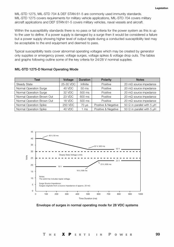
99
Legislation
Test Voltage Duration Polarity Notes
Steady State 25-30 VDC Infinite Positive 20 mΩ source impedanceNormal Operation Surge 40 VDC 50 ms Positive 20 mΩ source impedanceNormal Operation Surge 32 VDC 500 ms Positive 20 mΩ source impedanceNormal Operation Brown Out 23 VDC 600 ms Positive 20 mΩ source impedanceNormal Operation Brown Out 18 VDC 500 ms Positive 20 mΩ source impedanceNormal Operation Spike 250 VDC 70 μs Positive & Negative 50 Ω in parallel with 5 μHNormal Operation Spike 40 VDC 1 ms Positive & Negative 50 Ω in parallel with 5 μH
MIL-STD 1275, MIL-STD 704 & DEF STAN 61-5 are commonly used immunity standards.MIL-STD 1275 covers requirements for military vehicle applications, MIL-STD 704 covers militaryaircraft applications and DEF STAN 61-5 covers military vehicles, naval vessels and aircraft.
Within the susceptibility standards there is no pass or fail criteria for the power system as this is upto the user to define. If a power supply is damaged by a surge then it would be considered a failurebut a power supply showing higher level of output ripple during a conducted susceptibility test maybe acceptable to the end equipment and deemed to pass.
Typical susceptibility tests cover abnormal operating voltages which may be created by generatoronly supplies or emergency power, voltage surges, voltage spikes & voltage drop outs. The tablesand graphs following outline some of the key criteria for 24/28 V nominal supplies.
MIL-STD 1275-D Normal Operating Mode
Envelope of surges in normal operating mode for 28 VDC systems
45
40
25
30
35
20
15
10
5
0
0 100 200 300 400 500 600 700 800 900 1000
Volts
Time Duration (ms)
32 V
23 V
18 V
Steady State Voltage Limits
40 V, 50 ms
Notes:The solid line includes ripple voltage.
Surge Source Impedance:Surges originate from a source impedance of approx. 20 mΩ
23 V, 600 ms
32 V, 500 ms
18 V, 500 ms
Legislation_150210.qxp:Layout 1 21/6/10 09:49 Page 99
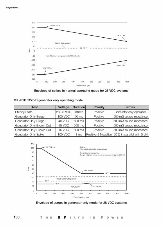
100
Legislation
Test Voltage Duration Polarity Notes
Steady State 23-33 VDC Infinite Positive Generator only operationGenerator Only Surge 100 VDC 50 ms Positive 500 mΩ source impedanceGenerator Only Surge 40 VDC 500 ms Positive 500 mΩ source impedanceGenerator Only Brown Out 15 VDC 500 ms Positive 500 mΩ source impedanceGenerator Only Brown Out 16 VDC 600 ms Positive 500 mΩ source impedanceGenerator Only Spike 100 VDC 1 ms Positive & Negative 50 Ω in parallel with 5 μH
MIL-STD 1275-D generator only operating mode
Envelope of surges in generator only mode for 28 VDC systems
Envelope of spikes in normal operating mode for 28 VDC systems
300
250
200
150
100
50
0
-50
-100
-150
-200
-250
-300
0 100 200 300 400 500 600 700 800 900 1000
250 V, 70 µs
100 V, 1 ms
-100 V, 1 ms
-250 V, 70 µs
25 - 30 V
Steady State Voltage
Note: Maximum energy content of 15 millijoules
Volts
Time Duration (µs)
80
90
100
110
70
40
50
60
30
20
10
0
0 100 200 300 400 500 600 700 800 900 1000
Volts
Time Duration (ms)
40 V
16 V15 V
33 V
23 VSteady State Voltage Limits
Notes:The solid line includes ripple voltage.
Surge Source Impedance:Surges originate from a source impedance of approx. 500 mΩ
100 V, 50 ms
40 V, 500 ms
15 V, 500 ms 16 V, 600 ms
Legislation_150210.qxp:Layout 1 21/6/10 09:49 Page 100
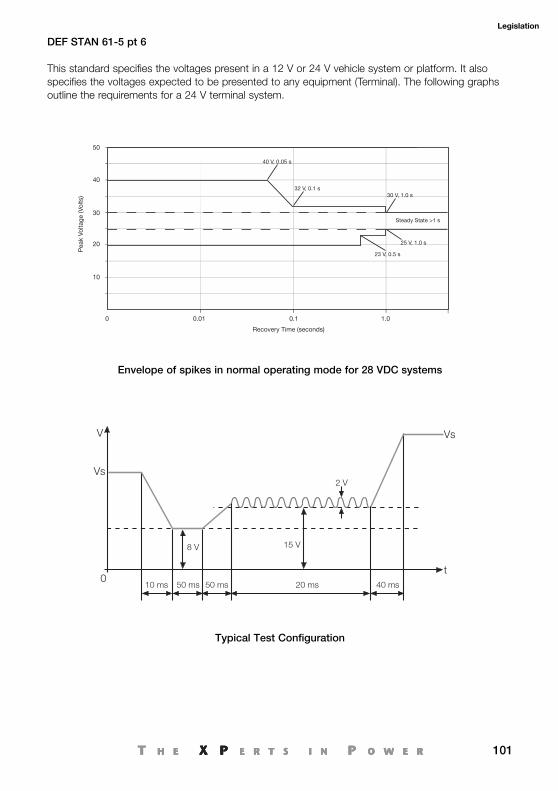
101
Legislation
DEF STAN 61-5 pt 6
This standard specifies the voltages present in a 12 V or 24 V vehicle system or platform. It alsospecifies the voltages expected to be presented to any equipment (Terminal). The following graphsoutline the requirements for a 24 V terminal system.
Envelope of spikes in normal operating mode for 28 VDC systems
Typical Test Configuration
50
40
30
20
10
0 0.01 0.1 1.0
Pea
k Vo
ltage
(Vol
ts)
Recovery Time (seconds)
40 V, 0.05 s
32 V, 0.1 s30 V, 1.0 s
Steady State >1 s
25 V, 1.0 s
23 V, 0.5 s
Vs
Vs
t
V
010 ms 50 ms 50 ms 20 ms 40 ms
2 V
15 V8 V
Legislation_150210.qxp:Layout 1 21/6/10 09:49 Page 101
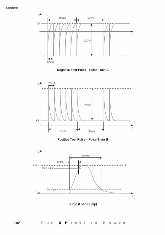
102
Legislation
Negative Test Pulse - Pulse Train A
Vs
t
V
-200 V
90 ms10 ms
100 µs
Positive Test Pulse - Pulse Train B
100 µs
Vs
t
V
90 ms10 ms
200 V
Surge (Load Dump)
Vst
V
174 V90% V pk
10% V pk
V pk
10 ms
350 ms
Legislation_150210.qxp:Layout 1 21/6/10 09:49 Page 102
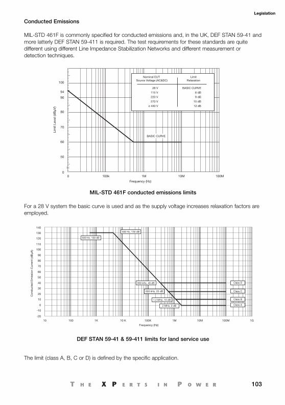
103
Legislation
Conducted Emissions
MIL-STD 461F is commonly specified for conducted emissions and, in the UK, DEF STAN 59-41 andmore latterly DEF STAN 59-411 is required. The test requirements for these standards are quitedifferent using different Line Impedance Stabilization Networks and different measurement ordetection techniques.
For a 28 V system the basic curve is used and as the supply voltage increases relaxation factors areemployed.
The limit (class A, B, C or D) is defined by the specific application.
MIL-STD 461F conducted emissions limits
DEF STAN 59-41 & 59-411 limits for land service use
100
90
94
Lim
it Le
vel (
dB
µV)
Frequency (Hz)
80
70
60
50
00 100k 1M 10M 100M
Nominal EUT Source Voltage (AC&DC)
28 V
115 V
220 V
270 V
≥ 440 V
BASIC CURVE
6 dB
9 dB
10 dB
12 dB
LimitRelaxation
BASIC CURVE
140
130
120
110
100
90
80
70
60
50
40
30
20
10
0
-10
-20
Con
duc
ted
Em
issi
on C
urre
nt (d
BµA
)
Frequency (Hz)
10 100 1K 10 K 100K 1M 10M 100M 1G
Class A
500 Hz, 130 dB
500 Hz, 130 dB
300 kHz, 40 dB
600 kHz, 25 dB
1.2 MHz, 10 dB
2 MHz, 0 dB
Class B
Class C
Class D
Legislation_150210.qxp:Layout 1 21/6/10 09:49 Page 103
104
Legislation
• No Load Power Consumption and Efficiency Legislation for ExternalPower Supplies
Two important reasons for controlling the power consumed by external power supplies are continuityof the energy supply and reduction of environmental impacts. Targets are given for external suppliesbecause high quantities are sold, they normally do not have an off button and they are commonly leftplugged into the mains supply when not in use.
Many areas of the world have introduced limits for no load power consumption and active efficiencyof external power supplies. In the US there are three main parties, these being; California EnergyCommission (CEC), US Congress with its Energy Independence and Security Act (EISA), both ofwhich are mandatory and finally Energy Star which is voluntary.
In Europe there is the Energy related Products (ErP) Directive formally known as the Energy usingProducts (EuP) Directive. Other parts of the world that are enacting legislation are mainly basing theirlimits on previous Energy Star requirements.
Both CEC and ErP have standardized their requirements with Energy Star to reduce the confusion ofmultiple limits. In the US, the CEC limits changed on 1st July 2008 and the Energy Star limitschanged on 1st Nov 2008. In Europe, the limits changed on 1st Jan, 2009.
The tables within Summary of Limits show the limits imposed by the four bodies. The averageefficiency is taken as the mean of individual efficiencies at 25%, 50%, 75% and 100% loads.
Energy Independence & Security Act 2007 (EISA)
In 2007 the US Congress passed a law effective 1st July, 2008, called the Energy Independence andSecurity Act of 2007 (EISA). This states that single output external power supplies of less than 250 Wmanufactured on or after 1st July 2008 should meet maximum no load power consumption, andminimum active load efficiency limits with an input of 115 VAC, 60 Hz.
These requirements are identical to the 1st July, 2008 CEC limits meaning that any power supplymeeting efficiency level IV will comply with the EISA requirements. There are four exceptions includedin the EISA legislation:-
The power supply is to be used in an application requiring Federal Food and Drug Administrationlisting and approval as a medical device.
The power supply is charging either a detachable battery pack or the internal battery pack of aproduct which is primarily motor operated.
The power supply is to be used for spares for a product that was manufactured before 1st July, 2008.
The power supply is to be subsequently exported outside of the US.
Legislation_150210.qxp:Layout 1 21/6/10 09:49 Page 104
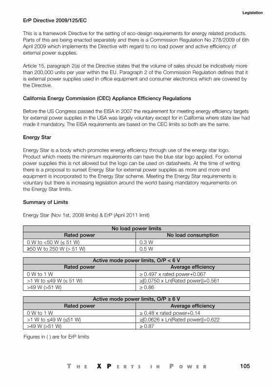
105
Legislation
ErP Directive 2009/125/EC
This is a framework Directive for the setting of eco-design requirements for energy related products.Parts of this are being enacted separately and there is a Commission Regulation No 278/2009 of 6thApril 2009 which implements the Directive with regard to no load power and active efficiency ofexternal power supplies.
Article 15, paragraph 2(a) of the Directive states that the volume of sales should be indicatively morethan 200,000 units per year within the EU. Paragraph 2 of the Commission Regulation defines that itis external power supplies used in office equipment and consumer electronics which are covered bythe Directive.
California Energy Commission (CEC) Appliance Efficiency Regulations
Before the US Congress passed the EISA in 2007 the requirement for meeting energy efficiency targetsfor external power supplies in the USA was largely voluntary except for in California where state law hadmade it mandatory. The EISA requirements are based on the CEC limits so both are the same.
Energy Star
Energy Star is a body which promotes energy efficiency through use of the energy star logo.Product which meets the minimum requirements can have the blue star logo applied. For externalpower supplies this is not allowed but the logo can be used on datasheets. At the time of writingthere is a proposal to sunset Energy Star for external power supplies as more and more endequipment is incorporated to the Energy Star scheme. Meeting the Energy Star requirements isvoluntary but there is increasing legislation around the world basing mandatory requirements on the Energy Star limits.
Summary of Limits
Energy Star (Nov 1st, 2008 limits) & ErP (April 2011 limit)
No load power limitsRated power No load consumption
0 W to <50 W (≤ 51 W) 0.3 W≥50 W to 250 W (> 51 W) 0.5 W
Active mode power limits, O/P < 6 VRated power Average efficiency
0 W to 1 W ≥ 0.497 x rated power+0.067>1 W to ≤49 W (≤ 51 W) ≥[0.0750 x Ln(Rated power)]+0.561>49 W (>51 W) ≥ 0.86
Active mode power limits, O/P ≥ 6 VRated power Average efficiency
0 W to 1 W ≥ 0.48 x rated power+0.14>1 W to ≤49 W (≤51 W) ≥[0.0626 x Ln(Rated power)]+0.622>49 W (>51 W) ≥ 0.87
Figures in ( ) are for ErP limits
Legislation_150210.qxp:Layout 1 21/6/10 09:49 Page 105
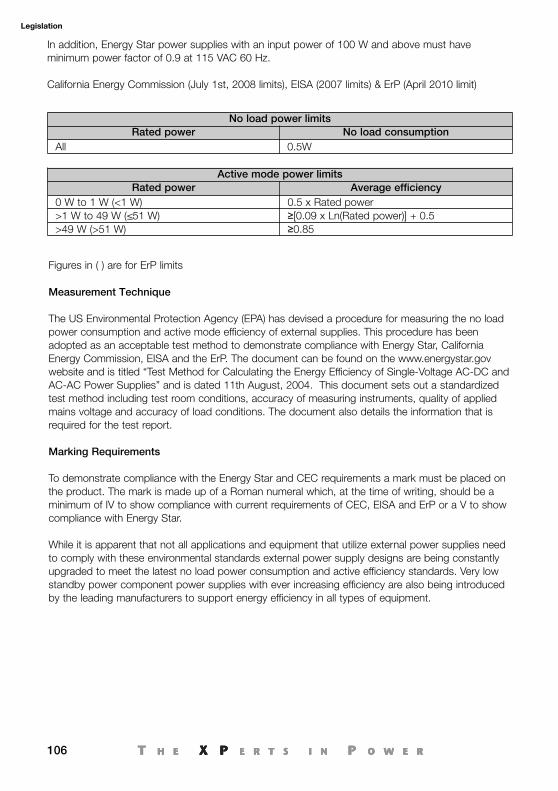
106
Legislation
Measurement Technique
The US Environmental Protection Agency (EPA) has devised a procedure for measuring the no loadpower consumption and active mode efficiency of external supplies. This procedure has beenadopted as an acceptable test method to demonstrate compliance with Energy Star, CaliforniaEnergy Commission, EISA and the ErP. The document can be found on the www.energystar.govwebsite and is titled “Test Method for Calculating the Energy Efficiency of Single-Voltage AC-DC andAC-AC Power Supplies” and is dated 11th August, 2004. This document sets out a standardizedtest method including test room conditions, accuracy of measuring instruments, quality of appliedmains voltage and accuracy of load conditions. The document also details the information that isrequired for the test report.
Marking Requirements
To demonstrate compliance with the Energy Star and CEC requirements a mark must be placed onthe product. The mark is made up of a Roman numeral which, at the time of writing, should be aminimum of IV to show compliance with current requirements of CEC, EISA and ErP or a V to showcompliance with Energy Star.
While it is apparent that not all applications and equipment that utilize external power supplies needto comply with these environmental standards external power supply designs are being constantlyupgraded to meet the latest no load power consumption and active efficiency standards. Very lowstandby power component power supplies with ever increasing efficiency are also being introducedby the leading manufacturers to support energy efficiency in all types of equipment.
In addition, Energy Star power supplies with an input power of 100 W and above must haveminimum power factor of 0.9 at 115 VAC 60 Hz.
California Energy Commission (July 1st, 2008 limits), EISA (2007 limits) & ErP (April 2010 limit)
No load power limitsRated power No load consumption
All 0.5W
Active mode power limitsRated power Average efficiency
0 W to 1 W (<1 W) 0.5 x Rated power>1 W to 49 W (≤51 W) ≥[0.09 x Ln(Rated power)] + 0.5>49 W (>51 W) ≥0.85
Figures in ( ) are for ErP limits
Legislation_150210.qxp:Layout 1 21/6/10 09:49 Page 106
107
Legislation
• Energy Efficiency of Component Power Supplies
It is easy to define active efficiency and no load power requirements of external power supplies butharder to define for component power supplies. External power supplies are considered a productin their own right with specific legislation but component power supplies are not.
Energy efficiency of component supplies relates to the end application when it falls within one of theproduct groups that Energy Star list (see next page). A product group may contain several products,for example the product group ‘imaging equipment’ covers digital duplicators, mailing machines,printers, scanners and all in ones.
In the case of a simple printer, the energy efficiency requirements depend on the printing technologyand the format size. The same power supply used in different types of printer will have differingenergy efficiency effects. In imaging equipment for example, there are two ways of demonstratingEnergy Star compliance. One is to use the Typical Electricity Consumption (TEC) method; the otheris to use the Operational Mode (OM) method.
The TEC approach reflects assumptions about how many hours a day the product is in general use,the pattern of use during those hours and the default delay times that the product has beforeentering a low power or sleep mode. Electricity consumption is measured in the form of accumulatedenergy used and converted to power by dividing by the test period.
The calculation takes into account that there will be two periods of use per day with a low powermode in between simulating a lunch break and it also assumes that there will be no weekend usage.
The TEC value is derived from the various energy measurements taken during active usage, sleepmode and auto off periods. The maximum allowable TEC value is dependant upon the format size,product speed (images per minute) and marking technology.
The OM approach is to measure power during the ready, standby and sleep modes and also tomeasure the default time period until the product enters sleep mode. To be compliant with EnergyStar, the product must to meet 3 criteria:-
• The default time to entering sleep mode must be less than a given value in minutes, depending onthe product format and speed (images per minute) for imaging equipment except for mailingmachines. For mailing machines the default sleep time delay is only dependant on speed (mailprocessed per minute).
• The standby power consumption must be less than 1 W for small and standard format productswithout fax capability or less than 2 W for small and standard format products with fax capability.For large format product and mailing machines there is currently no limit.
• The sleep power must be less than a given value according to type of machine, format size andprinting technology. There is a base figure for each case and this can be increased by the type offunctions that the product has beyond the basic print engine
From this it can be seen that factors other than the power supply contribute greatly to the energyefficiency rating of an imaging equipment application.
Legislation_150210.qxp:Layout 1 21/6/10 09:49 Page 107
108
Legislation
Energy Star Products
• Appliances
- Clothes washers
- Dehumidifiers
- Dishwashers
- Freezers
- Refrigerators
- Room Air Cleaners & Purifiers
- Water Coolers
- Vending Machines
• Commercial Food ServiceEquipment
- Commercial Dishwashers
- Commercial Fryers
- Commercial Griddles
- Commercial Hot Food HoldingCabinets
- Commercial Ice Machines
- Commercial Kitchen Package
- Commercial Ovens
- Commercial Refrigerators &Freezers
- Commercial Steam Cookers
• Computers & Electronics
- Audio / Video
- Battery Chargers
- Combination Units, TV/DVD & VCR/DVD
- Computers
- Cordless Phones
- Digital to Analog Converters
- Displays
- DVD & Blu Ray Products
- Enterprise Servers
- External Power Adapters
- Imaging Equipment
- Set-top Boxes & Cable Boxes
- Televisions
• Heating & Cooling
- Air Conditioning, Central
- Air Conditioning, Room
- Boilers
- Dehumidifiers
- Fans, Ventilating
- Furnaces
- Heat Pumps, Air Source
• Heating & Cooling...cont.
- Heat Pumps, Geothermal
- Home Sealing - Insulation &Air Sealing
- Light Commercial Heating &Cooling
- Room Air Cleaners & Purifiers
• Lighting and Fans
- Commercial LED Lighting
- Decorative Light Strings
- Fans, Ceiling
- Light Bulbs (CFLs)
- Light Fixtures
- Residential LED Lighting
• Plumbing
- Water Heater, Gas Condensing
- Water Heater, Heat Pump
- Water Heater, High EfficiencyGas Storage
- Water Heater, Solar
- Water Heater, Whole HomeGas Tankless
As each product type needs to meet differing requirements to comply with Energy Star it is notpossible to produce component power supplies which guarantee that equipment will be Energy Starcompliant.
The functions that the end application runs in standby or sleep mode, the time taken to enterstandby mode and the average energy consumed within a working day must all be taken intoaccount.
The latest component power supply designs minimize no load power consumption and maximizeactive efficiency by utilizing green mode control ICs and so provide OEM’s with the best possiblestarting point enabling the design and manufacture of Energy Star compliant product.
Legislation_150210.qxp:Layout 1 21/6/10 09:49 Page 108
109
Technology Editorial 1
• 95% High efficiency power supply changes the way high reliabilitysystems are designed
The size or power density of a power supply is a key criteria when selecting the optimum product fora given application. In applications where fans are not desirable due to noise or reliability concernsthen efficiency becomes of primary concern. Power supply technology has evolved to a point whereefficiencies in the 90-95% range are available. To put this into context a typical power supply in the1980’s would have been in the region of 75% efficient.
A designer by considering efficiency as an important criteria, can make fundamental design decisionsthat effect the overall system design in a positive way by:
1) Eliminating or reducing the need for system fan cooling
2) Reducing the overall size and weight of the system
3) Reducing the internal temperatures of the system and improving reliability
4) Enhancing system reliability
5) Reducing overall energy usage and the end user operating costs
Size and weight are prime considerations in the selection of power supplies. You can always find asmaller power supply, or design one, by including a fan to provide forced air-cooling. You might saveone-third to one half of the total volume of a typical unit in this way. One disadvantage of thisapproach is fan noise which is often restricted in applications such as audio systems, IT applications,medical devices and military systems. Other problems include a significant reduction in reliability asthe fan is likely be the only moving part in the power supply and adds a maintenance problem. In ahigh reliability design the fan will need to be monitored creating a need for additional circuitry. Due tothese issues, many system designers are now looking to utilize convection or conduction cooledpower supplies to power their equipment. Minimizing component-count will help in reducing size andcost, but this has limitations.
Equipment must be reliable in a variety of environments meaning that compromises with respect toimmunity to interference (EMC/EMI/RFI) and production of conducted or radiated emissions cannotbe tolerated.
Finally, we need to take account of green legislation including RoHS, no load or standby powerconsumption and efficiency, particularly if equipment is going to be sold around the world. The useof RoHS components is obligatory and designing for the highest possible efficiency will not only helpin meeting present and future environmental legislation but will also help to ensure best performancefrom convection-cooled power supplies. Breakthrough technologies that have a dramatic impact onpower supply design are rare. Advances in power semiconductor technology have had the mostimpact, followed by improvements in magnetic materials and capacitors. Reducing power supplysize without compromising performance means that you have to work towards incrementalimprovements in every aspect of the design, both electrical and mechanical.
Editorials_170210.qxp:Layout 1 21/6/10 09:52 Page 109
110
Technology Editorial 1
The size - power - efficiency trade off
The surface area available to provide cooling is the limiting factor in how much heat you candissipate from a convection-cooled power supply – one that doesn’t need a fan. It follows that themore efficient you make the power supply, the less heat you’ll need to remove and the smaller theunit can be. What may appear to be small differences can have great impact here. If you can buy ordesign a power supply that is 95% efficient, versus one that’s 90% efficient, the 5% difference inefficiency means you need to remove less than half of the heat of the less efficient design. For a 250 Watt power supply, this means 14.6 W less heat to be dissipated. In systems designed forglobal use a power supply with a high efficiency across an 85 – 264 VAC input range is desirable.Efficiency will also be affected by load – most power supplies operate at maximum efficiency at 80-90% of rated load. It pays to check out the efficiency you can expect in your individual application.For example, most IT equipment averages at 30 – 40% of its maximum load in typical operation andthe efficiency of the power system will vary accordingly.
The frequency - size - efficiency trade off
One way to reduce the size of magnetic components and capacitors is to increase the switchingfrequency of the converter. However, switching losses increase with frequency. The trade-off forefficiency and switching frequency in a typical 200 W power supply produced during the last fewyears is shown in Figure 1.
90.0
92.0
94.0
88.0
86.0
84.0
82.030 40 50 60 70 80 90 100 110 120 130 140 150 160 170 180 190 200
Effi
cien
cy (%
)
Switching Frequency
Effect on efficiency of reducing component size (vis switching frequency)
Typical 200 W design
Figure 1: Effect on efficiency of reducing component size by increasing switching frequency
Clearly, there is a compromise between size, efficiency, switching frequency, reliability, lifetime,cooling technique and cost for a given power rating.
Editorials_170210.qxp:Layout 1 21/6/10 09:52 Page 110
111
Technology Editorial 1
Designing for 90%+ efficiency
The best of today’s 250 W, convection-cooled power supplies operate at over 90% efficiency acrossan input voltage range of 90 to 264 VAC. This level of efficiency is essential in order to keep withinan industry-standard 6 x 4 inch footprint while ensuring adequate heat dissipation without a coolingfan or large external heatsinks. Over 90% efficiency can only be achieved with near losslessswitching in the active power factor correction circuit, the main converter(s) and the rectifiers. A diagram for a 250 Watt AC/DC power supply that achieves up to 95% efficiency at 240 VAC inputand 92% efficiency at 90 VAC input is shown in Figure 2.
Figure 2: This 250 W AC/DC power supply is up to 95% efficient
From the outset achieving high efficiency was the primary design goal for this power supply.Consequently, for each stage the power loss budget was determined and this drove the choice ofcircuit topology. Power losses were minimized in each stage, striving to save every mW ofunnecessary dissipation. For example the input filter for the power supply shown above uses verylow resistance winding wire that virtually eliminates I2R losses in the chokes.
A quasi-resonant, lossless switching, power factor correction circuit operates in discontinuous mode.Its operating frequency varies between 30 kHz and 500 kHz to achieve Zero Current Switching (ZCS)throughout the specified range of loads and input voltages.
The ZCS power factor correction scheme is important because it ensures that the voltage switcheswhen the current is truly at zero, thereby eliminating switching losses. The main converters are afixed frequency resonant half-bridge design, phase shifted by 90˚, again with lossless ZCS. Twotransformers are employed; the combination has lower losses than if one larger transformer hadbeen utilized.
Editorials_170210.qxp:Layout 1 21/6/10 09:52 Page 111
112
Technology Editorial 1
Figure 3: Combining the outputs of two converters that are 90-degrees out of phase reducesripple level and doubles ripple frequency
Figure 4: ZCS and the use of resonant converters delivers high efficiency over a wide range ofloads and input voltages, not just at full load
A feedback loop monitors the power supply output and varies the boost converter voltage, which inturn varies the voltage at the input to the main converters. The primary purpose of the boostconverter is to boost the PFC voltage of approximately 380 to 420 VDC. This enables the design ofthe main converters to be optimized around tightly defined voltage parameters, another factor thathelps to achieve high efficiency. The final stage uses synchronous rectification instead ofconventional diodes as this greatly reduces power loss. Timing for the boost converter, mainconverters and synchronous rectifiers is precisely controlled to achieve accurate ZCS. A crystal-controlled clock is used as the timing reference and a divider network is employed to get to thedesired switching frequency. Using this approach is crucial for the efficient operation of synchronousrectifiers, especially for higher output voltages. This power supply architecture results in highefficiency across a wide range of loads and input voltages, as Figure 4 demonstrates.
Editorials_170210.qxp:Layout 1 21/6/10 09:52 Page 112
113
Technology Editorial 1
A further benefit of ZCS is the low level of both conducted and radiated emissions as well as theoutput ripple and noise. The power supply referred to in this paper exhibits less than 90mV peak-to-peak ripple and noise at 20 MHz bandwidth and is below the level B limit line for EN55022 forconducted and radiated emissions. When tested against the stringent MIL-STD 461F CE102 forconducted emissions this type of power supply passed with considerable margin opening the door ina range of high reliability applications without excessive EMI filtering and screening being needed.
Creative mechanical design
The thermal performance of a power supply can be greatly improved through creative mechanicaldesign. Avoiding hot spots and ensuring the best possible air-flow around components are bothimportant. XP Power’s CCM250 (Figure 5), has input chokes stacked above other components tosave board space. Normally this might create hotspots but the low-loss design of the chokesprevents them.
Figure 5: XP Power’s CCM250 power supply uses creative mechanical design to pack a 250 W (300 W peak) convection-cooled power supply into a 6 x 4 x 1.5 inch format
Editorials_170210.qxp:Layout 1 21/6/10 09:52 Page 113
114
Technology Editorial 1
All heat-generating components, including the power factor correction choke, are bonded directly tothe U-channel chassis, which doubles as an effective heatsink. Control circuits are placed ondaughter cards mounted at 90 degrees to the main printed circuit board. In other words, full use ismade of all the available space by thinking about the mechanical aspects of the unit in 3D at theoutset of the design.
Applications for this high efficiency technnology
• Sealed Military Systems
The combination of high efficiency and the heat sinking of components to the U channel enabled adesigner to use this type of power supply in a completely sealed enclosure for a military batterycharger that needed to be waterproof and dust proof. The high efficiency PSU helps eliminate thefan and improve reliability. The other benefit of the CCM250 is the excellent EMI performance thatenabled the customer to meet MIL-STD 461F CE, CS, RE & RS for Army Ground Applications.
• Green IT Systems
While most equipment designers don’t operate the equipment they design – energy costs are stillvery much of concern for the end users especially in applications that operate 24/7.
Consider this example – using a high efficiency PSU compared to a less efficient power supply thatuses cheaper components and less efficient technology may mean an improvement of 15%efficiency with only a small increase in the cost of the PSU. At typical energy costs of 12 cents perkWHour, and an average load of 200 W the end user will use substantially less energy per year andachieve cost savings of more than $40 per year. The high efficiency technology just paid for itself inless than one year!
Conclusion
Combining the best of proven design technologies with creative mechanical design has led recentlyto the introduction of units that can reach up to 95% efficiency, a figure thought impossible only afew years ago. Further incremental improvements will be harder to achieve, but the decades ofexperience that many engineers now have in power supply design, coupled with advances insemiconductor technology, will make them possible. By considering efficiency alongside cost and size when you select a power supply you can improve overall system cost, performance and reliability.
Editorials_170210.qxp:Layout 1 21/6/10 09:52 Page 114
115
Technology Editorial 2
• Putting the data into power supply datasheets
Contents
• Input Characteristics- Input Voltage Range- Earth Leakage Current- Inrush Current
• Output Characteristics- Overload Protection- Remote Sense- Output Accuracy and Minimum Loads- Output Ripple and Noise
• Efficiency• Reliability, Temperature and Cooling• EMC
Why is it that seemingly similar power supplies have significantly different performance and reliabilitycharacteristics? The answer may lie in the specification detail that can be missing from some datasheets, available only in the long-form data/application notes or may even be due to “specmanship”.
For this exercise we’ll look at typical data for an AC/DC power supply though many of the issuesmay equally apply to DC/DC converters.
Input Characteristics - Input voltage range
AC/DC power supplies are typically universal, meaning that they operate over a wide range of inputvoltages, normally from 85 or 90 VAC up to 264 VAC. This feature allows a single product to operateworld-wide without changes in configuration of the input stage. Some products utilize automaticinput voltage range selection giving two operating ranges; typically 90 to 132 VAC & 180 to 264 VAC. Universal input power supplies provide better immunity to supply disturbances in somecircumstances and this may be a benefit.
If the power supply is to be used close to its full power capability within the application it is importantto check the specification details on the available output power in the low input voltage area wheresome products de-rate by as much as 20 or 30%. This means that they may be operating outside ofspecification when operating from nominal 100 VAC or 115/120 VAC supplies or at the very leastmay infringe the design margins of the end equipment. Ignoring this de-rating in the available output power will seriously affect the reliability and life time of the power supply and therefore theend equipment.
De-rating the power supply output power at low input voltages is common in lower cost universalinput power supplies and is normally due to the limitations of the active power correction boost converters
Editorials_170210.qxp:Layout 1 21/6/10 09:52 Page 115
116
Technology Editorial 2
Earth leakage current
Earth leakage current is a parameter which varies widely from product to product. The earth leakagecurrent is largely a consequence of EMC filtering within the power supply and is normally only a keyconsideration in medical applications, equipment using multiple AC/DC products or where externalEMC filters are utilized to reduce overall system noise.
Inrush Current
A key consideration affecting the selection of fuses, filters and switchgear is the inrush current at thepoint of application of the AC power. The maximum inrush current is usually specified in the datasheet however there is more to this than a simple maximum value.
In lower power, lower cost products the inrush limiting is typically via a simple NTC thermistor whichwill provide protection from a “cold start” but may take a minute or more to return to its initial valueafter switch off. This results in an inrush current many times the specified maximum during an off/oncycle even with a relatively long delay. The inrush current is also likely be specified at 25 ºC and maybe significantly higher even for a cold start in higher ambient temperatures. In products above a fewhundred watts, this thermistor is likely to be taken out of circuit once the output voltage isestablished, to remove unnecessary power dissipation, removing this as an issue.
Inrush current is an important factor to be considered to avoid nuisance tripping of fuses and circuitbreakers as well as reliability of switches and filtering. The fuse rating given in some data sheets isusually the rating of the internal fuse which is designed to operate only in the event of catastrophicfailure and is not user replaceable. Determining the value of the equipment fuse needs to take intoaccount the normal maximum running current, the inrush current and the effects of aging. Theequipment fuse should also only be required to operate under catastrophic failure conditions as theelectronic power supply overload protection will cater for any problems on the DC side.
Output characteristics - Overload protection
All power supplies offer overload protection to protect both the power supply and the load trackingand wiring from overheating. This may come in a number of different guises or characteristics.
In low power products a trip and restart or “hiccup” mode is common as this helps to keep costsdown by utilizing primary control schemes. Trip & restart overload schemes are generally unsuitablefor loads involving high start up currents such as electromechanical equipment, lighting equipment orapplications which have a high capacitive element, as start up may be unreliable and variable evenfrom unit to unit. This overload characteristic is also unsuitable for direct battery chargingapplications. With these types of load a constant current overload characteristic is desirable.
Editorials_170210.qxp:Layout 1 21/6/10 09:52 Page 116
117
Technology Editorial 2
Remote Sense
Low voltage high current applications will benefit from products which offer remote sense where theoutput voltage can be measured at the point of load. This feature is particularly desirable where theload is variable. If the load is relatively constant then a simple user adjustment of the output voltagewill be adequate and more readily available though may result in other voltage rails also beingadjusted by the same percentage in multiple output supplies where the additional rails are oftensemi-regulated.
Output accuracy and minimum loads
Output accuracy or regulation is specified in many different ways by various manufacturers. It shouldencompass line regulation, load regulation, cross regulation (for multiple output supplies), transientresponse, initial set accuracy and temperature coefficient. These parameters can be specified overdiffering input ranges, load ranges, load step changes and temperature ranges etc. While theseitems can be presented in many ways the majority of single output supplies will have comparableperformance. Perhaps the most important consideration is for multiple output units where theperformance can be very different.
Single output power supplies rarely require a minimum load but multiple output units often requireminimum loads on one or more outputs and this should be made clear on the product data. Minimumloads are normally specified to reduce the effects of cross regulation between outputs and to maintainthe output accuracy within the specified limits. These minimum loads will need to be considered in thesystem design and where necessary components added to ensure that they are met.
As standby/no load power consumption requirements are introduced, the addition of minimum loadsbecomes a real system performance issue and other solutions are required. This is particularly true inlow power applications where features such as inhibit are rare due to market cost requirements andthe primary control systems in general use.
Output ripple & noise
Ripple & noise is one of the product performance specifications which is most open to interpretation,making comparison from the data sheet difficult if not impossible. The main variables are themeasurement bandwidth and the use of various external components and measurement techniques.The only real way to compare performance is to measure the products under the samemeasurement regime.
Efficiency
Most data sheets will offer a figure for efficiency allowing the user to quantify the waste heatgenerated within the end equipment. The efficiency of a power supply will vary dependant on theload and input voltage applied, so it is important to understand the unit’s efficiency under theoperating conditions of the application. Efficiency during operation at low line is typically lower than athigh line and may vary by as much as 6-7%. The most important parameter is the worst caseefficiency in order to understand the maximum waste heat generated by the supply.
Editorials_170210.qxp:Layout 1 21/6/10 09:52 Page 117
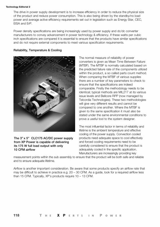
118
Technology Editorial 2
The drive in power supply development is to increase efficiency in order to reduce the physical sizeof the product and reduce power consumption. This is also being driven by the standby/no loadpower and average active efficiency requirements set out in legislation such as Energy Star, CEC,EISA and ErP.
Power density specifications are being increasingly used by power supply and dc/dc convertermanufacturers to convey advancement in power technology & efficiency. If these watts per cubicinch specifications are compared it is essential to ensure that the products have similar specificationsand do not require external components to meet various specification requirements.
Reliability, Temperature & Cooling
The normal measure of reliability of powerconverters is given as Mean Time Between Failure(MTBF). The MTBF is normally calculated based onthe predicted failure rate of the components utilizedwithin the product, a so called parts count method.When comparing the MTBF of various suppliesthere are a number of key parameters to check toensure that the specifications are indeedcomparable. Firstly the methodology needs to beidentical; typical methods are MIL217 at its variousissue levels and Bellcore RPP (now managed byTelcordia Technologies). These two methodologieswill give very different results and cannot becompared to one another. Where the MTBF isgiven to the same specification it must also bestated under the same environmental conditions toprove a useful tool to the system designer.
The most influential factor in terms of reliability andlifetime is the ambient temperature and effectivecooling of the power supply. Convection cooledproducts need adequate space to cool effectivelyand forced cooling requirements need to becarefully considered to ensure that the product isadequately cooled in the specific application.Manufacturers are increasingly providing key
measurement points within the sub assembly to ensure that the product will be both safe and reliableand to ensure adequate lifetime.
Airflow is another important consideration. Be aware that some products specify an airflow rate thatmay be difficult to achieve in practice e.g. 20 – 30 CFM. As a guide, look for a required airflow lessthan 15 CFM. Typically, XP’s products require 10 – 13 CFM.
The 3” x 5” CLC175 AC/DC power supplyfrom XP Power is capable of delivering its 175 W full load output with only 10 CFM airflow
Editorials_170210.qxp:Layout 1 21/6/10 09:52 Page 118
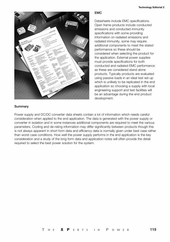
119
Technology Editorial 2
EMC
Datasheets include EMC specifications.Open frame products include conductedemissions and conducted immunityspecifications with some providinginformation on radiated emissions andradiated immunity, some may requireadditional components to meet the statedperformance so these should beconsidered when selecting the product forthe application. External power suppliesmust provide specifications for bothconducted and radiated EMC performanceas these are considered stand aloneproducts. Typically products are evaluatedusing passive loads in an ideal test set-upwhich is unlikely to be replicated in the endapplication so choosing a supply with localengineering support and test facilities willbe an advantage during the end productdevelopment.
Summary
Power supply and DC/DC converter data sheets contain a lot of information which needs carefulconsideration when applied to the end application. The data is generated with the power supply orconverter in isolation and in some instances additional components are required to meet the variousparameters. Cooling and de-rating information may differ significantly between products though thisis not always apparent in short form data and efficiency data is normally given under best case ratherthan worst case conditions. How well the power supply performs in the end application is the keyconsideration and a study of the long form data and application notes will often provide the detailrequired to select the best power solution for the system.
Editorials_170210.qxp:Layout 1 21/6/10 09:52 Page 119
120
Technology Editorial 3
• Medical power supplies: trends, challenges and design approaches
Contents
• Techniques for managing the design trade-offs• How small can they get?
Medical electronic equipment is getting smaller. Of course, this could be said of all electronic equipmentbut it is in the medical area that pressure for size and weight reduction is greatest. Not only is thehospital bedside environment very space-constrained but there is a trend for more equipment to be usedin the home, in doctors’ offices, and even in cars and on planes. This is creating particular pressure onpower supply manufacturers to reduce the size of their products.
In the last 10 years a typical convection-cooled, 100W AC/DC power supply has shrunk from a 4 x 7 inchfootprint in 1998 to just 2 x 4 inches today, a reduction of over 70%. This size reduction has had to bemanaged carefully. Smaller packages mean less area for heat dissipation, which in turn requires higherefficiency. This article explains some of the main design issues and briefly introduces some of the mosteffective techniques that are now employed to achieve power system design goals in medical applications.
Through both empirical measurement and calculation, estimates of the maximum power loss that achassis mount or open frame power supply can dissipate as heat for a given footprint are shown in Figure1. The figures are based on using convection cooling and on maintaining compliance with safety agencyrequirements. They also take account of providing reasonable operating life and acceptable reliability limits.Forced air cooling can improve the power rating considerably, but at the expense of decreased systemreliability, fans are fundamentally less reliable than the other power system components and they add tosystem size and noise. Fan noise is very undesirable in medical applications.
40.0
50.0
60.0
30.0
20.0
10.0
0.03
3 x 1.5 x0.84
4 x 2 x 1.24.5
4.5 x 2.5 x 1.25
5 x 3 x 1.35.5
5.5 x 3.7 x 1.366
6 x 4 x 1.6
Size (l x w x h) inches
MaximumPower Loss (W) Maximum Heat Loss versus Unit Size
Force cooledConvection cooled
Figure 1: The maximum safe heat dissipation vs. size for power supplies used in medical applications
Editorials_170210.qxp:Layout 1 21/6/10 09:52 Page 120
121
Technology Editorial 3
Figure 2 then shows how power loss translates into required efficiency.
For example, taking an industry standard footprint of 3 x 5 inches, convection cooling can effectivelyremove about 18 W of waste heat. Extrapolating from the 20 W power loss curve in Figure 2, a 120 W power supply needs to be at least 86% efficient for convection cooling to be sufficient.
Output Power versus Minimum Efficiency
70050W
45W
40W
35W
30W
25W
20W
15W
10W
5W
600
500
400
300
200
100
0
Output Power (W) Accepted Power Loss
Efficiency (%)
75 76 77 78 79 80 81 82 83 84 85 86 87 88 89 90 91 92 93 94 95
Figure 2: The minimum efficiency required for a given power supply output to ensurecompliance with safety standards
Figure 2 also shows the dramatic effect that a relatively small improvement in efficiency can have onthe available power from a power supply for a given heat dissipation. Taking the 20 W power losscurve, an efficiency gain from 88% to 93% would enable an power supply to deliver over 250 Wrather than around 150 W, within a given footprint.
For the power supply designer, size and efficiency are usually the most important trade-offs.Increasing the switching frequency means that smaller components can be used – notablycapacitors and inductors. However, switching losses rise and a power supply that may be 92%efficient at 30 kHz will be only 83% efficient at 200 kHz. Reliability is always of paramountimportance in medical applications, so keeping the power system running well within its maximumratings is always desirable. Finally, cost is the ever-present final determinant of a power supply’ssuitability for a given application.
Editorials_170210.qxp:Layout 1 21/6/10 09:52 Page 121
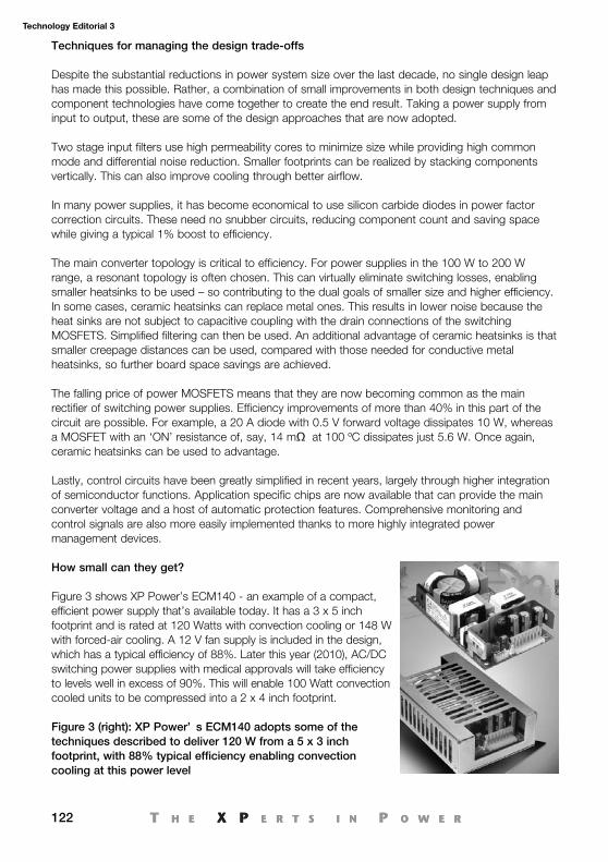
122
Technology Editorial 3
Techniques for managing the design trade-offs
Despite the substantial reductions in power system size over the last decade, no single design leaphas made this possible. Rather, a combination of small improvements in both design techniques andcomponent technologies have come together to create the end result. Taking a power supply frominput to output, these are some of the design approaches that are now adopted.
Two stage input filters use high permeability cores to minimize size while providing high commonmode and differential noise reduction. Smaller footprints can be realized by stacking componentsvertically. This can also improve cooling through better airflow.
In many power supplies, it has become economical to use silicon carbide diodes in power factorcorrection circuits. These need no snubber circuits, reducing component count and saving spacewhile giving a typical 1% boost to efficiency.
The main converter topology is critical to efficiency. For power supplies in the 100 W to 200 Wrange, a resonant topology is often chosen. This can virtually eliminate switching losses, enablingsmaller heatsinks to be used – so contributing to the dual goals of smaller size and higher efficiency.In some cases, ceramic heatsinks can replace metal ones. This results in lower noise because theheat sinks are not subject to capacitive coupling with the drain connections of the switchingMOSFETS. Simplified filtering can then be used. An additional advantage of ceramic heatsinks is thatsmaller creepage distances can be used, compared with those needed for conductive metalheatsinks, so further board space savings are achieved.
The falling price of power MOSFETS means that they are now becoming common as the mainrectifier of switching power supplies. Efficiency improvements of more than 40% in this part of thecircuit are possible. For example, a 20 A diode with 0.5 V forward voltage dissipates 10 W, whereasa MOSFET with an ‘ON’ resistance of, say, 14 mΩ at 100 ºC dissipates just 5.6 W. Once again,ceramic heatsinks can be used to advantage.
Lastly, control circuits have been greatly simplified in recent years, largely through higher integrationof semiconductor functions. Application specific chips are now available that can provide the mainconverter voltage and a host of automatic protection features. Comprehensive monitoring andcontrol signals are also more easily implemented thanks to more highly integrated powermanagement devices.
How small can they get?
Figure 3 shows XP Power’s ECM140 - an example of a compact,efficient power supply that’s available today. It has a 3 x 5 inchfootprint and is rated at 120 Watts with convection cooling or 148 Wwith forced-air cooling. A 12 V fan supply is included in the design,which has a typical efficiency of 88%. Later this year (2010), AC/DCswitching power supplies with medical approvals will take efficiencyto levels well in excess of 90%. This will enable 100 Watt convectioncooled units to be compressed into a 2 x 4 inch footprint.
Figure 3 (right): XP Power’ s ECM140 adopts some of thetechniques described to deliver 120 W from a 5 x 3 inchfootprint, with 88% typical efficiency enabling convectioncooling at this power level
Editorials_170210.qxp:Layout 1 21/6/10 09:52 Page 122
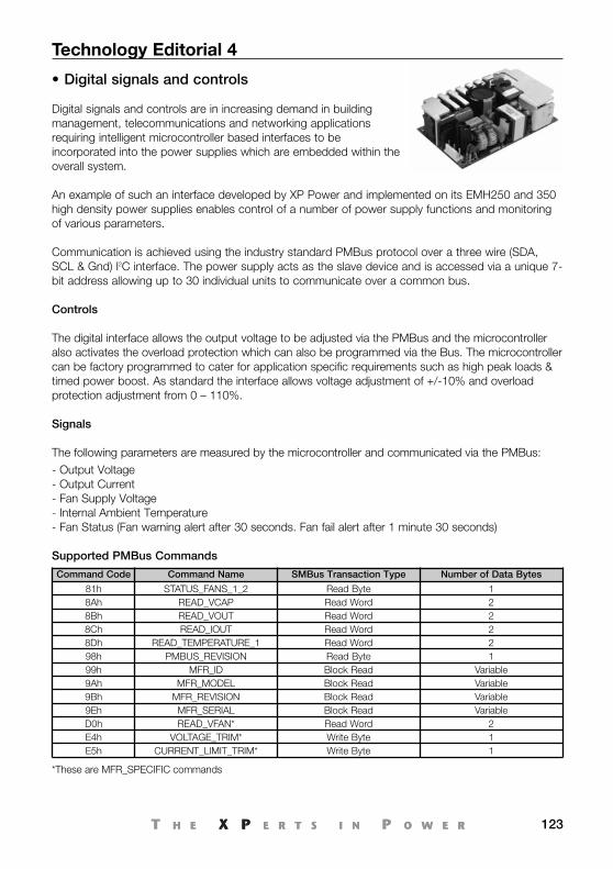
123
Technology Editorial 4
• Digital signals and controls
Digital signals and controls are in increasing demand in buildingmanagement, telecommunications and networking applicationsrequiring intelligent microcontroller based interfaces to beincorporated into the power supplies which are embedded within theoverall system.
An example of such an interface developed by XP Power and implemented on its EMH250 and 350high density power supplies enables control of a number of power supply functions and monitoringof various parameters.
Communication is achieved using the industry standard PMBus protocol over a three wire (SDA,SCL & Gnd) I2C interface. The power supply acts as the slave device and is accessed via a unique 7-bit address allowing up to 30 individual units to communicate over a common bus.
Controls
The digital interface allows the output voltage to be adjusted via the PMBus and the microcontrolleralso activates the overload protection which can also be programmed via the Bus. The microcontrollercan be factory programmed to cater for application specific requirements such as high peak loads &timed power boost. As standard the interface allows voltage adjustment of +/-10% and overloadprotection adjustment from 0 – 110%.
Signals
The following parameters are measured by the microcontroller and communicated via the PMBus:- Output Voltage- Output Current- Fan Supply Voltage- Internal Ambient Temperature- Fan Status (Fan warning alert after 30 seconds. Fan fail alert after 1 minute 30 seconds)
Supported PMBus Commands
Command Code Command Name SMBus Transaction Type Number of Data Bytes
81h STATUS_FANS_1_2 Read Byte 18Ah READ_VCAP Read Word 28Bh READ_VOUT Read Word 28Ch READ_IOUT Read Word 28Dh READ_TEMPERATURE_1 Read Word 298h PMBUS_REVISION Read Byte 199h MFR_ID Block Read Variable9Ah MFR_MODEL Block Read Variable9Bh MFR_REVISION Block Read Variable9Eh MFR_SERIAL Block Read VariableD0h READ_VFAN* Read Word 2E4h VOLTAGE_TRIM* Write Byte 1E5h CURRENT_LIMIT_TRIM* Write Byte 1
*These are MFR_SPECIFIC commands
Editorials_170210.qxp:Layout 1 21/6/10 09:52 Page 123
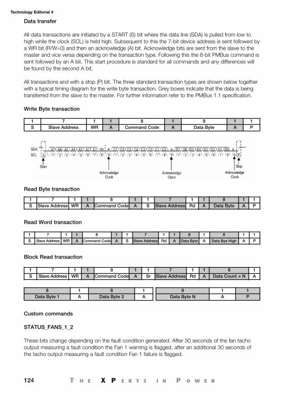
124
Technology Editorial 4
Data transfer
All data transactions are initiated by a START (S) bit where the data line (SDA) is pulled from low tohigh while the clock (SCL) is held high. Subsequent to this the 7-bit device address is sent followed bya WR bit (R/W=0) and then an acknowledge (A) bit. Acknowledge bits are sent from the slave to themaster and vice versa depending on the transaction type. Following this the 8-bit PMBus command issent followed by an A bit. This start procedure is standard for all commands and any differences willbe found by the second A bit.
All transactions end with a stop (P) bit. The three standard transaction types are shown below togetherwith a typical timing diagram for the write byte transaction. Grey boxes indicate that the data is beingtransferred from the slave to the master. For further information refer to the PMBus 1.1 specification.
Write Byte transaction
1 7 1 1 8 1 8 1 1S Slave Address WR A Command Code A Data Byte A P
1 7 1 1 8 1 1 7 1 1 8 1 1S Slave Address WR A Command Code A S Slave Address Rd A Data Byte A P
1 7 1 1 8 1 1 7 1 1 8 1 8 1 1
S Slave Address WR A Command Code A S Slave Address Rd A Data Byte A Data Bye High A P
1 7 1 1 8 1 1 7 1 1 8 1S Slave Address WR A Command Code A Sr Slave Address Rd A Data Count = N A
8 1 8 1Data Byte 1 A Data Byte 2 A
8 1 1Data Byte N A P
Read Byte transaction
Read Word transaction
Block Read transaction
Custom commands
STATUS_FANS_1_2
These bits change depending on the fault condition generated. After 30 seconds of the fan tachooutput measuring a fault condition the Fan 1 warning is flagged, after an additional 30 seconds ofthe tacho output measuring a fault condition Fan 1 failure is flagged.
Editorials_170210.qxp:Layout 1 21/6/10 09:52 Page 124
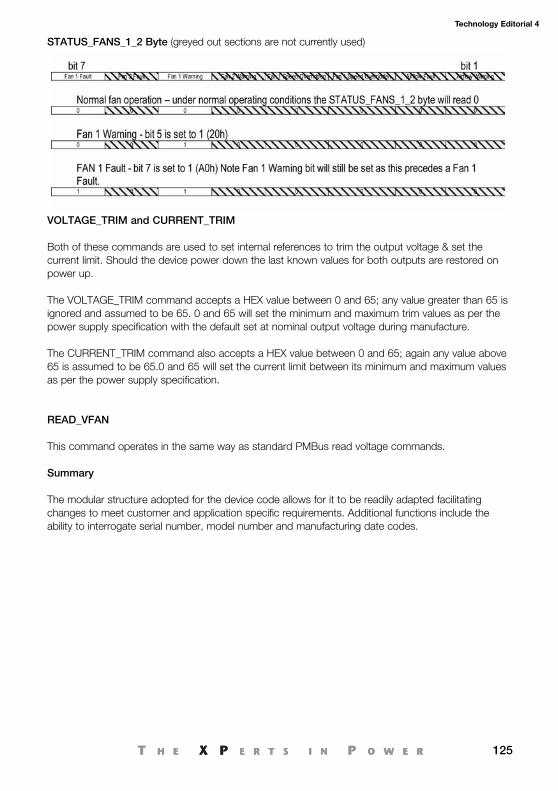
125
Technology Editorial 4
STATUS_FANS_1_2 Byte (greyed out sections are not currently used)
VOLTAGE_TRIM and CURRENT_TRIM
Both of these commands are used to set internal references to trim the output voltage & set thecurrent limit. Should the device power down the last known values for both outputs are restored onpower up.
The VOLTAGE_TRIM command accepts a HEX value between 0 and 65; any value greater than 65 isignored and assumed to be 65. 0 and 65 will set the minimum and maximum trim values as per thepower supply specification with the default set at nominal output voltage during manufacture.
The CURRENT_TRIM command also accepts a HEX value between 0 and 65; again any value above65 is assumed to be 65.0 and 65 will set the current limit between its minimum and maximum valuesas per the power supply specification.
READ_VFAN
This command operates in the same way as standard PMBus read voltage commands.
Summary
The modular structure adopted for the device code allows for it to be readily adapted facilitatingchanges to meet customer and application specific requirements. Additional functions include theability to interrogate serial number, model number and manufacturing date codes.
Editorials_170210.qxp:Layout 1 21/6/10 09:52 Page 125
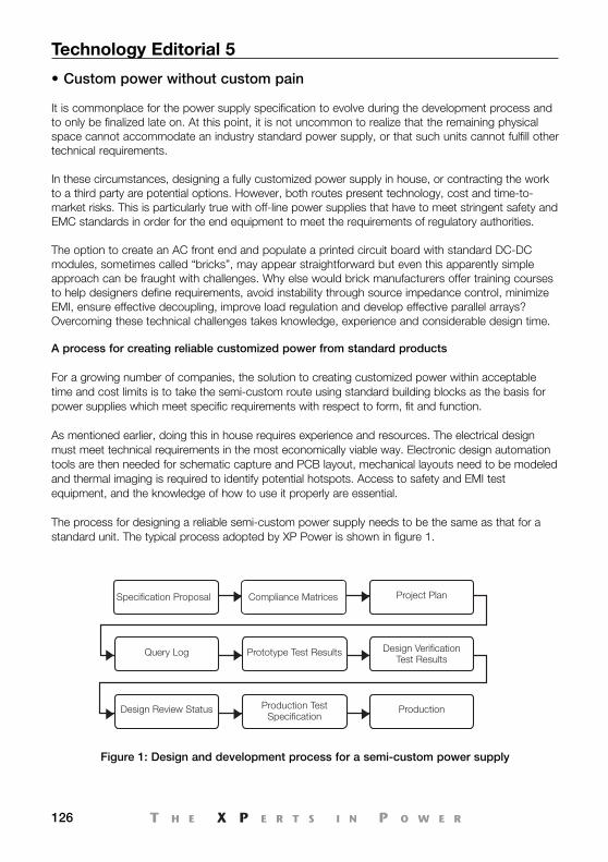
126
Technology Editorial 5
• Custom power without custom pain
It is commonplace for the power supply specification to evolve during the development process andto only be finalized late on. At this point, it is not uncommon to realize that the remaining physicalspace cannot accommodate an industry standard power supply, or that such units cannot fulfill othertechnical requirements.
In these circumstances, designing a fully customized power supply in house, or contracting the workto a third party are potential options. However, both routes present technology, cost and time-to-market risks. This is particularly true with off-line power supplies that have to meet stringent safety andEMC standards in order for the end equipment to meet the requirements of regulatory authorities.
The option to create an AC front end and populate a printed circuit board with standard DC-DCmodules, sometimes called “bricks”, may appear straightforward but even this apparently simpleapproach can be fraught with challenges. Why else would brick manufacturers offer training coursesto help designers define requirements, avoid instability through source impedance control, minimizeEMI, ensure effective decoupling, improve load regulation and develop effective parallel arrays?Overcoming these technical challenges takes knowledge, experience and considerable design time.
A process for creating reliable customized power from standard products
For a growing number of companies, the solution to creating customized power within acceptabletime and cost limits is to take the semi-custom route using standard building blocks as the basis forpower supplies which meet specific requirements with respect to form, fit and function.
As mentioned earlier, doing this in house requires experience and resources. The electrical designmust meet technical requirements in the most economically viable way. Electronic design automationtools are then needed for schematic capture and PCB layout, mechanical layouts need to be modeledand thermal imaging is required to identify potential hotspots. Access to safety and EMI testequipment, and the knowledge of how to use it properly are essential.
The process for designing a reliable semi-custom power supply needs to be the same as that for astandard unit. The typical process adopted by XP Power is shown in figure 1.
Specification Proposal Compliance Matrices Project Plan
Prototype Test Results Design VerificationTest Results
Query Log
Production TestSpecification
ProductionDesign Review Status
Figure 1: Design and development process for a semi-custom power supply
Editorials_170210.qxp:Layout 1 21/6/10 09:52 Page 126
127
Technology Editorial 5
After receiving a definition of requirements, the company draws up a specification proposal andcompliance matrix for the customer. These are reviewed and approved before a detailed project planis prepared. Development is often an iterative process, so a detailed “Query Log” is maintained toprovide a record of decisions taken along the way. Prototype testing is followed by provision of fulldesign verification test results. These include results of temperature cycling and other acceleratedaging tests, where appropriate. A detailed design review process is fully documented throughout thedevelopment of the product and a production test specification is agreed before it goes into fullproduction. The end result is a customized product that has been created to the same rigorousstandards as a standard power supply.
Typical customization options
Customization can be as simple as changing connectors. Other simple modifications includecustomizing covers with different fixings or producing custom wiring looms to reduce assembly timefor the end equipment.
Some of the most common requirements for more comprehensive customization are:
1. Additional input surge protection. This may be needed where the power supply is going to operatein a particularly demanding situation involving high-energy surges and voltage spikes. Thecustomization may involve creating a surge suppression circuit on a printed circuit board uponwhich a standard AC-DC power supply is then mounted.
2. Power factor correction. Some companies prefer to manage the DC-DC parts of power systemdesign in-house but do not have the expertise or resources to handle power factor correction(PFC). Standard PFC units may not be suitable, so a customized active or passive PFC modulemay be developed to fit the form and function needed.
3. Creating a Eurocard form factor. Eurocards are widely used in embedded systems but the rangeof Eurocard power supplies is limited. Designing a Eurocard to take a non-Eurocard format powersupply is a common requirement to give the system designer greater flexibility in the choice ofpower supply.
4. Eliminating fans. In some applications, fan cooling is not a viable option. As the only moving electro-mechanical part within a power supply, a fan will always represent a weak point with respect toreliability. Furthermore, the need to clean air filters adds a maintenance task. Where equipmentoperates in remote environments and maintenance becomes expensive, or where particularly harshoperating conditions limit product life, it’s often possible to design a standard power supply into aconvection-cooled package than can be bolted directly to the equipment enclosure.
5. Integration of batteries and charging circuits. Some applications require integral battery back-up toprotect against failure of the main input supply. Here, the power supply will include a chargingcircuit for the battery and automatic switching circuits, effectively turning a standard power supplyinto an uninterruptible power supply (UPS).
6. Addition of control and monitoring circuits. Customized control and monitoring can be added tomany power supplies and some vendors, including XP Power, have in-house expertise in writingsoftware for these functions. The addition of input and output “OK” signals, temperature sensorsand fan speed controllers are popular options.
Editorials_170210.qxp:Layout 1 21/6/10 09:52 Page 127
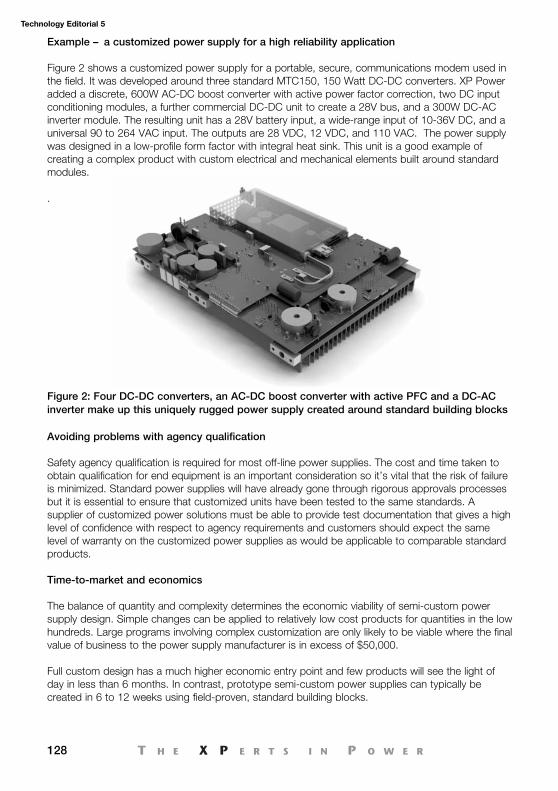
128
Technology Editorial 5
Example – a customized power supply for a high reliability application
Figure 2 shows a customized power supply for a portable, secure, communications modem used inthe field. It was developed around three standard MTC150, 150 Watt DC-DC converters. XP Poweradded a discrete, 600W AC-DC boost converter with active power factor correction, two DC inputconditioning modules, a further commercial DC-DC unit to create a 28V bus, and a 300W DC-ACinverter module. The resulting unit has a 28V battery input, a wide-range input of 10-36V DC, and auniversal 90 to 264 VAC input. The outputs are 28 VDC, 12 VDC, and 110 VAC. The power supplywas designed in a low-profile form factor with integral heat sink. This unit is a good example ofcreating a complex product with custom electrical and mechanical elements built around standardmodules.
.
Avoiding problems with agency qualification
Safety agency qualification is required for most off-line power supplies. The cost and time taken toobtain qualification for end equipment is an important consideration so it’s vital that the risk of failureis minimized. Standard power supplies will have already gone through rigorous approvals processesbut it is essential to ensure that customized units have been tested to the same standards. Asupplier of customized power solutions must be able to provide test documentation that gives a highlevel of confidence with respect to agency requirements and customers should expect the samelevel of warranty on the customized power supplies as would be applicable to comparable standardproducts.
Time-to-market and economics
The balance of quantity and complexity determines the economic viability of semi-custom powersupply design. Simple changes can be applied to relatively low cost products for quantities in the lowhundreds. Large programs involving complex customization are only likely to be viable where the finalvalue of business to the power supply manufacturer is in excess of $50,000.
Full custom design has a much higher economic entry point and few products will see the light ofday in less than 6 months. In contrast, prototype semi-custom power supplies can typically becreated in 6 to 12 weeks using field-proven, standard building blocks.
Figure 2: Four DC-DC converters, an AC-DC boost converter with active PFC and a DC-ACinverter make up this uniquely rugged power supply created around standard building blocks
Editorials_170210.qxp:Layout 1 21/6/10 09:52 Page 128
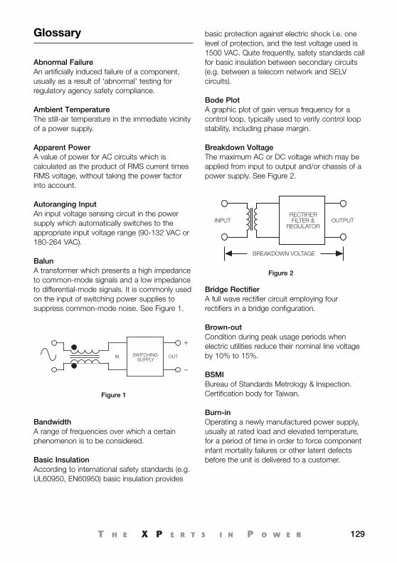
129
Glossary
Abnormal Failure An artificially induced failure of a component,usually as a result of ‘abnormal’ testing forregulatory agency safety compliance.
Ambient TemperatureThe still-air temperature in the immediate vicinityof a power supply.
Apparent PowerA value of power for AC circuits which iscalculated as the product of RMS current timesRMS voltage, without taking the power factorinto account.
Autoranging InputAn input voltage sensing circuit in the powersupply which automatically switches to theappropriate input voltage range (90-132 VAC or180-264 VAC).
BalunA transformer which presents a high impedanceto common-mode signals and a low impedanceto differential-mode signals. It is commonly usedon the input of switching power supplies tosuppress common-mode noise. See Figure 1.
BandwidthA range of frequencies over which a certainphenomenon is to be considered.
Basic InsulationAccording to international safety standards (e.g.UL60950, EN60950) basic insulation provides
basic protection against electric shock i.e. onelevel of protection, and the test voltage used is1500 VAC. Quite frequently, safety standards callfor basic insulation between secondary circuits(e.g. between a telecom network and SELVcircuits).
Bode PlotA graphic plot of gain versus frequency for acontrol loop, typically used to verify control loopstability, including phase margin.
Breakdown VoltageThe maximum AC or DC voltage which may beapplied from input to output and/or chassis of apower supply. See Figure 2.
Bridge RectifierA full wave rectifier circuit employing fourrectifiers in a bridge configuration.
Brown-outCondition during peak usage periods whenelectric utilities reduce their nominal line voltageby 10% to 15%.
BSMIBureau of Standards Metrology & Inspection.Certification body for Taiwan.
Burn-inOperating a newly manufactured power supply,usually at rated load and elevated temperature,for a period of time in order to force componentinfant mortality failures or other latent defectsbefore the unit is delivered to a customer.
SWITCHING SUPPLY
IN OUT
Figure 1
RECTIFIERFILTER &
REGULATOR
BREAKDOWN VOLTAGE
OUTPUTINPUT
Figure 2
Glossary_120510.qxp:Layout 1 21/6/10 09:54 Page 129
130
Glossary
CAN BusController area network bus is a 2 wire systemused for high speed data communication ideallysuited to harsh, electrically noisy environments
Capacitive CouplingCoupling of a signal between two circuits, dueto discrete or parasitic capacitance between the circuits.
CCCChina Compulsary Certification. Certificationscheme for China for product safety and EMC,issued by China Quality Control (CQC).
Center TapAn electrical connection made at the center of atransformer or inductor winding, usually so as toresult in an equal number of turns on either sideof the tap.
CenteringThe act of setting the output voltage of a powersupply under specified load conditions, usuallyan auxiliary output of a multiple output powersupply with all outputs at half load.
CISPRInternational Special Committee on RadioInterference.
Clearance DistanceThe shortest distance (through air) separatingtwo conductors or circuit components.
Common-mode NoiseThe component of noise that is common to boththe live and neutral conductors with respect toground, also the component of noise that iscommon to both the DC output and return lineswith respect to input ground.
Compliance VoltageThe output voltage of a constant current power supply.
Conducted ImmunityThe immunity of a product to bursts of shortduration, fast rise time transients that may begenerated by the switching of inductive loads,contactors etc.
ConfigurableSee Modular
Constant Current Limiting CircuitCurrent-limiting circuit which holds outputcurrent at some maximum value whenever anoverload of any magnitude is experienced.
Constant Current Power SupplyA power supply which regulates its outputcurrent, within specified limits, against changesin line, load, ambient temperature and time.
Constant Voltage Power SupplyA power supply designed to regulate the outputvoltage for changes in line, load, ambienttemperature and drift resulting from time.
Creepage DistanceThe shortest distance between two conductingparts measured along the surface or joints of theinsulating material between them.
Crest FactorIn an AC circuit, crest factor is the mathematicalratio of the peak to RMS values of a waveform.Crest factor is sometimes used for describingthe current stress in AC mains supply wires for agiven amount of power transferred, the RMSvalue and hence the losses become greater withincreasing peak values.
Cross RegulationIn a multiple output power supply, thepercentage voltage change at one outputcaused by the load change on another output.
Glossary_120510.qxp:Layout 1 21/6/10 09:54 Page 130
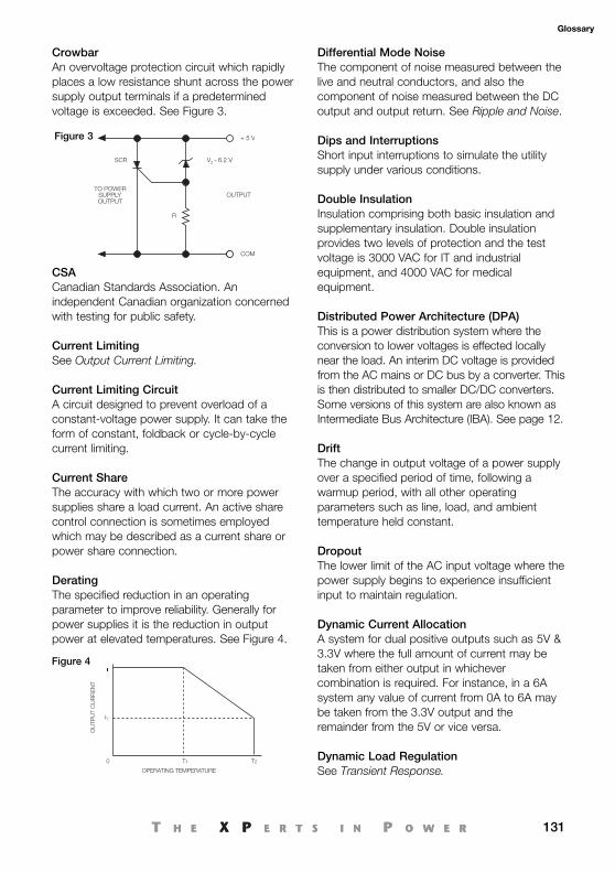
131
Glossary
CrowbarAn overvoltage protection circuit which rapidlyplaces a low resistance shunt across the powersupply output terminals if a predeterminedvoltage is exceeded. See Figure 3.
CSACanadian Standards Association. Anindependent Canadian organization concernedwith testing for public safety.
Current LimitingSee Output Current Limiting.
Current Limiting CircuitA circuit designed to prevent overload of aconstant-voltage power supply. It can take theform of constant, foldback or cycle-by-cyclecurrent limiting.
Current ShareThe accuracy with which two or more powersupplies share a load current. An active sharecontrol connection is sometimes employedwhich may be described as a current share orpower share connection.
DeratingThe specified reduction in an operatingparameter to improve reliability. Generally forpower supplies it is the reduction in outputpower at elevated temperatures. See Figure 4.
Differential Mode NoiseThe component of noise measured between thelive and neutral conductors, and also thecomponent of noise measured between the DCoutput and output return. See Ripple and Noise.
Dips and InterruptionsShort input interruptions to simulate the utilitysupply under various conditions.
Double InsulationInsulation comprising both basic insulation andsupplementary insulation. Double insulationprovides two levels of protection and the testvoltage is 3000 VAC for IT and industrialequipment, and 4000 VAC for medicalequipment.
Distributed Power Architecture (DPA)This is a power distribution system where theconversion to lower voltages is effected locallynear the load. An interim DC voltage is providedfrom the AC mains or DC bus by a converter. Thisis then distributed to smaller DC/DC converters.Some versions of this system are also known asIntermediate Bus Architecture (IBA). See page 12.
DriftThe change in output voltage of a power supplyover a specified period of time, following awarmup period, with all other operatingparameters such as line, load, and ambienttemperature held constant.
DropoutThe lower limit of the AC input voltage where thepower supply begins to experience insufficientinput to maintain regulation.
Dynamic Current AllocationA system for dual positive outputs such as 5V &3.3V where the full amount of current may betaken from either output in whichevercombination is required. For instance, in a 6Asystem any value of current from 0A to 6A maybe taken from the 3.3V output and theremainder from the 5V or vice versa.
Dynamic Load RegulationSee Transient Response.
T10 T2
I1
OU
TPU
T C
UR
RE
NT
OPERATING TEMPERATURE
Figure 4
OUTPUT
R
TO POWER SUPPLY OUTPUT
+ 5 V
Vz = 6.2 V SCR
COM
Figure 3
Glossary_120510.qxp:Layout 1 21/6/10 09:54 Page 131
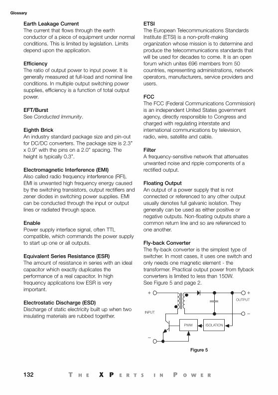
132
Glossary
Earth Leakage CurrentThe current that flows through the earthconductor of a piece of equipment under normalconditions. This is limited by legislation. Limitsdepend upon the application.
EfficiencyThe ratio of output power to input power. It isgenerally measured at full-load and nominal lineconditions. In multiple output switching powersupplies, efficiency is a function of total outputpower.
EFT/BurstSee Conducted Immunity.
Eighth BrickAn industry standard package size and pin-outfor DC/DC converters. The package size is 2.3”x 0.9” with the pins on a 2.0” spacing. Theheight is typically 0.3”.
Electromagnetic Interference (EMI)Also called radio frequency interference (RFI),EMI is unwanted high frequency energy causedby the switching transistors, output rectifiers andzener diodes in switching power supplies. EMIcan be conducted through the input or outputlines or radiated through space.
EnablePower supply interface signal, often TTLcompatible, which commands the power supplyto start up one or all outputs.
Equivalent Series Resistance (ESR)The amount of resistance in series with an idealcapacitor which exactly duplicates theperformance of a real capacitor. In highfrequency applications low ESR is veryimportant.
Electrostatic Discharge (ESD)Discharge of static electricity built up when twoinsulating materials are rubbed together.
ETSIThe European Telecommunications StandardsInstitute (ETSI) is a non-profit-makingorganization whose mission is to determine andproduce the telecommunications standards thatwill be used for decades to come. It is an openforum which unites 696 members from 50countries, representing administrations, networkoperators, manufacturers, service providers andusers.
FCCThe FCC (Federal Communications Commission)is an independent United States governmentagency, directly responsible to Congress andcharged with regulating interstate andinternational communications by television,radio, wire, satellite and cable.
FilterA frequency-sensitive network that attenuatesunwanted noise and ripple components of arectified output.
Floating OutputAn output of a power supply that is notconnected or referenced to any other outputusually denotes full galvanic isolation. Theygenerally can be used as either positive ornegative outputs. Non-floating outputs share acommon return line and so are referenced toone another.
Fly-back ConverterThe fly-back converter is the simplest type ofswitcher. In most cases, it uses one switch andonly needs one magnetic element - thetransformer. Practical output power from flybackconverters is limited to less than 150W. See Figure 5 and page 2.
PWM ISOLATION
OUTPUT
INPUT
Figure 5
Glossary_120510.qxp:Layout 1 21/6/10 09:54 Page 132
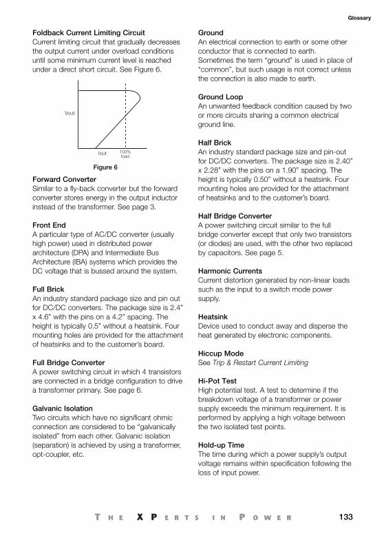
133
Glossary
Foldback Current Limiting CircuitCurrent limiting circuit that gradually decreasesthe output current under overload conditionsuntil some minimum current level is reachedunder a direct short circuit. See Figure 6.
Forward ConverterSimilar to a fly-back converter but the forwardconverter stores energy in the output inductorinstead of the transformer. See page 3.
Front EndA particular type of AC/DC converter (usuallyhigh power) used in distributed powerarchitecture (DPA) and Intermediate BusArchitecture (IBA) systems which provides theDC voltage that is bussed around the system.
Full BrickAn industry standard package size and pin outfor DC/DC converters. The package size is 2.4”x 4.6” with the pins on a 4.2” spacing. Theheight is typically 0.5” without a heatsink. Fourmounting holes are provided for the attachmentof heatsinks and to the customer’s board.
Full Bridge ConverterA power switching circuit in which 4 transistorsare connected in a bridge configuration to drivea transformer primary. See page 6.
Galvanic IsolationTwo circuits which have no significant ohmicconnection are considered to be “galvanicallyisolated” from each other. Galvanic isolation(separation) is achieved by using a transformer,opt-coupler, etc.
GroundAn electrical connection to earth or some otherconductor that is connected to earth.Sometimes the term “ground” is used in place of“common”, but such usage is not correct unlessthe connection is also made to earth.
Ground LoopAn unwanted feedback condition caused by twoor more circuits sharing a common electricalground line.
Half BrickAn industry standard package size and pin-outfor DC/DC converters. The package size is 2.40” x 2.28” with the pins on a 1.90” spacing. Theheight is typically 0.50” without a heatsink. Four mounting holes are provided for the attachmentof heatsinks and to the customer’s board.
Half Bridge ConverterA power switching circuit similar to the fullbridge converter except that only two transistors(or diodes) are used, with the other two replaced by capacitors. See page 5.
Harmonic CurrentsCurrent distortion generated by non-linear loadssuch as the input to a switch mode powersupply.
HeatsinkDevice used to conduct away and disperse theheat generated by electronic components.
Hiccup ModeSee Trip & Restart Current Limiting
Hi-Pot TestHigh potential test. A test to determine if thebreakdown voltage of a transformer or powersupply exceeds the minimum requirement. It isperformed by applying a high voltage betweenthe two isolated test points.
Hold-up TimeThe time during which a power supply’s outputvoltage remains within specification following theloss of input power.
Vout
Iout 100%load
Figure 6
Glossary_120510.qxp:Layout 1 21/6/10 09:54 Page 133
134
Glossary
Hot SwapRedundant units which may be removed andreplaced without the need to power downequipment.
I2C BusInter Integrated Circuit BUS is a serial BUSdeveloped by Philips Semiconductor in the 1980s.Widely used in power management systems. Seepage 60.
IECInternational Electrotechnical Commission.
Induced NoiseNoise generated in a circuit by a varyingmagnetic field produced by another circuit.
InhibitPower supply interface signal, often TTLcompatible, which commands the power supplyto shut down one or all outputs.
Input Line FilterA low-pass or band-reject filter at the input of apower supply which reduces line noise fed tothe supply. This filter may be external to thepower supply.
Input Voltage RangeThe high and low input voltage limits withinwhich a power supply or DC/DC convertermeets its specifications.
Inrush CurrentThe peak instantaneous input current drawn bya power supply at turn-on.
Inrush Current LimitingA circuit which limits the inrush current duringturn-on of a power supply.
Intermediate Bus Architecture (IBA)See Distributed Power Architecture (DPA).
InverterA power converter which changes DC inputpower into AC output power.
IsolationThe electrical separation between input andoutput of a power supply by means of thepower transformer. The isolation resistance(normally in mega ohms) and the isolationcapacitance (normally in pico farads) aregenerally specified and are a function ofmaterials and spacings employed throughoutthe power supply.
Isolation VoltageThe maximum AC or DC voltage that may beapplied for a short, defined duration from inputto output and/or chassis of a power supply.
KETIKorean Electrical Testing Institute. Certificationbody for safety and EMC in Korea.
Line Frequency RegulationThe variation of an output voltage caused by achange in line input frequency, with all otherfactors held constant. This effect is negligible inswitching and linear power supplies.
Line RegulationThe variation of an output voltage due to achange in the input voltage, with all other factorsheld constant. Line regulation is expressed as themaximum percentage change in output voltage asthe input voltage is varied over its specified range.
Linear RegulatorA common voltage-stabilization technique inwhich the control device (usually a transistor) isplaced in series or parallel with the powersource to regulate the voltage across the load.The term 'linear' is used because the voltagedrop across the control device is variedcontinuously to dissipate unused power.
Load RegulationVariation of the output voltage due to a changein the output load, with all other factors heldconstant. It is expressed as a percentage of thenominal DC output voltage.
Local SensingUsing the output terminals of the power supplyas sense points for voltage regulation.
Glossary_120510.qxp:Layout 1 21/6/10 09:54 Page 134
135
Glossary
Logic EnableThe ability to turn a power supply on and offwith a TTL signal. A logic low generally turns thesupply off; logic high turns it on.
Long Term StabilityPower supply output voltage change due to timewith all other factors held constant. This isexpressed in percent and is a function ofcomponent ageing.
Magnetic AmplifierA magnetic device used to improve the crossregulation of multiple output AC/DC converters.
MarginingAdjusting a power supply output voltage up ordown from its nominal setting in order to verifysystem performance. This is usually doneelectrically by a system-generated control signal.
Minimum LoadThe minimum load current/power that must bedrawn from the power supply in order for thesupply to meet its performance specifications.Less commonly, a minimum load is required toprevent the power supply from failing.
ModularA physically descriptive term used to describe apower supply made up of a number of separatesubsections, such as an input module, powermodule, or filter module.
MOSFETMetal oxide semiconductor field effect transistor.The device of choice for the main switch inmany switch mode power supplies, havingmuch better switching characteristics thanbipolar transistors.
MTBFMean time between failures. The failure rate of asystem or component, expressed in hours,established by the actual operation(demonstrated MTBF) or calculated from aknown standard such as MIL-HDBK-217.
NoiseNoise is the aperiodic, random component ofundesired deviations in output voltage. Usuallyspecified in combination with ripple. See PARDand Ripple.
Nominal ValueThe stated or objective value for a quantity, suchas output voltage, which may not be the actualvalue measured.
Off-line Power SupplyA power supply which operates off the AC linedirectly, without using a power transformer priorto rectification and filtering.
Open FrameA power supply with no external metal chassis;the power supply is provided to the end useressentially as a printed circuit board whichprovides mechanical support as well assupporting the components and makingelectrical connections.
Operational InsulationOperational insulation is needed for the correctoperation of the equipment, but does notprotect against electric shock. Operationalinsulation provides no levels of protection andtypically the test voltage is ≤ 500 VDC.
Operating Temperature RangeSee Temperature Range, Operating.
Operational Power SupplyA power supply with a high open loop gainregulator which acts like an operational amplifierand can be programmed with passivecomponents.
Output Current LimitingAn output protection feature which limits theoutput current to a predetermined value in orderto prevent damage to the power supply or theload under overload conditions. The supply isautomatically restored to normal operationfollowing removal of the overload.
Glossary_120510.qxp:Layout 1 21/6/10 09:54 Page 135
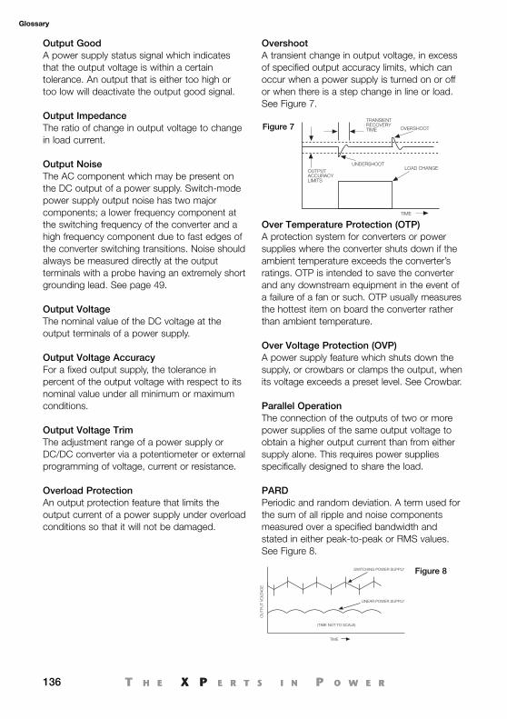
136
Glossary
Output GoodA power supply status signal which indicatesthat the output voltage is within a certaintolerance. An output that is either too high ortoo low will deactivate the output good signal.
Output ImpedanceThe ratio of change in output voltage to changein load current.
Output NoiseThe AC component which may be present onthe DC output of a power supply. Switch-modepower supply output noise has two majorcomponents; a lower frequency component atthe switching frequency of the converter and ahigh frequency component due to fast edges ofthe converter switching transitions. Noise shouldalways be measured directly at the outputterminals with a probe having an extremely shortgrounding lead. See page 49.
Output VoltageThe nominal value of the DC voltage at theoutput terminals of a power supply.
Output Voltage AccuracyFor a fixed output supply, the tolerance inpercent of the output voltage with respect to itsnominal value under all minimum or maximumconditions.
Output Voltage TrimThe adjustment range of a power supply orDC/DC converter via a potentiometer or externalprogramming of voltage, current or resistance.
Overload ProtectionAn output protection feature that limits theoutput current of a power supply under overloadconditions so that it will not be damaged.
OvershootA transient change in output voltage, in excessof specified output accuracy limits, which canoccur when a power supply is turned on or offor when there is a step change in line or load.See Figure 7.
Over Temperature Protection (OTP)A protection system for converters or powersupplies where the converter shuts down if theambient temperature exceeds the converter’sratings. OTP is intended to save the converterand any downstream equipment in the event ofa failure of a fan or such. OTP usually measuresthe hottest item on board the converter ratherthan ambient temperature.
Over Voltage Protection (OVP)A power supply feature which shuts down thesupply, or crowbars or clamps the output, whenits voltage exceeds a preset level. See Crowbar.
Parallel OperationThe connection of the outputs of two or morepower supplies of the same output voltage toobtain a higher output current than from eithersupply alone. This requires power suppliesspecifically designed to share the load.
PARDPeriodic and random deviation. A term used forthe sum of all ripple and noise componentsmeasured over a specified bandwidth andstated in either peak-to-peak or RMS values.See Figure 8.
OU
TPU
T V
OLT
AG
E
LINEAR POWER SUPPLY
(TIME NOT TO SCALE)
SWITCHING POWER SUPPLY
TIME
Figure 8
LOAD CHANGE
TRANSIENTRECOVERYTIME
OUTPUTACCURACYLIMITS
OVERSHOOT
UNDERSHOOT
TIME
Figure 7
Glossary_120510.qxp:Layout 1 21/6/10 09:54 Page 136
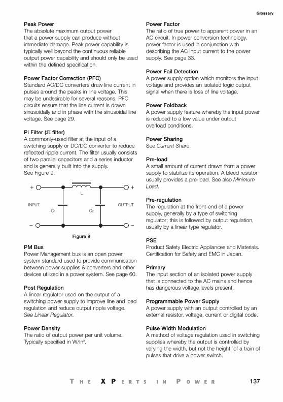
137
Glossary
Peak PowerThe absolute maximum output power that a power supply can produce withoutimmediate damage. Peak power capability istypically well beyond the continuous reliableoutput power capability and should only be usedwithin the defined specification.
Power Factor Correction (PFC)Standard AC/DC converters draw line current inpulses around the peaks in line voltage. Thismay be undesirable for several reasons. PFCcircuits ensure that the line current is drawnsinusoidally and in phase with the sinusoidal linevoltage. See page 29.
Pi Filter (π filter)A commonly-used filter at the input of aswitching supply or DC/DC converter to reducereflected ripple current. The filter usually consistsof two parallel capacitors and a series inductorand is generally built into the supply. See Figure 9.
PM BusPower Management bus is an open powersystem standard used to provide communicationbetween power supplies & converters and otherdevices utilized in a power system. See page 60.
Post RegulationA linear regulator used on the output of aswitching power supply to improve line and loadregulation and reduce output ripple voltage. See Linear Regulator.
Power DensityThe ratio of output power per unit volume.Typically specified in W/In3.
Power FactorThe ratio of true power to apparent power in anAC circuit. In power conversion technology,power factor is used in conjunction withdescribing the AC input current to the powersupply. See page 33.
Power Fail DetectionA power supply option which monitors the inputvoltage and provides an isolated logic outputsignal when there is loss of line voltage.
Power FoldbackA power supply feature whereby the input poweris reduced to a low value under output overload conditions.
Power SharingSee Current Share.
Pre-loadA small amount of current drawn from a powersupply to stabilize its operation. A bleed resistorusually provides a pre-load. See also MinimumLoad.
Pre-regulationThe regulation at the front-end of a powersupply, generally by a type of switchingregulator; this is followed by output regulation,usually by a linear type regulator.
PSEProduct Safety Electric Appliances and Materials.Certification for Safety and EMC in Japan.
PrimaryThe input section of an isolated power supplythat is connected to the AC mains and hencehas dangerous voltage levels present.
Programmable Power SupplyA power supply with an output controlled by anexternal resistor, voltage, current or digital code.
Pulse Width ModulationA method of voltage regulation used in switchingsupplies whereby the output is controlled byvarying the width, but not the height, of a train ofpulses that drive a power switch.
OUTPUTINPUTC1 C2
L
Figure 9
Glossary_120510.qxp:Layout 1 21/6/10 09:54 Page 137
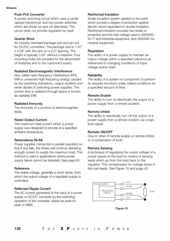
138
Glossary
Push-Pull ConverterA power switching circuit which uses a centertapped transformer and two power switcheswhich are driven on and off alternately. Thiscircuit does not provide regulation by itself.
Quarter BrickAn industry standard package size and pin-outfor DC/DC converters. The package size is 1.45”x 2.28” with the pins on a 2.0” spacing. Theheight is typically 0.50” without a heatsink. Fourmounting holes are provided for the attachmentof heatsinks and to the customer’s board.
Radiated Electromagnetic InterferenceAlso called radio frequency interference (RFI),EMI is unwanted high-frequency energy causedby the switching transistors, output rectifiers andzener diodes in switching power supplies. Theportion that is radiated through space is knownas radiated EMI.
Radiated ImmunityThe immunity of a product to electromagneticfields.
Rated Output CurrentThe maximum load current which a powersupply was designed to provide at a specifiedambient temperature.
Redundancy (N+M)Power supplies connected in parallel operation sothat if one fails, the others will continue deliveringenough current to supply the maximum load. Thismethod is used in applications where powersupply failure cannot be tolerated. See page 63.
ReferenceThe stable voltage, generally a zener diode, fromwhich the output voltage of a regulated supply iscontrolled.
Reflected Ripple CurrentThe AC current generated at the input of a powersupply or DC/DC converter by the switchingoperation of the converter, stated as peak-to-peak or RMS.
Reinforced InsulationSingle insulation system applied to live partswhich provide a degree of protection againstelectric shock equivalent to double insulation.Reinforced insulation provides two levels ofprotection and the test voltage used is 3000VACfor IT and industrial equipment, and 4000VAC formedical equipment.
RegulationThe ability of a power supply to maintain anoutput voltage within a specified tolerance asreferenced to changing conditions of inputvoltage and/or load.
ReliabilityThe ability of a system or component to performits required functions under stated conditions fora specified amount of time.
Remote EnableThe ability to turn on electrically the output of apower supply from a remote location.
Remote InhibitThe ability to electrically turn off the output of apower supply from a remote location via a logiclevel signal.
Remote ON/OFFOne or other of remote enable or remote inhibit,or a combination of both.
Remote SensingA technique of regulating the output voltage of apower supply at the load by means of sensingleads which go from the load back to theregulator. This compensates for voltage drops inthe load leads. See Figure 10 and page 42.
POWER SUPPLY
LOAD
OUT
SENSE
SENSE
OUT
REGULATORCIRCUIT
Figure 10
Glossary_120510.qxp:Layout 1 21/6/10 09:54 Page 138
139
Glossary
ResolutionFor an adjustable supply, the smallest change inoutput voltage that can be realized by theadjustment.
Resonant ConverterA class of power converter topology whichreduces the level of switching losses by forcingeither zero voltage across, or zero currentthrough the switching device when it is turnedon or off.
ReturnThe name for the common terminal of theoutput of a power supply; it carries the returncurrent for the outputs.
Reverse Voltage ProtectionA feature which protects a power supply againsta reverse voltage applied at the input or outputterminals.
RFISee Radiated Electromagnetic Interference.
Ripple and NoiseThe magnitude of AC voltage on the output of apower supply, expressed in millivolts peak-to-peak or RMS, at a specified bandwidth. This isthe result of feed through of the rectified linefrequency, internal switching transients and otherrandom noise. See also PARD & Noise.
Rise TimeThe time required for the voltage in a switchingelectronic circuit to rise from 10% to 90% of itsnominal final value.
Safety ApprovalsThird party or agency approvals to internationallyrecognized safety standards.
Safety GroundA conductive path to earth that is designed toprotect persons from electrical shock byshunting away any dangerous currents thatmight occur due to malfunction or accident.
SecondaryThe output section of an isolated power supplywhich is isolated from the AC mains andspecially designed for safety of personnel whomight be working with power on the system.
SELVSafety extra low voltage. A term generallydefined by the regulatory agencies as thehighest voltage that can be contacted by aperson and not cause injury. It is oftenspecifically defined as 42.4 VAC or 60 VDC.
SequencingThe desired order of activation of the outputs ofa multiple output power supply.
Shock and VibrationA specification requirement for which a powersupply is designed or tested to withstand, such as20 g shock for 11 milliseconds and 10 g randomvibration for 2 hours over a 2-2000 Hz bandwidth.
Short Circuit ProtectionA feature which limits the output current of a powersupply under short circuit conditions so that thesupply will not be damaged.
SignalsOutput interface, often at TTL level, of variousoperational conditions such as power fail andDC OK.
Sixteenth BrickAn industry standard package size and pin-outfor DC/DC converters. The package size is 1.3”x 0.9” with the pins on a 1.1” spacing. Theheight is typically less than 0.4”.
Soft StartA technique for gradually activating a powersupply circuit when the power supply is firstturned on. This technique is generally used toprovide a gradual rise in output voltages and tolimit inrush current.
Standby CurrentThe input current drawn by a power supplywhen shut down by a control input (remoteinhibit) or under no load.
Glossary_120510.qxp:Layout 1 21/6/10 09:54 Page 139
140
Glossary
Start-up Rise TimeThe time between the output voltage starting torise and reaching the desired level.
Start-up Time (Start-up Delay)Time between the application of input voltageand the output voltage being within regulation.
Supplementary InsulationIndependent insulation applied in addition tobasic insulation in order to provide protectionagainst electric shock in the event of a failure ofbasic insulation. Supplementary insulationprovides one level of protection and has a testvoltage of 1500 VAC.
Surface Mount Technology (SMT)A space-saving technique whereby special lead-less components are soldered onto the surfaceof a PCB rather than into holes in a PCB. Theparts are smaller than their leaded versions andPCB area is saved.
SurgePart of the conducted immunity suite of tests,designed to simulate a nearby lightning strike.
Switching FrequencyThe rate at which the DC voltage is switched onand off during the pulse width modulationprocess in a switching power supply.
Synchronous Rectifiers or RectificationA circuit arrangement where the output rectifierdiodes of a power supply are replaced withactive switches such as MOSFETs. The switchesare turned on and off under control and act asrectifiers. This results in considerably lowerlosses in the output stage and subsequentlymuch higher efficiency. They are particularlyuseful with low voltage outputs.
Temperature CoefficientThe average percent change in output voltageper degree centigrade change in ambienttemperature over a specified temperature range.
Temperature DeratingReducing the output power of a power supplywith increasing temperature to maintain reliableoperation.
Temperature Range, OperatingThe range of ambient or case temperatures withinwhich a power supply may be safely operated andmeet its specifications.
Temperature Range, StorageThe range of ambient temperatures within which anon-operating power supply may be safely storedwith no degradation of its subsequent operation.
Thermal ProtectionSee Over Temperature Protection.
TopologyThe design type of a converter, indicative of theconfiguration of switching transistors, utilizationof the transformer, and type of filtering.Examples of topologies are fly-back, forward,half-bridge, full-bridge, and resonant.
TrackingA characteristic of a dual or other multiple outputpower supply whereby one or more outputs followanother output with changes in line, load andtemperature, so that each maintains the sameproportional output voltage, within specifiedtracking tolerance, with respect to common.
Transient ResponseThe time required for the output voltage of apower supply to settle within specified outputaccuracy limits following a step change in outputload current or a step change in input voltage.
Trip & Restart Current LimitingCurrent limiting circuit which switches off theoutput when an overload condition is reached.The unit will then try to restart periodically untilthe overload is removed.
TUVTUV Rheinland Product Safety Group. Anindependent German organization which testsproducts for safety.
Glossary_120510.qxp:Layout 1 21/6/10 09:54 Page 140
141
Glossary
• Prefix CodesPrefix Multipliers
Prefix Symbol Multiplierexa- E 1,000,000,000,000,000,000peta- P 1,000,000,000,000,000tera- T 1,000,000,000,000giga- G 1,000,000,000mega- M 1,000,000kilo- k 1,000hecto- h 100deca- da 10deci- d 0.1centi- c 0.01milli- m 0.001micro- μ 0.000 001nano- n 0.000 000 001pico- p 0.000 000 000 001femto- f 0.000 000 000 000 001atto- a 0.000 000 000 000 000 001
ULUnderwriter’s Laboratories Incorporated. Anindependent, U.S. organization which testsproducts for safety.
UndershootA transient change in output voltage, belowoutput accuracy limits, which can occur when apower supply is turned on or off, or when thereis a step change in line or load. See Overshoot.
Universal InputA power supply's ability to accept a wide inputvoltage range (90VAC to 264VAC) without theselection of input range, either manually orelectronically (as in auto-ranging input).
UPSUninterruptible power supply. A power supplythat continues to supply power during a loss ofAC input power. This is accomplished by meansof a back-up battery and a DC/AC inverter orDC/DC converter.
Under Voltage Lock Out (UVLO)A protection system for power converters wherethe converter is deliberately shut down if theinput voltage drops below a pre-defined level.Some hysteresis is usually present to preventthe converter oscillating on and off. UVLO isusually needed with battery systems where thevoltage decreases gradually with time ratherthan turning off quickly.
VDEVerband Deutsche Elektrotechniker. A Germanorganization which tests equipment for publicsafety and emitted noise.
Voltage BalanceThe percentage difference in magnitudebetween the two output voltages of a dualoutput power supply where the voltages haveequal nominal values with opposite polarities.
Warm-up DriftThe initial change in output voltage of a powersupply from turn-on until it reaches thermalequilibrium at nominal line, full load, 25°Cambient temperature.
Warm-up TimeThe time required, after initial turn-on, for apower supply to meet its performancespecifications.
Zero Current Switching (ZCS)See Resonant Converter.
Zero Voltage Switching (ZVS)See Resonant Converter.
Glossary_120510.qxp:Layout 1 21/6/10 09:54 Page 141
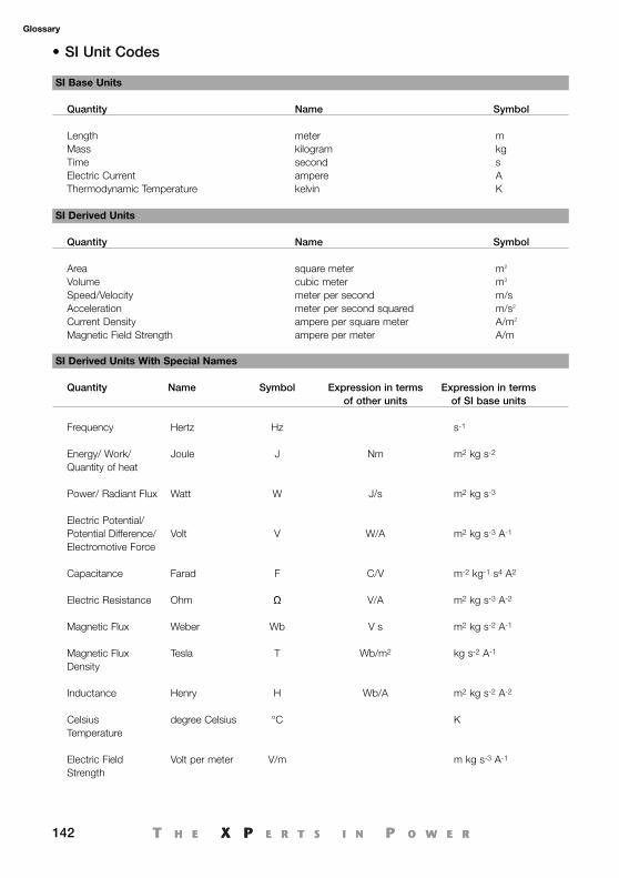
• SI Unit Codes
SI Base Units
Quantity Name Symbol
Length meter mMass kilogram kgTime second sElectric Current ampere AThermodynamic Temperature kelvin K
SI Derived Units
Quantity Name Symbol
Area square meter m2
Volume cubic meter m3
Speed/Velocity meter per second m/sAcceleration meter per second squared m/s2
Current Density ampere per square meter A/m2
Magnetic Field Strength ampere per meter A/m
SI Derived Units With Special Names
Quantity Name Symbol Expression in terms Expression in termsof other units of SI base units
Frequency Hertz Hz s-1
Energy/ Work/ Joule J Nm m2 kg s-2
Quantity of heat
Power/ Radiant Flux Watt W J/s m2 kg s-3
Electric Potential/ Potential Difference/ Volt V W/A m2 kg s-3 A-1
Electromotive Force
Capacitance Farad F C/V m-2 kg-1 s4 A2
Electric Resistance Ohm Ω V/A m2 kg s-3 A-2
Magnetic Flux Weber Wb V s m2 kg s-2 A-1
Magnetic Flux Tesla T Wb/m2 kg s-2 A-1
Density
Inductance Henry H Wb/A m2 kg s-2 A-2
Celsius degree Celsius °C KTemperature
Electric Field Volt per meter V/m m kg s-3 A-1
Strength
Glossary
142
Glossary_120510.qxp:Layout 1 21/6/10 09:54 Page 142
143
IndexTerm Page Term PageAC Generator 13AC Motor Load 33AC OK 55AC Power Sources 13AC Resistive Load 35Active Power Factor Correction (PFC) 30Active Power Sharing 62Apparent Power 32Baseplate Cooling 71Batteries 19Battery Charging 20-21Boost Converter 9Buck Converter 8California Energy Commission (CEC) 105CE Marking 97-98Circuit Breakers 25/53Class I Systems 83Class II Systems 84Common Mode Noise 92Conducted Emissions 103Conducted Immunity Phenomena 95Conducted Noise 91/93Constant Current Limit 53Constant Power Limit 52Control Interfaces 56Controller Area Network (CAN) Bus 60Convection Cooling 67Cooling Power Modules 70Cooling Power Supplies 67Creative Mechanical Design 113Cross Regulation 41Crow-bar 54Current Share 57Custom Power 126-128DC OK 56DC Power Sources 18Declaration of Conformity (DofC) 98Defense and Avionics EMC Standards 98-103Delta Connection 16Differential Mode Noise 92Digital Communication Interfaces 59Digital Signals and Controls 123-125Distributed Power Architecture 11Earth Leakage Current 83/116Earthing / Grounding 38Earthing for Safety 39-40Efficiency 67/117Electrical Safety 82Electromagnetic Compatibility (EMC) 91/119EMC Filtering 94Emissions 91
Enable 56Energy Efficiency 107-108Energy Independence & Security (EISA) 104Energy Related Products (ErP) 98Energy Star 105Energy Star Products 108ErP Directive 105Factors Affecting Reliability 77Failure Rate 75/78Filter Selection 94Fold-back Current Limit 53Forced Cooling 67Forward Converter 3Frequency 14Full Bridge Converter 6Fuse Characteristics 24/53Glossary 129Green IT Systems 114Ground Resistivity 39Half Bridge & Full Bridge Converters 5Harmonic Distortion 28Harmonics 28-29Harmonics effect on Power Factor 36Heatsink Calculations 73Hiccup Mode 51High Efficiency Power Supplies 109-114High Peak Loads 43-44Immunity 95-96Inhibit 56Input Characteristics 115Input Current Protection 22Input Voltage Protection 22/26Inrush Current 23/116Insulation 82Insulation Types 89Inter Integrated Circuit (I2C) Bus 60Isolated Fly-back Converter 2Isolated Signals Output 59Leakage Current 87LED Drivers 47Legislation 81Line Regulation 41Linear Power Supplies 10Lithium 20Load Regulation 41Low System Power Factor 37Low Voltage Directive (LVD) 97Manufacturing Methods 79Marking Requirements 106Matrix Configuration (LED's) 48Measurement Technique 106
index_120510.qxp:Layout 1 21/6/10 09:57 Page 143
144
Medical Power Supplies 120-122Medical Safety 84-88Methods of Measurements 93Minimum Loads 117MTBF 75Multiple Channel Configuration (LED's) 48N+M Redundancy 63Nickel Cadmium and Nickel Metal Hydride 19No Load Power Consumption 104Nominal Voltage 17Open Collector Signals 59Open Drain Signals 59Opto-coupler Signal Output 59Output Accuracy 117Output Characteristics 115Output Margining 58Output Protection 51Output Regulation 41Output Ripple & Noise 117Overload Protection 51Over Voltage Protection (OVP) 54/55Parallel Configuration (LED's) 48Parallel Operation 61Passive Power Factor Correction (PFC) 29PFC Boost Converter 10Power Distribution 15Power Fail (PF) 55Power Good 56Powering Light Emitting Diodes (LED's) 45-49Power Losses 64Power Management (PM) Bus 60Power Share 57Power Sources 13-18Power Supply Datasheets 115-119Power Supply Safety 81Prototype Testing 79Push-Pull Converter 7Radiated Immunity Phenomena 95Radiated Noise 92/93Reactive Power 32Real and Apparent Power 31Real Power 31Redundant Operation 63Relay Signal Output 59Reliability 75Reliability, Temperature & Cooling 118Remote Sense 42/117Reverse Polarity Protection 27Ripple and Noise 49-50Sealed Military Systems 114Series Configuration (LED's) 48
Series Operation 61Service Life 76Single-phase Voltages & Frequency 17Single Wire Parallel 57Sizing of Fuses & Circuit Breakers 24Standards 92/95-96Star or Wye Connection 16Status Signals and Controls 55Summary of Limits 105Switch Mode Power Supplies (SMPS) 1System Cooling Fan Selection 64-66System Reliability 80System Reset 56Terminology 75Three-phase AC 15Topologies (Power Supply) 2Topologies (Signals) 58Transient Load Response 43Trip and Restart Mode 51TTL Compatible Signals 58Two Transistor Forward Converter 4Valve Regulated Lead Acid 19Voltage Adjust 57Voltage Programming 57
IndexTerm Page Term Page
index_120510.qxp:Layout 1 21/6/10 09:57 Page 144
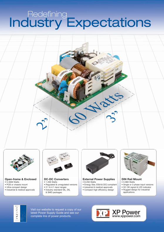
Open-frame & Enclosed• 5-3000 Watts• PCB or chassis mount• Ultra-compact design• Industrial & medical approvals
DC-DC Converters• 1-200 Watts• Regulated & unregulated versions• 2:1 & 4:1 input ranges• Industry standard SIL, DIL& SMD packages
External Power Supplies• 8-250 Watts• Energy Star, EISA & CEC compliant• Industrial & medical approvals• Compact high efficiency design
DIN Rail Mount• 5-960 Watts• Single or 3 phase input versions• DC OK signal & LED indicator• Rugged design for industrialapplications
RedefiningIndustry Expectations
Visit our website to request a copy of ourlatest Power Supply Guide and see ourcomplete line of power products.
North American HQ
XP Power990 Benecia Avenue, Sunnyvale, CA 94085Phone : +1 (408) 732-7777Fax : +1 (408) 732-2002Email : [email protected]
North American Sales OfficesToll Free...................................+1 (800) 253-0490Central Region ........................+1 (972) 578-1530Eastern Region .....................+1 (973) 658-8001Western Region.......................+1 (408) 732-7777
European HQ
XP PowerHorseshoe Park, Pangbourne,Berkshire, RG8 7JWPhone : +44 (0)118 984 5515Fax : +44 (0)118 984 3423Email : [email protected]
European Sales OfficesAustria ..................................+41 (0)56 448 90 80Belgium...............................+33 (0)1 45 12 31 15Denmark ....................................+45 43 42 38 33Finland .................................+46 (0)8 555 367 01France ................................+33 (0)1 45 12 31 15Germany .............................+49 (0)421 63 93 3 0Italy ..........................................+39 039 2876027Netherlands.........................+49 (0)421 63 93 3 0Norway ......................................+47 63 94 60 18Sweden............................... +46 (0)8 555 367 00Switzerland.......................... +41 (0)56 448 90 80United Kingdom ..................+44 (0)118 984 5515
Asian HQXP Power401 Commonwealth Drive, Haw Par Technocentre, Lobby B #02-02Singapore 149598Phone : +65 6411 6900Fax : +65 6741 8730Email : [email protected] : www.xppowerchina.com / www.xppower.com
Asian Sales OfficesShanghai ................................. +86 21 51388389Singapore.................................... +65 6411 6902
Distributors
Australia ....................................+61 2 9809 5022 AmtexBalkans .....................................+386 1 583 7930 ElbacompCzech Rep. .............................+420 235 366 129 Vums PowerpragCzech Rep. .............................+420 539 050 630 Koala ElektronikEstonia ..........................................+372 6228866 ElgertaGreece ....................................+30 210 240 1961 ADEM ElectronicsIsrael ..........................................+972 9 7498777 AppletecJapan........................................+81 48 864 7733 BellnixKorea ........................................+82 31 422 8882 HanpowerLatvia...........................................+371 67501005 CaroLithuania.....................................+370 5 2652683 ElgertaPoland........................................+48 22 8627500 GammaPortugal ...................................+34 93 263 33 54 VencoRussia .....................................+7 (495)234 0636 ProsoftRussia .....................................+7 (812)325 5115 GammaSouth Africa ..............................+27 11 453 1910 VepacSpain .......................................+34 93 263 33 54 VencoTaiwan........................................+886 3 3559642 Fullerton PowerTurkey .....................................+90 212 465 7199 EMPA
Global Catalog Distributors
Americas...................................................Newark newark.comEurope & Asia.............................................Farnell farnell.comChina ......................................Premier Electronics premierelectronics.com.cn
German HQ
XP PowerAuf der Höhe 2, D-28357Bremen, GermanyPhone : +49 (0)421 63 93 3 0Fax : +49 (0)421 63 93 3 10Email : [email protected]