Embed Size (px)
Citation preview
Article
Printable Metal-Polymer Conductors for HighlyStretchable Bio-Devices
Lixue Tang, Shiyu
Cheng, Luyao
Zhang, ..., Zhiwei
Huang, Xinghua
Shi, Xingyu Jiang
HIGHLIGHTSA straightforward method
for sintering liquid metal
particles with high
efficiency
Liquid metal can be
patterned on different
substrates with high
resolution
Low-cost, high-
throughput, stretchable
printed conductors can be
fabricated
Conductors are
biocompatible and have
potentials in implantable
electronics
Tang et al., iScience 4, 302–311June 29, 2018 ª 2018 TheAuthor(s).
https://doi.org/10.1016/
j.isci.2018.05.013
Article
Printable Metal-Polymer Conductorsfor Highly Stretchable Bio-DevicesLixue Tang,1,2 Shiyu Cheng,1,2 Luyao Zhang,1,2,3 Hanbing Mi,1,2 Lei Mou,1,2 Shuaijian Yang,2 Zhiwei Huang,2
Xinghua Shi,1,2 and Xingyu Jiang1,2,4,*
1Beijing EngineeringResearch Center forBioNanotechnology and CASKey Laboratory forBiomedical Effects ofNanomaterials andNanosafety, CAS Center forExcellence in Nanoscience,National Center forNanoScience andTechnology, No. 11Zhongguancun Beiyitiao,Beijing 100190, P. R. China
2University of ChineseAcademy of Sciences, 19 AYuquan Road, ShijingshanDistrict, Beijing 100049, P. R.China
3State Key Laboratory ofNonlinear Mechanics,Institute of Mechanics,Chinese Academy ofSciences, Beijing 100190, P.R. China
4Lead Contact
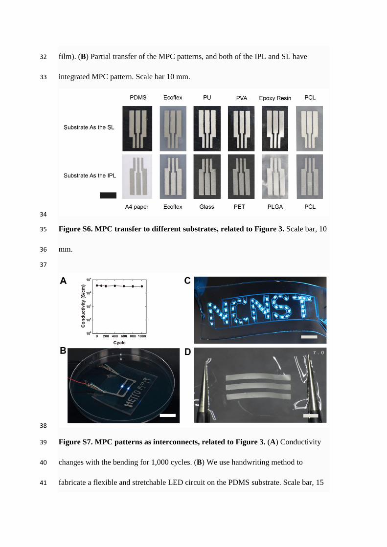
*Correspondence:[email protected]
https://doi.org/10.1016/j.isci.2018.05.013
SUMMARY
Stretchable, biocompatible devices can bridge electronics and biology. However, most stretchable
conductors for such devices are toxic, costly, and regularly break/degrade after several large defor-
mations. Herewe showprintable, highly stretchable, and biocompatiblemetal-polymer conductors by
casting and peeling off polymers from patterned liquid metal particles, forming surface-embedded
metal in polymeric hosts. Our printable conductors present good stretchability (2,316 S/cm at a strain
of 500%) and repeatability (DR/R <3% after 10,000 cycles), which can satisfy most electrical applica-
tions in extreme deformations. This strategy not only overcomes large surface tension of liquid metal
but also avoids the undesirable sintering of its particles by stress in deformations, such that stretch-
able conductors can form on various substrates with high resolution (15 mm), high throughput (�2,000
samples/hour), and low cost (one-quarter price of silver). We use these conductors for stretchable cir-
cuits, motion sensors, wearable glove keyboards, and electroporation of live cells.
INTRODUCTION
Fusion of electronics with biology and medicine demands electronic devices that are supple, stretchable,
and compatible with human tissues, such as the skin (Kim et al., 2011; Oh et al., 2016) and the brain (Kang
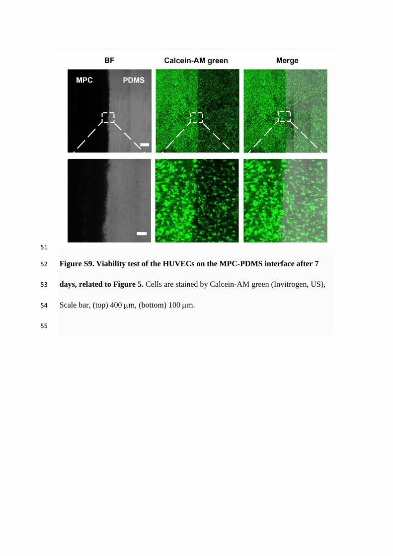
et al., 2016; Liu et al., 2015), especially in the fields of health monitoring and disease treatment (Chortos
et al., 2016; Sun et al., 2014; Jeong et al., 2015a). Flexible circuits are currently realized by depositing a
thin layer of metal like copper and gold on flexible substrates such as polyimide. To further endow such
flexible circuits with stretchability, wavy or serpentine structures are designed to counteract deformations
(Lou et al., 2017; Kim et al., 2008). The stretchability of these strategies is limited (about 150%), and the
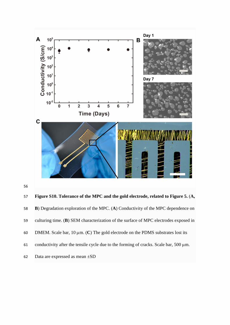
fabrication processes of such structures are often complicated. Another approach is developing conduc-
tive materials that could bear large deformations such as carbon nanomaterials, silver inks, and liquid
metals (LMs) (Kazem et al., 2017; Qi et al., 2015; Zheng et al., 2014; Matsuhisa et al., 2017; Tang et al.,
2014). Most of these materials are hard to be patterned with microstructures in large scale. Among these
materials, LMs, especially eutectic gallium indium alloy (EGaIn, melting point 15�C), stand out for their
excellent performances of high conductivity and unequaled stretchability (Dickey, 2017). Besides, EGaIn
is much less toxic (Lu et al., 2015) than other metals that may potentially be useful for these applications,
such as mercury (also liquid at room temperature) or silver (its nanowires can withstand stretch). However,
the huge surface tension (>400 mN/m) (Dickey, 2014) of LM impedes its direct patterning by using straight-
forward technologies such as stencil and ink-jet printing (Zheng et al., 2014; Wang et al., 2015), making its
patterning limited to very few substrates that can be wetted by LMs. In addition, such strategies have high
LM consumption (the thickness of the LM pattern is usually larger than 100 mm), which further limits their
wider applications. Another common method, injecting the LM into microfluidic channels or hollow wires,
can yield conductors with high stretchability (>1,000%). However, these methods cannot fabricate complex
conductive patterns that require the microfluidic channels or hollow wires to be continuous from the begin-
ning to end (Kubo et al., 2010; Zhu et al., 2013). By contrast, bottom-up approaches to fabricate LM into
particles is a good way to minimize the surface tension. Some reported strategies usually deposit a layer
of liquid metal particles (LMPs) (not conductive due to the oxide layer on the particles) on the surface of
elastomers and use a marker to mechanically sinter LMPs (break the oxide layer to release the conductive
LM) to obtain a desirable conductive pattern (Lin et al., 2015; Boley et al., 2015; Ren et al., 2016; Mohammed
and Kramer, 2017). However, conductive patterns fabricated by these strategies cannot bear large defor-
mations like stretching in practical applications, because stress in deformations will also sinter the LMPs in
regions where conductive patterns are not desirable, causing short circuit in the electronics. Besides, using
a marker to sinter the LMP to obtain electronics has low efficiency and low utilization of particles. These
strategies using LMPs are not applicable to mass-manufacturing.
302 iScience 4, 302–311, June 29, 2018 ª 2018 The Author(s).This is an open access article under the CC BY-NC-ND license (http://creativecommons.org/licenses/by-nc-nd/4.0/).
Here, we report printable and mass-manufacturable metal-polymer conductors (MPCs) by fabricating LM
into LMPs (liquid core-oxide shell structure), and embedding the patterned LMPs on the surface of poly-
mers by casting and peeling off steps, instead of using a marker or a nozzle, to result in microstructured,
conductive path. The theoretical calculation indicates that the stress on the particles during stripping is
much larger than the yield stress of gallium oxide, causing the release of the LM to form conductive paths.
We used screen printing or microfluidic patterning strategy to pattern any 2D MPC pattern on various sub-
strates in different thicknesses with high resolution (15 mm), high efficiency, and low cost. The printable
MPC is highly conductive (8 3 103 S/cm), robust, and stretchable, which can keep conductivity as high
as 2,316 S/cm at a strain of 500%. Because MPC patterns allow exposed LMs on the surface of polymer sub-
strates (instead of completely buried within polymers), electronic components could be easily mounted.
We used the printable MPC for highly stretchable circuits, motion sensors, wearable glove keyboards,
and electroporation of live cells because of its biocompatibility. This potentially widely applicable
approach will greatly increase the stretchability of electronic devices and sharply decrease the production
cost of printed electronics, which will significantly promote the development of wearable or implantable
electronic devices.
RESULTS
Fabrication of the MPC
To prove that the stress during stripping can effectively break the oxide layer of LMPs embedded in elas-
tomers, we performed a theoretical calculation. We analyzed the stress of LMPs on the bending part (Fig-
ure 1A). The model can be simplified as a gallium particle embedded in a PDMS (polydimethylsiloxane)
matrix. Through calculation, we concluded that the maximum Tresca’s equivalent stress on the oxide layer
of the particle is smax = 5REm 3=2t = 4500 MPa (Em, 3, R, and t are the Young’s modulus, strain at the bottom
of the PDMS, the average radius of particles, and the thickness of gallium oxide, respectively), which is
much larger than the yield stress of gallium oxide, sy = 200 MPa (details of calculation are shown in Fig-
ure S1, and mechanical calculation in Transparent Methods). It suggests that upon peeling off the PDMS
from the LMP-patterned substrates, the oxide layer of the LM will yield and release the conductive core
to form conductive paths.
Based on this mechanism, we developed an MPC micro-patterning strategy (Figure 1B). To prepare the
LMP inks, we added LM (here we used EGaIn) into an organic, volatile solvent (n-decyl alcohol) and soni-
cated the mixture to convert EGaIn to LMP-based inks. The sonicated LMs tend to be particles with spher-
ical shape, due to their large surface tension, thus the most straightforward way to pattern them would be
to use 0D LMs rather than 1D wires or tubes. The diameters of the particles depend on the sonication time
(Figure S2A). LMPs dispersed in solvent will not be sintered by stress. However, after the volatilization of the
solvent, LMPs in ink become very sensitive to stress and any disturbance by the blade during printing will
sinter the LMPs together. To increase the operation time for printing, we choose solvents with high boiling
point instead of the commonly used ethanol. The n-decyl alcohol has higher boiling point (232.9�C) andmore appropriate viscosity, allowing sufficient operation time for printing. We tested the viscosity and
the contact angle of the LMP inks with different concentrations (Figures S2B and S2C). The LMP inks
have contact angle in polyethylene terephthalate (PET) film smaller than 30� and viscosity around 20,000
cP. After printing of LMPs on the initial patterning layer (IPL) and evaporation of the solvent, the LMPs
are stacked one atop another on the IPL (Figure 2A). At this point, the oxide layer of each particle inhibits
electrical conductivity. We cast curable pre-polymers onto the stacked particles as the stripping layer (SL).
Because our LMPs (about 5 mm in diameter) are in tight contact with each other and have larger density than
polymers, the polymer cannot push neighboring LMPs apart. After curing the polymer and peeling it off,
the tensile stress will break the oxide layer, forming pathways for electron transport; we can thus obtain
microstructured MPC surface embedded on the IPL and/or SL (Figure 1A).
Characterization of the MPC
We characterized the structure of the MPC. MPC is composed of interlinked LM and infiltrated, porous
polymeric host (Figure 1). The surface of MPC presented an ‘‘islands-in-the-sea’’ appearance, as LM islands
are dispersed in the sea of polymers when using a variety of curable polymers with a broad range of hard-
ness/elasticity (modulus from 30 kPa to 5 GPa) as the SL (Figures 2B and S3A). To confirm that the metallic
phase within the MPC is interlinked, we exposed the MPC to a sulfuric acid solution, which will dissolve the
LM but not the polymer, to see if the LM within the MPC can dissolve completely. The continuous hollow
space left in the cross section of MPC after sulfuric acid treatment suggests that the LMmust have formed a
iScience 4, 302–311, June 29, 2018 303
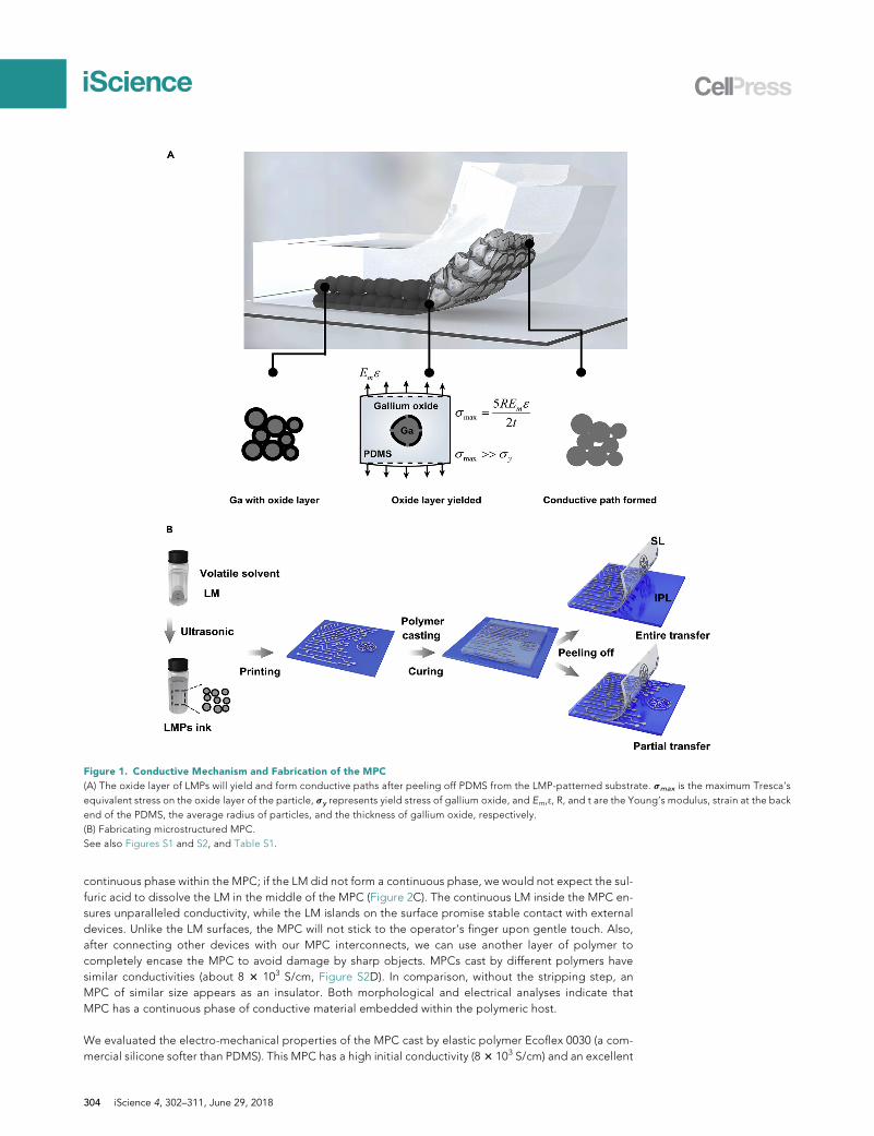
Figure 1. Conductive Mechanism and Fabrication of the MPC
(A) The oxide layer of LMPs will yield and form conductive paths after peeling off PDMS from the LMP-patterned substrate. smax is the maximum Tresca’s
equivalent stress on the oxide layer of the particle, sy represents yield stress of gallium oxide, and Em, 3, R, and t are the Young’s modulus, strain at the back
end of the PDMS, the average radius of particles, and the thickness of gallium oxide, respectively.
(B) Fabricating microstructured MPC.
See also Figures S1 and S2, and Table S1.
continuous phase within the MPC; if the LM did not form a continuous phase, we would not expect the sul-
furic acid to dissolve the LM in the middle of the MPC (Figure 2C). The continuous LM inside the MPC en-
sures unparalleled conductivity, while the LM islands on the surface promise stable contact with external
devices. Unlike the LM surfaces, the MPC will not stick to the operator’s finger upon gentle touch. Also,
after connecting other devices with our MPC interconnects, we can use another layer of polymer to
completely encase the MPC to avoid damage by sharp objects. MPCs cast by different polymers have
similar conductivities (about 8 3 103 S/cm, Figure S2D). In comparison, without the stripping step, an
MPC of similar size appears as an insulator. Both morphological and electrical analyses indicate that
MPC has a continuous phase of conductive material embedded within the polymeric host.
We evaluated the electro-mechanical properties of the MPC cast by elastic polymer Ecoflex 0030 (a com-
mercial silicone softer than PDMS). This MPC has a high initial conductivity (8 3 103 S/cm) and an excellent
304 iScience 4, 302–311, June 29, 2018
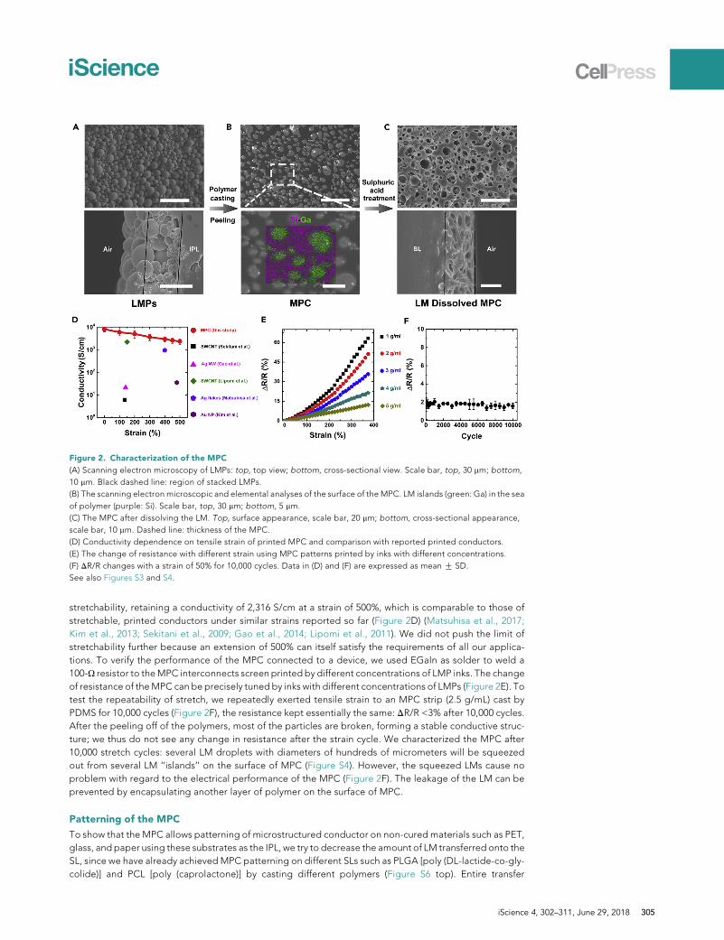
Figure 2. Characterization of the MPC
(A) Scanning electron microscopy of LMPs: top, top view; bottom, cross-sectional view. Scale bar, top, 30 mm; bottom,
10 mm. Black dashed line: region of stacked LMPs.
(B) The scanning electron microscopic and elemental analyses of the surface of the MPC. LM islands (green: Ga) in the sea
of polymer (purple: Si). Scale bar, top, 30 mm; bottom, 5 mm.
(C) The MPC after dissolving the LM. Top, surface appearance, scale bar, 20 mm; bottom, cross-sectional appearance,
scale bar, 10 mm. Dashed line: thickness of the MPC.
(D) Conductivity dependence on tensile strain of printed MPC and comparison with reported printed conductors.
(E) The change of resistance with different strain using MPC patterns printed by inks with different concentrations.
(F) DR/R changes with a strain of 50% for 10,000 cycles. Data in (D) and (F) are expressed as mean G SD.
See also Figures S3 and S4.
stretchability, retaining a conductivity of 2,316 S/cm at a strain of 500%, which is comparable to those of
stretchable, printed conductors under similar strains reported so far (Figure 2D) (Matsuhisa et al., 2017;
Kim et al., 2013; Sekitani et al., 2009; Gao et al., 2014; Lipomi et al., 2011). We did not push the limit of
stretchability further because an extension of 500% can itself satisfy the requirements of all our applica-
tions. To verify the performance of the MPC connected to a device, we used EGaIn as solder to weld a
100-U resistor to theMPC interconnects screen printed by different concentrations of LMP inks. The change
of resistance of theMPC can be precisely tuned by inks with different concentrations of LMPs (Figure 2E). To
test the repeatability of stretch, we repeatedly exerted tensile strain to an MPC strip (2.5 g/mL) cast by
PDMS for 10,000 cycles (Figure 2F), the resistance kept essentially the same: DR/R <3% after 10,000 cycles.
After the peeling off of the polymers, most of the particles are broken, forming a stable conductive struc-
ture; we thus do not see any change in resistance after the strain cycle. We characterized the MPC after
10,000 stretch cycles: several LM droplets with diameters of hundreds of micrometers will be squeezed
out from several LM ‘‘islands’’ on the surface of MPC (Figure S4). However, the squeezed LMs cause no
problem with regard to the electrical performance of the MPC (Figure 2F). The leakage of the LM can be
prevented by encapsulating another layer of polymer on the surface of MPC.
Patterning of the MPC
To show that the MPC allows patterning of microstructured conductor on non-cured materials such as PET,
glass, and paper using these substrates as the IPL, we try to decrease the amount of LM transferred onto the
SL, since we have already achieved MPC patterning on different SLs such as PLGA [poly (DL-lactide-co-gly-
colide)] and PCL [poly (caprolactone)] by casting different polymers (Figure S6 top). Entire transfer
iScience 4, 302–311, June 29, 2018 305
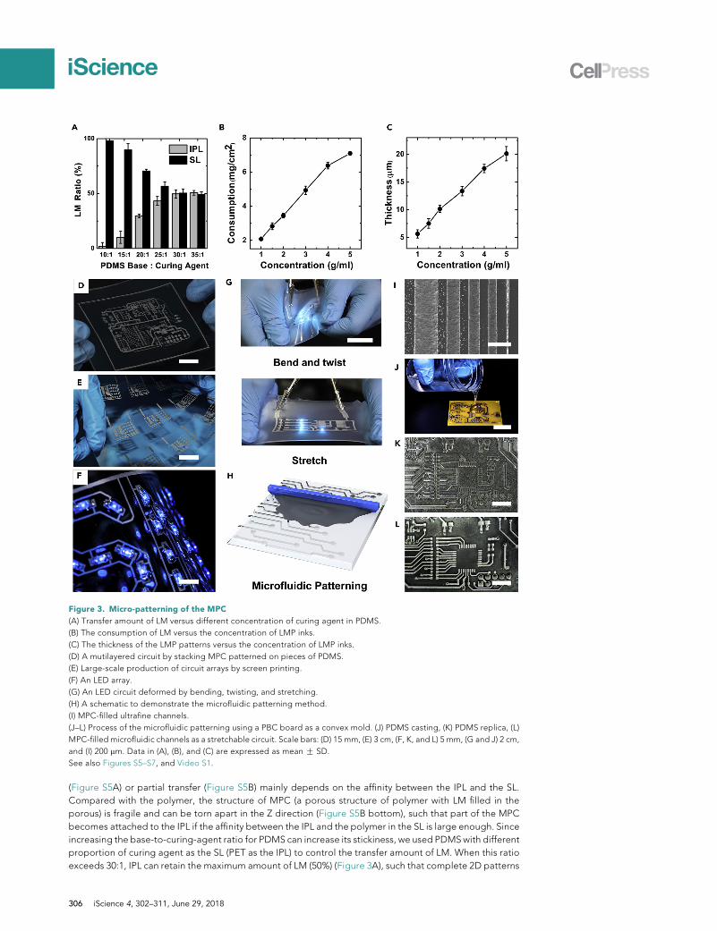
Figure 3. Micro-patterning of the MPC
(A) Transfer amount of LM versus different concentration of curing agent in PDMS.
(B) The consumption of LM versus the concentration of LMP inks.
(C) The thickness of the LMP patterns versus the concentration of LMP inks.
(D) A mutilayered circuit by stacking MPC patterned on pieces of PDMS.
(E) Large-scale production of circuit arrays by screen printing.
(F) An LED array.
(G) An LED circuit deformed by bending, twisting, and stretching.
(H) A schematic to demonstrate the microfluidic patterning method.
(I) MPC-filled ultrafine channels.
(J–L) Process of the microfluidic patterning using a PBC board as a convex mold. (J) PDMS casting, (K) PDMS replica, (L)
MPC-filled microfluidic channels as a stretchable circuit. Scale bars: (D) 15 mm, (E) 3 cm, (F, K, and L) 5 mm, (G and J) 2 cm,
and (I) 200 mm. Data in (A), (B), and (C) are expressed as mean G SD.
See also Figures S5–S7, and Video S1.
(Figure S5A) or partial transfer (Figure S5B) mainly depends on the affinity between the IPL and the SL.
Compared with the polymer, the structure of MPC (a porous structure of polymer with LM filled in the
porous) is fragile and can be torn apart in the Z direction (Figure S5B bottom), such that part of the MPC
becomes attached to the IPL if the affinity between the IPL and the polymer in the SL is large enough. Since
increasing the base-to-curing-agent ratio for PDMS can increase its stickiness, we used PDMSwith different
proportion of curing agent as the SL (PET as the IPL) to control the transfer amount of LM. When this ratio
exceeds 30:1, IPL can retain the maximum amount of LM (50%) (Figure 3A), such that complete 2D patterns
306 iScience 4, 302–311, June 29, 2018
formed on both IPL and SL. To keep the feature resolution intact on SL, we need to decrease the affinity
between the IPL and SL. To keep the feature resolution intact on IPL, we need to increase such affinity.
The surface in partial transfer reflects the inner structure of the MPC, which presents a continuous metallic
phase (Figure S3B). This strategy allows further broadening of the types of substrates on which we can
pattern flexible microstructured conductors. For instance, when using non-curable materials (Figure S6
bottom) as the IPL, they can keep the MPC patterns by using sticky PDMS as the SL. Some of these sub-
strates have features such as flexibility, biocompatibility, and biodegradability.
To test whether alloys other than EGaIn can be fabricated to MPC, we used LM with higher melting point.
We sonicated an alloy that melts at 47�C (Sn 8.30, Pb 22.60, Bi 44.70, Cd 5.30, In 19.10) into LMPs and utilize
partial transfer to fabricate the MPC on PET. At room temperature, the LM within the MPC is in solid state.
The MPC possesses excellent flexibility; after bending for 1,000 cycles, the conductivity remains the same
(Figure S7A). MPC can thus be a general approach for making flexible conductors by combining LM with a
variety of polymers, as long as the melting pointing of the metal alloy is within the working range of
polymers.
We can pattern the MPC into any complex 2D geometry using handwriting (Figure S7B), screen printing, or
microfluidic patterning (Figure 3H). To achieve rapid fabrication of patterns, we used screen printing to
make a batch of nine integrated circuits, each circuit controlling an array of light-emitting diode (LED) (Fig-
ure 3E). Each circuit is highly supple and can undergo repeated bending, twisting, and stretching without
compromising the function of any of its components (Figure 3G and Video S1). We achieved such circuit
array within 10 s, which suggested that an estimated number of 2,000 circuits can be obtained within 1
hour when taking the casting and peeling off process into account. Comparing with direct ink-jet printing
of LM, which requires LM 60 mg/cm2 (the patterns are usually 100 mm in thickness) (Wang et al., 2015), the
MPC fabricated by screen printing is unprecedented in minimizing the amount of metal, only several milli-
grams per square centimeter (depending on the concentration of inks, Figure 3B). The LMPs on the mesh
can be easily washed by ethanol. After the printing, we usually wash the mesh using ethanol and collect
such washed LMPs. After centrifugation, LMPs can be recycled. The thickness of the MPC can be controlled
by the concentration of the LMP inks (Figure 3C). We achieved MPC patterns on an ultrathin membrane
(30 mm) (Figure S7D). We successfully achieved multi-layered circuits by stacking MPC patterned on
pieces of PDMS (Figure 3D). This approach may allow us to ultimately make stretchable displays (Figures
3F and S7C).
We usedmicrofluidic patterningmethod to obtain ultra-fine interconnects. Briefly, we used a blade to scrap
the LMP inks into the microfluidic channels (Figure 3H). When scraping the LMP ink, the LMPs will not be
broken by blades because they are in a solution form (dispersed in solvent and cannot be sintered). After
evaporation of the solvents, we used sticky PDMS as the SL to retain half of theMPC in themicrofluidic chan-
nels. We achieved a minimum trace width of 15 mm on PDMS (Figure 3I) using this method (the discrete ink
residues by the wide lines caused by the surface tension of the solvents may be improved by increasing the
concentration of the LMP inks or by adding some surfactants). Microfluidic patterning method is also suit-
able for converting a Printed circuit board (PCB) into flexible and stretchable circuit. Using a PCB as a
convex mold (Figure 3J), we can replicate a concave microfluidic network, which allows the filling of LMP
inks (Figures 3K and 3L). Our MPC patterning strategies perfectly meet the requirements of the industrial
standard PCB, where the minimum trace width is �70 mm. Compared with conventional patterning strate-
gies of LM, the patterning of the MPC could be much more flexible, economic, and extremely high in yield.
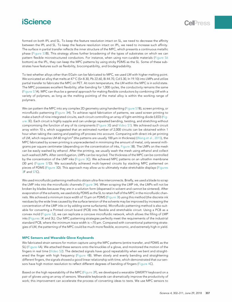
MPC Sensors and Wearable Glove Keyboards
We fabricated strain sensors for motion capture using the MPC patterns (entire transfer, and PDMS as the
SL) (Figure 4A). We attached these sensors onto the knuckles of a glove, and monitored the motion of the
fingers in real time (Video S2). The detected signals have good repeatability when we bent and straight-
ened the finger with high frequency (Figure 4B). When slowly and evenly bending and straightening
different fingers, the signals showed a good linear relationship with time, which demonstrated that our sen-
sors have high motion resolution to reflect different degrees of bending of fingers (Figure 4C).
Based on the high repeatability of the MPC (Figure 2F), we developed a wearable QWERTY keyboard on a
pair of gloves using an array of sensors. Wearable keyboards can dramatically improve the productivity of
work; this improvement can accelerate the process of converting ideas to texts. We use MPC sensors to
iScience 4, 302–311, June 29, 2018 307
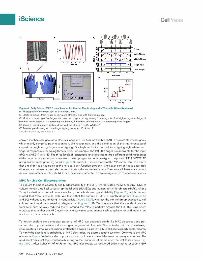
Figure 4. Fully Printed MPC Strain Sensors for Motion Monitoring and a Wearable Glove Keyboard
(A) Photograph of the strain sensor. Scale bar, 2 mm.
(B) Electrical signals from finger bending and straightening with high frequency.
(C) Motion monitoring of five fingers with slow bending and straightening: 1. making a fist; 2. straightening index finger; 3.
bending index finger; 4. straightening two fingers; 5. bending two fingers; 6. straightening three fingers.
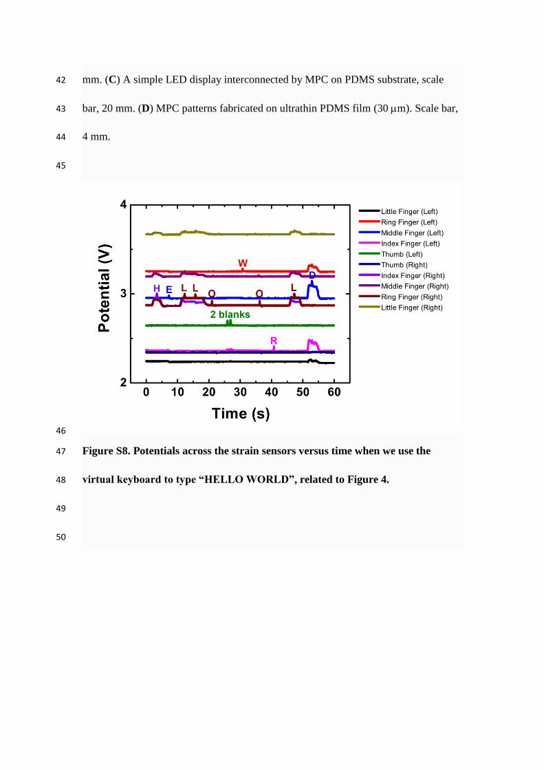
(D) Using a wearable glove keyboard to input the phrase ‘‘HELLO WORLD.’’
(E) An example showing left little finger typing the letters Q, A, and Z.
See also Figure S8, and Video S2.
convert mechanical signals into electrical ones and use Arduino and MATLAB to process electrical signals,
which mainly comprise peak recognition, cliff recognition, and the elimination of the interference peak
caused by neighboring fingers when typing. Our keyboard suits the traditional typing style where each
finger is responsible for typing three letters. For example, the left little finger is responsible for the input
of Q, A, and Z (Figure 4E). The three levels of resistance signals represent three different bending degrees
of the finger, whereas the peaks represent the tappingmovements. We typed the phrase ‘‘HELLOWORLD’’
using this wearable glove keyboard (Figures 4D and S8). The robustness of the MPC under stretch ensures
that a real device as complex as the keyboard can function properly. Since each sensor has to accurately
differentiate between at least six modes of stretch, the entire device with 10 sensors will have to accommo-
date 60 parameters repetitively. MPC can thus be instrumental in developing a series of wearable devices.
MPC for Live-Cell Electroporation
To explore the biocompatibility and biodegradability of the MPC, we fabricated the MPC cast by PDMS to
culture human umbilical vascular epithelial cells (HUVECs) and human aortic fibroblasts (HAFs). After a
7-day incubation in the cell culture medium, the cells showed good viability (Figure S9), which demon-
strated that MPC is safe to cells. We found that the surface of MPC is slightly degraded (Figures 5B
and 5C) without compromising its conductivity (Figure S10A), whereas the control group exposed to cell
culture medium alone showed no degradation (Figure S10B). We speculate that the metabolic wastes
from cells, such as CO2, reduced the pH around the MPC to partially dissolve the LM. This experiment
indicates that neither the MPC itself nor its dissolvable components (such as gallium ion and indium ion)
are toxic to mammalian cells.
To further explore the biomedical potential of MPC, we designed comb-like MPC electrodes and per-
formed electroporation to introduce exogenous genes into live cells. The controlled introduction of exog-
enous materials into live cells using stretchable devices is a potentially useful, but a poorly explored area.
To verify the excellent stretchability of MPC electrodes, we exerted tensile cycle for 100 times to the MPC
electrode (Figure 5A) before electroporation, using gold electrodes of the same geometry as a control. The
gold electrodes lost their conductivity owing to the formation of cracks after the first tensile cycle (Fig-
ure S10C). After adhesion of HAFs on the MPC electrodes, we delivered DNA plasmid encoding GFP
308 iScience 4, 302–311, June 29, 2018
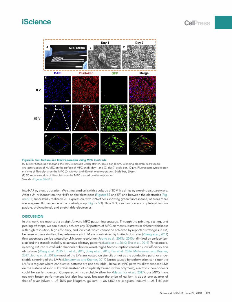
Figure 5. Cell Culture and Electroporation Using MPC Electrode
(A–E) (A) Photograph showing the MPC electrode under stretch, scale bar, 8 mm. Scanning electron microscopic
characterization of HUVEC on the surface of MPC on (B) day 1 and (C) day 7, scale bar, 10 mm. Fluorescent cytoskeleton
staining of fibroblasts on the MPC (D) without and (E) with electroporation. Scale bar, 50 mm.
(F) 3D reconstruction of fibroblasts on the MPC treated by electroporation.
See also Figures S9–S11.
into HAF by electroporation.We stimulated cells with a voltage of 80 V five times by exerting a square wave.
After a 24-hr incubation, the HAFs on the electrodes (Figures 5E and 5F) and between the electrodes (Fig-
ure S11) successfully realized GFP expression, with 95% of cells showing green fluorescence, whereas there
was no green fluorescence in the control group (Figure 5D). Thus MPC can function as completely biocom-
patible, biofunctional, and stretchable electronics.
DISCUSSION
In this work, we reported a straightforward MPC patterning strategy. Through the printing, casting, and
peeling off steps, we could easily achieve any 2D pattern of MPC on most substrates in different thickness
with high resolution, high efficiency, and low cost, which cannot be achieved by reported strategies in LM,
because in these studies, the performances of LM are constrained by limited substrates (Zheng et al., 2014)
(few substrates can be wetted by LM), poor resolution (Jeong et al., 2015a, 2015b) (limited by surface ten-
sion and the stencil), inability to achieve arbitrary patterns (Kubo et al., 2010; Zhu et al., 2013) (for example,
injecting LM into microfluidic channels or hollow wires), high LM consumption caused by low efficiency and
utilizations (Wang et al., 2015; Lin et al., 2015; Boley et al., 2015; Ren et al., 2016; Mohammed and Kramer,
2017; Jeong et al., 2015b) (most of the LMs are wasted on stencils or not as the conductive part), or unde-
sirable sintering of the LMPs (Mohammed and Kramer, 2017) (stress caused by deformation can sinter the
LMPs in regions where conductive patterns are not desirable). Because MPC patterns allow exposed LMs
on the surface of solid substrates (instead of completely buried within polymers), electronic components
could be easily mounted. Compared with stretchable silver ink (Matsuhisa et al., 2017), our MPCs have
not only better performances but also low cost, because the price of gallium is about one-quarter of
that of silver (silver: � US $530 per kilogram, gallium: � US $150 per kilogram, indium: � US $180 per
iScience 4, 302–311, June 29, 2018 309
kilogram, 2018) (as conductors, gallium and indium in high purity are not necessary), not to mention the
expensive processing of the microstructured silver. Our MPC patterning method meets the minimum trace
width requirements of the commercial PCB, and its low cost and high yields will make broad applications of
the LM-based electronic devices possible.
We can combine the benefits of both metals and polymers. We may use functional polymers such as shape
memory polymers, self-healing polymers, and biodegradable polymers to cast the LMPs to form thousands
of new functional MPCs in desirable temperature.
Our MPC also paves a brand new avenue for the implantable electronic devices. Based on the excellent
stretchability and biocompatibility of our MPC, stretchable patches can be designed for highly active or-
gans, such as the heart and joints. For example, in a myocardial infarction model, we intend to fabricate
a biodegradable cardiac patch patterned by MPC electrodes to enhance the conductivity of myocardial
cells and monitor the electrophysiological signals simultaneously.
The ease of fabrication and high level of biocompatibility will make MPC useful for wearable electronics,
implantable devices, soft robotics, future fabrics, virtual/augmented reality, flexible display, artificial
organs, brain-computer interface, and wherever biocompatible, soft electronics is necessary.
METHODS
All methods can be found in the accompanying Transparent Methods supplemental file.
SUPPLEMENTAL INFORMATION
Supplemental Information includes Transparent Methods, 11 figures, 1 table, and 2 videos and can be
found with this article online at https://doi.org/10.1016/j.isci.2018.05.013.
ACKNOWLEDGMENTS
We thank Zewen Wei and Deyao Zhao for their great help in electroporation. We thank the Ministry of Sci-
ence and Technology of China (2013YQ190467), Chinese Academy of Sciences (XDA09030305), and the
National Natural Science Foundation of China (81361140345, 51373043, and 21535001) for financial
support.
AUTHOR CONTRIBUTIONS
X.J. conceived and supervised this project. L.T. designed, fabricated, and characterized materials and de-
vices with the help of L.M., and S.Y., L.T., S.C., and Z.H. carried out cell experiments. L.Z. and X.S. per-
formed the calculation and simulation of the MPC. H.M. coded the virtual keyboard. L.T., S.C., and X.J.
wrote the manuscript. All authors discussed the results and commented on the manuscript.
DECLARATION OF INTERESTS
The authors declare that they have no competing interests.
Received: March 27, 2018
Revised: April 30, 2018
Accepted: May 1, 2018
Published: June 14, 2018
REFERENCES
Boley, J.W., White, E.L., and Kramer, R.K. (2015).Mechanically sintered gallium-indiumnanoparticles. Adv. Mater. 27, 2355–2360.Chortos, A., Liu, J., and Bao, Z. (2016). Pursuingprosthetic electronic skin. Nat. Mater. 15,937–950.
Dickey, M.D. (2014). Emerging applications ofliquid metals featuring surface oxides. ACS Appl.Mater. Interaces 6, 18369–18379.
310 iScience 4, 302–311, June 29, 2018
Dickey, M.D. (2017). Stretchable and softelectronics using liquid metals. Adv. Mater. 29.1606425. https://doi.org/10.1002/adma.201606425.
Gao, H.L., Xu, L., Long, F., Pan, Z., Du, Y.X., Lu, Y.,Ge, J., and Yu, S.H. (2014). Macroscopic free-standing hierarchical 3D architectures assembledfrom silver nanowires by ice templating. Angew.Chem. Int. Ed. 53, 4561–4566.
Jeong, J.W., McCall, J.G., Shin, G., Zhang, Y., Al-Hasani, R., Kim, M., Li, S., Sim, J.Y., Jang, K.I., Shi,Y., et al. (2015a). Wireless optofluidic systems forprogrammable in vivo pharmacology andoptogenetics. Cell 162, 662–674.
Jeong, S.H., Hjort, K., and Wu, Z. (2015b). Tapetransfer atomization patterning of liquid alloys formicrofluidic stretchable wireless power transfer.Sci. Rep. 5, 8419.
Kang, S., Murphy, R.K.J., Hwang, S., Lee, S.M.,Harburg, D.V., Krueger, N.A., Shin, J., Gamble, P.,Cheng, H., Yu, S., et al. (2016). Bioresorbablesilicon electronic sensors for the brain. Nature530, 71–76.
Kazem, N., Hellebrekers, T., and Majidi, C. (2017).Soft multifunctional composites and emulsionswith liquid metals. Adv. Mater. 29, 1–14.
Kim, D.H., Song, J., Choi, W.M., Kim, H.S., Kim,R.H., Liu, Z., Huang, Y.Y., Hwang, K.C., Zhang, Y.,and Rogers, J.A. (2008). Materials andnoncoplanar mesh designs for integrated circuitswith linear elastic responses to extrememechanical deformations. Proc. Natl. Acad. Sci.USA 105, 18675–18680.
Kim, D.H., Lu, N., Ma, R., Kim, Y.S., Kim, R.H.,Wang, S., Wu, J., Won, S.M., Tao, H., Islam, A.,et al. (2011). Epidermal electronics. Science 333,838–843.
Kim, Y., Zhu, J., Yeom, B., Di Prima, M., Su, X.,Kim, J.G., Yoo, S.J., Uher, C., and Kotov, N.A.(2013). Stretchable nanoparticle conductors withself-organized conductive pathways. Nature 500,59–63.
Kubo, M., Li, X., Kim, C., Hashimoto, M., Wiley,B.J., Ham, D., and Whitesides, G.M. (2010).Stretchable microfluidic radiofrequencyantennas. Adv. Mater. 22, 2749–2752.
Lin, Y., Cooper, C., Wang, M., Adams, J.J.,Genzer, J., and Dickey, M.D. (2015). Handwritten,soft circuit boards and antennas using liquidmetal nanoparticles. Small 11, 6397–6403.
Lipomi, D.J., Vosgueritchian, M., Tee, B.C.K.,Hellstrom, S.L., Lee, J.A., Fox, C.H., and Bao, Z.(2011). Skin-like pressure and strain sensors based
on transparent elastic films of carbon nanotubes.Nat. Nanotechnol. 6, 788–792.
Liu, J., Fu, T.M., Cheng, Z., Hong, G., Zhou, T., Jin,L., Duvvuri, M., Jiang, Z., Kruskal, P., Xie, C., et al.(2015). Syringe-injectable electronics. Nat.Nanotechnol. 10, 629–636.
Lou, Z., Chen, S., Wang, L., Shi, R., Li, L., Jiang, K.,Chen, D., and Shen, G. (2017). Ultrasensitive andultra flexible E-skins with dual functionalities forwearable electronics. Nano Energy 38, 28–35.
Lu, Y., Hu, Q., Lin, Y., Pacardo, D.B., Wang, C.,Sun, W., Ligler, F.S., Dickey, M.D., and Gu, Z.(2015). Transformable liquid-metalnanomedicine. Nat. Commun. 6, 10066.
Matsuhisa, N., Inoue, D., Zalar, P., Jin, H.,Matsuba, Y., Itoh, A., Yokota, T., Hashizume, D.,and Someya, T. (2017). Printable elasticconductors by in situ formation of silvernanoparticles from silver flakes. Nat. Mater. 5,1–8.
Mohammed, M.G., and Kramer, R. (2017). All-printed flexible and stretchable electronics. Adv.Mater. 29. 1604965. https://doi.org/10.1002/adma.201604965.
Oh, J.Y., Rondeau-gagne, S., Chiu, Y., Chortos,A., Lissel, F., Wang, G.N., Schroeder, B.C.,Kurosawa, T., Lopez, J., Katsumata, T., et al.(2016). Intrinsically stretchable and healablesemiconducting polymer for organic transistors.Nature 539, 411–415.
Qi, D., Liu, Z., Liu, Y., Leow, W.R., Zhu, B., Yang,H., Yu, J., Wang, W., Wang, H., Yin, S., et al.(2015). Suspended wavy graphene microribbonsfor highly stretchable microsupercapacitors. Adv.Mater. 27, 5559–5566.
Ren, L., Zhuang, J., Casillas, G., Feng, H., Liu, Y.,Xu, X., Liu, Y., Chen, J., Du, Y., Jiang, L., et al.(2016). Nanodroplets for stretchablesuperconducting circuits. Adv. Funct. Mater. 26,8111–8118.
Sekitani, T., Nakajima, H., Maeda, H.,Fukushima, T., Aida, T., Hata, K., and Someya,T. (2009). Stretchable active-matrix organiclight-emitting diode display usingprintable elastic conductors. Nat. Mater. 8,494–499.
Sun, J., Xianyu, Y., and Jiang, X. (2014). Point-of-care biochemical assays using gold Nanoparticle-implemented Microfluidics. Chem. Soc. Rev. 43,6239–6253.
Tang, Y., Gong, S., Chen, Y., Yap, L.W., andCheng, W. (2014). Manufacturable conductingrubber ambers and stretchable conductors fromcopper nanowire aerogel monoliths. ACS Nano.8, 5707–5714.
Wang, Q., Yu, Y., Yang, J., and Liu, J. (2015). Fastfabrication of flexible functional circuits based onliquid metal dual-trans printing. Adv. Mater. 27,7109–7116.
Zheng, Y., He, Z.Z., Yang, J., and Liu, J. (2014).Personal electronics printing via tapping modecomposite liquid metal ink delivery and adhesionmechanism. Sci. Rep. 4, 4588.
Zhu, S., So, J.H., Mays, R., Desai, S., Barnes, W.R.,Pourdeyhimi, B., and Dickey, M.D. (2013).Ultrastretchable fibers with metallic conductivityusing a liquid metal alloy core. Adv. Funct. Mater.23, 2308–2314.
iScience 4, 302–311, June 29, 2018 311

ISCI, Volume 4
Supplemental Information
Printable Metal-Polymer Conductors
for Highly Stretchable Bio-Devices
Lixue Tang, Shiyu Cheng, Luyao Zhang, Hanbing Mi, Lei Mou, Shuaijian Yang, ZhiweiHuang, Xinghua Shi, and Xingyu Jiang
SUPPLEMENTAL FIGURES 1
2
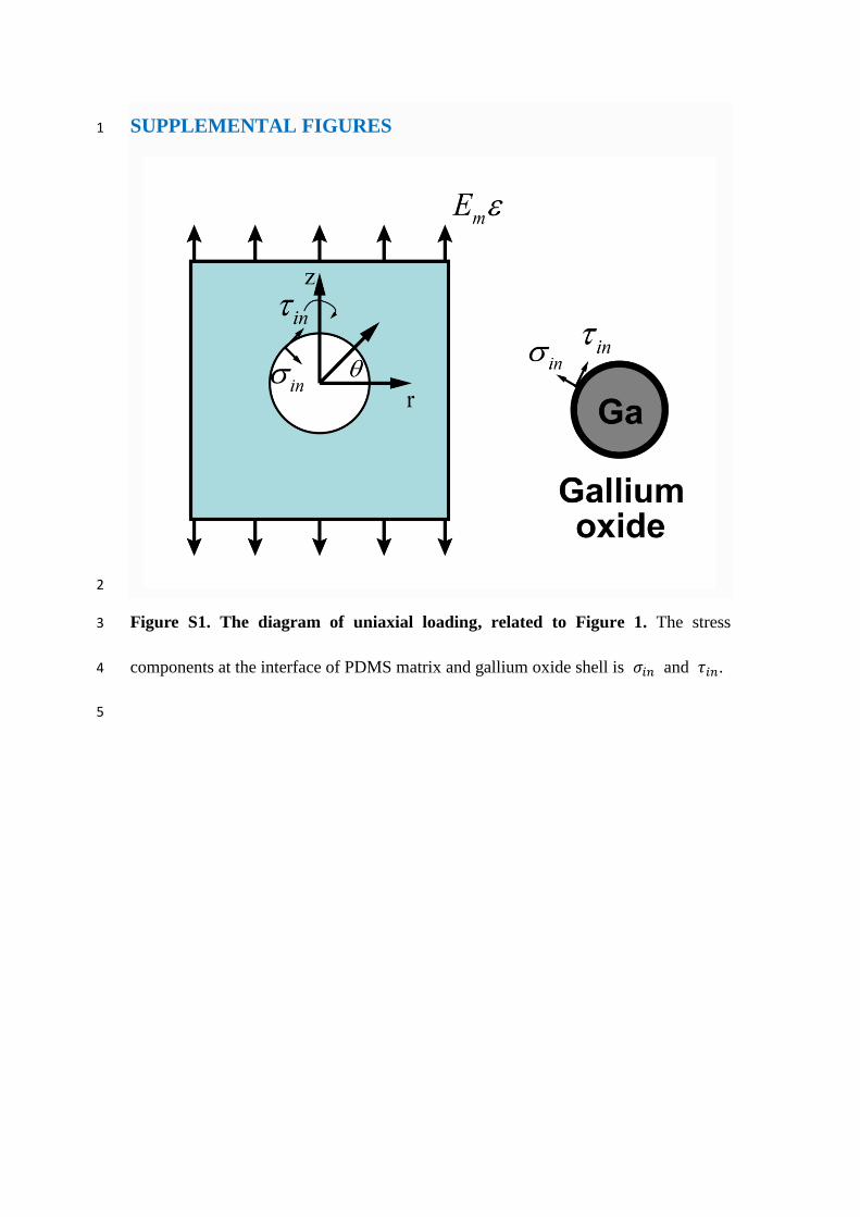
Figure S1. The diagram of uniaxial loading, related to Figure 1. The stress 3
components at the interface of PDMS matrix and gallium oxide shell is 𝜎𝑖𝑛 and 𝜏𝑖𝑛. 4
5
6
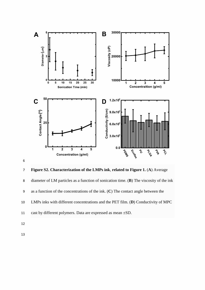
Figure S2. Characterization of the LMPs ink, related to Figure 1. (A) Average 7
diameter of LM particles as a function of sonication time. (B) The viscosity of the ink 8
as a function of the concentrations of the ink. (C) The contact angle between the 9
LMPs inks with different concentrations and the PET film. (D) Conductivity of MPC 10
cast by different polymers. Data are expressed as mean ±SD. 11
12
13
14
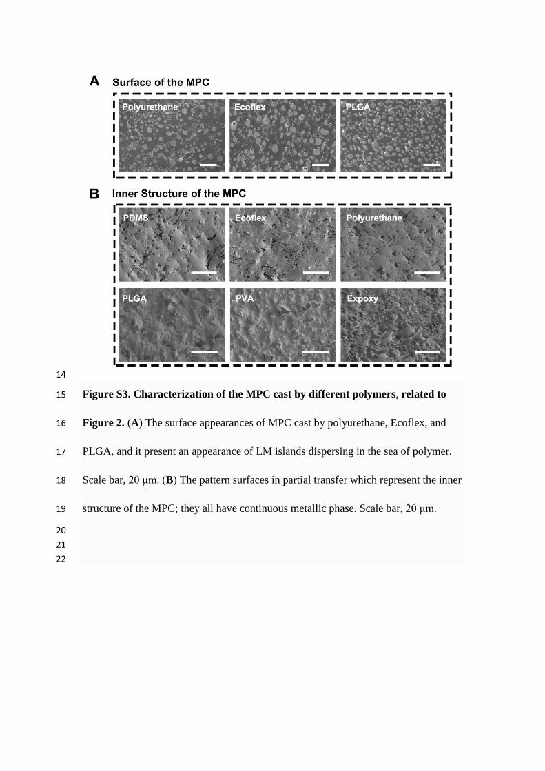
Figure S3. Characterization of the MPC cast by different polymers, related to 15
Figure 2. (A) The surface appearances of MPC cast by polyurethane, Ecoflex, and 16
PLGA, and it present an appearance of LM islands dispersing in the sea of polymer. 17
Scale bar, 20 μm. (B) The pattern surfaces in partial transfer which represent the inner 18
structure of the MPC; they all have continuous metallic phase. Scale bar, 20 μm. 19
20
21
22
23
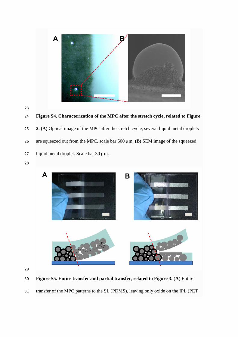
Figure S4. Characterization of the MPC after the stretch cycle, related to Figure 24
2. (A) Optical image of the MPC after the stretch cycle, several liquid metal droplets 25
are squeezed out from the MPC, scale bar 500 m. (B) SEM image of the squeezed 26
liquid metal droplet. Scale bar 30 m. 27
28
29
Figure S5. Entire transfer and partial transfer, related to Figure 3. (A) Entire 30
transfer of the MPC patterns to the SL (PDMS), leaving only oxide on the IPL (PET 31
film). (B) Partial transfer of the MPC patterns, and both of the IPL and SL have 32
integrated MPC pattern. Scale bar 10 mm. 33
34
Figure S6. MPC transfer to different substrates, related to Figure 3. Scale bar, 10 35
mm. 36
37
38
Figure S7. MPC patterns as interconnects, related to Figure 3. (A) Conductivity 39
changes with the bending for 1,000 cycles. (B) We use handwriting method to 40
fabricate a flexible and stretchable LED circuit on the PDMS substrate. Scale bar, 15 41
mm. (C) A simple LED display interconnected by MPC on PDMS substrate, scale 42
bar, 20 mm. (D) MPC patterns fabricated on ultrathin PDMS film (30 m). Scale bar, 43
4 mm. 44
45
46
Figure S8. Potentials across the strain sensors versus time when we use the 47
virtual keyboard to type “HELLO WORLD”, related to Figure 4. 48
49
50
51
Figure S9. Viability test of the HUVECs on the MPC-PDMS interface after 7 52
days, related to Figure 5. Cells are stained by Calcein-AM green (Invitrogen, US), 53
Scale bar, (top) 400 m, (bottom) 100 m. 54
55
56
Figure S10. Tolerance of the MPC and the gold electrode, related to Figure 5. (A, 57
B) Degradation exploration of the MPC. (A) Conductivity of the MPC dependence on 58
culturing time. (B) SEM characterization of the surface of MPC electrodes exposed in 59
DMEM. Scale bar, 10 m. (C) The gold electrode on the PDMS substrates lost its 60
conductivity after the tensile cycle due to the forming of cracks. Scale bar, 500 m. 61
Data are expressed as mean ±SD 62
63
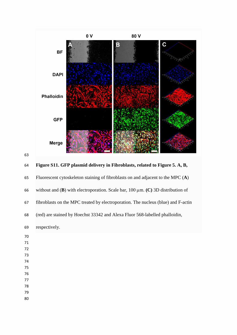
Figure S11. GFP plasmid delivery in Fibroblasts, related to Figure 5. A, B, 64
Fluorescent cytoskeleton staining of fibroblasts on and adjacent to the MPC (A) 65
without and (B) with electroporation. Scale bar, 100 m. (C) 3D distribution of 66
fibroblasts on the MPC treated by electroporation. The nucleus (blue) and F-actin 67
(red) are stained by Hoechst 33342 and Alexa Fluor 568-labelled phalloidin, 68
respectively. 69
70
71
72
73
74
75
76
77
78
79
80
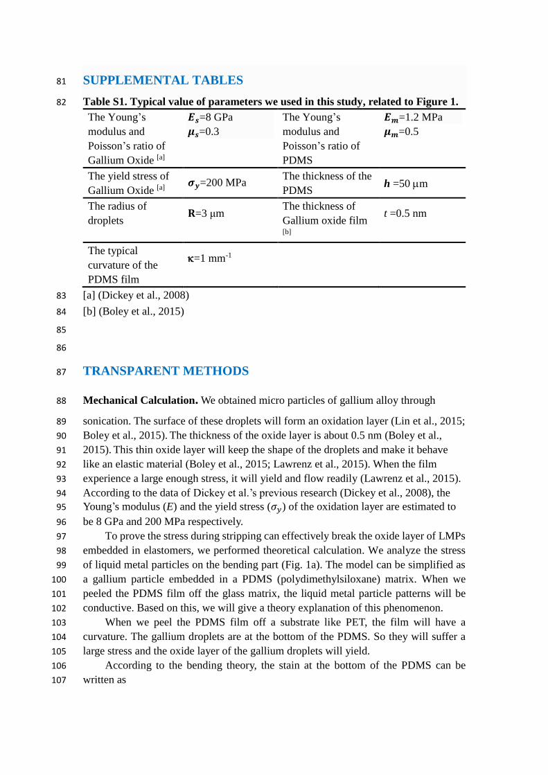
SUPPLEMENTAL TABLES 81
Table S1. Typical value of parameters we used in this study, related to Figure 1. 82
The Young’s
modulus and
Poisson’s ratio of
Gallium Oxide [a]
𝑬𝒔=8 GPa
𝝁𝒔=0.3
The Young’s
modulus and
Poisson’s ratio of
PDMS
𝑬𝒎=1.2 MPa
𝝁𝒎=0.5
The yield stress of
Gallium Oxide [a] 𝝈𝒚=200 MPa
The thickness of the
PDMS h =50 m
The radius of
droplets 𝐑=3 μm
The thickness of
Gallium oxide film [b]
t =0.5 nm
The typical
curvature of the
PDMS film
=1 mm-1
[a] (Dickey et al., 2008) 83
[b] (Boley et al., 2015) 84
85
86
TRANSPARENT METHODS 87
Mechanical Calculation. We obtained micro particles of gallium alloy through 88
sonication. The surface of these droplets will form an oxidation layer (Lin et al., 2015; 89
Boley et al., 2015). The thickness of the oxide layer is about 0.5 nm (Boley et al., 90
2015). This thin oxide layer will keep the shape of the droplets and make it behave 91
like an elastic material (Boley et al., 2015; Lawrenz et al., 2015). When the film 92
experience a large enough stress, it will yield and flow readily (Lawrenz et al., 2015). 93
According to the data of Dickey et al.’s previous research (Dickey et al., 2008), the 94
Young’s modulus (E) and the yield stress (𝜎𝑦) of the oxidation layer are estimated to 95
be 8 GPa and 200 MPa respectively. 96
To prove the stress during stripping can effectively break the oxide layer of LMPs 97
embedded in elastomers, we performed theoretical calculation. We analyze the stress 98
of liquid metal particles on the bending part (Fig. 1a). The model can be simplified as 99
a gallium particle embedded in a PDMS (polydimethylsiloxane) matrix. When we 100
peeled the PDMS film off the glass matrix, the liquid metal particle patterns will be 101
conductive. Based on this, we will give a theory explanation of this phenomenon. 102
When we peel the PDMS film off a substrate like PET, the film will have a 103
curvature. The gallium droplets are at the bottom of the PDMS. So they will suffer a 104
large stress and the oxide layer of the gallium droplets will yield. 105
According to the bending theory, the stain at the bottom of the PDMS can be 106
written as 107
=2
h (1) 108
In which, h is the thickness of the PDMS and κ is the curvature radius of the PDMS. 109
We will calculate the relation of the stress of gallium droplet and the PDMS strain ε. As 110
shown in fig. S1, the PDMS matrix is assumed as an infinite solid and the gallium 111
droplet with a thin oxide layer is assumed as a thin walled sphere with a radius R and a 112
thickness t. Far from the sphere, the matrix is subjected to a tensile stress 𝜎𝑧 = 𝐸𝑚𝜀, 113
with all other stress componets zero. The stress field of PDMS matrix 𝜎𝑖𝑗′ is 114
3 5 3 5
3 1 19 3 cos2
2 2 2 2r
B D C DA C B
r r r r
(2) 115
3 5 5
7cos2
2 2 8 2 8
B A D B D
r r r
(3) 116
3 5 5
3 5cos2
2 8 8
A D D
r r r (4) 117
3 5
3sin2
2 2r
B C D
r r
(5) 118
And in which, A, B, C, D are constants which are determined by the boundary 119
conditions. Then the stress filed of the oxide layer of the gallium droplet 𝜎𝑖𝑗 can be 120
written as 121
= cos2R
H It
(6) 122
cos2a b
RH I
t (7) 123
Where H, I and 𝜎𝑏 are constants. And the boundary condition is at 𝑟 → ∞, 124
cos22 2
m mr
E E , sin2
2
mr
E
(8) 125
And finally, we can obtain the maximum Tresca’s equivalent stress of the oxide layer 126
is 127
max
5
2
mRE
t
(9) 128
The typical value of parameters we used in this study are listed in table S1. Substituting 129
the value in table 1 in the Equation (9), we obtain 130
max 4500 MPa 131
And this value is great larger than the yield stress of gallium oxide (about 200 MPa). 132
So the oxide layer of the gallium droplet will yield. 133
134
Preparation of the low-melting metal particle inks. 1 g, 1.5 g, 2g, 2.5 g, 3 g, 4 g, and 135
5 g EGaIn (Gallium Indium eutectic, 99.99%, Sigma-Aldrich) was added into 5 mL 136
centrifuge tube filled with 1 mL n-Decyl alcohol (98%, MACKLIN, China), 137
respectively and sonicated by a sonicator (Scientz, Scientz-IID). For screen printing, 138
we sonicated the EGaIn for 1 min with the power of 300 W. For microfluidic patterning, 139
5 min with 300 W is required. 140
We also adopted alloy with melting point 47 oC (Sn 8.30, Pb 22.60, Bi 44.70, Cd 141
5.30, In 19.10, Taobao, China) to prepare the low-melting metal particle inks. 2.5 g 142
alloy was added to 1 mL n-Decyl alcohol (98%, MACKLIN, China). We heated the 143
alloy in an oven at 80 oC for 10 min to melt the alloy and sonicated the melting alloy 144
for 1 min with the power of 300 W. 145
146
Screen printing of the LMPs ink. The printing of liquid metal particle was realized 147
by a screen printing equipment (Taobao, China). We used the liquid metal particle ink 148
to print desired patterns on various substrates including PET, PCL, PLGA, PDMS 149
films, A4 paper, and glass with 200 mesh screen printing plates. 150
151
Microfluidic patterning of the LMPs ink. The microstructures are obtain by soft 152
lithography. Briefly, we used silicon wafer or printed circuit boards (PCB) as the 153
master molds. To obtain silicon wafer as the master wafer, we followed standard 154
photolithography. Master fabrication for the microfluidic channels begins with spin 155
coating negative photoresists (SU8 2035, MicroChem Corp., US) on a silicon wafer at 156
1200 rpm for 30 s (100 μm thick). After baking the photoresist at 95 oC for 5 min, the 157
wafer was exposed to UV light for 90 s through a mask. After baking the wafer at 95 158 oC for 10 min, we immersed the wafer into a developer (SU8 developer, MicroChem 159
Corp, US.) and washed it for 5 min. 160
We also use the PCB (Jiekecengfeng Corp., China) as the master wafer. The 161
thickness of the copper film is 150 μm. We cast a layer of PDMS onto the master 162
mold. After baking in an oven at 80 oC for 40 min, we removed the PDMS replica 163
from master. We spread LM particle inks onto the patterned PDMS. Before the 164
evaporation of the solvent, we filled the microfluidic channel with EGaIn particle ink 165
using a blade or squeegee, and excess ink was scraped off the substrate. 166
167
The fabrication of MPC by casting and peeling. After evaporation of the solvent, 168
we used various polymers for casting on the patterned LMPs. We dissolved poly 169
(carprolactone) (PCL, Mn=80000 g/mol, Sigma-Aldrich, US) pellets in 170
dimethylformamide (DMF, ThermoFisher Scientific, US) and CH2Cl2 (Aladdin, 171
China) with a ratio of 1:3 (w/w) at 5 wt% to prepare the PCL solution. We prepared 172
the 5 wt% poly (vinyl alcohol) (PVA) (1795, Aladdin, China) solution (w/w) by 173
dissolving PVA in ultrapure water (Milli-Q Reference, MERCK, France) in water bath 174
at 95 oC for 1 hour. We dissolved poly (DL-lactide-co-glycolide) (PLGA 75:25, 175
Mw=114 kDa, Lakeshore Biomaterials, US) particles in acetone/DMF with a ratio of 176
2:1 (w/w) at 5 wt% to prepare the PLGA solution. We prepared the PDMS prepolymer 177
by mixing base and curing agent with a ratio of 10:1, 15:1, 20:1, 25:1, 30:1, and 35:1 178
(w/w). We prepared the Ecoflex prepolymer by mixing part A and part B with a ratio 179
of 1:1 (w/w). We prepared the epoxy sealant prepolymer (epoxy sealant, Ausbond, 180
US) by mixing part A and part B with a ratio of 5:4 (w/w). We prepared the 181
polyurethane (PU) (polyurethane sealant, Ausbond, US) prepolymer by mixing part A 182
and part B with a ratio of 1:1 (w/w). These prepolymers were thoroughly mixed and 183
degassed in a mixer (AR-100, THINKY, Japan). 184
We cast polymer solutions or prepolymers onto the LMPs patterns. These cast 185
polymer solutions were placed in a chemical hood in room temperature for 24 h to 186
volatile solvents. While the cast PDMS, PU, and epoxy resin prepolymers were 187
placed in 80 oC oven for 40 min or in room temperature for 12 hours. 188
After curing, these polymer films were peeled off from the substrates. Thus 189
conductive MPC on different polymer substrates were obtained either on IPL or SL. 190
To obtain MPC patterns on the PDMS ultrathin film (30 m), we spin-coated the 191
PDMS at 4500 r for 20 s after the casting process. 192
193
Particles and MPC characterization. Inks (2.5 g/mL for 1 min) for Scanning 194
Electron Microscopy (SEM, S4800, Hitachi, Japan) characterizations were fabricated 195
by sonicating EGaIn for 1 min, 5 min, 10 min, 20 min, and 30 min, respectively. We 196
deposited 100 μL suspension on conductive tape via micropipette (Eppendorf, 197
Germany) and allowed them to dry in 80 oC oven for 10 min. MPC for SEM 198
characterizations were prepared by screen printing using different polymers as SL 199
(PDMS, Ecoflex, PLGA, PVA, PCL, PU, and epoxy resin). 200
The LM dissolved MPC for SEM characterizations were fabricated by 201
immersing the MPC patterns (2.5 g/mL) on 0.1 M sulfuric acid for 10 h. We use the 202
LM dissolved MPC for the thickness measurements. Briefly, we cut the sample with a 203
blade and characterized the cross section of the sample using SEM. 204
205
Measurement of the liquid metal consumptions and transfer amount of the MPC. 206
We used screen printing method to print liquid metal particles (2.5 g/mL) on PET 207
films as a shape of a strip (3*30 mm). After the evaporation of solution in an oven at 208
80 oC for 10 min, we cast PDMS of different ratio (10:1, 15:1, 20:1, 25:1, and 30:1) 209
on different PET films, respectively. The PDMS films were peeling from PET films 210
after curing in 80 oC for 40 min. We weighed these PET films using a precision 211
balance (AL104, METTLER TOLEDO, Swizerland) before printing, after printing, 212
after evaporation, and after peeling off, respectively. 213
214
Tensile test. Samples for stretching test were prepared by screen printing inks with 215
concentration of 1 g/ml, 2 g/ml, 3 g/ml, 4 g/ml, and 5 g/ml, respectively. We made the 216
MPC into a strip shape (800 μm in width and 4 cm in length) using PET as the IPL 217
and Ecoflex as the SL. The MPC strips were connected with a 100 Ω resistance and 218
mounted on a homemade frame. We measured resistance of the MPC using 219
multimeter (8846A, FLUKE, US) when they were gradually stretched to 500% strain. 220
221
Cycling test. Samples for stretching cycling test were prepared by screen printing 222
EGaIn inks with concentration of 2.5 g/ml. Samples for bending cycling test were 223
prepared by screen printing 47 oC low melting alloy particle inks with concentration 224
of 2.5 g/ml. We made the MPC into a strip shape (800 μm in width and 2 cm in 225
length) using PET as the IPL and PDMS (10:1) as the SL. We performed the 226
stretching cycling test for 10,000 cycles using a dynamic mechanic analysis (DMA 227
Q800, TA Instruments, US) under a strain rate of 100% /min with maximum strain of 228
50%. We performed the bending tests on dynamic mechanic analysis under a strain 229
rate of 100% /min with a displacement of 1 cm for 1,000 cycles 230
231
Circuits assembly. To assembly a functional circuits, we first used a pipette to add 2 232
μL EGaIn onto each contact pad of interconnects. Subsequently, we gently rubbed 233
EGaIn into the surface of electronic components to wet their pins and connected 234
electronic components with the touch pads. Finally, a layer of elastomer was cast to 235
encapsulate the circuits. 236
237
Fabrication and characterization of the strains sensors and virtual keyboard. We 238
printed EGaIn LMPs ink (2.5 g/mL) on PET films by screen printing as serpentine 239
shapes with the width of 200 m. After solvent evaporation at 80 oC for 10 min, we 240
spin-coated the PDMS (10:1) at 1000 r for 20 s on the LMPs patterns. . After curing at 241
80 oC for 30 min, the PDMS films with serpentine MPC (strain sensors) were 242
carefully peeled off from PET films. We used silica adhesive (3145 RTV, Dow 243
Corning, US) to attach strain sensors on a glove to monitor the motion of different 244
fingers by capturing resistance change. 245
We wore the strain sensors-mounted glove to monitor motions of fingers. The 246
strain sensors were connected to electrochemical workstation (1040C, CH 247
Instruments, US). We tested the resistant changes of the sensors by using the 248
technique amperometric i-t curve at potential 0.001 V. 249
The virtual keyboards were achieved by connecting the glove to Arduino 250
(MEGA 2560, ITALY), and processed signals using MATLAB. 251
252
Cell culture, staining and characterization. Samples for cell experiments were 253
prepared by screen printing inks with concentration of 2.5 g/ml. We made the MPC 254
using PET as the IPL and PDMS (10:1) as the SL. Before cell culture, we sterilized all 255
the samples by radiation with a cobalt radiation device (Co 5 60, 10-130 Gymin-1, 256
Peking University, China). The MPC was incubated with fibronectin solution (50 257
μg/ml) for 6 h at room temperature to promote the adhesion of cells. We seeded 258
human umbilical vein endothelial cells (HUVECs, ATCC, US) and human aortic 259
fibroblasts (Science Cell, US) on the surface of the MPC, and culture them in DMEM 260
supplemented with 10% fetal bovine serum (5% CO2, 37 oC) for 7 days. HUVECs 261
were stained with live/dead kit (Invitrogen, US) for cell viability test. Briefly, we 262
fixed cells with 4% paraformaldehyde aqueous solution for 10 min. Subsequently, we 263
stained the cells with the dyes at a concentration of 1 μg/mL for 20 min, and removed 264
excess dyes by 3 times rinsing the cells with phosphate buffered saline (PBS). 265
(Invitrogen, US) We stained the nucleus with Hoechst 33342 (Invitrogen, US) at a 266
concentration of 1 μL/mL for 5 min, and removed excess dyes by 3 times rinsing the 267
cells with PBS. We stained the F-actin with Alexa Fluor 568-labelled phalloidin 268
(Invitrogen, US) at a concentration of 200 units/mL for 20 min, and removed excess 269
dyes by 5 times rinsing the cells with PBS. The fluorescent images of cells was taken 270
by laser scanning confocal microscopy (LSM 710, Zeiss, Germany). Before SEM 271
characterization, we fixed cells with 4% paraformaldehyde aqueous solution for 30 272
min and dehydrated the sample with ethanol at the concentrations of 50%, 75%, and 273
100% for 10 min, sequentially. 274
275
Electroporation. We printed the MPC electrodes for electroporation with 2.5 g/mL 276
EGaIn LMPs, using PDMS (10:1) as the SL and PET as the IPL. We deposited 100 277
nm thick gold on the surface of PDMS by evaporation (Ohmiker-50B, Cello 278
Technology Corporation, Taiwan) to fabricate gold electrodes as a control group. 279
Human aortic fibroblasts were used to verify the electroporation of green fluorescent 280
protein (GFP, RiboBio, China). We incubated the MPC electrodes with the 281
fibronectin plasma solution (50 μg/ml) for 6 h at room temperature to promote 282
adhesion of cells. Subsequently, fibroblasts were delivered on the MPC electrode 283
(PDMS as the substrates) and cultured for 24 h. We washed the sample 3 times before 284
electroporation and immersed the surface of the electrodes in GFP solution at a 285
concentration of 40 μg/ml. We applied 5 electrical pulses using an electroporator by 286
exerting a square wave pulse (Electro Square Porator TM ECM 830, BTX, USA). The 287
voltage is 80 V, the pulse duration is 100 s, and the pulse interval is 1 s. After 288
culturing for 24 h, we stained the cells as above-mentioned and used confocal 289
microscopy to image the cells. 290
291
SUPPLEMENTAL REFERENCES 292
Lawrenz, F.; Lange, P.; Severin, N.; Rabe, J. P.; Helm, C. A.; Block, S. Morphology, Mechanical 293
Stability, and Protective Properties of Ultrathin Gallium Oxide Coatings. (2015). Langmuir 31, 294
5836–5842. 295
Dickey, B. M. D.; Chiechi, R. C.; Larsen, R. J.; Weiss, E. A.; Weitz, D. A.; Whitesides, G. M. 296
Eutectic Gallium-Indium (EGaIn): A Liquid Metal Alloy for the Formation of Stable Structures in 297
Microchannels at Room Temperature. (2008). Adv. Funct. Mater. 18, 1097-1104. 298
299
300