Embed Size (px)
Citation preview
Resonant tunnelling between the chiral Landau states oftwisted graphene lattices
M.T. Greenaway1, E.E. Vdovin1,2,3, A. Mishchenko4, O. Makarovsky1, A. Patane1, J.R. Wallbank5,
Y. Cao6, A.V. Kretinin6, M.J. Zhu4, S. V. Morozov2,3,
V.I. Fal’ko5, K.S. Novoselov4, A.K. Geim4,6, T.M. Fromhold1 and L. Eaves1,41School of Physics and Astronomy, University of Nottingham NG7 2RD UK
2Institute of Microelectronics Technology and High Purity Materials, RAS, Chernogolovka 142432, Russia3National University of Science and Technology ”MISiS”, 119049, Leninsky pr.4, Moscow, Russia
4School of Physics and Astronomy, University of Manchester, M13 9PL, UK5Physics Department, Lancaster University, Lancaster LA1 4YB, UK
6Centre for Mesoscience and Nanotechnology, University of Manchester, M13 9PL, UK(Dated: July 14, 2016)
Paper published on 19th October 2015: Nature Physics11, 10571062 (2015), doi:10.1038/nphys3507
A class of multilayered functional materials hasrecently emerged in which the component atomiclayers are held together by weak van der Waalsforces that preserve the structural integrity andphysical properties of each layer. An exemplar ofsuch a structure is a transistor device in whichrelativistic Dirac Fermions can resonantly tun-nel through a boron nitride barrier, a few atomiclayers thick, sandwiched between two grapheneelectrodes. An applied magnetic field quantisesgraphene’s gapless conduction and valence bandstates into discrete Landau levels, allowing us toresolve individual inter-Landau level transitionsand thereby demonstrate that the energy, mo-mentum and chiral properties of the electronsare conserved in the tunnelling process. We alsodemonstrate that the change in the semiclassi-cal cyclotron trajectories, following an inter-layertunnelling event, is analogous to the case of intra-layer Klein tunnelling.
An electron moving through the hexagonal crystalstructure of graphene is not only quasi-relativistic butalso exhibits chirality [1]. The chirality originates fromthe diatomic unit cell of the graphene crystal lattice andmeans that the amplitude of the electron wavefunctionis intrinsically coupled to the direction of motion. Thisgives rise to the phenomenon of Klein tunnelling wherebyan electron can pass with unity transmission through apotential barrier formed in the graphene layer [2, 3]. Inprinciple, chirality should also affect the properties ofdevices in which electrons tunnel between graphene lay-ers. To investigate this effect, we focus on a van derWaals heterostructure [4] in which Dirac fermions canresonantly tunnel between two graphene electrodes sep-arated by a hexagonal boron nitride tunnel barrier [5–8].Recent work has demonstrated that even a small mis-alignment of the crystalline lattices of the two grapheneelectrodes lowers the translation symmetry in the planeof the tunnel barrier and gives rise to an impulse which
a
θ
K-b
K+t
K+b
K-tM
Γ
b
Vb
Vg Si gate electrodeSilicon dioxide
BIθ
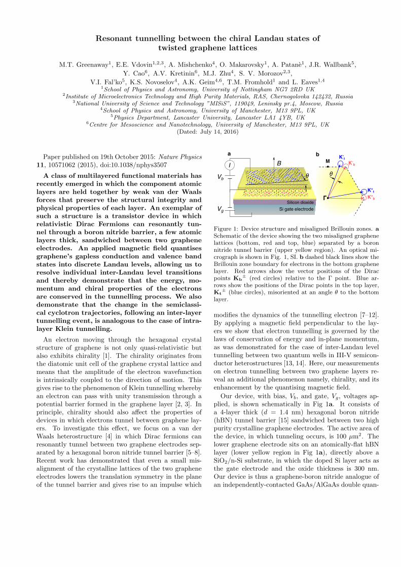
Figure 1: Device structure and misaligned Brillouin zones. aSchematic of the device showing the two misaligned graphenelattices (bottom, red and top, blue) separated by a boronnitride tunnel barrier (upper yellow region). An optical mi-crograph is shown in Fig. 1, SI. b dashed black lines show theBrillouin zone boundary for electrons in the bottom graphenelayer. Red arrows show the vector positions of the Diracpoints Kb
± (red circles) relative to the Γ point. Blue ar-rows show the positions of the Dirac points in the top layer,Kt
± (blue circles), misoriented at an angle θ to the bottomlayer.
modifies the dynamics of the tunnelling electron [7–12].By applying a magnetic field perpendicular to the lay-ers we show that electron tunnelling is governed by thelaws of conservation of energy and in-plane momentum,as was demonstrated for the case of inter-Landau leveltunnelling between two quantum wells in III-V semicon-ductor heterostructures [13, 14]. Here, our measurementson electron tunnelling between two graphene layers re-veal an additional phenomenon namely, chirality, and itsenhancement by the quantising magnetic field.
Our device, with bias, Vb, and gate, Vg, voltages ap-plied, is shown schematically in Fig 1a. It consists ofa 4-layer thick (d = 1.4 nm) hexagonal boron nitride(hBN) tunnel barrier [15] sandwiched between two highpurity crystalline graphene electrodes. The active area ofthe device, in which tunneling occurs, is 100 µm2. Thelower graphene electrode sits on an atomically-flat hBNlayer (lower yellow region in Fig 1a), directly above aSiO2/n-Si substrate, in which the doped Si layer acts asthe gate electrode and the oxide thickness is 300 nm.Our device is thus a graphene-boron nitride analogue ofan independently-contacted GaAs/AlGaAs double quan-
2
i
ΔKI (
μA)
0
10
20
30
40
600
500
400
100
300
G (μ
S)
b0 0.2 0.4 0.6 0.8
a
1
2
3
4
5
6x 10⁻⁴
ii eV2
eV1
V2
V1
200
-0.4 -0.3 -0.2 -0.1 0 0.1 0.2 0.3 0.4Vb (V)
-0.5 0.5
0
ΔK
kx
Eky
kx
Eky
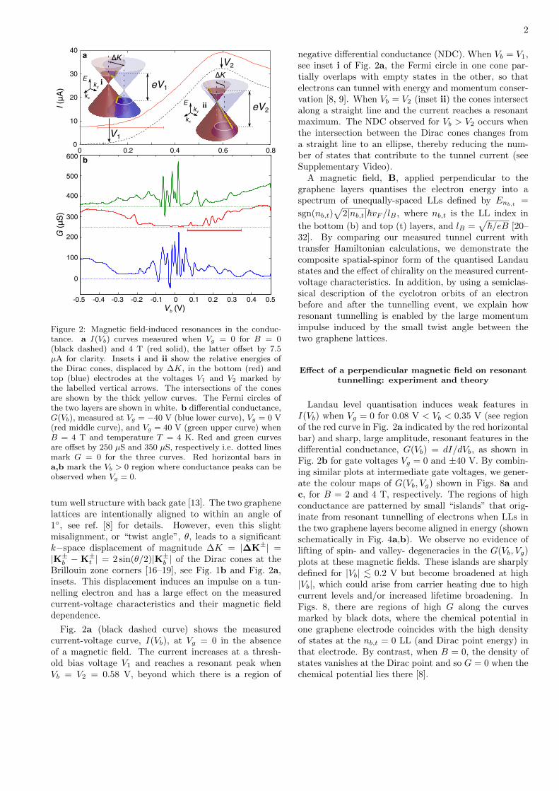
Figure 2: Magnetic field-induced resonances in the conduc-tance. a I(Vb) curves measured when Vg = 0 for B = 0(black dashed) and 4 T (red solid), the latter offset by 7.5µA for clarity. Insets i and ii show the relative energies ofthe Dirac cones, displaced by ∆K, in the bottom (red) andtop (blue) electrodes at the voltages V1 and V2 marked bythe labelled vertical arrows. The intersections of the conesare shown by the thick yellow curves. The Fermi circles ofthe two layers are shown in white. b differential conductance,G(Vb), measured at Vg = −40 V (blue lower curve), Vg = 0 V(red middle curve), and Vg = 40 V (green upper curve) whenB = 4 T and temperature T = 4 K. Red and green curvesare offset by 250 µS and 350 µS, respectively i.e. dotted linesmark G = 0 for the three curves. Red horizontal bars ina,b mark the Vb > 0 region where conductance peaks can beobserved when Vg = 0.
tum well structure with back gate [13]. The two graphenelattices are intentionally aligned to within an angle of1◦, see ref. [8] for details. However, even this slightmisalignment, or “twist angle”, θ, leads to a significantk−space displacement of magnitude ∆K = |∆K±| =|K±b − K±t | = 2 sin(θ/2)|K±b | of the Dirac cones at theBrillouin zone corners [16–19], see Fig. 1b and Fig. 2a,insets. This displacement induces an impulse on a tun-nelling electron and has a large effect on the measuredcurrent-voltage characteristics and their magnetic fielddependence.
Fig. 2a (black dashed curve) shows the measuredcurrent-voltage curve, I(Vb), at Vg = 0 in the absenceof a magnetic field. The current increases at a thresh-old bias voltage V1 and reaches a resonant peak whenVb = V2 = 0.58 V, beyond which there is a region of
negative differential conductance (NDC). When Vb = V1,see inset i of Fig. 2a, the Fermi circle in one cone par-tially overlaps with empty states in the other, so thatelectrons can tunnel with energy and momentum conser-vation [8, 9]. When Vb = V2 (inset ii) the cones intersectalong a straight line and the current reaches a resonantmaximum. The NDC observed for Vb > V2 occurs whenthe intersection between the Dirac cones changes froma straight line to an ellipse, thereby reducing the num-ber of states that contribute to the tunnel current (seeSupplementary Video).
A magnetic field, B, applied perpendicular to thegraphene layers quantises the electron energy into aspectrum of unequally-spaced LLs defined by Enb,t
=
sgn(nb,t)√
2|nb,t|~vF /lB , where nb,t is the LL index in
the bottom (b) and top (t) layers, and lB =√
~/eB [20–32]. By comparing our measured tunnel current withtransfer Hamiltonian calculations, we demonstrate thecomposite spatial-spinor form of the quantised Landaustates and the effect of chirality on the measured current-voltage characteristics. In addition, by using a semiclas-sical description of the cyclotron orbits of an electronbefore and after the tunnelling event, we explain howresonant tunnelling is enabled by the large momentumimpulse induced by the small twist angle between thetwo graphene lattices.
Effect of a perpendicular magnetic field on resonanttunnelling: experiment and theory
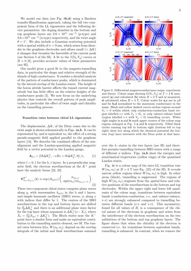
Landau level quantisation induces weak features inI(Vb) when Vg = 0 for 0.08 V < Vb < 0.35 V (see regionof the red curve in Fig. 2a indicated by the red horizontalbar) and sharp, large amplitude, resonant features in thedifferential conductance, G(Vb) = dI/dVb, as shown inFig. 2b for gate voltages Vg = 0 and ±40 V. By combin-ing similar plots at intermediate gate voltages, we gener-ate the colour maps of G(Vb, Vg) shown in Figs. 8a andc, for B = 2 and 4 T, respectively. The regions of highconductance are patterned by small “islands” that orig-inate from resonant tunnelling of electrons when LLs inthe two graphene layers become aligned in energy (shownschematically in Fig. 4a,b). We observe no evidence oflifting of spin- and valley- degeneracies in the G(Vb, Vg)plots at these magnetic fields. These islands are sharplydefined for |Vb| . 0.2 V but become broadened at high|Vb|, which could arise from carrier heating due to highcurrent levels and/or increased lifetime broadening. InFigs. 8, there are regions of high G along the curvesmarked by black dots, where the chemical potential inone graphene electrode coincides with the high densityof states at the nb,t = 0 LL (and Dirac point energy) inthat electrode. By contrast, when B = 0, the density ofstates vanishes at the Dirac point and so G = 0 when thechemical potential lies there [8].
3
We model our data (see Fig. 8b,d) using a Bardeentransfer-Hamiltonian approach, taking the full two com-ponent form of the LL eigenstates and the following de-vice parameters: the doping densities in the bottom andtop graphene layers are 2.0 × 1011 cm−2 (p-type) and3.6×1011 cm−2 (n-type) respectively, and the twist angleθ = 1◦. We also include a Gaussian scattering potentialwith a spatial width of σ = 9 nm, which arises from disor-der in the graphene electrodes and allows small (< ∆K)k changes that broaden the linewidth of the current peak(see Section 5 of the SI). A fit to the I(Vb, Vg) curves atB = 0 [8], provides accurate values of these parameters(see SI).
Our model gives a good fit to the magneto-tunnellingdata, in particular the shape and relative strength of theislands of high conductance. It enables a detailed analysisof the pattern of conductance peaks, which is dominatedby the lateral overlap of the Landau states. The height ofthe boron nitride barrier affects the tunnel current mag-nitude but has little effect on the relative heights of theconductance peaks [5]. We now focus on the underlyingphysics that controls the overall pattern of peak ampli-tudes, in particular the effect of twist angle and chiralityon the tunnelling process.
Transition rates between chiral LL eigenstates
The displacement, ∆K, of the Dirac cones due to thetwist angle is shown schematically in Figs. 4a,b. It can berepresented by, and is equivalent to, the effect of a strongpseudo-magnetic field applied parallel to the graphenelayers [14]. We describe the combined effects of the mis-alignment and the Landau-quantising applied magneticfield by a vector potential in the Landau gauge,
Ab,t =(l~∆K±x ,−eBx+ l~∆K±y , 0
)/e, (1)
where l = 0, 1 for the b, t layers. In a perpendicular mag-netic field, the electron wavefunctions at the K+ pointhave the analytic forms [22, 23]
ΨK+
nb,t,ky,b,t(r) ∝ exp (iky,b,t)
(φ|nb,t|
-sgn(nb,t)iφ|nb,t|−1
).
(2)These two-component chiral states comprise plane wavesalong y, with wavenumber ky,b,t in the b and t layers,and simple harmonic oscillator (SHO) waves, φ, along xwith indices that differ by 1. The centres of the SHOwavefunctions in the top and bottom layers are shiftedby l2B∆K+
y and there is an additional plane wave factorfor the top layer whose argument is ∆K+
x (x−Xt), whereXt = l2B(ky,t + ∆K+
y ). The Bloch states near the K−
point have a similar form and make an equivalent contri-bution to the tunnelling matrix element, see SI. The tun-nel rates between LLs, W (nb, nt), depend on the overlapintegrals of the initial and final wavefunctions summed
Vg (V
)
40
20
0
-20
-40
0 40 80 120
-0.4 0 0.4Vb (V)
0 0.4 0.8
-0.4 0 0.4Vb (V)
Vg (V
)
40
20
0
-20
-40
0 100 200 400300
-0.4 0 0.4Vb (V)
-0.4 0 0.4Vb (V)
0 0.4 0.8
a B = 2 T, experiment b B = 2 T, theory
c B = 4 T, experiment d B = 4 T, theory
v-v
c-c
v-v
c-c
v-v
c-c
v-vc-c
Figure 3: Differential magnetoconductance maps: experimentand theory. Colour maps showing G(Vb, Vg) at T = 4 K mea-sured (a) and calculated (b) when B = 2 T and (c measured,d calculated) when B = 4 T. Colour scales for a,c are in µSand for b,d normalised to the maximum conductance in themaps. Black and yellow dashed curves enclose regions aroundVb = 0 within which only conduction-conduction band (re-gion labelled c-c with Vg > 0), or only valence-valence band(region labelled v-v with Vg < 0) tunnelling occurs. Whiteright angles in a and b mark upper corners of the colour mapregions enlarged in Fig. 5 a and b respectively. Filled blackcircles running top left to bottom right (bottom left to topright) show loci along which the chemical potential the bot-tom (top) layer intersects with the Dirac point in that layer.
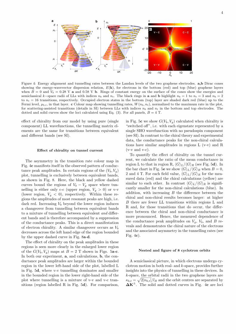
over the k−states in the two layers (see SI) and there-fore permits tunnelling between SHO states with a rangeof different n indices. Figs. 4a,b show the energies andsemiclassical trajectories (yellow rings) of the quantisedLandau states.
Fig. 4c is a colour map of the inter-LL transition rateW (nb, nt) at B = 4 T (see Eq. (25) of the SI). It revealsnarrow yellow regions where W (nb, nt) is high. In otherareas (black), tunnelling is suppressed. The regions ofhigh W (nb, nt) originate from the spatial form and rela-tive positions of the wavefunctions in the bottom and topelectrodes. Within the upper right and lower left quad-rants of the colour map, transitions between equivalentbands (conduction-conduction, c-c, and valence-valence,v-v) are strongly enhanced compared to tunnelling be-tween different bands (c-v and v-c). This asymmetry,found for all values of B, is a consequence of the chi-ral nature of the electrons in graphene and arises fromthe interference of the electron wavefunction on the twosublattices of the bottom and top graphene layers. Thefigure shows that when the chirality of the electron isconserved i.e. for transitions between equivalent bands,tunnelling is enhanced. In contrast, when we remove the
4
a
ΔK
E
μb
μt
01
23
4
0
-1-2
-3-4
1
ky
kx
b
E
μb
0
μt
ΔK
0
0
16
-7
ky
kx
2
4
6
2
nt
20
0
-10
-20
c
10
20100-20nb
-10
0 1
c - c
v - v c - v
v - c
Figure 4: Energy alignment and tunnelling rates between the Landau levels of the two graphene electrodes. a,b Dirac conesshowing the energy-wavevector dispersion relation, E(k), for electrons in the bottom (red) and top (blue) graphene layerswhen B = 0 and Vb = 0.28 V a and 0.58 V b. Rings of constant energy on the surface of the cones show the energies andsemiclassical k−space radii of LLs with indices nb and nt. The black rings in a and b highlight nb = 1 to nt = 3 and nb = 2to nt = 16 transitions, respectively. Occupied electron states in the bottom (top) layer are shaded dark red (blue) up to theFermi level, µb,t, in that layer. c Colour map showing tunnelling rates, W (nb, nt), normalized to the maximum rate in the plot,for scattering-assisted transitions (details in SI) between LLs with indices nb and nt in the bottom and top electrodes. Thedotted and solid curves show the loci calculated using Eq. (3). For all panels, B = 4 T.
effect of chirality from our model by using pure (singlecomponent) LL wavefunctions, the tunnelling matrix el-ements are the same for transitions between equivalentand different bands (see SI).
Effect of chirality on tunnel current
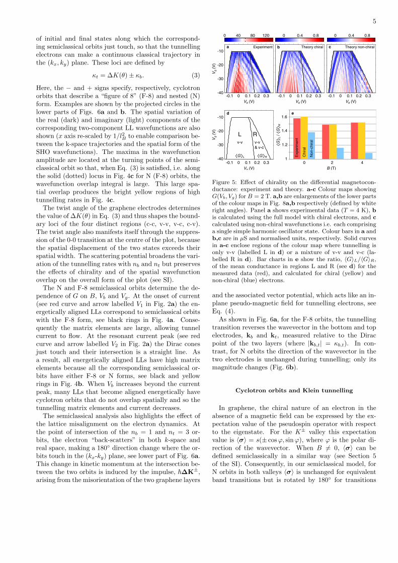
The asymmetry in the transition rate colour map inFig. 4c manifests itself in the observed pattern of conduc-tance peak amplitudes. In certain regions of the (Vb, Vg)plot, tunnelling is exclusively between equivalent bands,as shown in Fig. 8. Here, the black and yellow dashedcurves bound the regions of Vb − Vg space where tun-nelling is either only c-c (upper region, Vg > 0) or v-v(lower region, Vg < 0), respectively. Within these re-gions the amplitudes of most resonant peaks are high, i.e.dark red. Increasing Vb beyond the lower region inducesa changeover from tunnelling between equivalent bandsto a mixture of tunnelling between equivalent and differ-ent bands and is therefore accompanied by a suppressionof the conductance peaks. This is a direct manifestationof electron chirality. A similar changeover occurs as Vbdecreases across the left hand edge of the region boundedby the upper dashed curve in Fig. 8a-d.
The effect of chirality on the peak amplitudes in theseregions is seen more clearly in the enlarged lower regionof the G(Vb, Vg) maps at B = 2 T shown in Figs. 5a-c.In both our experiment, a, and calculations, b, the con-ductance peak amplitudes are larger within the boundedregion in the lower left-hand side of the plot, labelled Lin Fig. 5d, where v-v tunnelling dominates and smallerin the bounded region in the lower right-hand side of theplot where tunnelling is a mixture of v-v and v-c tran-sitions (region labelled R in Fig. 5d). For comparison,
in Fig. 5c we show G(Vb, Vg) calculated when chirality is“switched off”, i.e. with each eigenstate represented by asingle SHO wavefunction with no pseudospin component(see SI). In contrast to the chiral theory and experimentaldata, the conductance peaks for the non-chiral calcula-tions have similar amplitudes in regions L (v-v) and R(v-v and v-c).
To quantify the effect of chirality on the tunnel cur-rent, we calculate the ratio of the mean conductance inregion L to that in region R, 〈G〉L/〈G〉R (see Fig. 5d). Inthe bar chart in Fig. 5e we show 〈G〉L/〈G〉R when B = 0,2 and 4 T. For each field value, 〈G〉L/〈G〉R for the mea-sured data (red) and the chiral calculations (yellow) aresimilar to each other. In contrast 〈G〉L/〈G〉R is signifi-cantly smaller for the non-chiral calculations (blue). Inaddition, with increasing B the difference between thechiral and non-chiral results becomes larger: at higherB there are fewer LL transitions within regions L andR and, for those transitions that do occur, the differ-ence between the chiral and non-chiral conductance ismore pronounced. Hence, the measured dependence ofthe conductance peak amplitudes on Vg, Vb, and B re-veals and demonstrates the chiral nature of the electronsand the associated asymmetry in the tunnelling rates (seeFig. 4c).
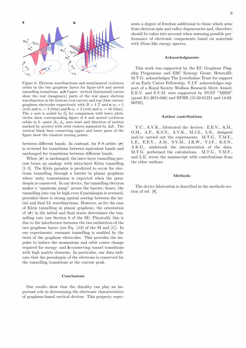
Nested and figure of 8 cyclotron orbits
A semiclassical picture, in which electrons undergo cy-clotron motion in both real- and k-space, provides furtherinsights into the physics of tunnelling in these devices. Ink-space, the orbital radii in the two graphene layers areκb,t =
√2|nb,t|/lB and the orbit centres are separated by
∆K±. The solid and dotted curves in Fig. 4c are loci
5
of initial and final states along which the correspond-ing semiclassical orbits just touch, so that the tunnellingelectrons can make a continuous classical trajectory inthe (kx, ky) plane. These loci are defined by
κt = ∆K(θ)± κb. (3)
Here, the − and + signs specify, respectively, cyclotronorbits that describe a “figure of 8” (F-8) and nested (N)form. Examples are shown by the projected circles in thelower parts of Figs. 6a and b. The spatial variation ofthe real (dark) and imaginary (light) components of thecorresponding two-component LL wavefunctions are alsoshown (x axis re-scaled by 1/l2B to enable comparison be-tween the k-space trajectories and the spatial form of theSHO wavefunctions). The maxima in the wavefunctionamplitude are located at the turning points of the semi-classical orbit so that, when Eq. (3) is satisfied, i.e. alongthe solid (dotted) locus in Fig. 4c for N (F-8) orbits, thewavefunction overlap integral is large. This large spa-tial overlap produces the bright yellow regions of hightunnelling rates in Fig. 4c.
The twist angle of the graphene electrodes determinesthe value of ∆K(θ) in Eq. (3) and thus shapes the bound-ary loci of the four distinct regions (c-c, v-v, v-c, c-v).The twist angle also manifests itself through the suppres-sion of the 0-0 transition at the centre of the plot, becausethe spatial displacement of the two states exceeds theirspatial width. The scattering potential broadens the vari-ation of the tunnelling rates with nb and nt but preservesthe effects of chirality and of the spatial wavefunctionoverlap on the overall form of the plot (see SI).
The N and F-8 semiclassical orbits determine the de-pendence of G on B, Vb and Vg. At the onset of current(see red curve and arrow labelled V1 in Fig. 2a) the en-ergetically aligned LLs correspond to semiclassical orbitswith the F-8 form, see black rings in Fig. 4a. Conse-quently the matrix elements are large, allowing tunnelcurrent to flow. At the resonant current peak (see redcurve and arrow labelled V2 in Fig. 2a) the Dirac conesjust touch and their intersection is a straight line. Asa result, all energetically aligned LLs have high matrixelements because all the corresponding semiclassical or-bits have either F-8 or N forms, see black and yellowrings in Fig. 4b. When Vb increases beyond the currentpeak, many LLs that become aligned energetically havecyclotron orbits that do not overlap spatially and so thetunnelling matrix elements and current decreases.
The semiclassical analysis also highlights the effect ofthe lattice misalignment on the electron dynamics. Atthe point of intersection of the nb = 1 and nt = 3 or-bits, the electron “back-scatters” in both k-space andreal space, making a 180◦ direction change where the or-bits touch in the (kx-ky) plane, see lower part of Fig. 6a.This change in kinetic momentum at the intersection be-tween the two orbits is induced by the impulse, ~∆K±,arising from the misorientation of the two graphene layers
0.15
V g (V
)
-10
-20
-30
-40
a
0 40 80 120 0 0.80.4
b c
Vb (V)0-0.1 0.1 0.2 0.3
0 0.80.4
Vb (V)0-0.1 0.1 0.2 0.3
Vb (V)0-0.1 0.1 0.2 0.3
v-v v-v& v-c
V g (V
)
-10
-20
-30
-40
Vb (V)0-0.1 0.1 0.2 0.3
B (T)0 2 4
1
1.2
1.4
1.6
⟨G⟩ L
/ ⟨G
⟩ R
d e
L R
⟨G⟩R⟨G⟩L
Experiment Theory chiral Theory non-chiral
Expe
rimen
t
Chi
ral
Non
-chi
ral
Figure 5: Effect of chirality on the differential magnetocon-ductance: experiment and theory. a-c Colour maps showingG(Vb, Vg) for B = 2 T. a,b are enlargements of the lower partsof the colour maps in Fig. 8a,b respectively (defined by whiteright angles). Panel a shows experimental data (T = 4 K), bis calculated using the full model with chiral electrons, and ccalculated using non-chiral wavefunctions i.e. each comprisinga single simple harmonic oscillator state. Colour bars in a andb,c are in µS and normalised units, respectively. Solid curvesin a-c enclose regions of the colour map where tunnelling isonly v-v (labelled L in d) or a mixture of v-v and v-c (la-belled R in d). Bar charts in e show the ratio, 〈G〉L/〈G〉R,of the mean conductance in regions L and R (see d) for themeasured data (red), and calculated for chiral (yellow) andnon-chiral (blue) electrons.
and the associated vector potential, which acts like an in-plane pseudo-magnetic field for tunnelling electrons, seeEq. (4).
As shown in Fig. 6a, for the F-8 orbits, the tunnellingtransition reverses the wavevector in the bottom and topelectrodes, kb and kt, measured relative to the Diracpoint of the two layers (where |kb,t| = κb,t). In con-trast, for N orbits the direction of the wavevector in thetwo electrodes is unchanged during tunnelling; only itsmagnitude changes (Fig. 6b).
Cyclotron orbits and Klein tunnelling
In graphene, the chiral nature of an electron in theabsence of a magnetic field can be expressed by the ex-pectation value of the pseudospin operator with respectto the eigenstate. For the K± valley this expectationvalue is 〈σ〉 = s(± cosϕ, sinϕ), where ϕ is the polar di-rection of the wavevector. When B 6= 0, 〈σ〉 can bedefined semiclassically in a similar way (see Section 5of the SI). Consequently, in our semiclassical model, forN orbits in both valleys 〈σ〉 is unchanged for equivalentband transitions but is rotated by 180◦ for transitions
6
a b
x/l 2BΨRe
ΨIm
kb
kb
x/l 2BΨRe
ΨIm
ky
kx
B
ky
kx
B
Figure 6: Electron wavefunctions and semiclassical cyclotronorbits in the two graphene layers for figure-of-8 and nestedtunnelling transitions. a,b Upper: vertical (horizontal) curvesshow the real (imaginary) parts of the real space electronwavefunction in the bottom (red curves) and top (blue curves)graphene electrodes respectively with B = 4 T and a nb = 1(red) and nt = 3 (blue) and b nb = 2 (red) and nt = 16 (blue).The x axis is scaled by l2B for comparison with lower plots:circles show corresponding figure of 8 and nested cyclotronorbits in k- space (kx, ky axes inset and direction of motionmarked by arrows) with orbit centres separated by ∆K. Thevertical black lines connecting upper and lower parts of thefigure show the classical turning points.
between different bands. In contrast, for F-8 orbits 〈σ〉is reversed for transitions between equivalent bands andunchanged for transitions between different bands.
When 〈σ〉 is unchanged, the inter-layer tunnelling pro-cess bears an analogy with intra-layer Klein tunnelling[1–3]. The Klein paradox is predicted to occur for elec-trons tunnelling through a barrier in planar graphenewhere unity transmission is expected when the pseu-dospin is conserved. In our device, the tunnelling electronmakes a “quantum jump” across the barrier; hence, thetunnelling rate can be high even if pseudospin is reversed,provided there is strong spatial overlap between the ini-tial and final LL wavefunctions. However, as for the caseof Klein tunnelling in planar graphene, the orientationof 〈σ〉 in the initial and final states determines the tun-nelling rate (see Section 6 of the SI). Physically this isdue to the interference between the two sublattices of thetwo graphene layers (see Eq. (13) of the SI and [1]). Inour experiments, resonant tunnelling is enabled by thetwist of the graphene electrodes. This provides the im-pulse to induce the momentum and orbit centre changerequired for energy- and k-conserving tunnel transitionswith high matrix elements. In particular, our data indi-cate that the pseudospin of the electrons is conserved forthe tunnelling transitions at the current peak.
Conclusions
Our results show that the chirality can play an im-portant role in determining the electronic characteristicsof graphene-based vertical devices. This property repre-
sents a degree of freedom additional to those which arisefrom electron spin and valley degeneracies and, therefore,should be taken into account when assessing possible per-formance of electronic components based on materialswith Dirac-like energy spectra.
Acknowledgments
This work was supported by the EU Graphene Flag-ship Programme and ERC Synergy Grant, Hetero2D.M.T.G. acknowledges The Leverhulme Trust for supportof an Early Career Fellowship. V.I.F. acknowledges sup-port of a Royal Society Wolfson Research Merit Award.E.E.V. and S.V.M. were supported by NUST ”MISiS”(grant K1-2015-046) and RFBR (15-02-01221 and 14-02-00792).
Author contributions
Y.C., A.V.K., fabricated the devices. E.E.V., A.M.,O.M., A.P., K.S.N., A.V.K., M.J.Z., L.E., designedand/or carried out the experiments. M.T.G., T.M.F.,L.E., E.E.V., A.M., S.V.M., J.R.W., V.I.F., K.S.N.,A.K.G., undertook the interpretation of the data.M.T.G. performed the calculations. M.T.G., T.M.F.,and L.E. wrote the manuscript with contributions fromthe other authors.
Methods
The device fabrication is described in the methods sec-tion of ref. [8].
7
SUPPLEMENTARY INFORMATION
DEVICE GEOMETRY
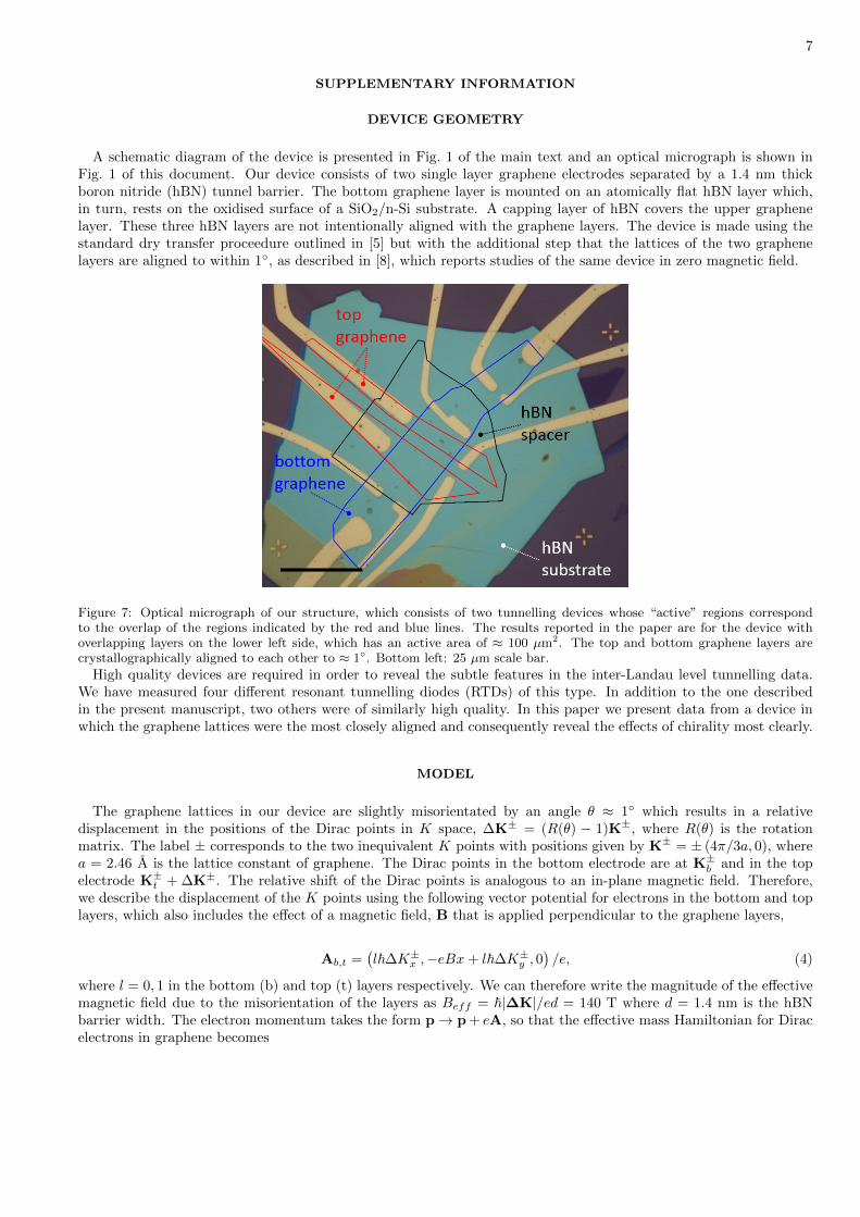
A schematic diagram of the device is presented in Fig. 1 of the main text and an optical micrograph is shown inFig. 1 of this document. Our device consists of two single layer graphene electrodes separated by a 1.4 nm thickboron nitride (hBN) tunnel barrier. The bottom graphene layer is mounted on an atomically flat hBN layer which,in turn, rests on the oxidised surface of a SiO2/n-Si substrate. A capping layer of hBN covers the upper graphenelayer. These three hBN layers are not intentionally aligned with the graphene layers. The device is made using thestandard dry transfer proceedure outlined in [5] but with the additional step that the lattices of the two graphenelayers are aligned to within 1◦, as described in [8], which reports studies of the same device in zero magnetic field.
Figure 7: Optical micrograph of our structure, which consists of two tunnelling devices whose “active” regions correspondto the overlap of the regions indicated by the red and blue lines. The results reported in the paper are for the device withoverlapping layers on the lower left side, which has an active area of ≈ 100 µm2. The top and bottom graphene layers arecrystallographically aligned to each other to ≈ 1◦. Bottom left: 25 µm scale bar.
High quality devices are required in order to reveal the subtle features in the inter-Landau level tunnelling data.We have measured four different resonant tunnelling diodes (RTDs) of this type. In addition to the one describedin the present manuscript, two others were of similarly high quality. In this paper we present data from a device inwhich the graphene lattices were the most closely aligned and consequently reveal the effects of chirality most clearly.
MODEL
The graphene lattices in our device are slightly misorientated by an angle θ ≈ 1◦ which results in a relativedisplacement in the positions of the Dirac points in K space, ∆K± = (R(θ) − 1)K±, where R(θ) is the rotationmatrix. The label ± corresponds to the two inequivalent K points with positions given by K± = ± (4π/3a, 0), wherea = 2.46 A is the lattice constant of graphene. The Dirac points in the bottom electrode are at K±b and in the topelectrode K±t + ∆K±. The relative shift of the Dirac points is analogous to an in-plane magnetic field. Therefore,we describe the displacement of the K points using the following vector potential for electrons in the bottom and toplayers, which also includes the effect of a magnetic field, B that is applied perpendicular to the graphene layers,
Ab,t =(l~∆K±x ,−eBx+ l~∆K±y , 0
)/e, (4)
where l = 0, 1 in the bottom (b) and top (t) layers respectively. We can therefore write the magnitude of the effectivemagnetic field due to the misorientation of the layers as Beff = ~|∆K|/ed = 140 T where d = 1.4 nm is the hBNbarrier width. The electron momentum takes the form p→ p + eA, so that the effective mass Hamiltonian for Diracelectrons in graphene becomes
8
H±b,t = vF
(0 ± (px + eAx,b,t)− i (py + eAy,b,t)
± (px + eAx,b,t) + i (py + eAy,b,t) 0
), (5)
where vF = 106 ms−1. The Hamiltonian has the form of a quantum harmonic oscillator so that the electron hasdiscrete Landau energy levels given by
E2nb,t
= sgn(nb,t)|nb,t|2eB~v2F , (6)
where nb,t is an integer that labels the energy levels in the two electrodes, positive for electrons in the conductionband and negative in the valence band and
sgn(n) =
1 (n > 0)
0 (n = 0)
−1 (n < 0).
(7)
The electron wavefunctions at the two Dirac points are therefore
ΨK+
nb,t,ky,b,t(r) =
Cnb,t√L
exp (iky,b,ty)
(φ|nb,t|
-sgn(nb,t)iφ|nb,t|−1
)(8)
and
ΨK−
nb,t,ky,b,t(r) =
Cnb,t√L
exp (iky,b,ty)
(sgn(nb,t)iφ|nb,t|−1
φ|nb,t|
), (9)
where
Cn =
{1 (n = 0)
1/√
2 (n 6= 0)(10)
where
φ|nb| =1√
2|nb||nb|!√πlB
exp
[− 1
2l2B(x−Xb)
2
]H|nb|
(1
lB(x−Xb)
), (11)
and
φ|nt| =1√
2|nt||nt|!√πlB
exp
[− 1
2l2B(x−Xt)
2 − i∆K±x (x−Xt)
]H|nt|
(1
lB(x−Xt)
), (12)
Here lB =√
~/eB and Hn is the nth order Hermite polynomial. These two-component chiral states comprise planewaves along y, with wavenumber ky,b,t in the b and t layers, and simple harmonic oscillator (SHO) waves, φ, alongx with indices that differ by 1. The orbit centre in the bottom and top electrodes are given by Xb = l2Bky,b andXt = l2B(ky,t + ∆K±y ) respectively. The effect of the misorientation of the two graphene sheets is to shift the relativeposition of their orbit centres by l2B∆K±y and introduce a phase difference of ∆Kx(x−Xt).
Matrix element
We assume that electrons can undergo elastic scattering which we describe using a Gaussian scattering potential:
VS(x, y) = V0e−x2/2σ2
s−y2/2σ2
s , (13)
9
where σs ≈ 10 nm is the scattering length scale. This value of σs agrees with values reported in the literature (Ref.[6] and references therein) and gives the best fit to the line width of the peak in the current-voltage curve when B = 0[8]. The matrix element for tunnelling between the bottom and top electrodes is given by
Mbt =
∫V
dVΨ∗t (r, z)VSΨb(r, z). (14)
First we consider the integral in the z direction. We assume that the electron wavefunctions decay exponentially intothe barrier regions so that the integral is a constant, equal to
Ξ =V0De−κd. (15)
where d is the barrier width. We assume κ to be independent of energy to facilitate analysis of the current. For fullanalysis of different Vb dependent models for κ, see Ref. [5]. In the basis of Bloch wavefunctions [8, 9], the matrixelement is given by
Mbt(nb, nt, ky,b, ky,t) =1
LCnb
CntΞIy(ky,b, ky,t) [Ix(|nb|, |nt|, ky,b, ky,t)∓ isgn(nb)Ix(|nb| − 1, |nt|, ky,b, ky,t)
±isgn(nb)Ix(|nb|, |nt| − 1, ky,b, ky,t) + sgn(nb)sgn(nT )Ix(|nb| − 1, |nt| − 1, ky,b, ky,t)] (16)
where Ix and Iy are the overlap integrals of the wavefunctions along the x and y axes respectively. On firstinspection, Eq. (16) appears to reveal that the matrix element is different for tunnelling between K+ valleys (uppersign) compared to that between K− valleys (lower sign). However, ∆K+ = −∆K− and, consequently, it can beshown that the matrix element for transitions between the same valleys are equivalent. Our matrix element doesnot explicitly include the cell-periodic parts of the Bloch functions, uα,β(r), where α and β label the two atoms ingrahene’s unit cell. This is because for small relative rotations of the two layers, the spatial overlap integral of thecell-periodic parts of the wavefunction
∫dSu∗α,β(R(θ)r)uα,β(r) are approximately equivalent for all combinations of
α and β, and therefore will only have a small quantitative effect on the matrix element [9].
Overlap integrals for scattering assisted tunnelling
The overlap integrals Iy and Ix can be shown [33] to have following form:
Iy =√
2πσs exp(−∆k2σ2
s/2), (17)
within which ∆k = ky,b − ky,t. The overlap integral in the x direction, Ix, is given by:
Ix (nb, nt, ky,b, ky,t) =1
ζlBPbt (nb, nt, ky,b, ky,t)
bnb,ntc∑j=0
j!
(nbj
)(ntj
)(1− a2
)(nb+nt)/2−j × (18)
(2a2)jHnb−j
[aΥ− lBky,b(1− a2)
1/2
]Hnt−j
[aΥ− lB
(ky,t + ∆K+
y
)(1− a2) 1/2
](19)
where a = 1/ζlB ,
ζ2 =
(1
l2B+
1
2σ2s
), (20)
Pbt (nb, nt, ky,b,t) =exp [ϑ (ky,b, ky,t)]√
2ntnt!2nbnb!, (21)
10
within which
ϑ = Υ2 − l2B2
((ky,t + ∆K±y
)2+ k2y,b
)− i∆K±x
(ky,t + ∆K±y
), (22)
and
Υ =1
2ζ
(ky,t + ∆K±y + ky,b + i∆K±x
). (23)
Current
Expression for the tunnel current
The current between the layers is given by the sum over states in the top and bottom layers:
I = gV4πe
~∑bt
|Mbt|2 [fb(Eb)− ft(Et)] δ(Eb − Et), (24)
where the Fermi functions for the bottom and top layers are given, respectively, by
fb(Eb) =1
1 + e(Eb−µb)/kBT(25)
and
ft(Et) =1
1 + e(Et−µt)/kBT. (26)
and kBT is the thermal energy. We assume that the Landau levels (LLs) are broadened in energy by Γb,t in thebottom and top electrodes respectively due to electron - electron interactions, which we model with a set of Gaussianfunctions (to ensure convergence at low magnetic fields) centered on the energies of the LLs En (see Eq. (6)) [21]
Γ (E) =
∞∑n=−∞
1√2πΓb,t
exp
(− (E − En)
2
2Γ2b,t
). (27)
The density of states is then given by D(E) = (2/πl2B)Γ(E). We convert the sum over k−states in Eq. (24) to anintegral to find the contribution to the current for transitions between LLs nt and nb is given by
W (nb, nt) =2L4
π2l4B
∫ ∫|Mbt|2dky,bdky,t, (28)
where L is the device length, so that after using the δ function to integrate out Et, we find that the current can nowbe expressed by:
I = gV4πe
~
∫W (nb, nt) [fb(Eb)− ft(Et)]Db(Eb)Dt(Eb − φ)dEb. (29)
Form of the tunnel current versus bias voltage curve for B = 0
A detailed analysis of the form of the I(Vb) curve for B = 0 is given in Ref. [8]. In the Supplementary Video (SV)we present an animation, which shows how the key features in the measured (red) and modeled, with momentumconserving transitions only (σs → ∞, blue), I(Vb) curves relate to the form of the intersection (shown yellow in theSV) between the two Dirac cones as they move relative to one another in response to changes in Vb.
11
Electrostatic model
We model the electrostatics, i.e. the values of µb,t and the electrostatic potential energy difference φb between thegraphene layers, by solving the following equation:
φ+ µt(ρt,Γt)− µb(ρb,Γb) + eVb = 0 (30)
where d = 1.4 nm is the barrier width, ρb,t is the charge density on the bottom and top electrodes and the functionµ(ρ,Γ) is found using the density of states, D(E) [5]. From Gauss’s law, and ensuring charge neutrality, we obtainthe following relationships between Vb, Vg, φ and nb,t:
ε (Fb − Fg) = ρb (31)
−εFb = ρt, (32)
where Fb = φb/ed and Fg = (eVg − µb)/eDg are the fields in the tunnel barrier and gate-oxide barrier respectivelyand Dg = 300 nm is the oxide thickness.
ANALYSIS OF CONDUCTANCE PEAKS
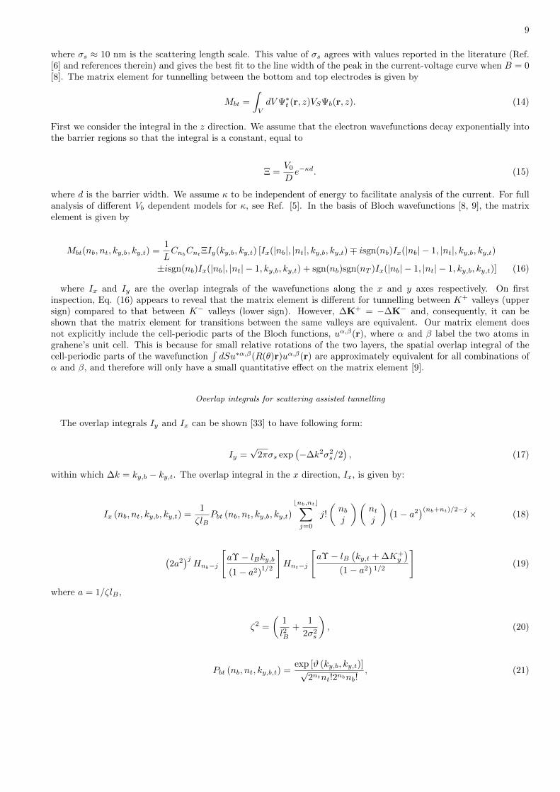
Fig. 8 shows colour maps of G(Vb, Vg) = dI/dVb measured (a,c) and calculated (b, d) when B = 2 T (a,b) andB = 4 T (c,d). The parameters used to model the measured data are σs = 9 nm and the LL broadening in the bottomand top graphene electrodes, Γb and Γt, is set at 4 meV and 4 meV (6 meV and 8 meV) respectively when B = 2 T (4T). Note that we focus on magnetic field values ≤ 4T because higher fields lead to a strong in-plane magnetoresistancein the sections of the graphene layers that carry the current to the active tunnelling area of the device. Althoughresonant peaks due to inter-Landau level tunnelling are observed at these higher fields, their voltage positions aresignificantly displaced due to the magnetoresistance, making it difficult to interpret the data and compare it withtheory.
In this section we explain in more detail the origin of the conductance peaks observed in G(Vb, Vg). The filled blackcircles in Fig. 8 show the calculated (Vb, Vg) loci for which the chemical potential in the top layer intersects withthe zeroth LL in that layer, see inset A (filled circles running bottom left to top right), and for which the chemicalpotential in the bottom layer coincides with the zeroth LL in the bottom layer, see inset B (filled circles runningtop left to bottom right). Therefore, the local conductance peaks that lie along the X-shaped loci correspond to thealignment of the chemical potential in one graphene layer with the peak in the density of states for the LL at theDirac point.
Fig. 8 shows that in both our experiments and theory, when Vg ≈ 5 V and Vb . 0.2 V, increasing Vb initially haslittle effect on G. But when Vb ≈ ±0.2 V, there is a sharp increase in conductance. When Vb increases beyond ≈ 0.5V, G decreases, becoming negative after the peak in I(Vb). The regions of high G in Fig. 8 form stripe patternswith similar shapes to the loci marked by the filled circles. This is because they also originate from alignment of thechemical potential and LLs when µb,t = Enb,t
where, in contrast to the yellow curves, nb,t 6= 0. The crossing of theseloci gives rise to more islands of high G, for example those labelled “B-D” in Fig. 8 c,d.
When B = 4 T, we find good qualitative agreement between the measured and calculated G(Vb, Vg) colour maps.Along the loci marked by filled circles in Fig. 8c both maps reveal a series of conductance maxima in similar positions,for example those labelled “B-D” in Fig. 8c and d. As explained above, along the loci, the maxima occur as µt sweepsthrough the LL spectra in the top and bottom layers. The maxima labelled “B” and “C” occur when µt coincideswith nt = −1 and nt = −2 LLs (see insets labelled “B” and “C”). The strength of the maxima depends on thealignment of the LLs. For example, the conductance maximum labelled “D” is stronger than “B”, because at “B”the LL spectra in the top and bottom layers are aligned and tunnelling occurs from nb = 0 and −1 to nt = 0 and −1,which have low matrix elements (see main text) By contrast, for case “D” the matrix element for tunnelling betweenthe energetically aligned LLs nb = 3 and nt = 1 is high.
Conductance peaks for Vg < 0
We now analyse the features that appear in the G(Vb, Vg) colour maps at low |Vb| . 0.2 V for Vg < 0 when B= 2 T and 4 T. These features occur whenever the chemical potential in either the bottom or top layer is aligned
12
V g (V
)
40
20
0
-20
-40
0 40 80 120
-0.4 0 0.4Vb (V)
a
V g (V
)40
20
0
-20
-40
0 100 200 400300
-0.4 0 0.4Vb (V)
c
-0.4 0 0.4Vb (V)
d
0 0.4
-0.4 0 0.4Vb (V)
b
0.8
0 0.4 0.8
B CD
A
E
D
CB DA
B CD
A
Figure 8: Colour maps showing G(Vb, Vg) measured (a) and calculated (b) when B = 2 T and when B = 4 T (c measured,d calculated). Colour scales for a,c (b,d) are in µS (arbitrary units). Black and white dashed curves enclose islands withinwhich only conduction-conduction (Vg > 0) or valence-valence (Vg < 0) tunnelling occurs. Filled black circles running top leftto bottom right (bottom left to top right) show loci along which the chemical potential the bottom (top) layer intersects withthe Dirac point in that layer. Lower panels A-D show the density of states, D, calculated versus energy, E, in the bottom(red) and top (blue) graphene electrodes and correspond to the features labelled A-D in colour maps c and d. Horizontal redand blue dashed lines show position of the chemical potentials in the bottom and top electrodes.
energetically with one of the LLs in the top or bottom layer respectively. The resulting local maxima in G(Vb, Vg)occur at similar positions in the measured (Figs. 8a,c) and calculated (Figs. 8b,d) colour maps. However, whenB = 2 T, the theoretical results reveal many more features than the measured data. This is because our calculationsassume a constant LL width and therefore omit the increased LL broadening that could occur at high Vb in the actualdevice, e.g. due to electron heating. However, the general features of the measured and calculated colour maps aresimilar, in particular the positions of the resonant peaks and the width and shape of the X-shaped low G region.
In Figs. 9a and b we show an enlargement of Fig. 8c and d focusing on the series of conductance peaks foundfor low Vb and negative Vg when B = 4 T. To model the data at low Vb, where electron heating is low, we use anarrower broadening (Γb = 3 meV and Γt = 5 meV) than used for the full range of bias voltage. There is verygood correspondence of the positions of the peaks in the modelled and measured data. As for the local conductancepeaks considered previously, the peaks arise from a series of alignments of LLs of different index and the alignmentsof the chemical potentials. To aid understanding of these features we highlight two series of resonant peaks labelled,respectively, “A-F” and “i-v” showing the alignment of the LLs and the position of the chemical potentials in thegraphene layers.
MODEL FOR NON-CHIRAL ELECTRONS
To understand the effect of pseudospin on our conductance calculations, in this section we derive a model for non-chiral electrons. This model has the same structure as that presented for chiral electrons except that the electron
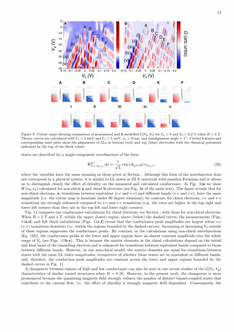
13
A B C D E F
i ii iii iv v
AB C
DE(i)
(ii)(iii)
(iv)(v)
F
-0.15 -0.1 -0.05 0 0.05 0.1 0.15 0.2
Vb (V)
A BC D
E(i)(ii)
(iii)(iv)(v)
F
-0.15 -0.1 -0.05 0 0.05 0.1 0.15 0.2
-20
-15
-10
-5
0
-25
-30
-35
-40
Vb (V)
V g (V
)G
(arb. units)
a b
Figure 9: Colour maps showing comparison of a measured and b modelled G(Vg, Vb) for Vg < 0 and Vb < 0.2 V when B = 4 T.Theory curves are calculated with Γb = 3 meV and Γt = 5 meV, σs = 9 nm, and misalignment angle = 1◦. Circled features andcorresponding inset plots show the alignments of LLs in bottom (red) and top (blue) electrodes with the chemical potentialsindicated by the top of the block colour.
states are described by a single-component wavefunction of the form
ΨK+
nb,t,ky,b,t(r) =
1√L
exp (iky,b,ty)φ|nb,t|, (33)
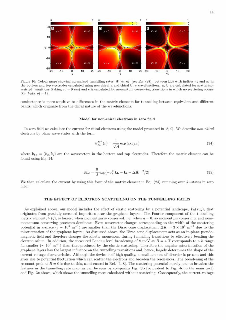
where the variables have the same meaning as those given in Section . Although this form of the wavefunction doesnot correspond to a physical system, it is similar to LL states in III-V materials with massless Fermions and it allowsus to distinguish clearly the effect of chirality on the measured and calculated conductance. In Fig. 10a we showW (nb, nt) calculated for non-chiral a and chiral b electrons (see Fig. 3c of the main text). The figure reveals that fornon-chiral electrons, a, transitions between equivalent (c-c and v-v) and different bands (v-c and c-v), have the samemagnitude (i.e. the colour map is invariant under 90 degree rotations); by contrast, for chiral electrons, c-c and v-vtransitions are strongly enhanced compared to v-c and c-v transitions (e.g. the rates are higher in the top right andlower left corners than they are in the top left and lower right corners).
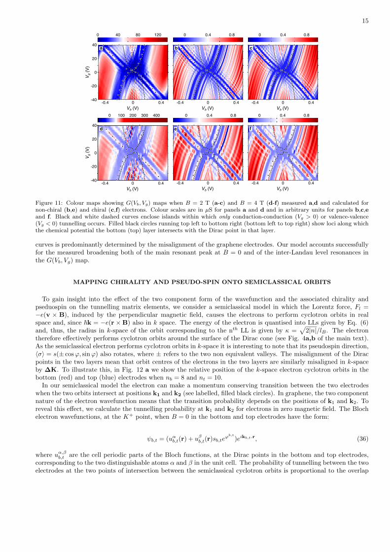
Fig. 11 compares our conductance calculations for chiral electrons, see Section , with those for non-chiral electrons.When B = 2 T and 4 T, within the upper (lower) region, above (below) the dashed curves, the measurements (Figs.11a,d) and full chiral calculations (Figs. 11c,f) reveal that the conductance peak amplitudes are largest where c-c(v-v) transitions dominate (i.e. within the regions bounded by the dashed curves). Increasing or decreasing Vb outsideof these regions suppresses the conductance peaks. By contrast, in the calculations using non-chiral wavefunctions[Eq. (33)], the conductance peaks in the lower and upper regions have an almost constant amplitude over the wholerange of Vb (see Figs. 11b,e). This is because the matrix elements in the chiral calculations depend on the initialand final band of the tunnelling electron and is enhanced for transitions between equivalent bands compared to thosebetween different bands. However, in our non-chiral model, the matrix elements are equal for transitions betweenstates with the same LL index magnitudes, irrespective of whether those states are in equivalent or different bands,and, therefore, the conduction peak amplitudes are constant across the lower and upper regions bounded by thedashed curves in Fig. 11.
A changeover between regions of high and low conductance can also be seen in our recent studies of the G(Vb, Vg)characteristics of similar tunnel structures when B = 0 [8]. However, in the present work, the changeover is morepronounced because the quantising magnetic field strongly reduces the number of distinct tunnel-coupled states thatcontribute to the current flow; i.e. the effect of chirality is strongly magnetic field dependent. Consequently, the
14
nt
20
0
-10
-20
10
-20
a
20100nb
-10
0 1
c - c
v - v c - v
v - cb
20100-20nb
-10
0 1
c - c
v - v c - v
v - cc
20100-20nb
-10
0 1
c - c
v - v c - v
v - c
Figure 10: Colour maps showing normalised tunnelling rates, W (nb, nt) [see Eq. (28)], between LLs with indices nb and nt inthe bottom and top electrodes calculated using non chiral a and chiral b, c wavefunctions. a, b are calculated for scattering-assisted transitions (taking σs = 9 nm) and c is calculated for momentum conserving transitions in which no scattering occurs(i.e. VS(x, y) = 1).
conductance is more sensitive to differences in the matrix elements for tunnelling between equivalent and differentbands, which originate from the chiral nature of the wavefunctions.
Model for non-chiral electrons in zero field
In zero field we calculate the current for chiral electrons using the model presented in [8, 9]. We describe non-chiralelectrons by plane wave states with the form
ΨK+
kb,t(r) =
1√A
exp (ikb,t.r) (34)
where kb,t = (kx, ky) are the wavevectors in the bottom and top electrodes. Therefore the matrix element can befound using Eq. 14:
Mbt =Ξ
Aexp(−σ2
s |kb − kt −∆K±|2/2). (35)
We then calculate the current by using this form of the matrix element in Eq. (24) summing over k−states in zerofield.
THE EFFECT OF ELECTRON SCATTERING ON THE TUNNELLING RATES
As explained above, our model includes the effect of elastic scattering by a potential landscape, VS(x, y), thatoriginates from partially screened impurities near the graphene layers. The Fourier component of the tunnellingmatrix element, V (q), is largest when momentum is conserved, i.e. when q = 0, so momentum conserving and near-momentum conserving processes dominate. Even wavevector changes corresponding to the width of the scatteringpotential in k-space (q ∼ 108 m−1) are smaller than the Dirac cone displacement ∆K ∼ 3 × 10⁸ m−1 due to themisorientation of the graphene layers. As discussed above, the Dirac cone displacement acts as an in-plane pseudo-magnetic field and therefore changes the kinetic momentum during tunnelling transitions by effectively bending theelectron orbits. In addition, the measured Landau level broadening of 8 meV at B = 4 T corresponds to a k rangefar smaller (∼ 107 m−1) than that produced by the elastic scattering. Therefore the angular misorientation of thegraphene layers has the largest influence on the tunnelling transitions and, hence, largely determines the shape of thecurrent-voltage characteristics. Although the device is of high quality, a small amount of disorder is present and thisgives rise to potential fluctuation which can scatter the electrons and broaden the resonances. The broadening of theresonant peak at B = 0 is due to this, as discussed in Ref. [6, 8]. The scattering potential merely acts to broaden thefeatures in the tunnelling rate map, as can be seen by comparing Fig. 3b (equivalent to Fig. 4c in the main text)and Fig. 3c above, which shows the tunnelling rates calculated without scattering. Consequently, the current-voltage
15
V g (V
)
40
20
0
-20
-40
0 40 80 120
-0.4 0 0.4Vb (V)
a
0 0.4 0.8
-0.4 0 0.4Vb (V)
c
V g (V
)
40
20
0
-20
-40
0 100 200 400300
-0.4 0 0.4Vb (V)
d
-0.4 0 0.4Vb (V)
e
-0.4 0 0.4Vb (V)
f
0 0.4
-0.4 0 0.4Vb (V)
b
0.8
0 0.4 0.8 0 0.4 0.8
Figure 11: Colour maps showing G(Vb, Vg) maps when B = 2 T (a-c) and B = 4 T (d-f) measured a,d and calculated fornon-chiral (b,e) and chiral (c,f) electrons. Colour scales are in µS for panels a and d and in arbitrary units for panels b,c,eand f. Black and white dashed curves enclose islands within which only conduction-conduction (Vg > 0) or valence-valence(Vg < 0) tunnelling occurs. Filled black circles running top left to bottom right (bottom left to top right) show loci along whichthe chemical potential the bottom (top) layer intersects with the Dirac point in that layer.
curves is predominantly determined by the misalignment of the graphene electrodes. Our model accounts successfullyfor the measured broadening both of the main resonant peak at B = 0 and of the inter-Landau level resonances inthe G(Vb, Vg) map.
MAPPING CHIRALITY AND PSEUDO-SPIN ONTO SEMICLASSICAL ORBITS
To gain insight into the effect of the two component form of the wavefunction and the associated chirality andpseduospin on the tunnelling matrix elements, we consider a semiclassical model in which the Lorentz force, Fl =−e(v × B), induced by the perpendicular magnetic field, causes the electrons to perform cyclotron orbits in realspace and, since ~k = −e(r ×B) also in k space. The energy of the electron is quantised into LLs given by Eq. (6)and, thus, the radius in k-space of the orbit corresponding to the nth LL is given by κ =
√2|n|/lB . The electron
therefore effectively performs cyclotron orbits around the surface of the Dirac cone (see Fig. 4a,b of the main text).As the semiclassical electron performs cyclotron orbits in k-space it is interesting to note that its pseudospin direction,〈σ〉 = s(± cosϕ, sinϕ) also rotates, where ± refers to the two non equivalent valleys. The misalignment of the Diracpoints in the two layers mean that orbit centres of the electrons in the two layers are similarly misaligned in k-spaceby ∆K. To illustrate this, in Fig. 12 a we show the relative position of the k-space electron cyclotron orbits in thebottom (red) and top (blue) electrodes when nb = 8 and nt = 10.
In our semiclassical model the electron can make a momentum conserving transition between the two electrodeswhen the two orbits intersect at positions k1 and k2 (see labelled, filled black circles). In graphene, the two componentnature of the electron wavefunction means that the transition probability depends on the positions of k1 and k2. Toreveal this effect, we calculate the tunnelling probability at k1 and k2 for electrons in zero magnetic field. The Blochelectron wavefunctions, at the K+ point, when B = 0 in the bottom and top electrodes have the form:
ψb,t = (uαb,t(r) + uβb,t(r)sb,teϕb,t
)eikb,t.r, (36)
where uα,βb,t are the cell periodic parts of the Bloch functions, at the Dirac points in the bottom and top electrodes,corresponding to the two distinguishable atoms α and β in the unit cell. The probability of tunnelling between the twoelectrodes at the two points of intersection between the semiclassical cyclotron orbits is proportional to the overlap
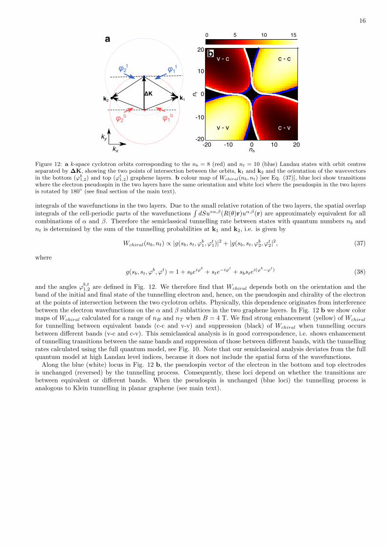
16
a
kx
ky
ΔKk1k2
φ2t
φ1t
φ2b φ1
b
nt
20
0
-10
-20
b10
20100-20nb
-10
0 15
c - c
v - v c - v
v - c
5 10
Figure 12: a k-space cyclotron orbits corresponding to the nb = 8 (red) and nt = 10 (blue) Landau states with orbit centresseparated by ∆K, showing the two points of intersection between the orbits, k1 and k2 and the orientation of the wavevectorsin the bottom (ϕb
1,2) and top (ϕt1,2) graphene layers. b colour map of Wchiral(nb, nt) [see Eq. (37)], blue loci show transitions
where the electron pseudospin in the two layers have the same orientation and white loci where the pseudospin in the two layersis rotated by 180◦ (see final section of the main text).
integrals of the wavefunctions in the two layers. Due to the small relative rotation of the two layers, the spatial overlapintegrals of the cell-periodic parts of the wavefunctions
∫dSu∗α,β(R(θ)r)uα,β(r) are approximately equivalent for all
combinations of α and β. Therefore the semiclassical tunnelling rate between states with quantum numbers nb andnt is determined by the sum of the tunnelling probabilities at k1 and k2, i.e. is given by
Wchiral(nb, nt) ∝ |g(sb, st, ϕb1, ϕ
t1)|2 + |g(sb, st, ϕ
b2, ϕ
t2|2, (37)
where
g(sb, st, ϕb, ϕt) = 1 + sbe
iϕb
+ ste−iϕt
+ sbstei(ϕb−ϕt) (38)
and the angles ϕb,t1,2 are defined in Fig. 12. We therefore find that Wchiral depends both on the orientation and theband of the initial and final state of the tunnelling electron and, hence, on the pseudospin and chirality of the electronat the points of intersection between the two cyclotron orbits. Physically, this dependence originates from interferencebetween the electron wavefunctions on the α and β sublattices in the two graphene layers. In Fig. 12 b we show colormaps of Wchiral calculated for a range of nB and nT when B = 4 T. We find strong enhancement (yellow) of Wchiral
for tunnelling between equivalent bands (c-c and v-v) and suppression (black) of Wchiral when tunnelling occursbetween different bands (v-c and c-v). This semiclassical analysis is in good correspondence, i.e. shows enhancementof tunnelling transitions between the same bands and suppression of those between different bands, with the tunnellingrates calculated using the full quantum model, see Fig. 10. Note that our semiclassical analysis deviates from the fullquantum model at high Landau level indices, because it does not include the spatial form of the wavefunctions.
Along the blue (white) locus in Fig. 12 b, the pseudospin vector of the electron in the bottom and top electrodesis unchanged (reversed) by the tunnelling process. Consequently, these loci depend on whether the transitions arebetween equivalent or different bands. When the pseudospin is unchanged (blue loci) the tunnelling process isanalogous to Klein tunnelling in planar graphene (see main text).
17
[1] Liu, Y., Bian, G., Miller, T. and Chiang, T.-C. Visualizing Electronic Chirality and Berry Phases in Graphene SystemsUsing Photoemission with Circularly Polarized Light. Phys. Rev. Lett. 107, 166803 (2011).
[2] Young, A. F. and Kim, P. Quantum interference and Klein tunnelling in graphene heterojunctions. Nat. Phys. 5, 222 - 226(2009)
[3] Katsnelson, M. I., Novoselov, K. S. and Geim A. K. Chiral tunnelling and the Klein paradox in graphene. Nat. Phys. 2,620-625 (2006).
[4] Geim, A. K. and Grigorieva, I. V. Van der Waals heterostructures. Nature 499, 419-425, (2013).[5] Britnell, L. et al. Field-effect tunneling transistor based on vertical graphene heterostructures. Science 335, 947-950, (2012).[6] Britnell, L. et al. Resonant tunnelling and negative differential conductance in graphene transistors. Nat. Commun. 4,
1794, (2013).[7] Fallahazad, B. et al. Gate-Tunable Resonant Tunneling in Double Bilayer Graphene Heterostructures. Nano Lett. 15, 1
(2015).[8] Mishchenko, A. et al. Twist-controlled resonant tunnelling in graphene / boron nitride / graphene heterostructures. Nature
Nanotech. 9, 808813 (2014).[9] Feenstra, R. M, Jena, D. and Gu, G. Single-particle tunneling in doped graphene-insulator-graphene junctions. J. Appl.
Phys. 111, 043711 (2012).[10] Zhao, P., Feenstra, R. M., Gu, G. and Jena, D. SymFET: A Proposed Symmetric Graphene Tunneling Field-Effect
Transistor. IEEE Trans. Electron Devices 60, 951957 (2013).[11] Vasko, F. T. Resonant and nondissipative tunneling in independently contacted graphene structures. Phys. Rev. B 87,
075424 (2013).[12] Brey, L. Coherent tunneling and negative differential conductivity in a graphene/h-BN/graphene heterostructure. Phys.
Rev. Appl. 2, 014003 (2014).[13] Eisenstein, J. P., Pfeiffer, L. N. and West K. W. Coulomb barrier to tunneling between parallel two-dimensional electron
systems. Phys. Rev. Lett 69, 3804 (1992).[14] Leadbeater, M. L., Sheard, F. W. and Eaves, L. Inter-Landau-level transitions of resonantly tunnelling electrons in tilted
magnetic fields. Semicond. Sci. Technol. 6, 1021 (1991).[15] Lee, G. H. et al. Electron tunneling through atomically flat and ultrathin hexagonal boron nitride. Appl. Phys. Lett. 99,
243114 (2011).[16] Lopes dos Santos, J. M. B., Peres, N. M. R. and Castro Neto, A. H. Graphene Bilayer with a Twist: Electronic Structure.
Phys. Rev. Lett. 99, 256802 (2007).[17] Mele, E. J. Commensuration and interlayer coherence in twisted bilayer graphene. Phys. Rev. B 81, 161405 (2010).[18] Bistritzer, R. and MacDonald, A. H. Transport between twisted graphene layers. Phys. Rev. B 81, 245412 (2010).[19] Bistritzer, R. and MacDonald, A. H. Moire bands in twisted double-layer graphene. Proc. Natl. Acad. Sci. U. S. A. 108,
122337 (2011).[20] Li, G., Luican, A. and Andrei, E. Y. Scanning Tunneling Spectroscopy of Graphene on Graphite. Phys. Rev. Lett., 102,
176804 (2009).[21] Ponomarenko, L. A. et. al Density of States and Zero Landau Level Probed through Capacitance of Graphene. Phys. Rev.
Lett. 105, 136801 (2010).[22] Shon, N. and Ando, T. Quantum Transport in Two-Dimensional Graphite System. J. Phys. Soc. Jpn. 67, 2421 (1998).[23] Zheng, Y. and Ando, T. Hall conductivity of a two-dimensional graphite system. Phys. Rev. B 65, 245420 (2002).[24] Li, G., Luican-Mayer, A., Abanin, D., Levitov, L. and Andrei, E. Y. Evolution of Landau levels into edge states in graphene.
Nat. Commun. 4, 1744 (2013).[25] Luican-Mayer, A. et al. Screening Charged Impurities and Lifting the Orbital Degeneracy in Graphene by Populating
Landau Levels. Phys. Rev. Lett. 112, 036804 (2013).[26] Zhang, Y, Tan, Y. W., Stormer, H. L., and Kim P, Experimental observation of the quantum Hall effect and Berry’s phase
in graphene. Nature 438, 201-204 (2005).[27] Fu, Y.-S. et. al Imaging the two-component nature of Dirac-Landau levels in the topological surface state of Bi2Se3. Nat.
Phys. 10 815-819 (2014).[28] Miller, D. L. et. al Real-space mapping of magnetically quantized graphene states. Nat. Phys. 6 811-817 (2010).[29] Zhang, Y. et. al Landau-Level Splitting in Graphene in High Magnetic Fields. Phys. Rev. Lett., 96, 136806 (2006).[30] Pratley, L. and Zulicke, U. Magnetotunneling spectroscopy of chiral two-dimensional electron systems. Phys. Rev. B 88,
245412 (2013).[31] Pratley, L. and Zulicke, U. Valley filter from magneto-tunneling between single and bi-layer graphene. Appl. Phys. Lett.
104 082401 (2014).[32] Pershoguba, S. S., Abergel, D. S. L., Yakovenko, V. M., and Balatsky, A. V. Effects of a tilted magnetic field in a Dirac
double layer. Phys. Rev. B 91 085418 (2015)[33] Drallos, P. J. and Wadehra, J. M. Exact evaluation and recursion relations of two-center harmonic oscillator matrix
elements. J. Chem. Phys. 85, 6524 (1986).