Embed Size (px)
Citation preview
1
RFDESIGNFORHIGHSYSTEMINTEGRATION
Theperformedresearchhasfollowedtheplanoutlinedintheprojectproposal.TheonlyexceptionhasbeenTask1.6thatintheproposalwasscheduledtostartat the end of the first year of the project (month 12) and was, instead,immediately startedat timezero, favoredby theavailabilityof aPh.D. studentworkingonaZig‐Betransceiver.Thechoiceactuallyenhancedtheorganizationof the overall FIRB activity facilitating the implementation of Activity 13 thatrequirescooperationbetweenthevariousresearchunits.
Theunifying themebetweenvarious tasks isadeeplyscaledCMOS technologyused forextending the levelof integrationofwireless communicationsystems.AllRFandanalogbasebandcriticalIP’sforevermore‐complicatedSystemsonaChip(SOC’s)mustbedesigned.
Task1.4focusesonthetransmitportionofhighbitrateterminalsforWLANandWWAN. The main objective is optimum performance in terms of area bill ofmaterialandpowerconsumption.Thetaskstudiesbotharchitectureandcircuitimplementations of the transmit portion of transceiver and power amplifier.Morespecifically,westudiedall‐digitalPLLsforanalyzingtheirpotentialuseindigitally intensivetransmitters.AnewarchitectureforahighresolutionDigitalControlled Oscillator is under study and its circuit prototypewill be designedandfabricatednextyear.InadditionaclassA/BpoweramplifierforaDoherthyarchitecturehasbeendesignedandtested.
Task1.5focusesonRFbody‐netandRFIDandmorespecificallyontheZig‐Beestandard.Evenforthiscasetheobjectiveisminimizingcostintermsofareabillof material and power consumption at a relatively small date rate. The taskrealizedandtestedtwoversionsofcompletereceiverwithsignificantreductiononareaandpower.Thetransmitter,nowunderinvestigationwillbeprototypednextyear.
Task 1.6 is for acquiring the basic technology know‐how required to properlyexploit most deeply scaled technologies and cope with critical limitationaffectinganalogandRFapplicationlike,forexample,theincreased1/fnoise.
Task1.4:AdvancedRFDesign
Thirdgenerationcellularcommunicationsstandards,suchasUMTS,useefficientmodulationschemes.Sincethemodulatedsignalchangesphaseandamplitude,inordertopreservetheinformationonamplitudevariation,signaltransmissionmustbedonewithlinearPowerAmplifiers(PAs)orbylinearizationtechniquesof non‐linear PAs. The advantage of intrinsic linearity of the former approachcostsapooraverageefficiencytypicaloflinearPAs.Thelatterenablestheuseofefficientnon‐linearPAsbutobtaininggoodlinearitywithcorrectingschemesisdifficult.
2
Since battery duration is the main concern in portable wireless devices,transmitter efficiency is very important. Convenient efficiency enhancementtechniques maximize the efficiency compared to standard linear PA whilemaintainingthelinearityproperties.ThemostinterestingmethodistheDohertyarchitecturethatincreasestheaverageefficiencyofaPAworkinginclassAB.
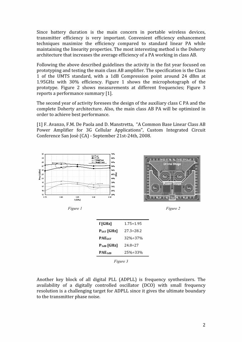
FollowingtheabovedescribedguidelinestheactivityinthefistyearfocusedonprototypingandtestingthemainclassABamplifier.ThespecificationistheClass1 of the UMTS standard, with a 1dB Compression point around 24 dBm at1.95GHz with 30% efficiency. Figure 1 shows the microphotograph of theprototype. Figure 2 shows measurements at different frequencies; Figure 3reportsaperformancesummary[1].
ThesecondyearofactivityforeseesthedesignoftheauxiliaryclassCPAandthecompleteDohertyarchitecture.Also, themainclassABPAwillbeoptimized inordertoachievebestperformance.
[1]F.Avanzo,F.M.DePaolaandD.Manstretta,“ACommonBaseLinearClassABPower Amplifier for 3G Cellular Applications”, Custom Integrated CircuitConferenceSanJosè(CA)‐September21st‐24th,2008.
Figure 1 Figure 2
Figure 3
Another key block of all digital PLL (ADPLL) is frequency synthesizers. Theavailability of a digitally controlled oscillator (DCO) with small frequencyresolutionisachallengingtargetforADPLLsinceitgivestheultimateboundarytothetransmitterphasenoise.
f[GHz] 1.75÷1.95
PSAT[GHz] 27.3÷28.2
PAESAT 32%÷37%
P1dB[GHz] 24.8÷27
PAE1dB 25%÷33%

3
ThefirstyearactivitydesignedaDCOwithverytinyfrequencyresolution(lessthan 40 Hz). The result was achieved by the use of an active “gyrator” whichshrinks the capacitive load seenby the tankandobtainsanequivalentunitarycapacitanceof0.3aF.
The DCO meets phase noise specifications of the GSM standard with powerconsumptionof13.2mW.TheF.o.Mis‐195dBc/Hz.OthersimulationresultsarereportedinTableI.
Result
Oscillator’scentralfrequency 3.6GHz
Tuningrange 800MHz
Frequencyresolution 30÷40Hz
PhaseNoise@400kHz ‐128dBc/Hz
PhaseNoise@20‐80MHz ‐163dBc/Hz
Powerconsumption 13.2mW
F.o.M ‐195dBc/Hz
Table I
We are moving to the layout and fabrication of a test chip to experimentallyvalidatetheproposedtechnique.
Task1.5:RFbodynetandRFID
Short range, low data rate systems are important for wireless networkingresearch.Emergingapplicationsarebuildingautomation,industrialcontrolandpersonal health care. The main features of terminals must be low power, toincreasebatterylife,andlowcosttofavorwideuse.ThemostusedstandardistheZigBee,whichallowssolutionssuitableforcommercialneeds.Followingthistrend this project aims at realizing an integrated transceivers with very lowpowerconsumptionoperatingintheIMSband(2.4GHz).
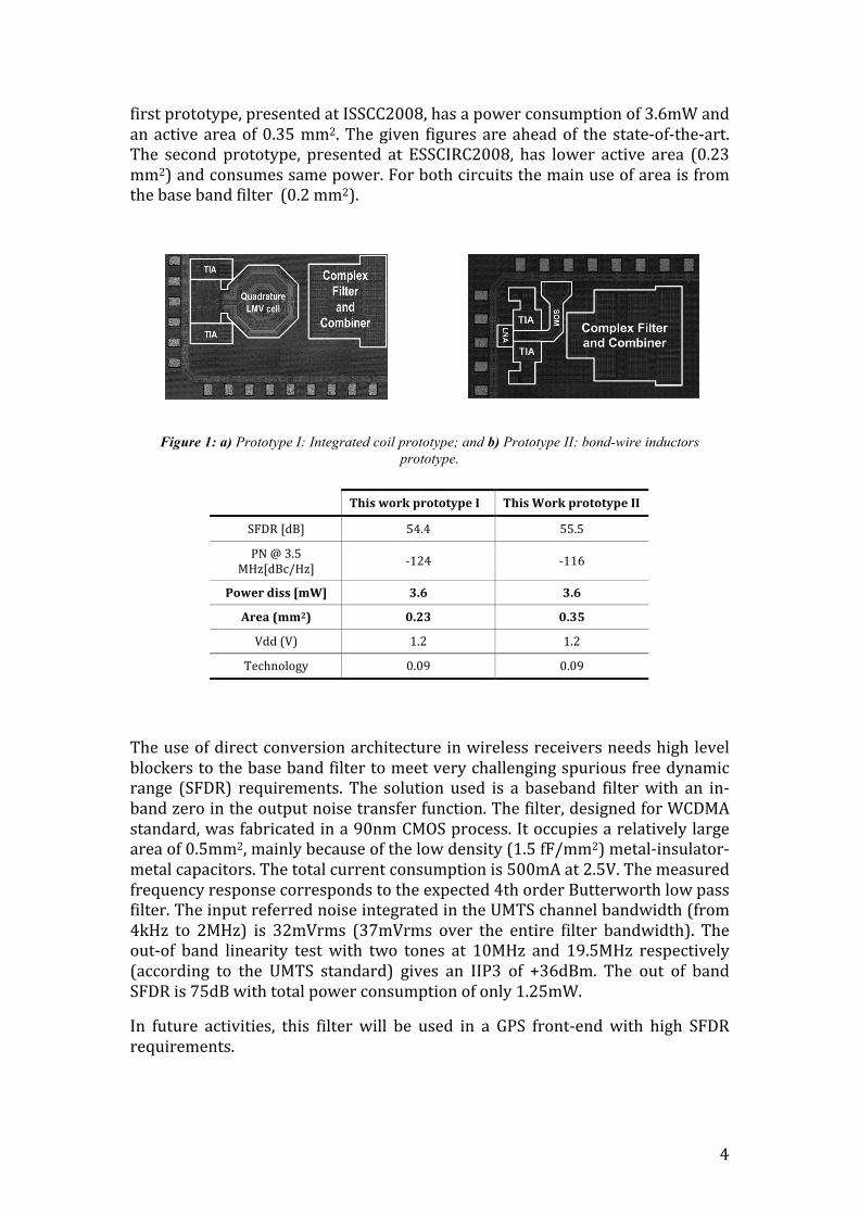
Thefirstyearactivityconcentratedonthereceiverpath.TwolowIFarchitectureprototypeshavebeen integrated.Theyexploita techniquethatreusingcurrentreducespower.Theschemeincludesabasebandvariablegaincomplexfilterforchannelselection.ThefirstprototypeemploysanI‐QLMV.Itstacksalownoiseamplifieranda selfoscillatingmixerbetweenGNDandVDD, thussharingbiascurrentanddevices.The IandQpathsshare theLC tankreducingbothpowerconsumptionandsiliconareaatthecostoflimitedamplitudeandphaseerrorsinthepaths.Themethodoftanksharingisalsousedinthesecondprototype.High‐Q bond‐wire inductors in a double‐input‐double‐output SOMminimize area. Adetailedstudyof theSOMconversiongainandtheamplitude/phaseerrorshasoptimizedtheLCtankconfigurationandhasminimizedlossandmismatch.The
4
firstprototype,presentedatISSCC2008,hasapowerconsumptionof3.6mWandanactiveareaof0.35mm2.Thegiven figuresareaheadof the state‐of‐the‐art.The second prototype, presented at ESSCIRC2008, has lower active area (0.23mm2)andconsumessamepower.Forbothcircuitsthemainuseofareaisfromthebasebandfilter(0.2mm2).
Figure 1: a) Prototype I: Integrated coil prototype; and b) Prototype II: bond-wire inductors
prototype.
Theuseofdirectconversionarchitectureinwirelessreceiversneedshighlevelblockerstothebasebandfiltertomeetverychallengingspuriousfreedynamicrange (SFDR) requirements. The solution used is a baseband filterwith an in‐bandzerointheoutputnoisetransferfunction.Thefilter,designedforWCDMAstandard,wasfabricatedina90nmCMOSprocess.Itoccupiesarelativelylargeareaof0.5mm2,mainlybecauseofthelowdensity(1.5fF/mm2)metal‐insulator‐metalcapacitors.Thetotalcurrentconsumptionis500mAat2.5V.Themeasuredfrequencyresponsecorrespondstotheexpected4thorderButterworthlowpassfilter.TheinputreferrednoiseintegratedintheUMTSchannelbandwidth(from4kHz to 2MHz) is 32mVrms (37mVrms over the entire filter bandwidth). Theout‐of band linearity test with two tones at 10MHz and 19.5MHz respectively(according to the UMTS standard) gives an IIP3 of +36dBm. The out of bandSFDRis75dBwithtotalpowerconsumptionofonly1.25mW.
In future activities, this filter will be used in a GPS front‐endwith high SFDRrequirements.
ThisworkprototypeI ThisWorkprototypeII
SFDR[dB] 54.4 55.5
[email protected][dBc/Hz] ‐124 ‐116
Powerdiss[mW] 3.6 3.6
Area(mm2) 0.23 0.35
Vdd(V) 1.2 1.2
Technology 0.09 0.09
5
Figure 2: a) Results; and b) Chip micrograph.
Publishedresults
A. Liscidini, M. Tedeschi, R. Castello, “A 2.4 GHz 3.6mW 0.35mm2 QuadratureFront‐EndRXforZigBeeandWPANApplications”IEEEISSCCDig.Tech.Papers,Feb.2008,pp.370‐371.
M.Tedeschi,A.Liscidini,R.Castello,“A0.23mm2freecoilZigBeeReceiverbasedon a bond‐wire self‐oscillating mixer”, IEEE ESSCIRC Dig. Tech. Papers, Sept.2008,pp.430‐433.
A.Liscidini,A.Pirola,R.Castello,“A1.25mW75dBSFDRContinuousTimeFilterwithin‐bandnoisereduction”,IEEEISSCC,Feb.2009.
Task1.6:LownoiseAnalogDesign
The first year of research activity focused on two main subjects: thecharacterizationof130nmand90nmCMOSprocesses, inparticular from thestandpointofthegateleakagecurrentnoiseandthestudyofradiationhardnessproperties of CMOS monolithic active pixel sensors, fabricated in a 130 nmprocess.For theanalysisvarious teststructureshavebeenexposedtophotonsfromagamma‐raysource.
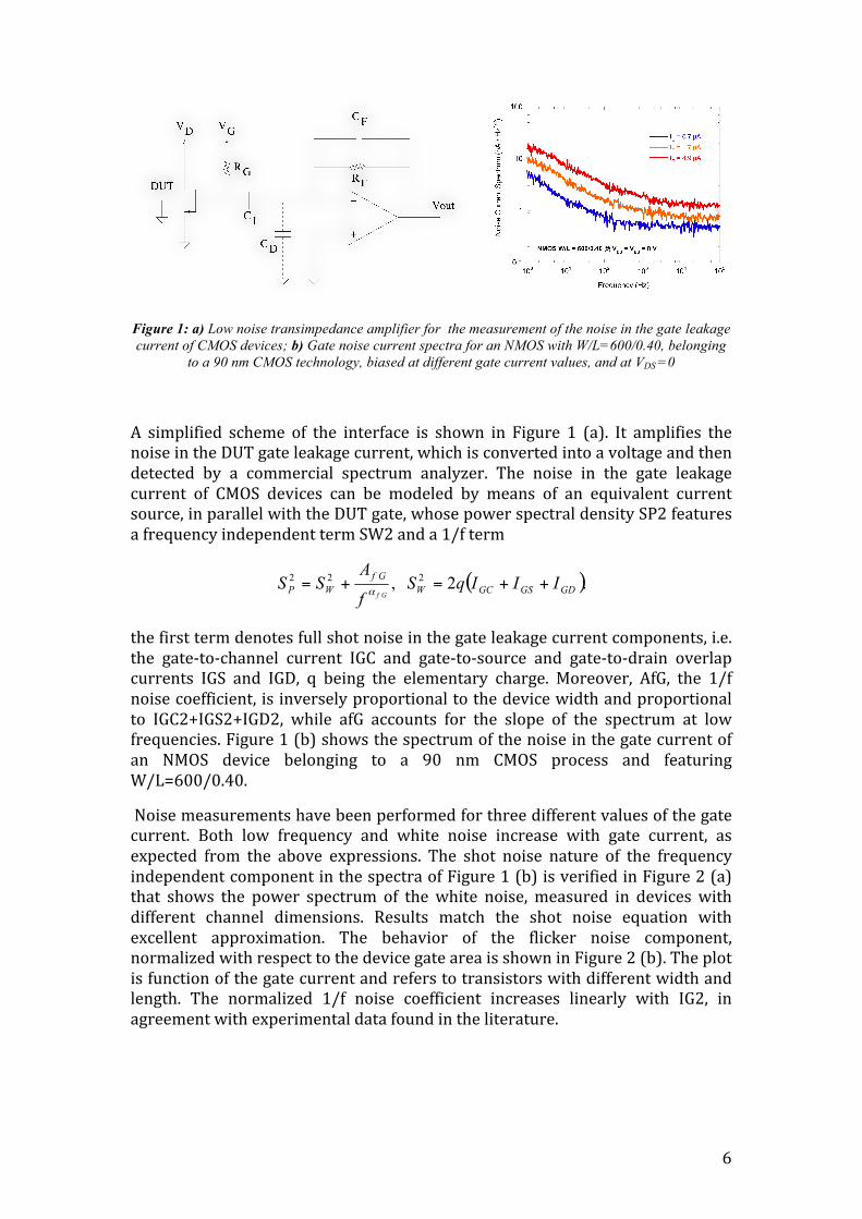
AsignificantnumberofNMOSandPMOSdeviceswithdifferentgatelengthandwidthunderdifferentbiasconditionsenablesthestudyofgatecurrentnoiseindeepsubmicronCMOS.Thepowerspectraldensityofthenoisewasmeasuredinthe frequency range 1 Hz 100 kHz, therefore including low frequency (1/f orLorentzian) white and shot noise contributions. Noise measurements wereperformedbyanad‐hocinterfacemadebyalownoisetransimpedanceamplifierandthenetworkforbiasingtheDUT(deviceundertest).
6
Figure 1: a) Low noise transimpedance amplifier for the measurement of the noise in the gate leakage current of CMOS devices; b) Gate noise current spectra for an NMOS with W/L=600/0.40, belonging
to a 90 nm CMOS technology, biased at different gate current values, and at VDS =0
A simplified scheme of the interface is shown in Figure 1 (a). It amplifies thenoiseintheDUTgateleakagecurrent,whichisconvertedintoavoltageandthendetected by a commercial spectrum analyzer. The noise in the gate leakagecurrent of CMOS devices can be modeled by means of an equivalent currentsource,inparallelwiththeDUTgate,whosepowerspectraldensitySP2featuresafrequencyindependenttermSW2anda1/fterm
thefirsttermdenotesfullshotnoiseinthegateleakagecurrentcomponents,i.e.the gate‐to‐channel current IGC and gate‐to‐source and gate‐to‐drain overlapcurrents IGS and IGD, q being the elementary charge. Moreover, AfG, the 1/fnoisecoefficient,isinverselyproportionaltothedevicewidthandproportionalto IGC2+IGS2+IGD2, while afG accounts for the slope of the spectrum at lowfrequencies.Figure1(b)showsthespectrumofthenoiseinthegatecurrentofan NMOS device belonging to a 90 nm CMOS process and featuringW/L=600/0.40.
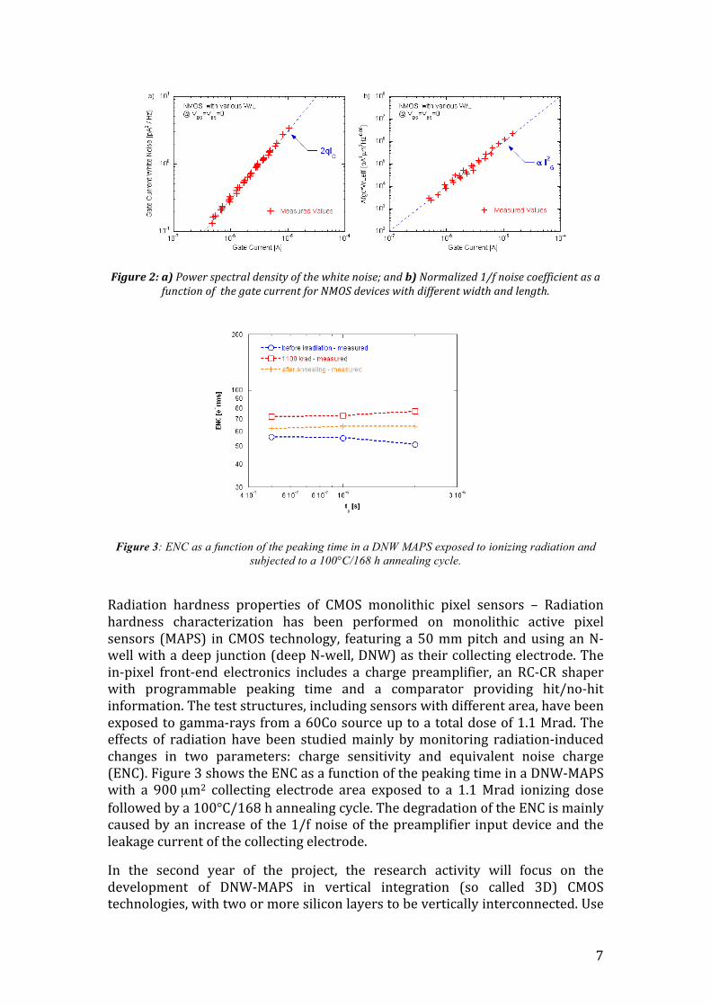
Noisemeasurementshavebeenperformedforthreedifferentvaluesofthegatecurrent. Both low frequency and white noise increase with gate current, asexpected from the above expressions. The shot noise nature of the frequencyindependentcomponentinthespectraofFigure1(b)isverifiedinFigure2(a)that shows the power spectrum of thewhite noise,measured in deviceswithdifferent channel dimensions. Results match the shot noise equation withexcellent approximation. The behavior of the flicker noise component,normalizedwithrespecttothedevicegateareaisshowninFigure2(b).Theplotisfunctionofthegatecurrentandreferstotransistorswithdifferentwidthandlength. The normalized 1/f noise coefficient increases linearly with IG2, inagreementwithexperimentaldatafoundintheliterature.
7
Figure2:a)Powerspectraldensityofthewhitenoise;andb)Normalized1/fnoisecoefficientasa
functionofthegatecurrentforNMOSdeviceswithdifferentwidthandlength.
Figure 3: ENC as a function of the peaking time in a DNW MAPS exposed to ionizing radiation and subjected to a 100°C/168 h annealing cycle.
Radiation hardness properties of CMOS monolithic pixel sensors – Radiationhardness characterization has been performed on monolithic active pixelsensors (MAPS) inCMOS technology, featuringa50mmpitchandusinganN‐wellwithadeepjunction(deepN‐well,DNW)astheircollectingelectrode.Thein‐pixel front‐end electronics includes a charge preamplifier, an RC‐CR shaperwith programmable peaking time and a comparator providing hit/no‐hitinformation.Theteststructures,includingsensorswithdifferentarea,havebeenexposedtogamma‐raysfroma60Cosourceuptoatotaldoseof1.1Mrad.Theeffects of radiation have been studiedmainly bymonitoring radiation‐inducedchanges in two parameters: charge sensitivity and equivalent noise charge(ENC).Figure3showstheENCasafunctionofthepeakingtimeinaDNW‐MAPSwith a 900µm2 collecting electrode area exposed to a 1.1Mrad ionizing dosefollowedbya100°C/168hannealingcycle.ThedegradationoftheENCismainlycausedbyan increaseof the1/fnoiseof thepreamplifier inputdeviceandtheleakagecurrentofthecollectingelectrode.
In the second year of the project, the research activity will focus on thedevelopment of DNW‐MAPS in vertical integration (so called 3D) CMOStechnologies,withtwoormoresiliconlayerstobeverticallyinterconnected.Use
8
of these fabrication techniquesmayhelp increase the functionaldensityof theMAPSfront‐endcircuitsand improvetheirpropertiesby including in thepixel,on a different layer form the sensor, more complex digital blocks forsparsificationand/orzerosuppression.