Embed Size (px)
Citation preview
光伏科学与技术国家重点实验室State Key Laboratory of PV Science & Technology
Annual Report 2016State Key Laboratory of PV Science & Technology
PVSTChangzhou Trina Solar Energy Co., Ltd
Scientific Achievement Highlights, 2016
Address
No. 2 Trina Road, Trina PV Park
New District, Changzhou, Jiangsu, P.R. China
Fax +86 519 81587444
www.sklpvst.com
Research Achievements◆ Record cell efficiency of 23.5% for 156*156mm2 IBC Si
solar cell
◆ Record cell efficiency of 19.86% for P-type Honey Plus
polycrystalline Si solar cell
◆ Record cell efficiency of 22.61% for P-type monocrys-
talline Si PERC solar cell
◆ Cell efficiency of 22.40% (tested in laboratory) for
6-inch bifacial N-type PERT cell
◆ Cell efficiency of 21.4% for 6-inch bifacial N-type PERT
cell in pilot production
Awards◆ Dr Pierre Verlinden was honored with 2016 Willian R. Cherry
Award in 43rd IEEE PVSC
◆ DUOMAX dual glass solar module was the first to pass the
latest accreditation criteria of ‘Top Runner’Dual Glass
Solar Module Technical Specifications
◆ Osaka Sangyo University’s solar cell, equipped with Trina
Solar’s IBC solar modules, won the championship of ‘Dre-
am Group’ in the 2016 FIA Solar Car Race
◆ Trina Solar was among the first batch in China to pass NIM
(National Institute of Methology) module power measuring
uncertainity assessment certification
◆ Invention patent (No. of ZL201210141633.5) -13th Patent
Golden Award of Changzhou and 18th China Patent Excell-
ence Award for interdigitated back contact solar cell fabri-
cation method
◆ Trina Solar received the Second Prize of 2016 National Fed-
eration of Industry and Commerce Sci-Tech Advance Award
Scientific Papers & Patents & Standards
◆ Scientific papers: 36 papers published in scientific
journals and key international PV conferences
◆ Patents: 97 patents approved including 38 invention
patents
◆ Published Standards: industrial standards of speci-
fication for ultra-thin glasses used for photovoltaic
modules (SJ/T 11571-2016), graphical symbols for
solar photovoltaic energy systems (SJ/T 10460
-2016)
光伏科学与技术国家重点实验室State Key Laboratory of PV Science & Technology
Annual Report in 2016State Key Laboratory of PV Science & Technology
PVSTChangzhou Trina Solar Energy Co., Ltd
Scientific Achivement Highlights, 2016
Research Achievements◆ Record cell efficiency of 23.5% for 156*156mm2 IBC Si
solar cell
◆ Record cell efficiency of 19.86% for P-type Honey Plus
polycrystalline Si solar cell
◆ Record cell efficiency of 22.61% for P-type monocrystal-
line Si PERC solar cell
◆ Cell efficiency of 22.40% (tested in laboratory) for 6-inch
bifacial N-type PERT cell
◆ Cell efficiency of 21.4% for 6-inch bifacial N-type PERT
cell in pilot production
Scientific Papers & Patents &
Standardsdards◆ Scientific papers: 36 papers published in scientific
journals and key international PV conferences
◆ Patents: 97 patents approved including 38 invention
patens
◆ Published Standards: industrial standards of
Specification for ultra-thin glasses used for
photovoltaic modules (SJ/T 11571-2016), Graphical
symbols for solar photovoltaic energy systems (SJ/T
10460-2016)
Address
No. 2 Trina Road, Trina PV Park
New District, Changzhou, Jiangsu, P.R. China
Fax +86 519 81587444
www.sklpvst.com
Awards◆ Dr Pierre Verlinden was honored with 2016 Willian R. Cherry
Award in 43rd IEEE PVSC.
◆ Doumax dual glass solar module was the first to pass the
latest accreditation criteria of ‘Top Runner’ Dual Glass
Solar Module Technical Specifications.
◆ Osaka Sangyo University’s solar cell, equipped with Trina
Solar’s IBC solar modules, won the championship of
‘Dream Group’ in the 2016 FIA Solar Car Race.
◆ Trina Solar was among the first batch in China to pass NIM
(National Institute of Methology) module power measuring
uncertainity assessment certification.
◆ Invention patent (No. of ZL201210141633.5) -13th Patent
Golden Award of Changzhou and 8th China Patent
Excellence Award for interdigitated back contact solar cell
fabrication method
◆ Trina Solar received the Second Prize of 2016 National
Federation of Industry and Commerce Sci-Tech Advance
Award.
◆ Benefit mankind with solar energy!
VISION
MISSION
◆ Reduce cost by efficiency improvement ; Attain development through technical innovation.◆ Bring solar energy to every household.
1IRENA (2016), ‘Letting in the light: How solar photovoltaics will revolutionise the electricity system'.2Ibid.
Chief Scientist and Vice-President of Trina Solar and the Vice -Chair of the State Key Laboratory, who has been selected, in June, as the 2016 William R. Cherry award recipient for his dedication over the past three decades at the past three de-cades at the forefront of PV technology research and com-mercialisation, and his overall leadership at key R&D organ-isations.
As leaders of the SKL of PVST, Dr Pierre Verlinden and I feel very honoured and thank all the teams of PV research-ers and scientists who have enhanced Trinasolar’s key PV technologies through innovation that have resulted in sever-al world-record cell and module efficiencies in recent years. We would also like to take this opportunity to congratulate two of our great PV researchers, Dr Qiangzhong Zhu and Dr Weiyuan Duan, who have received Excellent Scientific Paper Award at the 16th China Photovoltaic Technical Conference in October.
The SKL of PVST was invited to produce high-efficiency IBC solar cells again for the Osaka Sangyo University (OSU) Solar Car, following the successful collaboration last year. With improved processing optimisation, the average efficien-cy of the cells provided this year was 23%, 0.5%abs higher than that of last years. The OSU Solar Car won the “Dream Class” category this year where the racing car was required to large-ly depend on the power generation capacity of the solar cells rather than the battery's , and required the team to carefully manage the energy consumption during the 5-hour race.
Our successful collaboration with solar racing cars in-stilled in us a vision of incorporating high-efficiency PV prod-ucts into commercial cars and this year we set up a mobile PV team to foster technology collaboration with the automo-bile industry. Our mobile PV team is working with premium automobile companies in Japan and Europe whereby Trina Solar provides solar cells for car roofs of their electrical vehi-cles to power the internal temperature regulation manage-ment system. Similar contracts have also been successfully negotiated for the public transport in India.
Within the four walls of our Laboratory, a great progress in ingot and wafer research has been achieved. 1) High qual-ity multicrystalline wafer labelled as T1 (Trina 1#) reached the state-of-the-art wafer level in the market and was em-ployed in the high-efficiency cell production line; 2) Diamond wire slicing technique for the multicrystalline ingot was ex-plored successfully. The total yield was up 96% with remark-able cost reduction; 3) The monocrystalline ingot research has also been rewarding - the pulling speed reached up to 1.25 mm/min at 53 kW power. We believe that the high quality
Driven by a strong business case and falling costs, pho-tovoltaic energy has progressed remarkably over the past decade, and has become the preferred power source for many countries, poising to revolutionise the electrical system in countries around the world. On a global level, the weighted average levelised cost of electricity (LCOE) for utili-ty-scale solar PV has reached USD 0.13/kWh in 2015 and is forecasted to fall by 59% by 2025 with the right policies1. The upfront cost of building a solar PV plant is now close to or even lower than that of a conventional power generation2. While the solar PV offers enormous opportunities, it currently provides less than 2% of global electricity today and a higher level of penetration, especially beyond 20% grid integration, will only come about with a host of new activities such as de-mand-side management, electrification of the transport and integration with buildings etc. In order for these new activi-ties to foster, efforts to increase PV efficiencies and lower costs should be encouraged and pursued ‒ PV efficiencies over 40% will allow for radically different uses such as inte-gration into electric vehicles, and combined with lower costs, will open up incredible new opportunities for solar PV de-ployment in urban environments. Supported by our core mission - i.e. to develop a cheaper photovoltaic solar energy to benefit mankind by developing leading PV techniques and products that improve the product efficiency and reduce the system cost ‒ our researchers and scientists are working to-wards such future.
2016 has been a rewarding year for the State Key Labo-ratory of Photovoltaic Science and Technology (SKL of PVST)- numerous world records have been achieved; new mobile PV team has been established in response to the special and new market demand; and academic collaborations and ex-changes with PV experts around the world have continued to flourish.
This year, we are very honoured to welcome Professor Martin Green as our academic committee member. Professor Martin Green, often known as the “Father of Photovoltaics”, has over 40 years of PV research career and made distin-guished contributions to both commercial and academic fields of photovoltaics. He has set numerous world records for silicon based solar cells and pioneered the field of “third generation” photovoltaics which investigates advanced, high-efficiency photovoltaic device concepts in order to re-alise the fundamental limits of solar cell efficiency. We look forward to collaborating on the high-efficiency PV device pro-grammes at SKL of PVST.
We would like to congratulate Dr Pierre Verlinden, the
wafer is not only beneficial to the cell efficiency and module power output, but also to the module reliability.
In April this year, our high-efficiency solar cell team set a new world record of 23.5% with an IBC structure on a large-area (156x156mm2) n-type mono-crystalline silicon wafer. The solar cell was fabricated entirely with low-cost indus-trial screen-printed processes. This record not only broke the previous record of 22.94% for the same type of solar cell that was also set by the Laboratory in May, 2014, but follows the previous record of a 24.4% small-area (2x2cm2) labora-tory IBC solar cell developed just two years prior, in collabo-ration with the Australian National University (ANU). To the best of our knowledge, this was the first time that a mono-crystalline silicon IBC solar cell on a large-area (6-inch) wafer reached a total-area efficiency of 23.5%. In July, the aver-age output of a 60-cell p-type mono-crystalline module con-structed with standard industrial production materials and processes reached 300W by assembling PERC cells with an average cell efficiency of 21.1%. The said 21.1% average ef-ficiency was a major efficiency improvement breakthrough for the industrial monocrystalline PERC cell and demonstrat-ed the Laboratory's technological strength in transferring laboratory technology to mass production. Shortly thereaf-ter in the same month, the Laboratory further solidified the leading position in cutting-edge PV technology for the mass production of high-efficiency PV products by achieving an average efficiency of 20.16% for its p-type multi-crystalline PERC cells produced with industrial processes. The cell was built with advanced PERC technology and materials devel-oped at the Laboratory including high-performance p-type Trina-1 wafers. In October, the Laboratory set another world record for a p-type multi-crystalline PERC module aperture ef-ficiency. Consisting of 120 pieces of “half-cell” (156x78mm2), the module was independently developed with high-perfor-mance wafers and advanced in-house module technologies
orewordand its aperture efficiency reached 19.86%. The new record presents an increase of more than 0.7%abs, or approximate-ly 3.8% higher than the previous aperture efficiency record of 19.14% announced a year and half earlier. We are very excited about this achievement as it demonstrates the huge potential for the future multi-crystalline p-type silicon research. In De-cember, the self-developed P-type PERC solar cell has created another world record with the conversion efficiency reaching up to 22.61%, which is the highest efficiency achieved for the large-area industrialized P-type mono-crystalline PERC solar cells.
Our module team continued commendable work this year by transferring high-efficiency laboratory module tech-nologies to the mass production. The first climate-specific ad-vanced Duomax double glass module, Sahara, is now mass-production ready as well as the 120-“half-cell” p-type mono-crystalline module, Splitmax. Sahara, as the name suggests, has been developed for dry and sandy regions that experi-ence cycles of extremely high and low temperatures. First in its series, the linear degradation of Sahara module’s maxi-mum power output is 0.12% (annual) lower than that of the conventional double glass module. The continued improve-ment effort on the Duomax double glass was recognised in July when it became the first PV module to have obtained the accreditation as part of the Chinese government led ‘Top Runner’3 programme. Meanwhile, we have successfully de-veloped Splitmax module product, which is composed of 120 P-type mono-crystalline half-cells.
In the area of patents, Trina Solar still holds the highest number of invention patents amongst the Chinese PV manu-facturers. This year alone, 106 patents have been filed and 97 patents have been approved. Of the 106 patents, 51 patents are invention patents highlighting the Laboratory’s lead on innovation. Cumulatively, as of December 31, 2016, 1317 pat-ents have been filed by Trina Solar and of those, 597 are in-vention patents. In the area of standards, the Laboratory has participated in 64 standards in total as of December 2016. 45 standards have been published including 10 guided stan-dards. 14 standards under research include 1 IEC standard, 4 SEMI standards, 5 national standards and 4 industry stan-dards.
As we reflect on the many achievements in 2016, I would like to thank all the dedicated and hard-working teams and stakeholders. Thank you for your commitment to building a world where PV plays a vital role in benefitting mankind.
Dr. Zhiqiang Feng Vice President of Changzhou Trina Solar Energy Co., LtdDirector of the State Key Laboratory of Photovoltaic Sci-
ence & TechnologyDecember 31, 2016
3 As the installation rush took place in the first half of 2016, Chinese government established module efficiency requirements for domestic projects and encouraged wider adoption of leading-edge PV products. To win tender contracts, major PV product manufacturers have to use PV modules of high efficiency and quality.
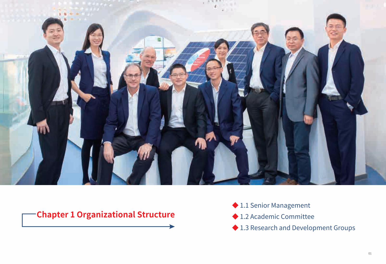
◆ 1.1 Senior Management◆ 1.2 Academic Committee◆ 1.3 Research and Development Groups
Chapter 1 Organizational Structure
01
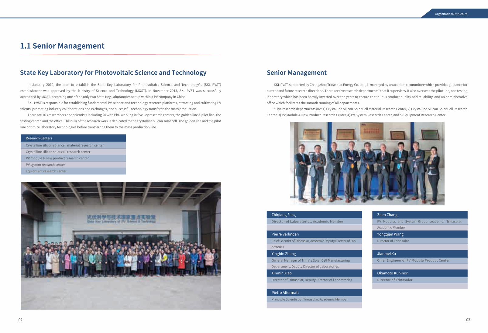
In January 2010, the plan to establish the State Key Laboratory for Photovoltaics Science and Technology’s (SKL PVST)
establishment was approved by the Ministry of Science and Technology (MOST). In November 2013, SKL PVST was successfully
accredited by MOST, becoming one of the only two State Key Laboratories set up within a PV company in China.
SKL PVST is responsible for establishing fundamental PV science and technology research platforms, attracting and cultivating PV
talents, promoting industry collaborations and exchanges, and successful technology transfer to the mass production.
There are 163 researchers and scientists including 20 with PhD working in five key research centers, the golden line & pilot line, the
testing center, and the office. The bulk of the research work is dedicated to the crystalline silicon solar cell. The golden line and the pilot
line optimize laboratory technologies before transferring them to the mass production line.
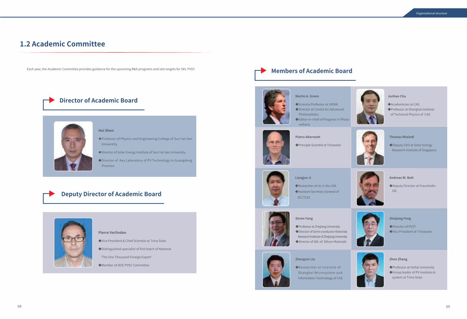
SKL PVST, supported by Changzhou Trinasolar Energy Co. Ltd., is managed by an academic committee which provides guidance for
current and future research directions. There are five research departments* that it supervises. It also oversees the pilot line, one testing
laboratory which has been heavily invested over the years to ensure continuous product quality and reliability, and an administrative
office which facilitates the smooth running of all departments.
*Five research departments are: 1) Crystalline Silicon Solar Cell Material Research Center, 2) Crystalline Silicon Solar Cell Research
Center, 3) PV Module & New Product Research Center, 4) PV System Research Center, and 5) Equipment Research Center.
Research Centers
Crystalline silicon solar cell material research center
Crystalline silicon solar cell research center
PV module & new product research center
PV system research center
Equipment research center
Pierre Verlinden
03 02
学术委员会Organizational structure
State Key Laboratory for Photovoltaic Science and Technology Senior Management
1.1 Senior Management
Chief Scientist of Trinasolar, Academic Deputy Director of Lab-
oratories
Pietro AltermattPrinciple Scientist of Trinasolar, Academic Member
Yingbin ZhangGeneral Manager of Trina’s Solar Cell Manufacturing
Department, Deputy Director of Laboratories
Zhiqiang FengDirector of Laboratories, Academic Member
Zhen Zhang PV Modules and System Group Leader of Trinasolar,
Academic Member
Yongqian WangDirector of Trinasolar
Jianmei XuChief Engineer of PV Module Product Center
Okamoto KuninoriDirector of Trinasolar
Xinmin XiaoDirector of Trinasolar, Deputy Director of Laboratories
Each year, the Academic Committee provides guidance for the upcoming R&D programs and sets targets for SKL PVST.
Hui Shen
◆Professor of Physics and Engineering College of Sun Yat-Sen Universtity
◆Director of Solar Energy Institute of Sun Yat-Sen University
◆Director of Key Laboratory of PV Technology in Guangdong Province
Pierre Verlinden
◆Vice President & Chief Scientist at Trina Solar
◆Distinguished specialist of first batch of National
'The One Thousand Foreign Expert'
◆Member of IEEE PVSC Committee
Deputy Director of Academic Board
Director of Academic Board
Members of Academic Board
1.2 Academic Committee
Thomas Rheindl
◆Deputy CEO at Solar Energy Research Institute of Singapore
Andreas W. Bett
◆Deputy Director at Fraunhofer ISE
Liangjun Ji
◆Researcher at UL in the USA
◆Assistant Secretary-General of
IEC/TC82
Pietro Altermatt
◆Principle Scientist at Trinasolar
Martin A. Green
◆Scientia Professor at UNSW ◆Director at Centre for Advanced Photovoltaics ◆Editor-in-chief of Progress in Photo- voltacis
Zhen Zhang
◆Professor at Hohai University◆Group leader of PV modules & system at Trina Solar
Zhengxin Liu
◆Researcher at Institute of Shanghai Microsystem and Information Technology of CAS
Zhiqiang Feng
◆Director of PVST◆Vice President at Trinasolar
05 04
Organizational structure
Junhao Chu
◆Academician at CAS◆Professor at Shanghai Institute of Technical Physics of CAS
Deren Yang
◆Professor at Zhejiang University ◆Director of Semi-conductor Materials Research Institute of Zhejiang University ◆Director of SKL of Silicon Materials
1.3 Research and Development Groups
Crystalline silicon solar cell re-
search center is responsible for the re-
search of crystalline silicon solar cell
structures ready for commercialisation
which involves theoretical simulation
and characterization of high-efficiency
solar cell structures. It is also respon-
sible for the development of key solar
cell processes such as light-trapping,
multi-layer passivation and metalliza-
tion, as well the research of reliability
and degradation mechanisms. Signifi-
cant technical breakthroughs have been
achieved on IBC, HIT and PERC solar
cells in recent years that broke several
Crystalline Silicon Solar Cell Research CenterPV system research center focuses
on developing and optimizing smart PV
modules & systems, and PV system
tests. In particular, the group focuses on
developing differentiated PV system
components that promote low LCOE.
The group routinely maintains the PV
system testing laboratory which asse-
sses system components’ engineering
and operation in both indoor and out-
door settings, and provides consult-
ation to Trinasolar's sales group on syst-
em design and component selection.
The latest achievements include
“internet-plus” applications, a 1500V PV
station, smart PV system for households
and participation in PV system standa-
rds.
PV System Research Center
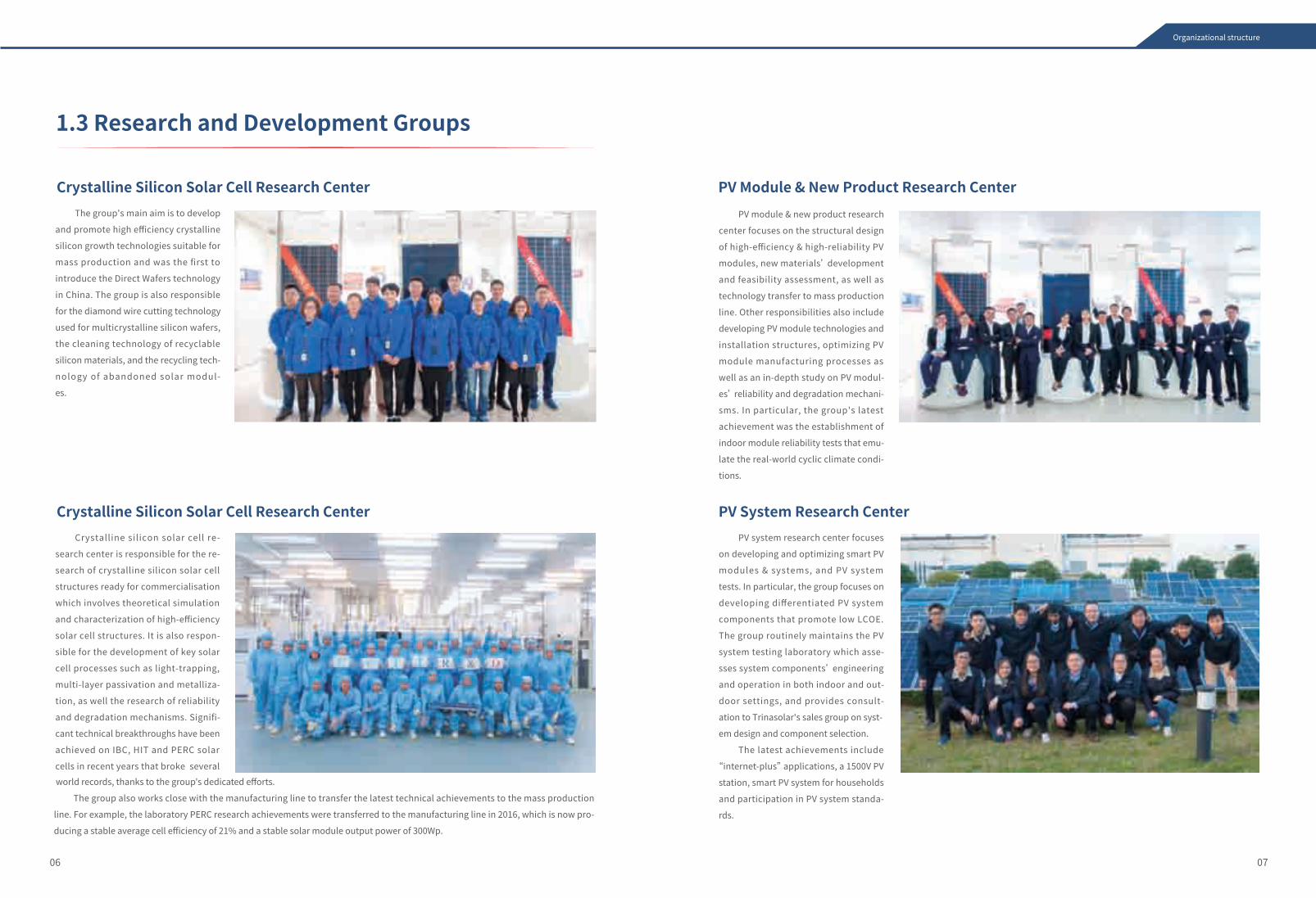
The group's main aim is to develop
and promote high efficiency crystalline
silicon growth technologies suitable for
mass production and was the first to
introduce the Direct Wafers technology
in China. The group is also responsible
for the diamond wire cutting technology
used for multicrystalline silicon wafers,
the cleaning technology of recyclable
silicon materials, and the recycling tech-
nology of abandoned solar modul-
es.
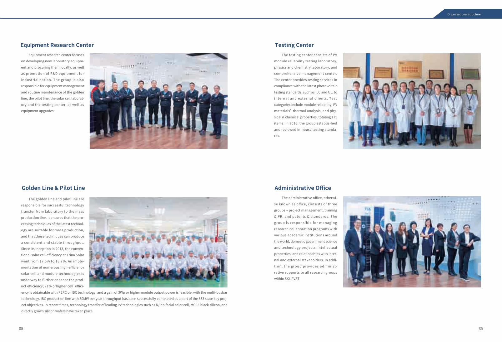
Crystalline Silicon Solar Cell Research CenterPV module & new product research
center focuses on the structural design
of high-efficiency & high-reliability PV
modules, new materials’ development
and feasibility assessment, as well as
technology transfer to mass production
line. Other responsibilities also include
developing PV module technologies and
installation structures, optimizing PV
module manufacturing processes as
well as an in-depth study on PV modul-
es’ reliability and degradation mechani-
sms. In particular, the group's latest
achievement was the establishment of
indoor module reliability tests that emu-
late the real-world cyclic climate condi-
tions.
PV Module & New Product Research Center
07 06
Organizational structure
world records, thanks to the group's dedicated efforts.
The group also works close with the manufacturing line to transfer the latest technical achievements to the mass production
line. For example, the laboratory PERC research achievements were transferred to the manufacturing line in 2016, which is now pro-
ducing a stable average cell efficiency of 21% and a stable solar module output power of 300Wp.
Golden Line & Pilot Line
Equipment research center focuses
on developing new laboratory equipm-
ent and procuring them locally, as well
as promotion of R&D equipment for
industrialisation. The group is also
responsible for equipment management
and routine maintenance of the golden
line, the pilot line, the solar cell laborat-
ory and the testing center, as well as
equipment upgrades.
The golden line and pilot line are
responsible for successful technology
transfer from laboratory to the mass
production line. It ensures that the pro-
cessing techniques of the latest technol-
ogy are suitable for mass production,
and that these techniques can produce
a consistent and stable throughput.
Since its inception in 2013, the conven-
tional solar cell efficiency at Trina Solar
went from 17.5% to 18.7%. An imple-
mentation of numerous high-efficiency
solar cell and module technologies is
underway to further enhance the prod-
uct efficiency; 21% orhigher cell effici-
ency is obtainable with PERC or IBC technology, and a gain of 3Wp or higher module output power is feasible with the multi-busbar
technology. IBC production line with 30MW per year throughput has been successfully completed as a part of the 863 state key proj-
ect objectives. In recent times, technology transfer of leading PV technologies such as N/P bifacial solar cell, MCCE black silicon, and
directly grown silicon wafers have taken place.
Equipment Research CenterThe testing center consists of PV
module reliability testing laboratory,
physics and chemistry laboratory, and
comprehensive management center.
The center provides testing services in
compliance with the latest photovoltaic
testing standards, such as IEC and UL, to
internal and external cl ients. Test
categories include module reliability, PV
materials’ thermal analysis, and phy-
sical & chemical properties, totaling 175
items. In 2016, the group establis-hed
and reviewed in-house testing standa-
rds.
The administrative office, otherwi-
se known as office, consists of three
groups ‒ project management, training
& PR, and patents & standards. The
group is responsible for managing
research collaboration programs with
various academic institutions around
the world, domestic government science
and technology projects, intellectual
properties, and relationships with inter-
nal and external stakeholders. In addi-
tion, the group provides administ-
rative supports to all research groups
within SKL PVST.
Testing Center
Administrative Office
09 08
Organizational structure
11
Chapter 2 Research Updates
◆ 2.1 Crystalline Silicon Solar Cell Material Research Center
◆ 2.2 Crystalline Silicon Solar Cell Research Center
◆ 2.3 PV Module & New Product Research Center
◆ 2.4 PV System Research Center
◆ 2.5 Equipment Research Center
2.1 Bulk lifetime of a silicon brick
Measurement of minority carrier lifetime involves optical
excitation and signal detection. μ-PCD (Microwave Photocon-
ductivity Decay) and QSSPC (Quasi Steady State Photoconduc-
tance) are common methods used as lifetime measurements.
With μ-PCD, the pulse of an infrared semiconductor laser
(904nm wavelength) generates free electron-hole pairs on an
illuminated sample area, and the decaying conductivity can be
monitored by the microwave reflectance detector. With QSSPC,
the sample is illuminated with an IR-Pass filtered Xenon flash
lamp while the photoconductance is measured simultaneously
by an eddy current conductance sensor [1]. The measurement
depth of QSSPC is approximately 3mm while that of μ-PCD is
approximately 30μm. Since the dimensions of silicon brick,
156mm×156mm×360mm, is much deeper than the carrier
injection depth and the effective carrier lifetime measurement is
not affected by the wafer surface condition, the minority carrier
lifetime estimated can be directly measure the silicon brick.
As shown in Figure 1, the carrier lifetime alongside the
crystal growth direction of silicon brick increases initially before
peaking at approximately 15cm deep into the brick, then
declines. The low carrier lifetime at the bottom of the brick
could be attributed to the presence of impurities diffused from
the crucible and deep-level recombination centers created as a
result. The low carrier lifetime at the top is caused by the
directional solidification of impurities during the crystal growth
process, accompanied by the presence of dislocations and
recombination centers.
12
There is a strong relationship between the efficiency of
solar cell and its minority carrier lifetime. The minority carrier
lifetime is mainly affected by impurities, dislocations, and grain
boundaries where recombination thrives. Imrpoving minority
carrier lifetime of silicon will improve the efficiency of solar cell.
In order to obtain a high minority carrier lifetime of silicon,
the silicon crystal growth process needs to be monitored to
control the impurity content and the dislocation density.
However, it is difficult to directly control the silicon crystal
growth process. In 2016, a multi-crystalline silicon (mc-Si) wafer
with a high minority carrier lifetime was successfully procured
by employing homogeneous nucleation technology. Charact-
erization of a high minority carrier lifetime of mc-Si was carried
out for an in-depth analysis of high performance silicon crystal.
The minority carrier lifetime is an important characterization parameter to determine the quality of silicon crystal. A silicon wafer with
a high minority carrier lifetime guarantees a high-efficiency solar cell and a maximum power output generating module. In 2016, Trina
solar developed an innovative T1 wafer with an optimized crystal growth process. The average minority carrier lifetime could reach up
to 500μs ~ 600μs, one of the highest in PV industry. This paper also presents different measuring techniques of minority carrier lifetime
for silicon. An effective characterization is a powerful tool for the development of advanced and innovative manufacturing technolo-
gies.
1. Background
Characterization of high minority carrier lifetime of multi-crystalline silicon
Qiuxiang He, Hua Zhang, Zhen Xiong
Analysis of a highly reliable PV tracking system /38Correlation of modules’ long-term reliability with indoor acc-elerated aging tests / 41Reliability of silicone structural adhesive in PV modules / 45 Reliability of polyolefin encapsulant in a PV module / 48Development of sahara module with high wearability / 51
2.4 PV System Research Center / 55 Research and development of PV system integration products in the distributed residential market / 55Evaluation of energy performance & reliability of PV systems with various types of PV modules in typical climates / 59LCOE modeling and analysis of the main influence factors / 63
2.5 Equipment Research Center / 66R&D of c-Si PV manufacturing equipment and its progress / 66PTP (pattern transfer printing) technology for a novel selecti-ve emitter finger alignment / 69
2.1 Crystalline Silicon Solar Cell Material Research Center2.1 Crystalline Silicon Solar Cell Mate-rial Research Center / 13Characterization of high minority carrier lifetime of multicrysta-lline silicon / 13Hetero-seed-assisted growth of high-performance multicrystal-line silicon in directional solidification / 19
2.2 Crystalline Silicon Solar Cell Resear-ch Center / 22R&D and industrialization of P-type PERC solar cells / 22 High-efficiency N-PERT solar cells and industrilization / 26R&D of IBC solar cell, module and its application / 26Perovskite solar cells / 34
2.3 PV Module & New Product Research Center / 38
13
Research updates
2. Characterization of high minority carrier lifetime silicon
Figure 1
The change of minority carrier lifetime alongside the crystal growth
direction of silicon brick
There is a strong relationship between the efficiency of
solar cell and its minority carrier lifetime. The minority carrier
lifetime is mainly affected by impurities, dislocations, and grain
boundaries where recombination thrives. Imrpoving minority
carrier lifetime of silicon will improve the efficiency of solar cell.
In order to obtain a high minority carrier lifetime of silicon,
the silicon crystal growth process needs to be monitored to
control the impurity content and the dislocation density.
However, it is difficult to directly control the silicon crystal
growth process. In 2016, a multi-crystalline silicon (mc-Si) wafer
with a high minority carrier lifetime was successfully procured
by employing homogeneous nucleation technology. Charact-
erization of a high minority carrier lifetime of mc-Si was carried
out for an in-depth analysis of high performance silicon crystal.
14
2.2 PL imaging of silicon brick
The brick PL imaging equipment developed by BT Imaging
Company is a fast, spatially resolved and sensitive measuring
tool that could be employed to measure the whole cross-section
of the silicon brick [2]. Photoluminescence of crystalline silicon
is caused by radiative recombination of photo-excited electron
‒hole pairs. The radiative component of the recombination of
excess charge carriers, △n, can be detected with a Si-CCD cam-
era. Recombination centers in crystal could reduce electron
‒hole pairs, showing up as dark spots on a PL image.
The formation of dislocation during the crystal growth
process, and carrier recombinations in the brick are clearly
shown on the brick PL image. Figure 2 illustrates different PL
images of (a) high carrier lifetime of a brick and (b) low carrier
lifetime of a brick. The dislocation density of the high-lifetime
brick is lower than that of the low-lifetime brick.
In addition, precise locations of the dislocation density and
the impurity density can be obtained with a special calculation
based on the PL imaging; the result is shown in Figure 3.
3.1 Bulk lifetime of a wafer with high minority carrier lifetime
For as-cut silicon wafers, the effective carrier lifetime is
largely limited by cut surface of the wafer where dangling bonds
can easily be introduced to. Usually, the defect density of the
surface is higher than that of the bulk [3]. It is essential to
minimize the surface recombination to get an effective carrier
lifetime. The relationship between the effective carrier lifetime
and the bulk carrier lifetime is as follows [4]:
3.2 The effect of phosphorus diffusion gettering
The phosphorus diffusion process is not only a useful pro-
cessing step to fabricate P-N junction for a P-type silicon sub-
strate but also an effective way to reduce metal impurities in sili-
con [5]. The carrier lifetime of a gettered silicon wafer could be
an effective indicator for its solar cell efficiency. Adjacent wafers
in the silicon brick with high carrier lifetime are divided into two
groups. Group1 is processed without gettering, and Group2 is
processed with gettering. Results of the carrier lifetime of the
two groups are shown in Figure 4. For a high carrier lifetime
wafer, the minority carrier diffusion length is increased by get-
tering, and subsequent improvement of carrier lifetime [6]. In
addition, the concentration of interstitial Fe declines from
3×10¹⁰ ~ 1×1011 cm-3 to a negligible value for a P-diffused silicon
brick.
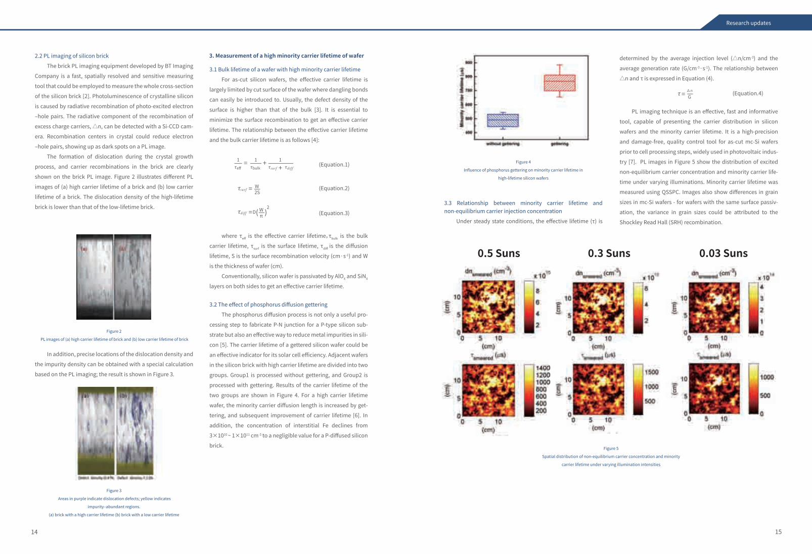
3.3 Relationship between minority carrier lifetime and non-equilibrium carrier injection concentration
Under steady state conditions, the effective lifetime (τ) is
PL imaging technique is an effective, fast and informative
tool, capable of presenting the carrier distribution in silicon
wafers and the minority carrier lifetime. It is a high-precision
and damage-free, quality control tool for as-cut mc-Si wafers
prior to cell processing steps, widely used in photovoltaic indus-
try [7]. PL images in Figure 5 show the distribution of excited
non-equilibrium carrier concentration and minority carrier life-
time under varying illuminations. Minority carrier lifetime was
measured using QSSPC. Images also show differences in grain
sizes in mc-Si wafers - for wafers with the same surface passiv-
ation, the variance in grain sizes could be attributed to the
Shockley Read Hall (SRH) recombination.
determined by the average injection level (△n/cm-3) and the
average generation rate (G/cm-3·s-1). The relationship between
△n and τ is expressed in Equation (4).
where τeff is the effective carrier lifetime,τbulk is the bulk
carrier lifetime, τsurf is the surface lifetime, τdiff is the diffusion
lifetime, S is the surface recombination velocity (cm·s-1) and W
is the thickness of wafer (cm).
Conventionally, silicon wafer is passivated by AlOX and SiNX
layers on both sides to get an effective carrier lifetime.
3. Measurement of a high minority carrier lifetime of wafer
Figure 2
PL images of (a) high carrier lifetime of brick and (b) low carrier lifetime of brick
Figure 3
Areas in purple indicate dislocation defects; yellow indicates
impurity‒abundant regions.
(a) brick with a high carrier lifetime (b) brick with a low carrier lifetime
Research updates
15
Figure 4
Influence of phosphorus gettering on minority carrier lifetime in
high-lifetime silicon wafers
Figure 5
Spatial distribution of non-equilibrium carrier concentration and minority
carrier lifetime under varying illumination intensities
∆n (Equation.4)
0.5 Suns 0.3 Suns 0.03 Suns
1eff
= 1bulk
1sur f
sur f
d i f f+
+ (Equation.1)
= W
G
2S
=
di f f = WDπ
(Equation.2)
(Equation.3)( )2
15
1716
References
[1] Sinton R A, Cuevas A, Contactless Determination of Current‒voltage Characteristics and Minority Carrier Lifetimes in Semiconductors from Quasi‐steady-state Photoconductance Data, Applied Physics Letters, 1996, 69(17):2510-2512.
[2] Mitchell B, Trupke T, Weber J W, et al., Bulk Minority Carrier Lifetimes and Doping of Silicon Bricks from Photoluminescence Intensity Ratios, Journal of Applied Physics, 2011, 109(8):083111-083111-12.
[3] Zeng S R. Basic Physical of Semiconductor [M]. Peking University Press, 2007.
[4] Grivickas V, Noreika D, Tellefsen J A. Surface and Auger recombination in silicon wafers of high carrier density [J]. Lithuanian Physics Journal, 1989, 29: 48‒53.
[5] Cuevas A, Macdonald D, Kerr M, et al., Evidence of Impurity Gettering by Industrial Phosphorus diffusion, 28th Photovoltaic Specialists Conference, 2000:244-247.
[6] Sio H C, Macdonald D. Direct Comparison of the Electrical Properties of Multicrystalline Silicon Materials for Solar Cells: Conventional p-type, n-type and High Performance p-type [J]. Solar Energy Materials & Solar Cells, 2016, 144:339-346.
[7] Lim S Y, Forster M, Zhang X, et al. Applications of Photoluminescence Imaging to Dopant and Carrier Concentration Measurements of Silicon Wafers[J]. IEEE Journal of Photovoltaics, 2013, 3(2):649-655.
[8] Haunschild J, Glatthaar M, Demant M, et al. Quality Control of As-cut Multicrystalline Silicon Wafers Using Photoluminescence Imaging for Solar Cell production [J]. Solar Energy Materials & Solar Cells, 2007, 94(12):2007-2012.
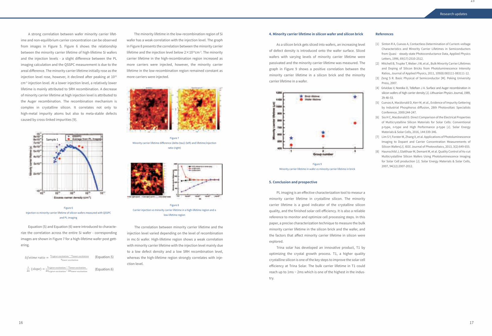
As a silicon brick gets sliced into wafers, an increasing level
of defect density is introduced onto the wafer surface. Sliced
wafers with varying levels of minority carrier lifetime were
passivated and the minority carrier lifetime was measured. The
graph in Figure 9 shows a positive correlation between the
minority carrier lifetime in a silicon brick and the minority
carrier lifetime in a wafer.
4. Minority carrier lifetime in silicon wafer and silicon brick
PL imaging is an effective characterization tool to measur a
minority carrier lifetime in crystalline silicon. The minority
carrier lifetime is a good indicator of the crystalline silicon
quality, and the finished solar cell efficiency. It is also a reliable
reference to monitor and optimize cell processing steps. In this
paper, a precise characterization technique to measure the bulk
minority carrier lifetime in the silicon brick and the wafer, and
the factors that affect minority carrier lifetime in silicon were
explored.
Trina solar has developed an innovative product, T1 by
optimizing the crystal growth process. T1, a higher quality
crystalline silicon is one of the key steps to improve the solar cell
efficiency at Trina Solar. The bulk carrier lifetime in T1 could
reach up to 1ms ~ 2ms which is one of the highest in the indus-
try.
5. Conclusion and prospective
A strong correlation between wafer minority carrier lifet-
ime and non-equilibrium carrier concentration can be observed
from images in Figure 5. Figure 6 shows the relationship
between the minority carrier lifetime of high-lifetime Si wafers
and the injection levels - a slight difference between the PL
imaging calculation and the QSSPC measurement is due to the
areal difference. The minority carrier lifetime initially rose as the
injection level rose, however, it declined after peaking at 1015
cm-3 injection level. At a lower injection level, a relatively lower
lifetime is mainly attributed to SRH recombination. A decrease
of minority carrier lifetime at high injection level is attributed to
the Auger recombination. The recombination mechanism is
complex in crystalline silicon. It correlates not only to
high-metal impurity atoms but also to meta-stable defects
caused by cross-linked impurities [9].
The correlation between minority carrier lifetime and the
injection level varied depending on the level of recombination
in mc-Si wafer. High-lifetime region shows a weak correlation
with minority carrier lifetime with the injection level mainly due
to a low defect density and a low SRH recombination level,
whereas the high-lifetime region strongly correlates with inje-
ction level.
Equation (5) and Equation (6) were introduced to characte-
rize the correlation across the entire Si wafer - corresponding
images are shown in Figure 7 for a high-lifetime wafer post gett-
ering.
The minority lifetime in the low-recombination region of Si
wafer has a weak correlation with the injection level. The graph
in Figure 8 presents the correlation between the minority carrier
lifetime and the injection level below 2×1014cm-3. The minority
carrier lifetime in the high-recombination region increased as
more carriers were injected, however, the minority carrier
lifetime in the low-recombination region remained constant as
more carriers were injected.
晶体硅光伏技术研究成果Research updates
Figure 7
Minority carrier lifetime difference (delta (tau)) (left) and lifetime/injection
ratio (right)
Figure 9
Minority carrier lifetime in wafer vs minority carrier lifetime in brick
Figure 8
Carrier injection vs minority carrier lifetime in a high-lifetime region and a
low-lifetime region
Figure 6
Injection vs minority carrier lifetime of silicon wafers measured with QSSPC
and PL imaging
1Sample
(Equation.6)
(Equation.5)
Since its conception, the crystalline silicon grown by di-rectional solidification has undergone three main stages of de-velopment: 1) the conventional casting multi-crystalline sili-con (mc-Si) with no given seeds, 2) the quasi-single crystalline silicon (QSC-Si) with mono-crystalline silicon bricks or blocks as seeds [1-5] and 3) the high-performance multi-crystalline silicon (HP mc-Si) with polycrystalline or multi-crystalline sil-icon (silicon powder, particles or fragments) as seeds [6-10]. The cell conversion efficiency improved using both the QSC casting methodand the HP casting method ‒ the QSC casting method decreased the grain boundary fractions while the HP casting method reduced dislocation densities in the crystal. However, the QSC casting method, limited by the single crystal area ratio and the production cost, was not ideal for mass pro-duction. Thus, the HP casting method, due to its high cost-ef-fectiveness, has now been widely adopted in the industry.
It is well recognized that cultivating the columnar grains in parallel growth directions is an effective way to suppress the generation and propagation of dislocations, which would be a great breakthrough for improving the crystal quality of mc-Si [6, 7, 9, 11]. HP mc-Si was developed based on a low dislocation density crystal grown by the seed-assisted method. The seed-ing step, which determines the initial grain shape distribution, is quite essential for the growth of columnar grains. Both homo-seeding and hetero-seeding methods have been developed to assist the growth of columnar grains which are considered ca-pable of absorbing stress [6, 7, 9]. Due to its simple operation, a short processing cycle and a high ingot casting yield, the het-ero-seeding is expected to be a promising seeding method.
Usually, the homo-seeding displays good seeding effect,
however, the melting process must be precisely controlled to
make sure that enough silicon seeds are preserved and the
melting/growth fronts are as flat as possible. In contrast, since
no silicon seeds need to be preserved, the hetero-seeding is
more suitable to rapid melting processes.
The innate distinction between the hetero-seeding and the
homo-seeding is whether the nucleation process is involved
during the directional solidification. The nucleation refers to the
initial stage of crystallization: under a certain degree of under-
cooling with temperature and concentration fluctuations, some
atoms of the melt gather and reach to a critical size and become
solid particles. The surrounding atoms then could pile up to
further reduce the free energy of these atoms that formed the
nuclei. For the homo-seeding process, the silicon crystal (the
seeds) always exists during melting process, and the silicon
crystal epitaxially grow into a complete ingot in the subsequent
directional solidification steps without going through the nucle-
ation process. For the hetero-seeding process, since all silicon
feedstock is melted before crystallization, the nucleation
process is inevitable. A controlled nucleation process is quite
important for the subsequent crystal growth of columnar grains.
The architecture of the advanced seeding layer, the control
of growth fronts and the degree of undercooling enable the
efficiency of the solar cell obtained from the hetero-seeding
method to be as high as that obtained from the homo-seeding
method. Therefore, the hetero-seed-assisted growth of
high-performance multi-crystalline is gaining an increasing
attention. However, compared to the homo-seeding method,
two intrinsic characteristics of the hetero-seeding method, the
instability of seeding effect and the sticking risk, are considered
the two biggest challenges of the hetero-seeding method. Table
1 shows the mainstream homo- and hetero-seeding materials
used for growth of HP mc-Si in directional solidification. The
seeding mechanisms and the seeding effects with different seed
materials will be discussed in detail in the following sections.Over the past years, due to its cost-effectiveness, the high-performance multi-crystalline silicon (HP mc-Si) ingots grown in directional
solidification has been the main material for photovoltaic (PV) devices. The seeding process is considered to be the key step in the
growth of HP mc-Si which determines both the initial grain shape distribution and the dislocation density level of silicon crystal. The
heterogeneous seed-assisted crystal growth (hetero-seeding) technology is becoming the promising casting method for PV silicon
ingots for its simple operation, short process cycle, and high ingot casting yield. In this paper, we review the research progress of
hetero-seeding technology for HP mc-Si growth. Fused silica particles have been widely used as a hetero-seed as its resultant solar cell
conversion efficiency can be as high as that obtainable from the homogeneous seeding (homo-seeding) growth. However, some
defects in fused silica, such as the oxygen contamination, limit the quality of solar cell. We propose SiC and Al2O3 to be used as the
seeding material instead of fused silica.
1. Background of seed assisted HP mc-Si
According to recent studies [12-14], uniform columnar
grains could be obtained by optimizing the types and the
particle sizes of the seed, the thermal field structure and the
crystal growth process using hetero-seeding directional solidifi-
cation system. Hetero-seeding structures could be divided into
two groups: the bared-particles seeding (bp-seeding) and the
covered-particles seeding (cp-seeding).
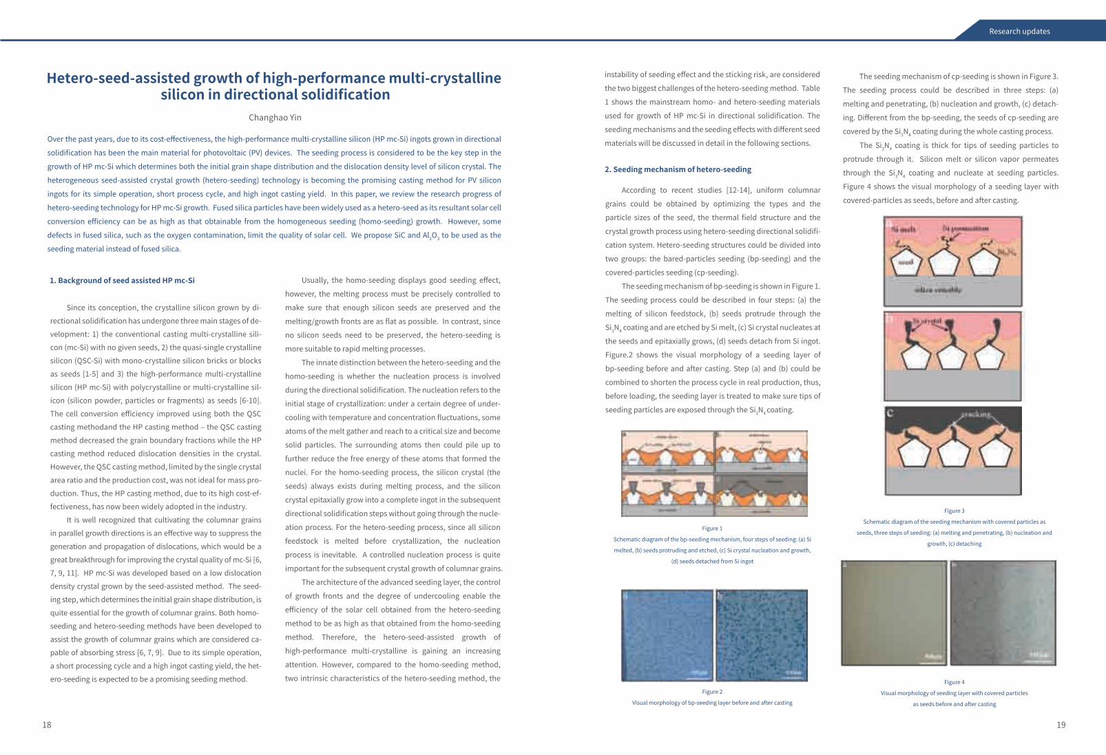
The seeding mechanism of bp-seeding is shown in Figure 1.
The seeding process could be described in four steps: (a) the
melting of silicon feedstock, (b) seeds protrude through the
Si3N4 coating and are etched by Si melt, (c) Si crystal nucleates at
the seeds and epitaxially grows, (d) seeds detach from Si ingot.
Figure.2 shows the visual morphology of a seeding layer of
bp-seeding before and after casting. Step (a) and (b) could be
combined to shorten the process cycle in real production, thus,
before loading, the seeding layer is treated to make sure tips of
seeding particles are exposed through the Si3N4 coating.
2. Seeding mechanism of hetero-seeding
Hetero-seed-assisted growth of high-performance multi-crystalline silicon in directional solidification
Changhao Yin
1918
Research updates
Figure 1
Schematic diagram of the bp-seeding mechanism, four steps of seeding: (a) Si
melted, (b) seeds protruding and etched, (c) Si crystal nucleation and growth,
(d) seeds detached from Si ingot
Figure 3
Schematic diagram of the seeding mechanism with covered particles as
seeds, three steps of seeding: (a) melting and penetrating, (b) nucleation and
growth, (c) detaching
Figure 4
Visual morphology of seeding layer with covered particles
as seeds before and after casting
Figure 2
Visual morphology of bp-seeding layer before and after casting
The seeding mechanism of cp-seeding is shown in Figure 3.
The seeding process could be described in three steps: (a)
melting and penetrating, (b) nucleation and growth, (c) detach-
ing. Different from the bp-seeding, the seeds of cp-seeding are
covered by the Si3N4 coating during the whole casting process.
The Si3N4 coating is thick for tips of seeding particles to
protrude through it. Silicon melt or silicon vapor permeates
through the Si3N4 coating and nucleate at seeding particles.
Figure 4 shows the visual morphology of a seeding layer with
covered-particles as seeds, before and after casting.
Both bp-seeding and cp-seeding could be used to form
uniform columnar grains. The advantage of bp-seeding is that
the silicon melt could easily contact with seeds, therefore, the
heating and melting cycles could be shortened, while the
cp-seeding needs more holding time after the melting to ensure
that enough silicon penetrates through the Si3N4 coating and nucleates. However, due to a direct contact between the melt
and seeds leading to a direct contact between the silicon ingot
and seeds, the bp-seeding is usually associated with a high risk
of sticking.
In order to obtain a better seeding effect, types of seeding
materials have been investigated. It is necessary to consider
following factors for seeding materials: the wettability between
seeds and the silicon melt, the melting point of seeds and the
purity of seeds. Studies [15, 16] have shown that a variety of
refractories show good wettability to silicon melt, however, only
few of them could be a good candidate for a seeding material,
subject to its purity and attachability to the silica crucible. Table
1 shows common seeding materials used for the HP mc-Si
growth in directional solidification.
At present, the fused silica is widely used as the seeding
material to assist the growth of HP mc-Si in industry, mainly
shows better wettability to the silicon melt(θ<90°)than fused
silica(θ≈90°)[15] and hardly causes the oxygen contamination,
SiC is considered to be a promising seeding material. However,
controlling the purity may be the biggest challenge for SiC as a
seeding material.
Al2O3 is another candidate for a seeding material. Since
Al2O3 can be processed into perfect spherical particles, Al2O3
seeds could be arranged uniformly onto the silica crucible to
form a more textured seeding layer, which is expected to benefit
the silicon grain size distribution. Also, since the element Al is an
acceptor impurity in silicon crystal, Al2O3 seeds may help reduce
the resistivity at the bottom of the ingot.
3. Seeding materials for hetero-seeding
For silicon crystal growth, a successful seeding is a prereq-
uisite for growing columnar grains. The subsequent directional
solidification is also important to the crystal quality [17, 18].
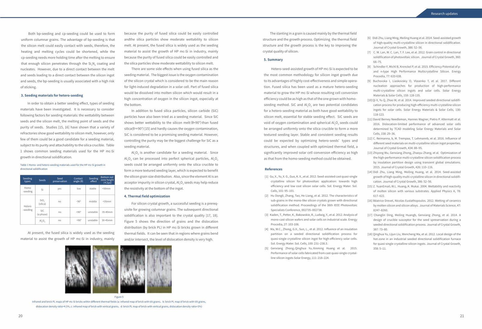
Figure 5 shows the direction of grains and the dislocation
distribution (by brick PL) in HP mc-Si bricks grown in different
thermal fields. It can be seen that in regions where grains bend
and/or intersect, the level of dislocation density is very high.
The slanting in a grain is caused mainly by the thermal field
structure and the growth process. Optimizing the thermal field
structure and the growth process is the key to improving the
crystal quality of silicon.
4. Thermal field optimization
Hetero-seed-assisted growth of HP mc-Si is expected to be
the most common methodology for silicon ingot growth due
to its advantages of highly cost-effectiveness and simple opera-
tion. Fused silica has been used as a mature hetero-seeding
material to grow the HP mc-Si whose resulting cell conversion
efficiency could be as high as that of the one grown with homo-
seeding method. SiC and Al2O3 are two potential condidates
for a hetero-seeding material as both have good wettability to
silicon melt, essential for stable seeding effect. SiC seeds are
void of oxygen contamination and spherical Al2O3 seeds could
be arranged uniformly onto the silica crucible to form a more
textured seeding layer. Stable and consistent seeding results
could be expected by optimizing hetero-seeds’ types and
structures, and when coupled with optimized thermal field, a
significantly improved solar cell conversion efficiency as high
as that from the homo-seeding method could be obtained.
5. Summary
2120
References
[1] Gu, X., Yu, X. G., Guo, K. X., et al. 2012. Seed-assisted cast quasi-single crystalline silicon for photovoltaic application: towards high efficiency and low cost silicon solar cells. Sol. Energy Mater. Sol. Cells, 101: 95‒101.
[2] Hu Dongli, Zhang, Tao, He Liang, et al. 2012. The characteristics of sub-grains in the mono-like silicon crystals grown with directional solidification method. Proceedings of the 38th IEEE Photovoltaic Specialists Conference, 002735‒002738.
[3] Kaden, T., Petter, K., Bakowskie, R., Ludwig, Y., et al. 2012. Analysis of mono-cast silicon wafers and solar cells on industrial scale. Energy Procedia, 27: 103-108.
[4] Ma, W.C., Zhong, G.X., Sun, L., et al. 2012. Influence of an insulation partition on a seeded directional solidification process for quasi-single crystalline silicon ingot for high-efficiency solar cells. Sol. Energy Mater. Sol. Cells, 100: 231‒238.3.
[5] Genxiang Zhong,Qinghua Yu,Xinming Huang et al. 2015. Performance of solar cells fabricated from cast quasi-single crystal-line silicon ingots Solar Energy, 111: 218‒224.
[6] Didi Zhu, Liang Ming, Meiling Huang et al. 2014. Seed-assisted growth
of high-quality multi-crystalline silicon in directional solidification. Journal of Crystal Growth, 386: 52‒56.
[7] C. W. Lan, W. C. Lan, T. F. Lee, et al. 2012. Grain control in directional solidification of photovoltaic silicon. Journal of Crystal Growth, 360: 68‒75.
[8] Schindler F, Michl B, Krenckel P, et al. 2015. Efficiency Potential of p- and n-type High Performance Multicrystalline Silicon. Energy Procedia, 77: 633-638.
[9] Buchovska I, Liaskovskiy O, Vlasenko T, et al. 2017. Different nucleation approaches for production of high-performance multi-crystalline silicon ingots and solar cells. Solar Energy Materials & Solar Cells, 159: 128-135.
[10] Qi X, Yu Q, Zhao W, et al. 2014. Improved seeded directional solidifi-cation process for producing high-efficiency multi-crystalline silicon ingots for solar cells. Solar Energy Materials & Solar Cells, 130: 118-123.
[11] David Berney Needleman, Hannes Wagner, Pietro P. Altermatt et al. 2016. Dislocation-limited performance of advanced solar cells determined by TCAD modeling Solar Energy Materials and Solar Cells, 158: 29‒36.
[12] C. Reimanna, b, M. Trempaa, T. Lehmannb, et al. 2016. Influence of different seed materials on multi-crystalline silicon ingot properties. Journal of Crystal Growth, 434: 88‒95.
[13] Zhiyong Wu, Genxiang Zhong, Zhaoyu Zhang, et al. Optimization of the high-performance multi-crystalline silicon solidification process by insulation partition design using transient global simulations. 2015. Journal of Crystal Growth, 426: 110‒116.
[14] Didi Zhu, Liang Ming, Meiling Huang, et al. 2014. Seed-assisted growth of high-quality multi-crystalline silicon in directional solidifi-cation. Journal of Crystal Growth, 386: 52‒56.
[15] Z. YuanEmail,W.L. Huang,K. Mukai. 2004. Wettability and reactivity of molten silicon with various substrates. Applied Physics A, 78: 617‒622.
[16] Béatrice Drevet, Nicolas Eustathopoulos. 2012. Wetting of ceramics by molten silicon and silicon alloys. Journal of Materials Science, 47: 8247‒8260.
[17] Changlin Ding, Meiling Huangb, Genxiang Zhong, et al. 2014. A design of crucible susceptor for the seed spreservation during a seeded directional solidification process. Journal of Crystal Growth, 387: 73‒80.
[18] Qinghua Yu, Lijun Liu, Wencheng Ma, et al. 2012. Local design of the hot-zone in an industrial seeded directional solidification furnace for quasi-single crystalline silicon ingots. Journal of Crystal Growth, 358: 5‒11.
Research updates
Figure 5
Infrared and brick PL maps of HP mc-Si bricks within different thermal fields (a: infrared map of brick with tilt grains,b: brick PL map of brick with tilt grains,
dislocation density ratio>4.5%, c: infrared map of brick with vertical grains,d: brick PL map of brick with vertical grains, dislocation density ratio<3%)
Seedingtypes Seeds Seed
preservationSeeding
effectBottom red zone height
(≤2μs)Contactangle (θ)
yes low stable >50mm
no ~90° middle <35mm
no <90° unstable 35-40mm
no <90° unstable 30-45mm
Homo-seeding
Hetero-seeding
Si
SiO2
(silica)
SiC(α phase)
Al2O3
Table 1 Homo- and hetero-seeding materials used for the HP mc-Si growth in directional solidification
There are some side effects when using fused silica as the
seeding material. The biggest issue is the oxygen contamination
of the silicon crystal which is considered to be the main reason
for light-induced degradation in a solar cell. Part of fused silica
would be dissolved into molten silicon which would result in a
high concentration of oxygen in the silicon ingot, especially at
the bottom.
In addition to fused silica particles, silicon carbide (SiC)
particles have also been tried as a seeding material. Since SiC
because the purity of fused silica could be easily controlled
andthe silica particles show moderate wettability to silicon
melt. At present, the fused silica is widely used as the seeding
material to assist the growth of HP mc-Si in industry, mainly
because the purity of fused silica could be easily controlled and
the silica particles show moderate wettability to silicon melt.
The P-type Si PERC solar cell has received special attention
due to its cost-effectiveness. Compared with conventional BSF
solar cells, the rear surface recombination velocity is signifi-
cantly lower due to the introduction of passivated dielectric
layers. The resulting Voc and Isc have been promoted heavily,
along with the efficiency increase of 1% and 0.8% on a mono-
and a multi- Si substrates respectively. Another advantage is the
compatibility of its manufacturing equipment with the conven-
tional mass production equipment.
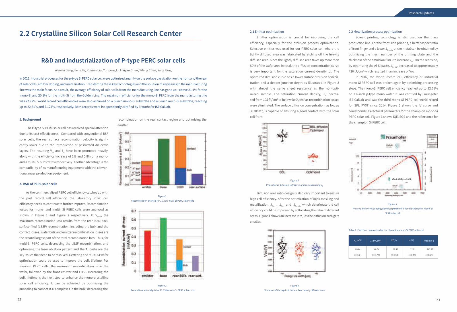
1. Background
As the commercialised PERC cell efficiency catches up with
the past record cell efficiency, the laboratory PERC cell
efficiency needs to continue to further improve. Recombination
losses for mono- and multi- Si PERC cells were analyzed as
shown in Figure 1 and Figure 2 respectively. At Vmpp, the
maximum recombination loss results from the rear local back
surface filed (LBSF) recombination, including the bulk and the
contact losses. Wafer bulk and emitter recombination losses are
the second largest part of the total recombination loss. Thus, for
multi-Si PERC cells, decreasing the LBSF recombination, and
optimizing the laser ablation pattern and the Al paste are the
key issues that need to be resolved. Gettering and multi-Si wafer
optimization could be used to improve the bulk lifetime. For
mono-Si PERC cells, the maximum recombination is in the
wafer, followed by the front emitter and LBSF. Increasing the
bulk lifetime is the next step to enhance the mono-crystalline
solar cell efficiency. It can be achieved by optimizing the
annealing to combat B-O complexes in the bulk, decreasing the
recombination on the rear contact region and optimizing the
emitter.
2. R&D of PERC solar cells
2322
In 2016, industrial processes for the p-type Si PERC solar cell were optimized, mainly on the surface passivation on the front and the rear
of solar cells, emitter doping, and metallization. Transferring these key technologies and the solution of key issues to the manufacturing
line was the main focus. As a result, the average efficiency of solar cells from the manufacturing line has gone up - above 21.1% for the
mono-Si and 20.1% for the multi-Si from the Golden Line. The maximum efficiency for the mono-Si PERC from the manufacturing line
was 22.22%. World record cell efficiencies were also achieved on a 6-inch mono-Si substrate and a 6-inch multi-Si substrate, reaching
up to 22.61% and 21.25%, respectively. Both records were independently certified by Fraunhofer ISE CalLab.
R&D and industrialization of P-type PERC solar cellsWeiwei Deng, Feng Ye, Ruimin Liu, Yunpeng Li, Haiyan Chen, Yifeng Chen, Yang Yang
Research updates
Figure 1
Recombination analysis for 21.25% multi-Si PERC solar cells
Figure 2
Recombination analysis for 22.13% mono-Si PERC solar cells
Figure 3
Phosphorus Diffusion ECV curve and corresponding J0
Figure 5
IV curve and corresponding electrical parameters for the champion mono-Si
PERC solar cell
Figure 4
Variation of Voc against the width of heavily diffused area
Table 1. Electrical parameters for the champion mono-Si PERC solar cell
2.2 Crystalline Silicon Solar Cell Research Center 2.1 Emitter optimization
Emitter optimization is crucial for improving the cell
efficiency, especially for the diffusion process optimization.
Selective emitter was used for our PERC solar cell where the
lightly diffused area was fabricated by etching off the heavily
diffused area. Since the lightly diffused area takes up more than
80% of the wafer area in total, the diffusion concentration curve
is very important for the saturation current density, J0. The
optimized diffusion curve has a lower surface diffusion concen-
tration and a deeper junction depth as illustrated in Figure 3
with almost the same sheet resistance as the non-opti-
mized sample. The saturation current density, J0, decrea-
sed from 105 fA/cm2 to below 60 fA/cm2 as recombination losses
were eliminated. The surface diffusion concentration, as low as
3E20cm-3, is capable of ensuring a good contact with the solar
cell front.
2.2 Metallization process optimization
Screen printing technology is still used on the mass
production line. For the front-side printing, a better aspect ratio
of front finger and a lower J0,metal under metal can be obtained by
optimizing the mesh number of the printing plate and the
thickness of the emulsion film - to increase Voc. On the rear side,
by optimizing the Al-Si paste, J0,LBSF decreased to approximately
420 fA/cm2 which resulted in an increase of Voc.
In 2016, the world record cell efficiency of industrial
mono-Si PERC cell was broken again by optimizing processing
steps. The mono-Si PERC cell efficiency reached up to 22.61%
on a 6-inch p-type mono wafer. It was certified by Fraungofer
ISE CalLab and was the third mono-Si PERC cell world record
for SKL PVST since 2014. Figure 5 shows the IV curve and
corresponding electrical parameters for the champion mono-Si
PERC solar cell. Figure 6 shows IQE, EQE and the reflectance for
the champion Si PERC cell.
Diffusion area ratio design is also very important to ensure
high cell efficiency. After the optimization of injek masking and
metallization, J0,n++, J0,n+ and J0,metal which deteriorate the cell
efficiency could be improved by collocating the ratio of different
areas. Figure 4 shows an increase in Voc as the diffusion area gets
smaller.
22.61%(±0.45%)
Voc(mV) Jsc(mA/cm2)
684.4
(±2.3)
40.54
(±0.77)
81.49
(±0.53)
22.61
(±0.45)
243.23
(±0.24)
FF(%) η(%) Area(cm2)
Currently, independently developed p-type mono-Si and
multi-Si solar cells have been steadily mass-manufactured. Our
future research direction focuses on the cost-effectiveness.
Research has been carried out in the Golden Line on
commercializing P-type PERC solar cells including the manage-
ment of the cleanliness of workshops, the equipment updates
that have gradually resolved the stability issue in the mass
production line, and the optimization of silicon wafers and
processing steps. Through optimization, the mono-Si and the
multi-Si cell efficiencies have increased from 20.4% and 18.8%
to 21.2% and 20.16%, respectively. Corresponding modules’
efficiencies have reached 300Wp and 285Wp, respectively.
3. Industrialization of PERC solar cell
A P-type bifacial PERC cell has characteristics of a conven-
tional high-efficiency single PN-junction PERC solar cell and as
the name suggests, can generate electricity on both front and
rear sides. Post processing optimization, the front cell efficiency
was approximately 21.2%, and the rear cell efficiency was
approximately 10%. The reliability tests are currently in
progress. The IV curve parameters of a pilot batch cell are shown
in Table 4.
4. R&D of industrial bifacial PERC solar cell
The main drive for the current R&D in PV is to improve the
efficiency while continuing on the effort to reduce the manufac-
turing cost. PERC solar cell has a large potential in this regard its
manufacturing cost is lower compared with other advanced
solar cell options. We hope to reach the goal of high-efficiency,
low-cost solar cell production through PERC R&D programs.
5. Summary
2524
Research updates
Figure 6
IQE, EQE and Reflectance of the champion mono-Si PERC solar cell
Figure 7
PERC cell contaminations
Figure 8
Saturation current density, J0, for pre- and post- diffusion optimization
Figure 9
Efficiency gain after optimization of rear laser pattern and pastes
Figure 10
Cell efficiency trend of mass production
Table 2. IV curve parameters pre- and post- diffusion optimization
Table 3. IV curve parameters of a mass produced mono- and multi-Si PERC cell and corresponding 60-cell modules
Table 4. IV curve parameters of a pilot p-type bifacial PERC solar cell
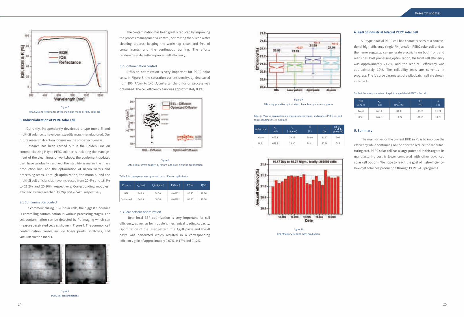
3.1 Contamination control
In commercializing PERC solar cells, the biggest hindrance
is controlling contamination in various processing stages. The
cell contamination can be detected by PL imaging which can
measure passivated cells as shown in Figure 7. The common cell
contamination causes include finger prints, scratches, and
vacuum suction marks.
3.3 Rear pattern optimization
Rear local BSF optimization is very important for cell
efficiency, as well as for module’s mechanical loading capacity.
Optimization of the laser pattern, the Ag/Al paste and the Al
paste was performed which resulted in a corresponding
efficiency gain of approximately 0.07%, 0.17% and 0.12%.
3.2 Contamination control
Diffusion optimization is very important for PERC solar
cells. In Figure 8, the saturation current density, J0, decreased
from 190 fA/cm2 to 140 fA/cm2 after the diffusion process was
optimized. The cell efficiency gain was approximately 0.1%.
The contamination has been greatly reduced by improving
the process management & control, optimizing the silicon wafer
cleaning process, keeping the workshop clean and free of
contaminants, and the continuous training. The efforts
rendered significantly improved cell efficiency.
Process Voc(mV) Jsc(mA/cm2) FF(%) η(%)Rs(Ohm)
BSL
Optimized
642.9
646.5
38.20
38.28
0.00171
0.00182
80.45
80.23
19.76
19.86
Wafer typeVoc
(mV)Jsc
(mA/cm2)FF
(%)η
(%)
60-cell module
power(W)
Mono
Multi
672.1
658.3
39.36
38.90
79.94
78.81
21.17
20.16
300
285
Test Surface
Voc
(mV)Jsc
(mA/cm2)FF
(%)η
(%)
Front
Rear
668.4
652.3
39.30
19.27
80.81
81.55
21.21
10.25
2726
The N-type solar cell has caught the attention of the indus-
try and institutions due to its high bulk lifetime and free-of-LID
characteristic. During the past decade, the development of
N-PERT solar cell has had a remarkable advancement. IMEC
reported 22.7% efficiency with a rear-emitter cell structure. In
2002, Zhao at UNSW reported that 21.9% efficiency was attained
with a front-emitter cell structure, two-side diffusion and passiv-
ation [1]. 22.7% efficiency with a rear-emitter cell structure
was reported subsequently [2]. In 2009, Fraunhofer laboratory
reported 23.4% efficiency on a 4 cm2 PERL cell [3]. Then in
2010, Fraunhofer laboratory reported 23.9% efficiency with a
front-emitter cell structure, Al2O3 passivation and Al/Ti/Pd/Ag
metallization [4]. This 23.9% efficiency is the highest recorded
efficiency for the PERL cell. The R&D progress of N-type bifacial
solar cells is announced frequently. At EUPVSEC in 2015, IMEC
published the paper on the bifacial solar cell with a Ni/Cu
plated rear emitter [5]. 22.5% efficiency was attained on the
6-inch wafer with resistivity of 5 Ω-cm-1. In 2016, the efficiency
improved to 22.6%.
N-type bifacial solar cells have a promising future for
commercialization. The significant advantage of the N-type
bifacial solar cell is 10~30% power gain, depending on applic-
ation circumstances, when compared with a conventional mono
-facial module. Present manufacturers of N-type bifacial solar
cells include Yingli, HT-SAAE, Inventec, LG, and PVGS. The
conversion efficiency of the shipped cell ranges from 19.8% to
21 %. In recent years, the efficiency of N-type bifacial solar cells
is improving and various technologies such as two-side
diffusion, paste diffusion and ion implantation are developing.
In November 2015, HT-SAAE announced 345.7W module power
output which is the highest record for a 60-cell N-type bifacial
solar module.
Trina started R&D for N-type bifacial solar cells at the end of
2015. The cell structure contains a boron-diffused emitter on the
front and a phosphorous-diffused BSF at the rear as shown in
Figure 4. PECVD is applied to form the two-side passivation and
the screen printing is applied for metallization. The simulation for bulk lifetime can be generated on binary
energy levels - shallow and deep. The bulk lifetime (marked in
red) is estimated by fitting measured values (Figure 6). At a low
injection level, the bulk lifetime is dominated by the dopant at a
deep energy level (marked in dark green). As the injection
increases, the dopant at a shallow energy level doinates the
bulk lifetime (marked in light green).
High-temperature processes during the fabrication,
especially the boron diffusion, induce interstitial oxygen and
donor-type recombination points which are very active at a high
carrier injection level. Figure 5 shows that SRH lifetime is depen-
dent on a carrier injection level and the severity of defect in
N-type silicon.
1. Background
State Key Laboratory for PV Science and Technology (SKL
PVST) began the front-emitter N-PERT solar cell R&D program in
2014. The illustration of the cell structure is shown below in
Figure 1. In 2015, 21.98% efficiency on a 5-inch wafer with
resistivity of 3 Ω-cm-1 was certificated by Fraunhofer. In 2016,
22.2% efficiency was achieved with Voc of 688.3 mV [7]. Recently,
22.4% efficiency (measured at SKL PVST) was attained on a
6-inch wafer with 30μm-wide, Ni/Cu/Ag plated fingers ‒ SEM
image of the plated finger and the IV curve are shown in Figure 2
and Figure 3.
2. N-PERT solar cells
N-PERT solar cells are developed by optimizing the passivation (surface and bulk passivation) and the metallization (plating and evapo-
ration). 22.4% and 21.4% (measured at SKL PVST) have been obtained on a mono-facial structure and a bifacial structure respectively.
A pilot production of bifacial solar cells is currently being implemented in the Gold Line, with an aim of achieving an average front cell
efficiency of 21.2% and an average rear cell efficiency of 20.5%.
High-efficiency N-PERT solar cells and industrializationShengzhao Yuan, Yun Sheng, Zigang Wang, Yanfeng Cui, Chengfa Liu, Daming Chen, Yifeng Chen, Yang Yang
Research updates
Figure 1
Illustrative structure of Trina's front-emitter N-PERT solar cell
Figure 2
Cross-sectional SEM image of plated Ni/Cu/Ag finger
Figure 4
Cell structure of N-type bifacial solar cells
Figure 5
SRH lifetime vs carrier injection in N-type silicon
Figure 6
Bulk lifetime vs carrier injectionFigure 3
IV cureve for N-PERT solar cell
2928
The efficiency of N-type bifacial solar cells improved from
20.4% to 21.4% in 2016 by optimizing the selective BSF and the
bulk lifetime (Figure 7).
The efficiency distribution of N-type bifacial solar cells in
the pilot line is shown in Figure 8. The average efficiency is
21.2% and the maximum is 21.7%.
The outlook on industrialization of N-PERT solar cells is
promising at SKL PVST. In particular, N-type bifacial solar cells
are free of LID and produce lower LCOE (Levelized Cost of
Electricity) than conventional P-type solar cells. However,
currently available commercial N-type solar cells do not show
clear benefits when compared with commercial P-type solar
cells, except in special applications, due to high-cost N-type
wafers and complicated processing steps. With continued
process optimization and efforts to reduce cost, we expect to
commercialise high-efficiency and high-reliability N-type solar
cells in near future.
3. Summary
Research updates
Figure 7
Efficiency trend of N-type bifacial solar cells
Figure 8
Efficiency distribution of N-type bifacial solar cells in Trina's pilot-line
References
[1] J. Zhao, A. Wang, P. P. Altermatt, M. A. Green, J. P. Rakotoniaina, and O. Breitenstein, High Efficiency PERT Cells on n-type Silicon Substrates, in Proceedings of the 29th IEEE Photovoltaic Specialists Conference, pp. 218‒221, May 2002.
[2] J. Zhao and A. Wang, High Efficiency Rear Emitter PERT Cells on CZ and FZ n-type Silicon Substrates, in Proceedings of the IEEE 4th World Conference on Photovoltaic Energy Conversion (WCPEC '06), pp. 996‒999, May 2006.
[3] J. Benick, B. Hoex, G. Dingemans, W.M.M. Kessels, A. Richter, M. Hermle and S. W. Glunz, High-efficiency n-type Silicon Solar Cells with Front Side Boron Emitter, 24th European Photovoltaic Solar Energy Conference, 21-25 September 2009, Hamburg, Germany.
[4] S. Glunz, J. Benick, D. Biro et al., n-Type Silicon-enabling Efficiencies >20% in Industrial Production, in Proceedings of the 35th IEEE Photovoltaic Specialists Conference, PVSC 2010, pp. 50‒56, June 2010.
[5] Urueña, M. Aleman, E. Cornagliotti, A. Sharma, J. Deckers, M. Haslinger, L. Tous, R. Russell, J. John, Y. Yao, T. Söderström, F. Duerinckx, J. Szlufcik, Beyond 22% Large-Area Silicon Solar Cells with Front Laser Doping and A Rear Emitter, 31th European Photovoltaic Solar Energy Conference,2015.
[6] E. Cornagliotti, R. Russell, L. Tous, A. Uruena, F. Duerinckx, M. Aleman, P. Choulat, A. Sharma, J. John, J. Szlufcik, Bifacial n-PERT Cells (Bi-PERT) with Plated Contacts for Multi-wire Interconnection, 32nd European Photovoltaic Solar Energy Conference and Exhibition, 2016.
[7] Wenhao Cai, Shengzhao Yuan, Yun Sheng, Weiyuan Duan, Zigang Wang, Yifeng Chen, Yang Yang, Pietro. P. Altermatt, Pierre J. Verlinden and Zhiqiang Feng, 22% Efficiency n-type PERT Solar Cell, 6th International Conference on Silicon Photovoltaics, SiliconPV 2016.
[8] Weiyuan Duan, Shengzhao Yuan, Yu Sheng, Wenhao Cai, Yifeng Chen, Yang Yang, Pietro P. Altermatt, Zhiqiang Feng and Pierre J. Verlinden, A Route towards High Efficiency n-type PERT Solar Cells, 32nd European Photovoltaic Solar Energy Conference and Exhibition, 2016.
[9] http://www.testpv.com/portal.php?mod=view&aid=12184.
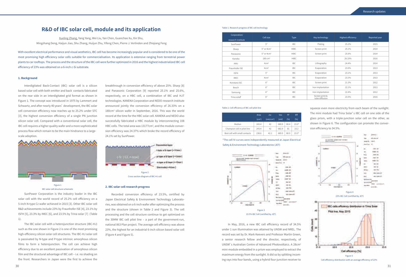
R&D of IBC solar cell, module and its applicationXueling Zhang, Yang Yang, Wei Liu, Yan Chen, Guanchao Xu, Xin Shu,
Mingzhang Deng, Haijun Jiao, Shu Zhang, Huijun Zhu, Yifeng Chen, Pierre J. Verlinden and Zhiqiang Feng
With excellent electrical performance and visual aesthetics, IBC cell has become increasingly popular and is considered to be one of the
most promising high efficiency solar cells suitable for commercialisation. Its application is extensive ranging from terrestrial power
plants to car rooftops. The process and the structure of the IBC cell were further optimized in 2016 and the highest industrialized IBC cell
efficiency of 23% was obtained on a 6-inch c-Si substrate.
3130
Interdigitated Back-Contact (IBC) solar cell is a silicon
based solar cell with both emitter and back contacts fabricated
on the rear side in an interdigitated grid format as shown in
Figure 1. The concept was introduced in 1975 by Lammert and
Schwartz, and after nearly 40 years’ development, the IBC solar
cell conversion efficiency now reaches up to 25.2% under STC
[3], the highest conversion efficiency of a single PN junction
silicon solar cell. Compared with a conventional solar cell, the
IBC cell requires a higher quality wafer and a more sophisticated
process flow which remain to be the main hindrance to a large-
scale adoption.
SunPower Corporation is the industry leader in the IBC
solar cell with the world record of 25.2% cell efficiency on a
5-inch N-type Cz wafer achieved in 2015 [3]. Other IBC solar cell
R&D achievements include 23% by Fraunhofer ISE [4], 23.1% by
ISFH [5], 23.3% by IMEC [6], and 23.5% by Trina solar [7] (Table
1).
The IBC solar cell with a heterojunction structure (IBC-HJ)
such as the one shown in Figure 2 is one of the most promising
high-efficiency silicon solar cell structures. The IBC-HJ solar cell
is passivated by N-type and P-type intrinsic amorphous silicon
films to form a heterojunction. The cell can achieve high
efficiency due to an excellent passivation of amorphous silicon
film and the structural advantage of IBC cell ‒ i.e. no shading on
the front. Researchers in Japan were the first to achieve the
breakthrough in conversion efficiency of above 25%. Sharp [8]
and Panasonic Corporation [9] reported 25.1% and 25.6%,
respectively, on a HBC cell, a combination of IBC and HJT
technologies. KANEKA Corporation and NEDO research institute
announced jointly the conversion efficiency of 26.33% on a
180cm2 silicon wafer in September, 2016. This was the world
record at the time for the HBC solar cell. KANEKA and NEDO also
successfully fabricated a HBC module by interconnecting 108
HBC cells. The total area was 13177cm2, and the module conver-
sion efficiency was 24.37% which broke the record efficiency of
24.1% set by SunPower.
In May, 2016, a new IBC cell efficiency record of 34.5%
under 1 sun illumination was attained by UNSW and NREL. The
record was set by Dr. Mark Keevers and Professor Martin Green,
a senior research fellow and the director, respectively, of
UNSW’s Australian Centre of Advanced Photovoltaics. A 28cm2
mini-module embedded in a prism was employed to extract the
maximum energy from the sunlight. It did so by splitting incom-
ing rays into four bands, using a hybrid four-junction receiver to
squeeze even more electricity from each beam of the sunlight.
The mini module had Trina Solar’s IBC cell on one side of the
glass prism, with a triple-junction solar cell on the other, as
shown in Figure 6. The configuration can promote the conver-
sion efficiency to 34.5%.
1. Background
Recorded conversion efficiency of 23.5%, certified by
Japan Electrical Safety & Environment Technology Laborato-
ries, was obtained on a 6-inch wafer after optimizing the process
and the structure (shown in Table 2 and Figure 3). The cell
processing and the cell structure continue to get optimized on
the 30MW IBC cell pilot line ‒ a part of the government-run,
national 863 Plan project. The average cell efficiency was above
23%, the highest for an industrial 6-inch silicon based solar cell
(Figure 4 and Figure 5).
2. IBC solar cell research progress
Research updates
Figure 1
IBC solar cell structure schematic
Figure 2
Cross section diagram of IBC-HJ cell
Figure 3
23.5% IBC Cell (certified by JET)
Figure 4
23% IBC Cell (certified by JET)
Figure 5
Cell efficiency distribution with an average efficiency of 23%
Corporation/
research institute Cell size
SunPower
Sharp
Panasonic
Kaneka
ANU
Fraunhofer ISE
ISFH
IMEC
Konstanz ISC
Bosch
Samsung
Trina solar
5"
5" or 4cm2
5" or 4cm2
180 cm2
4cm2
4cm2
5"
4cm2
6"
6"
6"
6"
IBC
HIBC
HIBC
HIBC
IBC
IBC
IBC
IBC
IBC
IBC
IBC
IBC
25.2%
25.1%
25.6%
26.33%
24.4%
23.0%
23.1%
23.3%
21.3%
22.1%
22.4%
23.5%
Type
Plating
Screen print
Screen print
Lithography
Evaporation
Evaporation
Evaporation
Screen print
Iron implantation
Iron implantation
Screen print & tube diffusion
2015
2014
2014
2016
2014
2013
2013
2013
2012
2013
2012
2016
Key technology Highest efficiency Reported year
Table 1. Research progress of IBC cell technology
Table 2. Cell efficiency of IBC cell pilot line
Area
(cm2) (mA/cm2) (mV) (%) (%)
Jsc Voc FF Eff
Median
Champion cell in pilot line
Best cell with small contacts
243.4
243.4
238.6
42
42
42.1
680.9
682.9
689.9
80.4
81
80.9
23.0*
23.2
23.5*
*The cell IV-curves were independently measured at Japan Electrical
Safety & Environment Technology Laboratories (JET)
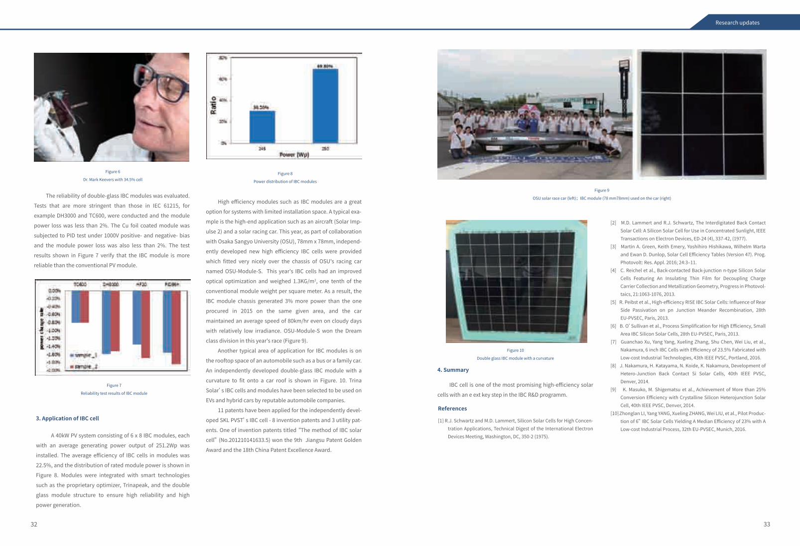
3332
SunPower Corporation is the industry leader in the IBC
solar cell with the world record of 25.2% cell efficiency on a
5-inch N-type Cz wafer achieved in 2015 [3]. Other IBC solar cell
R&D achievements include 23% by Fraunhofer ISE [4], 23.1% by
ISFH [5], 23.3% by IMEC [6], and 23.5% by Trina solar [7] (Table
1).
The IBC solar cell with a heterojunction structure (IBC-HJ)
such as the one shown in Figure 2 is one of the most promising
high-efficiency silicon solar cell structures. The IBC-HJ solar cell
is passivated by N-type and P-type intrinsic amorphous silicon
films to form a heterojunction. The cell can achieve high
efficiency due to an excellent passivation of amorphous silicon
film and the structural advantage of IBC cell ‒ i.e. no shading on
the front. Researchers in Japan were the first to achieve the
The reliability of double-glass IBC modules was evaluated.
Tests that are more stringent than those in IEC 61215, for
example DH3000 and TC600, were conducted and the module
power loss was less than 2%. The Cu foil coated module was
subjected to PID test under 1000V positive- and negative- bias
and the module power loss was also less than 2%. The test
results shown in Figure 7 verify that the IBC module is more
reliable than the conventional PV module.
IBC cell is one of the most promising high-efficiency solar
cells with an e ext key step in the IBC R&D programm.
High efficiency modules such as IBC modules are a great
option for systems with limited installation space. A typical exa-
mple is the high-end application such as an aircraft (Solar Imp-
ulse 2) and a solar racing car. This year, as part of collaboration
with Osaka Sangyo University (OSU), 78mm x 78mm, independ-
ently developed new high efficiency IBC cells were provided
which fitted very nicely over the chassis of OSU's racing car
named OSU-Module-S. This year's IBC cells had an improved
optical optimization and weighed 1.3KG/m2, one tenth of the
conventional module weight per square meter. As a result, the
IBC module chassis generated 3% more power than the one
procured in 2015 on the same given area, and the car
maintained an average speed of 80km/hr even on cloudy days
with relatively low irradiance. OSU-Module-S won the Dream
class division in this year's race (Figure 9).
Another typical area of application for IBC modules is on
the rooftop space of an automobile such as a bus or a family car.
An independently developed double-glass IBC module with a
curvature to fit onto a car roof is shown in Figure. 10. Trina
Solar’s IBC cells and modules have been selected to be used on
EVs and hybrid cars by reputable automobile companies.
11 patents have been applied for the independently devel-
oped SKL PVST’s IBC cell - 8 invention patents and 3 utility pat-
ents. One of invention patents titled “The method of IBC solar
cell” (No.201210141633.5) won the 9th Jiangsu Patent Golden
Award and the 18th China Patent Excellence Award.
4. Summary
Research updates
Figure 7
Reliability test results of IBC module
Figure 8
Power distribution of IBC modules
Figure 9
OSU solar race car (left);IBC module (78 mm78mm) used on the car (right)
Figure 10
Double glass IBC module with a curvature
Figure 6
Dr. Mark Keevers with 34.5% cell
[2] M.D. Lammert and R.J. Schwartz, The Interdigitated Back Contact Solar Cell: A Silicon Solar Cell for Use in Concentrated Sunlight, IEEE Transactions on Electron Devices, ED-24 (4), 337-42, (1977).
[3] Martin A. Green, Keith Emery, Yoshihiro Hishikawa, Wilhelm Warta and Ewan D. Dunlop, Solar Cell Efficiency Tables (Version 47). Prog. Photovolt: Res. Appl. 2016; 24:3‒11.
[4] C. Reichel et al., Back-contacted Back-junction n-type Silicon Solar Cells Featuring An Insulating Thin Film for Decoupling Charge Carrier Collection and Metallization Geometry, Progress in Photovol-taics, 21:1063-1076, 2013.
[5] R. Peibst et al., High-efficiency RISE IBC Solar Cells: Influence of Rear Side Passivation on pn Junction Meander Recombination, 28th EU-PVSEC, Paris, 2013.
[6] B. O’Sullivan et al., Process Simplification for High Efficiency, Small Area IBC Silicon Solar Cells, 28th EU-PVSEC, Paris, 2013.
[7] Guanchao Xu, Yang Yang, Xueling Zhang, Shu Chen, Wei Liu, et al., Nakamura, 6 inch IBC Cells with Efficiency of 23.5% Fabricated with Low-cost Industrial Technologies, 43th IEEE PVSC, Portland, 2016.
[8] J. Nakamura, H. Katayama, N. Koide, K. Nakamura, Development of Hetero-Junction Back Contact Si Solar Cells, 40th IEEE PVSC, Denver, 2014.
[9] K. Masuko, M. Shigematsu et al., Achievement of More than 25% Conversion Efficiency with Crystalline Silicon Heterojunction Solar Cell, 40th IEEE PVSC, Denver, 2014.
[10] Zhonglan LI, Yang YANG, Xueling ZHANG, Wei LIU, et al., Pilot Produc-tion of 6” IBC Solar Cells Yielding A Median Efficiency of 23% with A Low-cost Industrial Process, 32th EU-PVSEC, Munich, 2016.
References
[1] R.J. Schwartz and M.D. Lammert, Silicon Solar Cells for High Concen-tration Applications, Technical Digest of the International Electron Devices Meeting, Washington, DC, 350-2 (1975).
3. Application of IBC cell
A 40kW PV system consisting of 6 x 8 IBC modules, each
with an average generating power output of 251.2Wp was
installed. The average efficiency of IBC cells in modules was
22.5%, and the distribution of rated module power is shown in
Figure 8. Modules were integrated with smart technologies
such as the proprietary optimizer, Trinapeak, and the double
glass module structure to ensure high reliability and high
power generation.
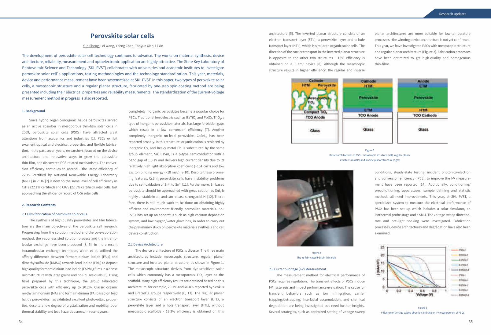
Figure 1
Device architectures of PSCs: mesoscopic structure (left), regular planar
structure (middle) and inverse planar structure (right)
Figure 3
Influence of voltage sweep direction and rate on I-V measurement of PSCs
Figure 2
The as-fabricated PSCs in Trina lab
2.3 Current-voltage (I-V) Measurement
The measurement method for electrical performance of
PSCs requires regulation. The transient effects of PSCs induce
I-V hysteresis and impact performance evaluation. The cause for
transient behaviors such as ion immigration, carrier
trapping/detrapping, interfacial accumulation, and chemical
degradation are being investigated but need further insights.
Several strategies, such as optimized setting of voltage sweep
conditions, steady-state testing, incident photon-to-electron
and conversion efficiency (IPCE), to improve the I-V measure-
ment have been reported [14]. Additionally, conditioning/
preconditioning, apparatuses, sample defining and statistic
methods all need improvements. This year, at SKL PVST, a
specialized system to measure the electrical performance of
PSCs has been set up which includes a solar simulator, an
isothermal probe stage and a SMU. The voltage sweep direction,
rate and pre-light soaking were investigated. Fabrication
processes, device architectures and degradation have also been
examined.
architecture [5]. The inverted planar structure consists of an
electron transport layer (ETL), a perovskite layer and a hole
transport layer (HTL), which is similar to organic solar cells. The
direction of the carrier transport in the inverted planar structure
is opposite to the other two structures - 15% efficiency is
obtained on a 1 cm2 device [8]. Although the mesoscopic
structure results in higher efficiency, the regular and inverse
planar architectures are more suitable for low-temperature
processes - the winning device architecture is not yet confirmed.
This year, we have investigated PSCs with mesoscopic structure
and regular planar architecture (Figure 2). Fabrication processes
have been optimized to get high-quality and homogenous
thin-films.
Since hybrid organic-inorganic halide perovskites served
as an active absorber in mesoporous thin-film solar cells in
2009, perovskite solar cells (PSCs) have attracted great
attentions from academics and industries [1]. PSCs exhibit
excellent optical and electrical properties, and flexible fabrica-
tion. In the past seven years, researchers focused on the device
architecture and innovative ways to grow the perovskite
thin-film, and discovered PCS-related mechanisms. The conver-
sion efficiency continues to ascend - the latest efficiency of
22.1% certified by National Renewable Energy Laboratory
(NREL) in 2016 [2] is now on the same level of cell efficiency as
CdTe (22.1% certified) and CIGS (22.3% certified) solar cells, fast
approaching the efficiency record of C-Si solar cells.
1. Background
2. Research Contents
3534
Perovskite solar cellsYun Sheng, Lei Wang, Yifeng Chen, Taoyun Xiao, Li Yin
The development of perovskite solar cell technology continues to advance. The works on material synthesis, device architecture, reliability, measurement and optoelectronic application are highly attractive. The State Key Laboratory of Photovoltaic Science and Technology (SKL PVST) collaborates with universities and academic institutes to investigate perovskite solar cell’s applications, testing methodologies and the technology standardization. This year, materials, device and performance measurement have been systematized at SKL PVST. In this paper, two types of perovskite solar cells, a mesoscopic structure and a regular planar structure, fabricated by one-step spin-coating method are being presented including their electrical properties and reliability measurements. The standardization of the current-voltage measurement method in progress is also reported.
Research updates
References
[1] R.J. Schwartz and M.D. Lammert, Silicon Solar Cells for High Concen-tration Applications, Technical Digest of the International Electron Devices Meeting, Washington, DC, 350-2 (1975).
2.1 Film fabrication of perovskite solar cells
The synthesis of high quality perovskites and film fabrica-
tion are the main objectives of the perovskite cell research.
Progressing from the solution method and the co-evaporation
method, the vapor-assisted solution process and the intramo-
lecular exchange have been proposed [3, 5]. In more recent
intramolecular exchange technique, Woon et al. utilized the
affinity difference between formamidinium iodide (FAIs) and
dimethylsulfoxide (DMSO) towards lead iodide (PbI2) to deposit
high quality formamidinium lead iodide (FAPbI3) films in a dense
microstructure with large grains and no PbI2 residuals [6]. Using
films prepared by this technique, the group fabricated
perovsikte cells with efficiency up to 20.2%. Classic organic
methylammonium (MA) and formamidinium (FA) based on lead
halide perovskites has exhibited excellent photovoltaic proper-
ties, despite a low degree of crystallization and mobility, poor
thermal stability and lead hazardousness. In recent years,
2.2 Device Architecture
The device architecture of PSCs is diverse. The three main
architectures include mesoscopic structure, regular planar
structure and inverted planar structure, as shown in Figure 1.
The mesoscopic structure derives from dye-sensitized solar
cells which commonly has a mesoporous TiO2 layer as the
scaffold. Many high efficiency results are obtained based on this
architecture, for example, 20.1% and 20.8% reported by Seok’s
and Gratzel’s groups respectively [6, 13]. The regular planar
structure consists of an electron transport layer (ETL), a
perovskite layer and a hole transport layer (HTL), without
mesoscopic scaffolds - 19.3% efficiency is obtained on this
completely inorganic perovskites became a popular choice for
PSCs. Traditional ferroelectric such as BaTiO3 and Pb(Zr, Ti)O3, a
type of inorganic perovskite materials, has large forbidden gaps
which result in a low conversion efficiency [7]. Another
completely inorganic no-lead perovskite, CsSnI3, has been
reported broadly. In this structure, organic cation is replaced by
inorganic Cs, and heavy metal Pb is substituted by the same
group element, Sn. CsSnI3 is a p-type semiconductor with a
band gap of 1.3 eV and delivers high current density due to its
relatively high light absorption coefficient (~104 cm-1) and low
exciton binding energy (~18 meV) [8-10]. Despite these promis-
ing features, CsSnI3 perovskite cells have instability problems
due to self-oxidation of Sn2+ to Sn4+ [11]. Furthermore, Sn based
perovskite should be approached with great caution as SnI2 is
highly unstable in air, and can release strong acid, HI [12]. There-
fore, there is still much work to be done on obtaining highly
efficient and environment friendly perovskite materials. SKL
PVST has set up an apparatus such as high vacuum deposition
system, and low oxygen/water glove box, in order to carry out
the preliminary study on perovskite materials synthesis and cell
device construction.
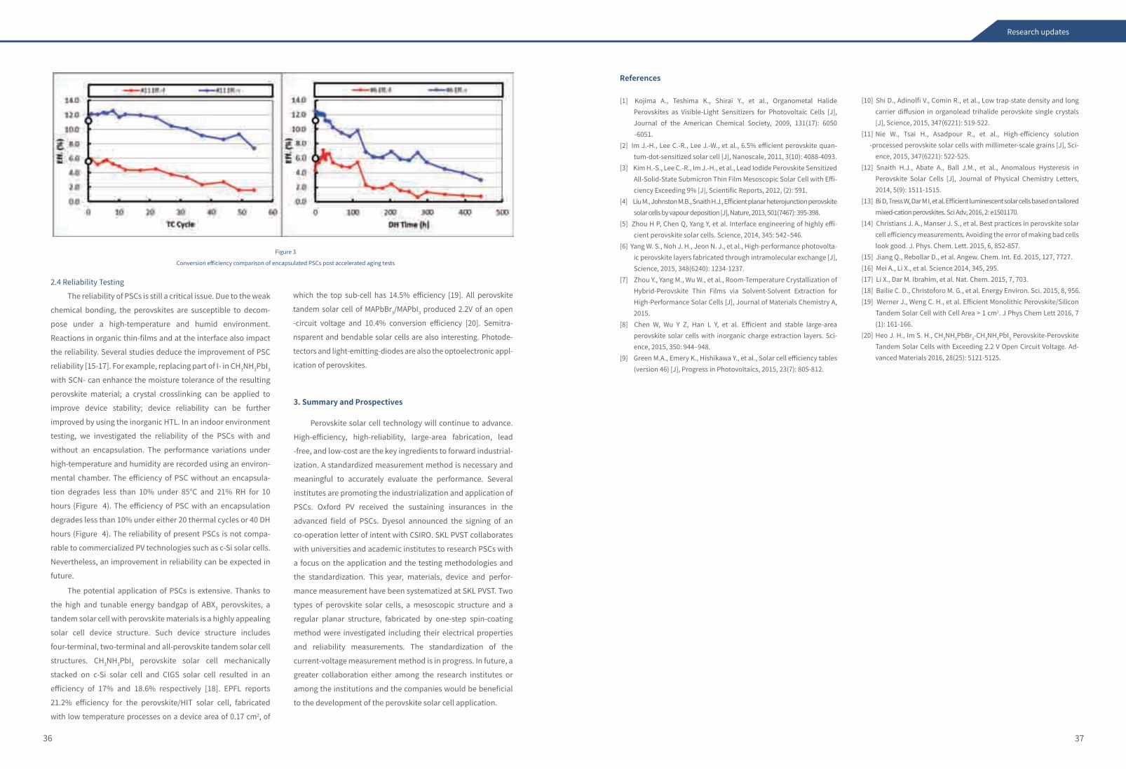
References
[1] Kojima A., Teshima K., Shirai Y., et al., Organometal Halide Perovskites as Visible-Light Sensitizers for Photovoltaic Cells [J], Journal of the American Chemical Society, 2009, 131(17): 6050
-6051.[2] Im J.-H., Lee C.-R., Lee J.-W., et al., 6.5% efficient perovskite quan-
tum-dot-sensitized solar cell [J], Nanoscale, 2011, 3(10): 4088-4093.[3] Kim H.-S., Lee C.-R., Im J.-H., et al., Lead Iodide Perovskite Sensitized
All-Solid-State Submicron Thin Film Mesoscopic Solar Cell with Effi-ciency Exceeding 9% [J], Scientific Reports, 2012, (2): 591.
[4] Liu M., Johnston M.B., Snaith H.J., Efficient planar heterojunction perovskite solar cells by vapour deposition [J], Nature, 2013, 501(7467): 395-398.
[5] Zhou H P, Chen Q, Yang Y, et al. Interface engineering of highly effi-cient perovskite solar cells. Science, 2014, 345: 542‒546.
[6] Yang W. S., Noh J. H., Jeon N. J., et al., High-performance photovolta-ic perovskite layers fabricated through intramolecular exchange [J], Science, 2015, 348(6240): 1234-1237.
[7] Zhou Y., Yang M., Wu W., et al., Room-Temperature Crystallization of Hybrid-Perovskite Thin Films via Solvent-Solvent Extraction for High-Performance Solar Cells [J], Journal of Materials Chemistry A, 2015.
[8] Chen W, Wu Y Z, Han L Y, et al. Efficient and stable large-area perovskite solar cells with inorganic charge extraction layers. Sci-ence, 2015, 350: 944‒948.
[9] Green M.A., Emery K., Hishikawa Y., et al., Solar cell efficiency tables (version 46) [J], Progress in Photovoltaics, 2015, 23(7): 805-812.
[10] Shi D., Adinolfi V., Comin R., et al., Low trap-state density and long carrier diffusion in organolead trihalide perovskite single crystals [J], Science, 2015, 347(6221): 519-522.
[11] Nie W., Tsai H., Asadpour R., et al., High-efficiency solution -processed perovskite solar cells with millimeter-scale grains [J], Sci-
ence, 2015, 347(6221): 522-525.[12] Snaith H.J., Abate A., Ball J.M., et al., Anomalous Hysteresis in
Perovskite Solar Cells [J], Journal of Physical Chemistry Letters, 2014, 5(9): 1511-1515.
[13] Bi D, Tress W, Dar M I, et al. Efficient luminescent solar cells based on tailored mixed-cation perovskites. Sci Adv, 2016, 2: e1501170.
[14] Christians J. A., Manser J. S., et al. Best practices in perovskite solar cell efficiency measurements. Avoiding the error of making bad cells look good. J. Phys. Chem. Lett. 2015, 6, 852-857.
[15] Jiang Q., Rebollar D., et al. Angew. Chem. Int. Ed. 2015, 127, 7727.[16] Mei A., Li X., et al. Science 2014, 345, 295.[17] Li X., Dar M. Ibrahim, et al. Nat. Chem. 2015, 7, 703.[18] Bailie C. D., Christoforo M. G., et al. Energy Environ. Sci. 2015, 8, 956.[19] Werner J., Weng C. H., et al. Efficient Monolithic Perovskite/Silicon
Tandem Solar Cell with Cell Area > 1 cm2. J Phys Chem Lett 2016, 7(1): 161-166.
[20] Heo J. H., Im S. H., CH3NH3PbBr3-CH3NH3PbI3 Perovskite-Perovskite Tandem Solar Cells with Exceeding 2.2 V Open Circuit Voltage. Ad-vanced Materials 2016, 28(25): 5121-5125.
3736
Perovskite solar cell technology will continue to advance.
High-efficiency, high-reliability, large-area fabrication, lead
-free, and low-cost are the key ingredients to forward industrial-
ization. A standardized measurement method is necessary and
meaningful to accurately evaluate the performance. Several
institutes are promoting the industrialization and application of
PSCs. Oxford PV received the sustaining insurances in the
advanced field of PSCs. Dyesol announced the signing of an
co-operation letter of intent with CSIRO. SKL PVST collaborates
with universities and academic institutes to research PSCs with
a focus on the application and the testing methodologies and
the standardization. This year, materials, device and perfor-
mance measurement have been systematized at SKL PVST. Two
types of perovskite solar cells, a mesoscopic structure and a
regular planar structure, fabricated by one-step spin-coating
method were investigated including their electrical properties
and reliability measurements. The standardization of the
current-voltage measurement method is in progress. In future, a
greater collaboration either among the research institutes or
among the institutions and the companies would be beneficial
to the development of the perovskite solar cell application.
3. Summary and Prospectives
Research updates
Figure 3
Conversion efficiency comparison of encapsulated PSCs post accelerated aging tests
2.4 Reliability Testing
The reliability of PSCs is still a critical issue. Due to the weak
chemical bonding, the perovskites are susceptible to decom-
pose under a high-temperature and humid environment.
Reactions in organic thin-films and at the interface also impact
the reliability. Several studies deduce the improvement of PSC
reliability [15-17]. For example, replacing part of I- in CH3NH3PbI3
with SCN- can enhance the moisture tolerance of the resulting
perovskite material; a crystal crosslinking can be applied to
improve device stability; device reliability can be further
improved by using the inorganic HTL. In an indoor environment
testing, we investigated the reliability of the PSCs with and
without an encapsulation. The performance variations under
high-temperature and humidity are recorded using an environ-
mental chamber. The efficiency of PSC without an encapsula-
tion degrades less than 10% under 85℃ and 21% RH for 10
hours (Figure 4). The efficiency of PSC with an encapsulation
degrades less than 10% under either 20 thermal cycles or 40 DH
hours (Figure 4). The reliability of present PSCs is not compa-
rable to commercialized PV technologies such as c-Si solar cells.
Nevertheless, an improvement in reliability can be expected in
future.
The potential application of PSCs is extensive. Thanks to
the high and tunable energy bandgap of ABX3 perovskites, a
tandem solar cell with perovskite materials is a highly appealing
solar cell device structure. Such device structure includes
four-terminal, two-terminal and all-perovskite tandem solar cell
structures. CH3NH3PbI3 perovskite solar cell mechanically
stacked on c-Si solar cell and CIGS solar cell resulted in an
efficiency of 17% and 18.6% respectively [18]. EPFL reports
21.2% efficiency for the perovskite/HIT solar cell, fabricated
with low temperature processes on a device area of 0.17 cm2, of
which the top sub-cell has 14.5% efficiency [19]. All perovskite
tandem solar cell of MAPbBr3/MAPbI3 produced 2.2V of an open
-circuit voltage and 10.4% conversion efficiency [20]. Semitra-
nsparent and bendable solar cells are also interesting. Photode-
tectors and light-emitting-diodes are also the optoelectronic appl-
ication of perovskites.
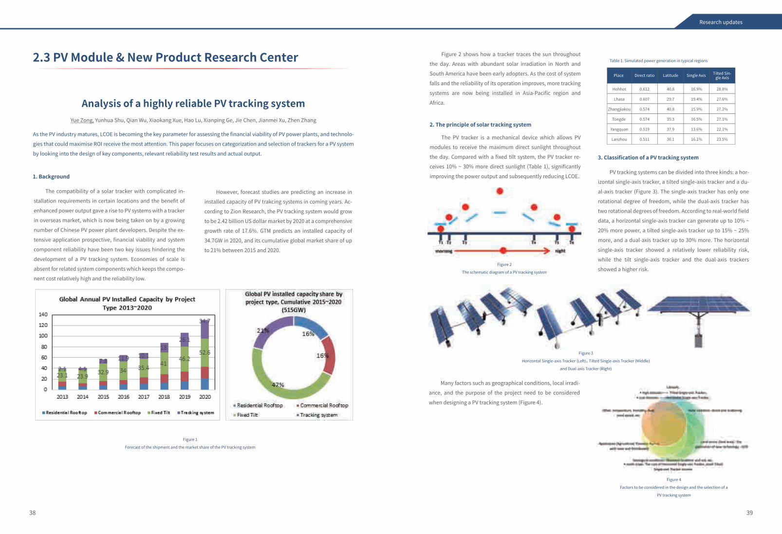
The PV tracker is a mechanical device which allows PV
modules to receive the maximum direct sunlight throughout
the day. Compared with a fixed tilt system, the PV tracker re-
ceives 10% ~ 30% more direct sunlight (Table 1), significantly
improving the power output and subsequently reducing LCOE.
2. The principle of solar tracking system
PV tracking systems can be divided into three kinds: a hor-
izontal single-axis tracker, a tilted single-axis tracker and a du-
al-axis tracker (Figure 3). The single-axis tracker has only one
rotational degree of freedom, while the dual-axis tracker has
two rotational degrees of freedom. According to real-world field
data, a horizontal single-axis tracker can generate up to 10% ~
20% more power, a tilted single-axis tracker up to 15% ~ 25%
more, and a dual-axis tracker up to 30% more. The horizontal
single-axis tracker showed a relatively lower reliability risk,
while the tilt single-axis tracker and the dual-axis trackers
showed a higher risk.
Many factors such as geographical conditions, local irradi-
ance, and the purpose of the project need to be considered
when designing a PV tracking system (Figure 4).
3. Classification of a PV tracking system
Figure 3
Horizontal Single-axis Tracker (Left), Tilted Single-axis Tracker (Middle)
and Dual-axis Tracker (Right)
Figure 4
Factors to be considered in the design and the selection of a
PV tracking system
Figure 2 shows how a tracker traces the sun throughout
the day. Areas with abundant solar irradiation in North and
South America have been early adopters. As the cost of system
falls and the reliability of its operation improves, more tracking
systems are now being installed in Asia-Pacific region and
Africa.
Figure 2
The schematic diagram of a PV tracking system
Place Direct ratio Latitude Tilted Sin-gle AxisSingle Axis
Hohhot
Lhasa
Zhangjiakou
Tongde
Yangquan
Lanzhou
0.612
0.607
0.574
0.574
0.519
0.511
40.8
29.7
40.8
35.3
37.9
36.1
16.9%
19.4%
15.9%
16.5%
13.6%
16.1%
28.8%
27.6%
27.2%
27.1%
22.1%
23.5%
Table 1. Simulated power generation in typical regions
38 39
As the PV industry matures, LCOE is becoming the key parameter for assessing the financial viability of PV power plants, and technolo-
gies that could maximise ROI receive the most attention. This paper focuses on categorization and selection of trackers for a PV system
by looking into the design of key components, relevant reliability test results and actual output.
Analysis of a highly reliable PV tracking systemYue Zong, Yunhua Shu, Qian Wu, Xiaokang Xue, Hao Lu, Xianping Ge, Jie Chen, Jianmei Xu, Zhen Zhang
2.3 PV Module & New Product Research Center
Research updates
The compatibility of a solar tracker with complicated in-
stallation requirements in certain locations and the benefit of
enhanced power output gave a rise to PV systems with a tracker
in overseas market, which is now being taken on by a growing
number of Chinese PV power plant developers. Despite the ex-
tensive application prospective, financial viability and system
component reliability have been two key issues hindering the
development of a PV tracking system. Economies of scale is
absent for related system components which keeps the compo-
nent cost relatively high and the reliability low.
1. Background
Figure 1
Forecast of the shipment and the market share of the PV tracking system
However, forecast studies are predicting an increase in
installed capacity of PV trakcing systems in coming years. Ac-
cording to Zion Research, the PV tracking system would grow
to be 2.42 billion US dollar market by 2020 at a comprehensive
growth rate of 17.6%. GTM predicts an installed capacity of
34.7GW in 2020, and its cumulative global market share of up
to 21% between 2015 and 2020.
IEC 61215, the most authoritative standard in the PV indus-
try, is not suitable to verify the durability of PV modules over war-
ranted lifetime which has recently changed from 20 years to 25
years. Durability is the module’s ability to withstand the long-
term degradation, affected by a combination of environmental
factors, not just one.
Based on the Koppen climate classification, climates for PV
module installations can be divided into four categories - hot-hu-
midity, hot-dry, temperate, cold and alpine [1]. Key environmen-
tal factors vary greatly from one climatic region to another [2]. N.
C. Park et al. simulated the climate condition in terms of temper-
ature and moisture using Eyring and Peck models. 1000hr damp
heat (DH, 85 ℃,85% R.H.) treatment was equivalent to an actual
module operation of 23 years in a hot-humid region, 40 years in a
hot-dry region, and 106 years in an alpine region [3]. The level of
UV also varied for each region. W. Herrmann et al. measured the
daily temperature variation of modules in all four climate regions
[4].
Figure 1 shows appearances of two five-year-old encapsu-
lated modules with the same backsheet in temperate and hot-
dry climates. Although both backsheets had been IEC 61215 cer-
tified by TUV Rheinland, it is clear that both backsheets degrad-
ed after fiver years of operation in field.
1. Introduction
Degradation modes and mechanisms for modules in differ-
ent climates were studied using the same brand (Siemens) mod-
ules installed in temperate and hot-dry regions for 23 years. All
modules were assembled with monocrystaline cells and Ted-
lar-PET-Tedlar (TPT) backsheets. The graph in Figure 2 demon-
strates that the fill factor (FF) degradation caused by an in-
creased series resistance (Rs) was the biggest contributor to-
wards the power degradation for modules in the temerpate cli-
mate, Shenzhen. Figure 3 shows infrared images of modules in
two regions with 8A passing through. Hot spots were observed
in the solder, and high temperature was detected in the finger
area which meant the welding between Ag busbar and Sn-Pb
alloy had degraded. The bonding strength between fingers and
the silicon substrate also became weaker due to the water vapor
ingress, the high temperature and the UV irradiation.
2. Module degradation mechanism after 23 years of exposu-re
Durability of modules in the field is attracting a growing attention in the PV industry. IEC standards are more effective for evaluating
modules’ short-term reliability than long-term durability. The degradation mechanism of modules in the field should be investigated
thoroughly, especially for harsh climates. Factors that influence the module power degradation in an actual operating condition are dif-
ferent from those observed in an indoor accelerated aging test laboratory. This paper investigates the power degradation mechanisms
in hot-humid and hot-dry regions with a series of accelerated aging tests in combination with ultraviolet irradiation.
Correlation of modules’ long-term reliability withindoor accelerated aging tests
Qiangzhong Zhu, Hui Shen, Zhichao Ji, Jing Mao, Quan Sun and Jianmei Xu
Figure 1
Comparative appearance study of the same type of modules after an
actual field operation of five years in a temperate region (left) and a
hot-dry region (right)
Figure 2
The electrical performance of modules after 23 years of operation in
Shenzhen and Dunhuang
40
Due to the market competing on price rather than on qual-
ity and reliability, numerous sub-standard products have been
introduced and created a doubt over viability of PV plants over
its assumed service lifetime of 25 years. Sicheng Wang, a Chi-
nese PV system expert, pointed out that the most effective way
to reduce LCOE is to employ a PV tracking system and resolve
the reliability problem that hinders extensive adoption of the
technology. In order to guarantee the maximum power genera-
tion over the lifetime of PV plants, developers would be re-
quired to select an optimal technology for the purpose of the
project, implement quality control measures in each phase of
the project development, and reduce cost by integrating a
smart system and component design, not by sourcing the
cheapest components.
A PV tracking system consists of four key components -
support rails, bearings, motors & gear reducer, and controller.
Three common failure modes are detailed below.
1) Motor failure: An environment with high humidity and
high temperature can accelerate the aging of insulation and the
formation of leakage current. Sand and moisture can penetrate
into the bearings and damage them, and overheat the motor.
2) Control system failure: the timing controlling system
was employed in the track-er.
3) Structure failure: Sinking land and slope cause rails to
deform over time which would eventually prevent the axis from
rotating. The core component of the rotating mechanism, the bearing, could fail. Inappropriate foundation design and poor
construction cause the system to fail.
Core components of the tracker should be tested in accor-
dance with UL2703 and UL3703 standards to ensure the reliabil-
ity and durability. Test items should include mechanical loading
test, salt fog test, dustproof and waterproof test, grounding
continuity test, and a series of environmental aging tests such
as thermal cycling, damp and hot, and UV resistance (Table 2).
4. Raliability analysis of PV tracking system
For a PV market which favors cost-effective smart PV sys-
tems, a PV tracker system should be considered. The recent
trends for the PV tracker systems are 1) adoption of high-effi-
ciency bifocal solar cells to increase the power generation and
to reduce LCOE; 2) adoption of best MPPT tracker with smart
controller chips to realize a maximum power generation; 3)
adoption of the cloud platform to smartly manage the PV power
plants.
5. Summary and perspectives References
[1] Sun yinyin, BaoJianBin, Wang fang. Researches on the automatic sun tracker. Mechanical design and manufacturing, 2005.
[2] Soteris Kaloglrou. The Potential of Solar Industrial Process Heat Ap-plications. Applied Energy, 2003, 337~361.
[3] Ai.B. Calculation of the Hourly and Daily Radiation Incident on Three Step Tracking Planes. Energy Conversion and Management, 2003, 44: 1999-2011.
[4] G. Martin. Renewable Energy Gets the Green Light in Chicago. Power and Energy Magazine, 2003. 34~39.
41
Research updates
Table 2. Reliability tests for key components of a PV tracking system
No. Parts name Test Item
1
2
3
Rail fasteners
Motor reducer
Control box
1.GB/T 10125-2012 corrosion test, salt fog test2.IEC 61701-2011 PV modules salt spray corrosion test
1.IEC 61215-2005 2.GB/ T 12665-2008 3.GB/ T 1311-2008 4.GB 4208-2008 (IP)5.UL 50E-2007
1.GB 4208-2008 (IP)2.GB/ T 2423.17-20083.GB/ T 2423.1-20084.GB/ T 2423.2-20015.GB/ T 2423.34-2012
Anti-corrosion ability of rails & fasteners
Environmental aging test; Protection grade test;Metal surface corrosion resistant test
Environmental aging test; Protection grade test;Metal surface corrosion
resistant test
Reference standard
The power degradation mechanism of modules in the hot-
humid region and the hot-dry region are different due to varying
amounts of moisture, acid and sand. In the hot-humid region,
the moisture ingress could accelerate the release of acetate acid
as EVA decomposes and subsequently degrades the welding
strength in the module. The main indoor accelerated aging test
is the damp heat test, which is not an effective evaluation tool to
assess the degradation of modules in field, mainly due to a lack
4. Conclusion
The metallographic cross-sectional images in Figure 8 indi-
cate that the presence of acetate acid exerts great influence on
the growth rate of Ag3Sn. The Ag layer in the module with high
VA content was almost replaced by Ag3Sn - the thickness of
Ag3Sn was 13μm compared to 6μm in the module with low VA
content ‒ affirming that acetate acid does accelerate the growth
of Ag3Sn alloy layer.
Figure 7
Metallographic cross-sectional images of solar modules
encapsulated with varying degrees of VA content
Figure 8
Temperature ramp rate under TC and TS test for modules
of different types
3.2 Thermal shock (TS) test
A combination of high temperature and acetate acid seems
to accelerate the growth of alloyed soldering layer, and decrease
the welding strength. It also seems that a large amount of stress
damages accumulate on the module due to the mismatch of
thermal expansion coefficients of Si and Cu. The module
damage caused by temperature variation in the field could be
simulated by Thermal Cycle (TC) test described in IEC 61215.
However to more accurately simulate the temperature variation
on the field, Thermal Shock (TS) test was conducted.
When clouds cover a module, the irradiation on the module
drops dramatically. The module temperature could be de-
scribed by equation (2). Please note that in order to simplify the
model, the diffused light has been ignored:
(2)
where is the module temperature at time of t, is
the temperature variation within time range,Q is the heat
flowing out the module within time range, m is the mass of
the module, c is module’s heat capacity, T1 is the environment
temperature, R is the module heat resistance.
Equation (2) could be expressed as equation (3):
(3)
Equation (4) is obtained by integrating equation (3)
(4)
Considering the boundary condition of the module tem-
perature of T0 at t=0,
(5)
When cloud shadow moves away from the module surface,
the module temperature can be expressed by Equation (6):
(6)
where E is the energy absorbed by the module.
From these equations above, we could deduce that the
module temperature ramp rate is related to the heat resistance,
the module mass and the heat capacity. In TC test, the module
temperature could be described as equation (7).
(7)
where k is the ramp rate of the environmental chamber,
and should be less than 100℃/h described in IEC 61215. By solv-
ing equation (7), we obtain equation (8):
(8)
The ramp rate could be written as:
(9)
According to the equation (9), the temperate ramp rate for
different types of modules is strongly correlated with the tem-
perature ramp rate of the environmental chamber. The temper-
ature of dual glass modules and conventional modules under TS
test and TC test were measured (Figure 8).
42
Research updates
43
3. Indoor accelerated aging test
For modules in the hot-dry climate, Dunhuang, the short-
circuit current (Isc) degradation due to the abrasion of the glass
was the biggest contributing factor to the power degradation
(Figure 4). Some FF degradation due to cell cracks was also no-
ticeable. It is inferred that cell cracks were caused by the wind
in Dunhuang.
The cause of Rs increase in modules in Shenzhen was in-
vestigated by comparing metallographic cross-sectional images
of modules in both places as shown in Figure 5. Cracks seemed
to appear in Shenzhen modules’ welding spots. Cracks were
caused by the weakening welding strength ‒ to verify the thick-
ness of Ag3Sn alloy in modules from both places were compared.
The thickness of Ag3Sn alloy could be estimated by diffusion dy-
namics equation below [5]:
As the above equation states, the thickness of Ag3Sn is af-
fected by the temperature, the time, and the reaction energy.
Any thickness difference may have been due to the formation of
acetate acid from the degraded EVA and the moisture ingress
which decreased the reaction energy. In order to demonstrate
this, modules encapsulated with EVA of different VA content
were fabricated, and the growth rate of alloy under highly accel-
erated stress test condition (HAST, 121℃+100% R.H.) was com-
pared.
where, d is the final alloy thickness, d0 is the initial thick-
ness, D0 is the diffusion constant, R is the gas constant, Ea is the
reaction activation energy between Ag and Sn, T is the absolute
temperature, and t is the dwell time at typical temperatures.
Figure 3
Infrared images of modules in Shenzhen and Dunhuang
measured with a current of 8A passing through
Figure 5
Metallographic cross-sectional images of PV modules in
Shenzhen and Dunhuang
Figure 6
Infrared images of solar modules encapsulated with
varying degrees of VA content after 596hour HAST test
Figure 4
EL images of the modules in Dunhuang (left) and
Shenzhen (right)
3.1 HAST test
EVAs with high VA and low VA content were used to demo-
nstrate the influence of acetate acid on the growth rate of Ag3Sn
- the encapsulated modules were subjected to the experiment
for 596 hours. Infrared images in Figure 6 illustrate that all weld-
ing spots in the module encapsulated with high VA content
failed, while only a few welding spots in the module with low VA
content failed.
(Equation.1)exp Ea( )
A full set of environmental tests in IEC61215 was carried out to analyze the bonding reliability of the silicone structural adhesive in in-
stalled solar modules. Additional non-standard tests were also carried out in simulated outdoor condition. The analysis verifies that the
silicone adhesive can ensure the safety and the reliability of PV modules over long term.
Reliability of silicone structural adhesive in PV moduleJing Mao, Hao Lu, Qiangzhong Zhu, Hui Shen, Yue Zong, Zhichao Ji
With increasing demand of PV generation, customers
expect higher quality and highly reliable PV products. Dual
-glass modules are designed for high reliability in harsh regions,
in particular, tropical, arid, marine and corrosive environments
[1]. Traditional way to attach a dual-glass module to the mou-
nting rail is to use 4 clamps. A new attachment method, “Gecko
grip”, is proposed where mounting rail hooks are glued to the
rear glass of the panel with silicone adhesive.
“Gecko grip” has the advantage of easy installation, high
reliability and high compatibility. The rail hook is glued to the
rear glass of the panel with silicone structure adhesive which is
mechanically strong and anti-aging. The mechanical properties
of silicone is known to be stable under ultraviolet light - Si-O
bond energy is about 420kJ/mol and 320nm UV energy is about
360kJ/mol. The silicone structural adhesive has been widely
used for more than 40 years in various fields such as buildings,
electronics and aerospace. The hook is made of aluminum
alloy, has a “cross-hole” design, which ensures an accurate and
fast installation, and can withstand the wind load capacity of a
dual-glass module. The hook is compatible with commonly
available brackets on the market.
kept in a water bath at 45℃ for 21 days. This test condition
was chosen to determine the properties of the silicon adhesive.
During the development stage of dual-glass modules with the
rear rail hook attached, stringency of the reliability test was in-
creased and the water temperature was raised to 55℃. The pass
criterion was set at 85% adhesion level or Cohesive Failure (CF)
after 21 days in the hot water bath. We selected two kinds of ad-
hesives from manufacturer A and manufacturer B. The adhesive
from manufacturer A lost adhesion to the glass after first 7 days
as shown in Figure 1(a), while the adhesive from manufacturer
B met the requirements and passed the hot water bath test
(55°C, 21 days) retaining 85% of CF area as shown in Figure 1(b).
The silicon adhesive of manufacturer B was selected for evalua-
tion in the following reliability test.
1. Background
Figure 1
(a) Adhesive from manufacturer A showed failure after HAST
test; (b) Adhesive from manufacturer B passed HAST test
Figure 2
(a) Pull and shear forces applied during the environmental test; (b) Degradation of the pull and shear strength post environmental tests
2. Environmental Reliability Test
2.1 Type selection of silicone adhesive
According to ETAG002.e [2], silicone bonded samples were
2.2 Conventional Environmental Test
Test samples were prepared to evaluate the mechanical
The power degradation mechanism of modules in the hot-
humid region and the hot-dry region are different due to varying
amounts of moisture, acid and sand. In the hot-humid region,
the moisture ingress could accelerate the release of acetate acid
as EVA decomposes and subsequently degrades the welding
strength in the module. The main indoor accelerated aging test
is the damp heat test, which is not an effective evaluation tool to
assess the degradation of modules in field, mainly due to a lack
of sequential qualification tests combined with UV and DH test.
The acetate acid could accelerate the weakening of weld-
ing strength by increasing the growth rate of Ag3Sn alloy. The
indoor accelerated aging test which could simulate the module
degradation in the hot-humid region is the damp heat test.
However the absence of UV light in the test results in underesti-
mating the amount of acid formation. Thus, the damp heat test
combined with UV light would be an appropriate method to
evaluate the durability of modules. The thermal stress related
failure could be simulated by the thermal cycle test, however,
the temperature ramp rate on different types of modules could
not be evaluated in this test. Introducing the thermal shock test
could assist in assessing the durability variance among different
types of modules.
15
4544
References
[1] TJ Phillips, CJW Bonfils, Köppen Bioclimatic Evaluation of CMIP His-torical Climate Simulations, Environmental Research Letters, 2015, 10, 064005.
[2] W. Hermann, N. Bogdanski, Outdoor Weathering of PV Modules-Ef-fects of Various Climates and Comparison with Accelerated Labora-tory Testing, 2011, IEEE, 11, 978-1-4244-9965-6.
[3] Park N. C., Oh W. W., and Kim D. H., Effect of Temperature and Humid-ity on the Degradation Rate of Multicrystalline Silicon Photovoltaic Module; International Journal of Photoenergy, 2013, 925280.
[4] Herrmann W., Bogdanski N., Reil F., Köhl M., Weiss K.-A., Assmus M., Heck M., PV Module Degradation Caused by Thermomechanical Stress: Real Impacts of Outdoor Weathering versus Accelerated Testing in the Laboratory, Reli-ability of Photovoltaic Cells, Modules, Components, and Systems III, 2010, 7773,77730I.
[5] WH Chen, CF Yu, HC Cheng, YM Tsai, ST Lu, IMC Growth Reaction and Its Ef-fects on Solder Joint Thermal Cycling Reliability of 3D Chip Stacking Packag-ing, Microelectronics Reliability, 2013, 53, 30-40.
晶体硅光伏技术研究成果Research updates
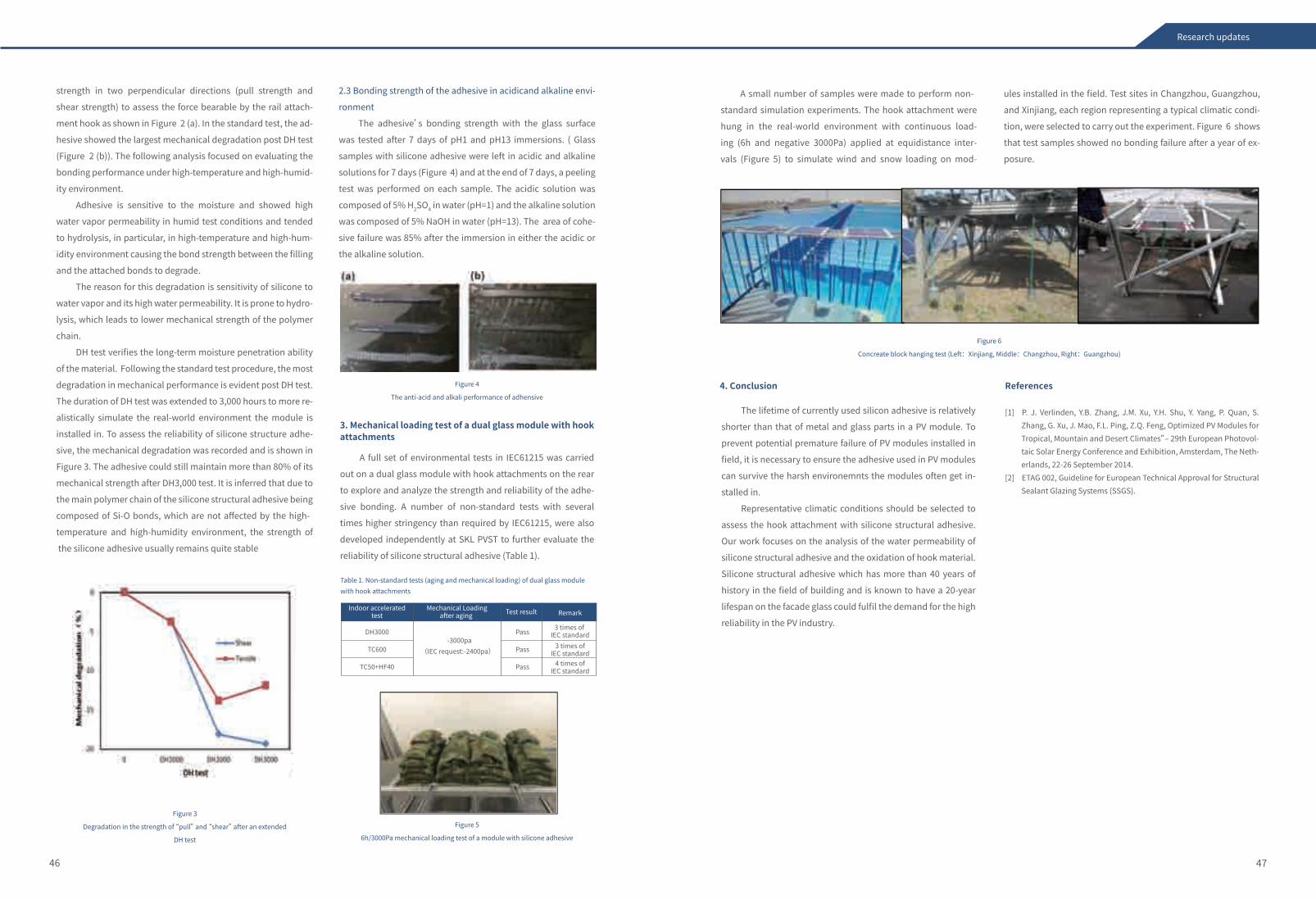
The lifetime of currently used silicon adhesive is relatively
shorter than that of metal and glass parts in a PV module. To
prevent potential premature failure of PV modules installed in
field, it is necessary to ensure the adhesive used in PV modules
can survive the harsh environemnts the modules often get in-
stalled in.
Representative climatic conditions should be selected to
assess the hook attachment with silicone structural adhesive.
Our work focuses on the analysis of the water permeability of
silicone structural adhesive and the oxidation of hook material.
Silicone structural adhesive which has more than 40 years of
history in the field of building and is known to have a 20-year
lifespan on the facade glass could fulfil the demand for the high
reliability in the PV industry.
4. Conclusion
A small number of samples were made to perform non-
standard simulation experiments. The hook attachment were
hung in the real-world environment with continuous load-
ing (6h and negative 3000Pa) applied at equidistance inter-
vals (Figure 5) to simulate wind and snow loading on mod-
ules installed in the field. Test sites in Changzhou, Guangzhou,
and Xinjiang, each region representing a typical climatic condi-
tion, were selected to carry out the experiment. Figure 6 shows
that test samples showed no bonding failure after a year of ex-
posure.
Figure 6
Concreate block hanging test (Left:Xinjiang, Middle:Changzhou, Right:Guangzhou)
References
[1] P. J. Verlinden, Y.B. Zhang, J.M. Xu, Y.H. Shu, Y. Yang, P. Quan, S. Zhang, G. Xu, J. Mao, F.L. Ping, Z.Q. Feng, Optimized PV Modules for Tropical, Mountain and Desert Climates”‒ 29th European Photovol-taic Solar Energy Conference and Exhibition, Amsterdam, The Neth-erlands, 22-26 September 2014.
[2] ETAG 002, Guideline for European Technical Approval for Structural Sealant Glazing Systems (SSGS).
A full set of environmental tests in IEC61215 was carried
out on a dual glass module with hook attachments on the rear
to explore and analyze the strength and reliability of the adhe-
sive bonding. A number of non-standard tests with several
times higher stringency than required by IEC61215, were also
developed independently at SKL PVST to further evaluate the
reliability of silicone structural adhesive (Table 1).
3. Mechanical loading test of a dual glass module with hook attachments
4746
Research updates
DH3000
TC600
TC50+HF40
-3000pa(IEC request:-2400pa)
Pass
Pass
Pass
3 times of IEC standard
3 times ofIEC standard
4 times ofIEC standard
Indoor acceleratedtest
Mechanical Loadingafter aging Test result Remark
Table 1. Non-standard tests (aging and mechanical loading) of dual glass module with hook attachments
Figure 3
Degradation in the strength of “pull” and “shear” after an extended
DH test
Figure 4
The anti-acid and alkali performance of adhensive
Figure 5
6h/3000Pa mechanical loading test of a module with silicone adhesive
(a)acidic (pH = 1) immersion (b)alkaline (pH=13) immersion
2.3 Bonding strength of the adhesive in acidicand alkaline envi-
ronment
The adhesive’s bonding strength with the glass surface
was tested after 7 days of pH1 and pH13 immersions. ( Glass
samples with silicone adhesive were left in acidic and alkaline
solutions for 7 days (Figure 4) and at the end of 7 days, a peeling
test was performed on each sample. The acidic solution was
composed of 5% H2SO4 in water (pH=1) and the alkaline solution
was composed of 5% NaOH in water (pH=13). The area of cohe-
sive failure was 85% after the immersion in either the acidic or
the alkaline solution.
strength in two perpendicular directions (pull strength and
shear strength) to assess the force bearable by the rail attach-
ment hook as shown in Figure 2 (a). In the standard test, the ad-
hesive showed the largest mechanical degradation post DH test
(Figure 2 (b)). The following analysis focused on evaluating the
bonding performance under high-temperature and high-humid-
ity environment.
Adhesive is sensitive to the moisture and showed high
water vapor permeability in humid test conditions and tended
to hydrolysis, in particular, in high-temperature and high-hum-
idity environment causing the bond strength between the filling
and the attached bonds to degrade.
The reason for this degradation is sensitivity of silicone to
water vapor and its high water permeability. It is prone to hydro-
lysis, which leads to lower mechanical strength of the polymer
chain.
DH test verifies the long-term moisture penetration ability
of the material. Following the standard test procedure, the most
degradation in mechanical performance is evident post DH test.
The duration of DH test was extended to 3,000 hours to more re-
alistically simulate the real-world environment the module is
installed in. To assess the reliability of silicone structure adhe-
sive, the mechanical degradation was recorded and is shown in
Figure 3. The adhesive could still maintain more than 80% of its
mechanical strength after DH3,000 test. It is inferred that due to
the main polymer chain of the silicone structural adhesive being
composed of Si-O bonds, which are not affected by the high-
temperature and high-humidity environment, the strength of
the silicone adhesive usually remains quite stable
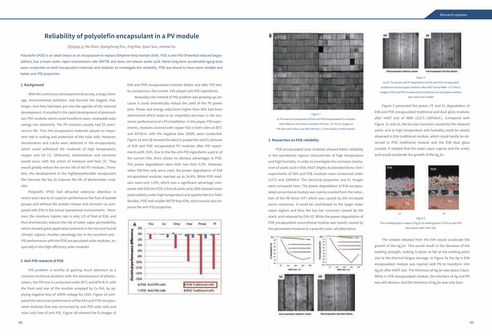
POE encapsulated solar modules showed better reliability
in the operational regions characteristic of high temperature
and high humidity. In order to investigate the corrosion mecha-
nism of acetic acid in EVA, HAST (Highly Accelerated Stress Test )
experiments of EVA and POE modules were conducted under
121℃ and 100%R.H. The electrical properties and EL images
were compared here. The power degradation of EVA encapsu-
lated conventional module was mainly resulted from the reduc-
tion of the fill factor (FF) which was caused by the increased
series resistance. it could be contributed to the larger water
vapor ingress and thus the bus bar corrosion caused by the
acetic acid released by EVA [4]. While the power degradation of
POE encapsulated conventional module was mainly caused by
the permeated moisture to cause the solar cell deteriation.
Figure 2 presented the power, FF and EL degradation of
EVA and POE encapsulated traditional and dual glass modules
after HAST test of 480h (121℃,100%R.H.). Compared with
Figure 2c and 2e, the bus bar corrosion caused by the released
acetic acid in high temperature and humidity could be clearly
observed in EVA traditional module, which could hardly be ob-
served in POE traditional module and the EVA dual glass
module. It implied that the water vapor ingress and the acetic
acid would accelerate the growth of the Ag3Sn.
The acetate released from the EVA would accelerate the
growth of the Ag3Sn. This would result in the decrease of the
welding strength, making it easier to fail at the welding point
due to the thermal fatigue damage. In Figure 3a the Ag in EVA
encapsulated module was reacted with Pb to transform into
Ag3Sn after HAST test. The thickness of Ag3Sn was about 13μm.
While in POE encapsulated module, the interface of Ag and Pb
was still obvious. And the thickness of Ag3Sn was only 5μm.
3. Researches on POE reliability
Figure 1
A) The electrical properties of EVA and POE encapsulated PV modules
with different cells before and after PID test;B) The EL images of
PID-free cells before and after PID test, a- EVA module, b-POE module.
Figure 2
(a),(b) The power and FF degradation of EVA and POE encapsulated
traditional and dual glass modules after HAST test of 480h. c~f) The EL
images of EVA and POE encapsulated traditional and dual glass modules
after HAST test of 480h
Figure 3
(The metallographic images of Ag3Sn at welding point of EVA (a) and POE
(b)modules after HAST test
(a) (b)
Polyolefin (POE) is an ideal choice as an encapsulant to replace Ethylene-Vinyl Acetate (EVA). POE is anti-PID (Potential Induced Degra-
dation), has a lower water vapor transmission rate (WVTR) and does not release acetic acid. Harsh long-term accelerated aging tests
were conducted on both encapsulant materials and modules to investigate the reliability. POE was found to have more reliable and
better anti-PID properties.
Reliability of polyolefin encapsulant in a PV moduleZhichao Ji, Hui Shen, Qiangzhong Zhu, Jing Mao, Quan Sun, Jianmei Xu
With the continuous development of society, energy short-
age, environmental pollution, had become the biggest chal-
lenges. And they had been put into the agenda of the national
development. It resulted in the rapid development of photovol-
taic (PV) modules which could transform clean, renewable solar
energy into electricity. The PV modules usually had 25 years’
service life. Thus the encapsulant materials played an impor-
tant role in sealing and protection of the solar cells. However,
discoloration and cracks were detected in the encapsulants,
which could withstand the multirole of high temperature,
oxygen and UV [1]. Otherwise, delamination and corrosion
would occur with the action of moisture and heat [2]. They
would greatly reduce the service life of the PV modules. There-
fore, the development of the highlyweatherable encapsulant
film became the key to improve the life of photovoltaic mod-
ules.
Polyolefin (POE) had attracted extensive attention in
recent years due to its superior performance like free of acetate
groups and without the acetate release and corrosion as com-
pared with EVA in the actual operational environments. More-
over, the moisture ingress rate is only 1/6 of that of EVA, and
thus dramatically reduces the risk of water vapor permeability,
which showed great application potential in the hot and humid
climatic regions. Another advantage lies in the excellent anti-
PID performance with the POE encapsulated solar modules, es-
specially in the high-efficiency solar modules
EVA and POE encapsulated modules before and after PID test.
by comparison, the current EVA adopts anti-PID ingredients.
Nowadays the interest of PID problem was growing up, be-
cause it could dramatically reduce the yield of the PV power
plan. Power and energy reductions higher than 30% had been
determined which leads to an important decrease in the eco-
nomic performance of a PV installation. In this paper, PID exper-
iments, modules covered with copper foil in both sides at 85℃
and 85%R.H. with the negative bias 1000V, were conducted.
Figure 1A and 1B showed the electric properties and EL pictures
of EVA and POE encapsulated PV modules after PID experi-
ments with 192h. Due to the the anti-PID ingredients used in of
the current EVA, there shows no obvious advantages in POE.
The power degradation were both less than 0.5%. However,
when PID-free cells were used, the power degradation of EVA
encapsulated modules reached up to 14.4%. While POE mod-
ules were only 1.6%, which was a significant advantage com-
pared with EVA the POE is free of acetic acid, AND showed lower
polarizability under high temperature and applied electric field.
Besides, POE had smaller WVTR than EVA, which would also im-
prove the anti-PID properties.
1. Background
PID problem is worthy of gaining much attention as a
common technical problem with the development of photov-
oltaics. the PID test is conducted under 85℃ and 85% R.H. with
the front and rear of the module wrapped by Cu foil, by ap-
plying negative bias of 1000V voltage for 192h. Figure 1A com-
pared the electrical performance of the EVA and POE encapsu-
lated modules that was connected by anti-PID solar cells and
solar cells free of anti-PID. Figure 1B showed the ELimages of
2. Anti-PID research of POE
4948
Research updates
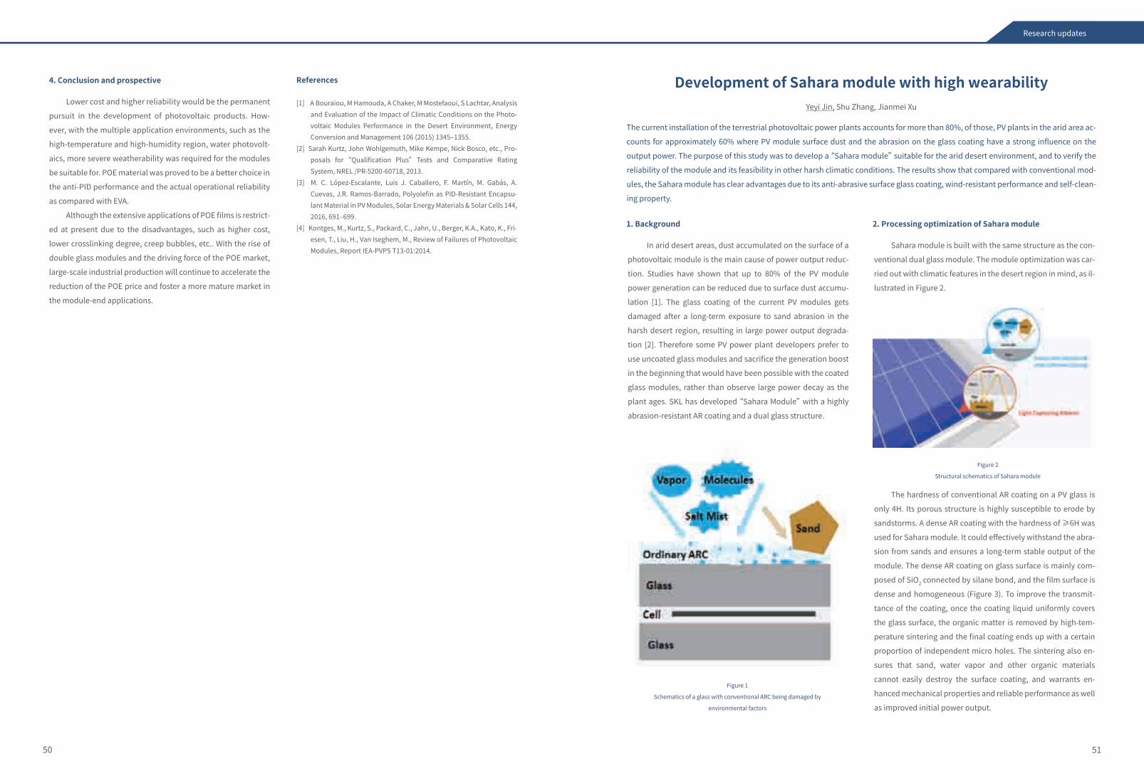
The current installation of the terrestrial photovoltaic power plants accounts for more than 80%, of those, PV plants in the arid area ac-
counts for approximately 60% where PV module surface dust and the abrasion on the glass coating have a strong influence on the
output power. The purpose of this study was to develop a “Sahara module” suitable for the arid desert environment, and to verify the
reliability of the module and its feasibility in other harsh climatic conditions. The results show that compared with conventional mod-
ules, the Sahara module has clear advantages due to its anti-abrasive surface glass coating, wind-resistant performance and self-clean-
ing property.
Development of Sahara module with high wearabilityYeyi Jin, Shu Zhang, Jianmei Xu
In arid desert areas, dust accumulated on the surface of a
photovoltaic module is the main cause of power output reduc-
tion. Studies have shown that up to 80% of the PV module
power generation can be reduced due to surface dust accumu-
lation [1]. The glass coating of the current PV modules gets
damaged after a long-term exposure to sand abrasion in the
harsh desert region, resulting in large power output degrada-
tion [2]. Therefore some PV power plant developers prefer to
use uncoated glass modules and sacrifice the generation boost
in the beginning that would have been possible with the coated
glass modules, rather than observe large power decay as the
plant ages. SKL has developed “Sahara Module” with a highly
abrasion-resistant AR coating and a dual glass structure.
1. Background
Sahara module is built with the same structure as the con-
ventional dual glass module. The module optimization was car-
ried out with climatic features in the desert region in mind, as il-
lustrated in Figure 2.
The hardness of conventional AR coating on a PV glass is
only 4H. Its porous structure is highly susceptible to erode by
sandstorms. A dense AR coating with the hardness of ≥6H was
used for Sahara module. It could effectively withstand the abra-
sion from sands and ensures a long-term stable output of the
module. The dense AR coating on glass surface is mainly com-
posed of SiO2 connected by silane bond, and the film surface is
dense and homogeneous (Figure 3). To improve the transmit-
tance of the coating, once the coating liquid uniformly covers
the glass surface, the organic matter is removed by high-tem-
perature sintering and the final coating ends up with a certain
proportion of independent micro holes. The sintering also en-
sures that sand, water vapor and other organic materials
cannot easily destroy the surface coating, and warrants en-
hanced mechanical properties and reliable performance as well
as improved initial power output.
2. Processing optimization of Sahara module
Figure 1
Schematics of a glass with conventional ARC being damaged by
environmental factors
Figure 2
Structural schematics of Sahara module
Lower cost and higher reliability would be the permanent
pursuit in the development of photovoltaic products. How-
ever, with the multiple application environments, such as the
high-temperature and high-humidity region, water photovolt-
aics, more severe weatherability was required for the modules
be suitable for. POE material was proved to be a better choice in
the anti-PID performance and the actual operational reliability
as compared with EVA.
Although the extensive applications of POE films is restrict-
ed at present due to the disadvantages, such as higher cost,
lower crosslinking degree, creep bubbles, etc.. With the rise of
double glass modules and the driving force of the POE market,
large-scale industrial production will continue to accelerate the
reduction of the POE price and foster a more mature market in
the module-end applications.
4. Conclusion and prospective
5150
Research updates
References
[1] A Bouraiou, M Hamouda, A Chaker, M Mostefaoui, S Lachtar, Analysis and Evaluation of the Impact of Climatic Conditions on the Photo-voltaic Modules Performance in the Desert Environment, Energy Conversion and Management 106 (2015) 1345‒1355.
[2] Sarah Kurtz, John Wohlgemuth, Mike Kempe, Nick Bosco, etc., Pro-posals for “Qualification Plus” Tests and Comparative Rating System, NREL /PR-5200-60718, 2013.
[3] M. C. López-Escalante, Luis J. Caballero, F. Martín, M. Gabás, A. Cuevas, J.R. Ramos-Barrado, Polyolefin as PID-Resistant Encapsu-lant Material in PV Modules, Solar Energy Materials & Solar Cells 144, 2016, 691‒699.
[4] Kontges, M., Kurtz, S., Packard, C., Jahn, U., Berger, K.A., Kato, K., Fri-esen, T., Liu, H., Van Iseghem, M., Review of Failures of Photovoltaic Modules, Report IEA-PVPS T13-01:2014.
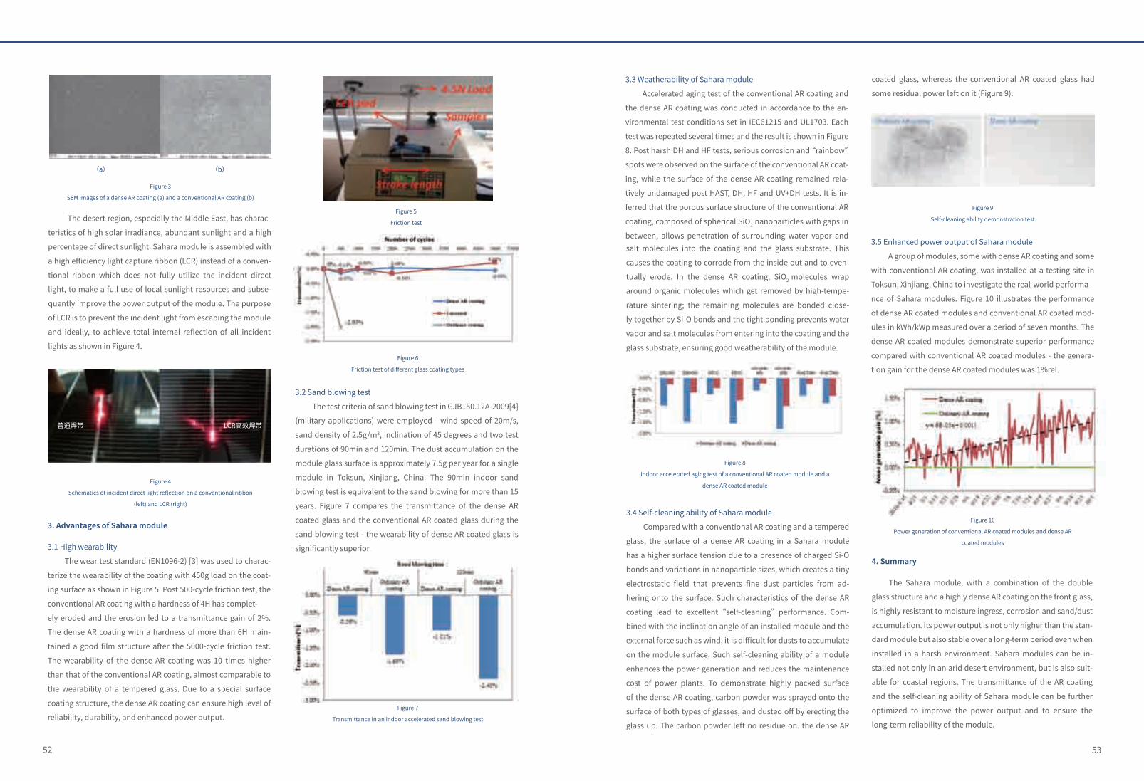
(a) (b)
The Sahara module, with a combination of the double
glass structure and a highly dense AR coating on the front glass,
is highly resistant to moisture ingress, corrosion and sand/dust
accumulation. Its power output is not only higher than the stan-
dard module but also stable over a long-term period even when
installed in a harsh environment. Sahara modules can be in-
stalled not only in an arid desert environment, but is also suit-
able for coastal regions. The transmittance of the AR coating
and the self-cleaning ability of Sahara module can be further
optimized to improve the power output and to ensure the
long-term reliability of the module.
4. Summary
5352
Figure 8
Indoor accelerated aging test of a conventional AR coated module and a
dense AR coated module
Figure 10
Power generation of conventional AR coated modules and dense AR
coated modules
Figure 9
Self-cleaning ability demonstration test
Figure 3
SEM images of a dense AR coating (a) and a conventional AR coating (b)
Figure 4
Schematics of incident direct light reflection on a conventional ribbon
(left) and LCR (right)
Figure 6
Friction test of different glass coating types
Figure 7
Transmittance in an indoor accelerated sand blowing test
Figure 5
Friction test
普通焊带 LCR高效焊带
3. Advantages of Sahara module
3.1 High wearability
The wear test standard (EN1096-2) [3] was used to charac-
terize the wearability of the coating with 450g load on the coat-
ing surface as shown in Figure 5. Post 500-cycle friction test, the
conventional AR coating with a hardness of 4H has complet-
ely eroded and the erosion led to a transmittance gain of 2%.
The dense AR coating with a hardness of more than 6H main-
tained a good film structure after the 5000-cycle friction test.
The wearability of the dense AR coating was 10 times higher
than that of the conventional AR coating, almost comparable to
the wearability of a tempered glass. Due to a special surface
coating structure, the dense AR coating can ensure high level of
reliability, durability, and enhanced power output.
3.2 Sand blowing test
The test criteria of sand blowing test in GJB150.12A-2009[4]
(military applications) were employed - wind speed of 20m/s,
sand density of 2.5g/m3, inclination of 45 degrees and two test
durations of 90min and 120min. The dust accumulation on the
module glass surface is approximately 7.5g per year for a single
module in Toksun, Xinjiang, China. The 90min indoor sand
blowing test is equivalent to the sand blowing for more than 15
years. Figure 7 compares the transmittance of the dense AR
coated glass and the conventional AR coated glass during the
sand blowing test - the wearability of dense AR coated glass is
significantly superior.
3.3 Weatherability of Sahara module
Accelerated aging test of the conventional AR coating and
the dense AR coating was conducted in accordance to the en-
vironmental test conditions set in IEC61215 and UL1703. Each
test was repeated several times and the result is shown in Figure
8. Post harsh DH and HF tests, serious corrosion and “rainbow”
spots were observed on the surface of the conventional AR coat-
ing, while the surface of the dense AR coating remained rela-
tively undamaged post HAST, DH, HF and UV+DH tests. It is in-
ferred that the porous surface structure of the conventional AR
coating, composed of spherical SiO2 nanoparticles with gaps in
between, allows penetration of surrounding water vapor and
3.4 Self-cleaning ability of Sahara module
Compared with a conventional AR coating and a tempered
glass, the surface of a dense AR coating in a Sahara module
has a higher surface tension due to a presence of charged Si-O
bonds and variations in nanoparticle sizes, which creates a tiny
electrostatic field that prevents fine dust particles from ad-
hering onto the surface. Such characteristics of the dense AR
coating lead to excellent “self-cleaning” performance. Com-
bined with the inclination angle of an installed module and the
external force such as wind, it is difficult for dusts to accumulate
on the module surface. Such self-cleaning ability of a module
enhances the power generation and reduces the maintenance
cost of power plants. To demonstrate highly packed surface
of the dense AR coating, carbon powder was sprayed onto the
surface of both types of glasses, and dusted off by erecting the
glass up. The carbon powder left no residue on. the dense AR
3.5 Enhanced power output of Sahara module
A group of modules, some with dense AR coating and some
with conventional AR coating, was installed at a testing site in
Toksun, Xinjiang, China to investigate the real-world performa-
nce of Sahara modules. Figure 10 illustrates the performance
of dense AR coated modules and conventional AR coated mod-
ules in kWh/kWp measured over a period of seven months. The
dense AR coated modules demonstrate superior performance
compared with conventional AR coated modules - the genera-
tion gain for the dense AR coated modules was 1%rel.
salt molecules into the coating and the glass substrate. This
causes the coating to corrode from the inside out and to even-
tually erode. In the dense AR coating, SiO2 molecules wrap
around organic molecules which get removed by high-tempe-
rature sintering; the remaining molecules are bonded close-
ly together by Si-O bonds and the tight bonding prevents water
vapor and salt molecules from entering into the coating and the
glass substrate, ensuring good weatherability of the module.
The desert region, especially the Middle East, has charac-
teristics of high solar irradiance, abundant sunlight and a high
percentage of direct sunlight. Sahara module is assembled with
a high efficiency light capture ribbon (LCR) instead of a conven-
tional ribbon which does not fully utilize the incident direct
light, to make a full use of local sunlight resources and subse-
quently improve the power output of the module. The purpose
of LCR is to prevent the incident light from escaping the module
and ideally, to achieve total internal reflection of all incident
lights as shown in Figure 4.
coated glass, whereas the conventional AR coated glass had
some residual power left on it (Figure 9).
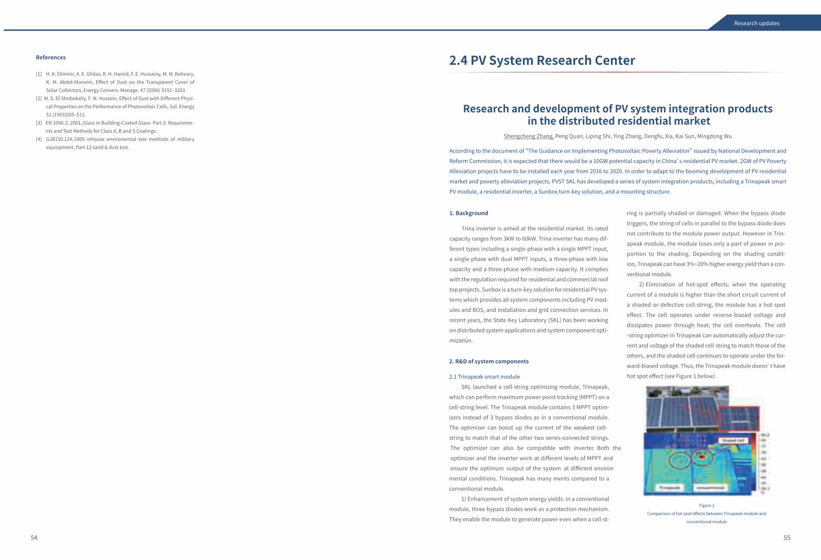
2. R&D of system components
2.1 Trinapeak smart module
SKL launched a cell-string optimizing module, Trinapeak,
which can perform maximum power point tracking (MPPT) on a
cell-string level. The Trinapeak module contains 3 MPPT optim-
izers instead of 3 bypass diodes as in a conventional module.
The optimizer can boost up the current of the weakest cell-
string to match that of the other two series-connected strings.
The optimizer can also be compatible with inverter. Both the
optimizer and the inverter work at different levels of MPPT and
ensure the optimum output of the system at different environ
mental conditions. Trinapeak has many merits compared to a
conventional module.
1) Enhancement of system energy yields: In a conventional
module, three bypass diodes work as a protection mechanism.
They enable the module to generate power even when a cell-st-
According to the document of “The Guidance on Implementing Photovoltaic Poverty Alleviation” issued by National Development and
Reform Commission, it is expected that there would be a 10GW potential capacity in China’s residential PV market. 2GW of PV Poverty
Alleviation projects have to be installed each year from 2016 to 2020. In order to adapt to the booming development of PV residential
market and poverty alleviation projects, PVST SKL has developed a series of system integration products, including a Trinapeak smart
PV module, a residential inverter, a Sunbox turn-key solution, and a mounting structure.
Research and development of PV system integration products in the distributed residential market
Shengcheng Zhang, Peng Quan, Liping Shi, Ying Zhang, Dengfu, Xia, Kai Sun, Mingdong Wu
2.4 PV System Research Center
The Sahara module, with a combination of the double
glass structure and a highly dense AR coating on the front glass,
is highly resistant to moisture ingress, corrosion and sand/dust
accumulation. Its power output is not only higher than the stan-
dard module but also stable over a long-term period even when
installed in a harsh environment. Sahara modules can be in-
stalled not only in an arid desert environment, but is also suit-
able for coastal regions. The transmittance of the AR coating
and the self-cleaning ability of Sahara module can be further
optimized to improve the power output and to ensure the
long-term reliability of the module.
Trina inverter is aimed at the residential market. Its rated
capacity ranges from 3kW to 60kW. Trina inverter has many dif-
ferent types including a single-phase with a single MPPT input,
a single-phase with dual MPPT inputs, a three-phase with low
capacity and a three-phase with medium capacity. It complies
with the regulation required for residential and commercial roof
top projects. Sunbox is a turn-key solution for residential PV sys-
tems which provides all system components including PV mod-
ules and BOS, and installation and grid connection services. In
recent years, the State Key Laboratory (SKL) has been working
on distributed system applications and system component opti-
mization.
ring is partially shaded or damaged. When the bypass diode
triggers, the string of cells in parallel to the bypass diode does
not contribute to the module power output. However in Trin-
apeak module, the module loses only a part of power in pro-
portion to the shading. Depending on the shading condit-
ion, Trinapeak can have 3%~20% higher energy yield than a con-
ventional module.
2) Elimination of hot-spot effects: when the operating
current of a module is higher than the short circuit current of
a shaded or defective cell-string, the module has a hot spot
effect. The cell operates under reverse-biased voltage and
dissipates power through heat; the cell overheats. The cell
-string optimizer in Trinapeak can automatically adjust the cur-
rent and voltage of the shaded cell-string to match those of the
others, and the shaded cell continues to operate under the for-
ward-biased voltage. Thus, the Trinapeak module doesn’t have
hot spot effect (see Figure 1 below).
1. Background
5554
Research updates
Figure 1
Comparison of hot spot effects between Trinapeak module and
conventional module
References
[1] H. K. Eliminir, A. E. Ghitas, R. H. Hamid, F. E. Hussainy, M. M. Beheary, K. M. Abdel-Moneim, Effect of Dust on the Transparent Cover of Solar Collectors, Energy Convers. Manage. 47 (2006) 3192‒3203.
[2] M. S. El-Shobokshy, F. M. Hussein, Effect of Dust with Different Physi-cal Properties on the Performance of Photovoltaic Cells, Sol. Energy 51 (1993)505‒511.
[3] EN 1096-2:2001,Glass in Building-Coated Glass- Part 2: Requireme- nts and Test Methods for Class A, B and S Coatings.[4] GJB150.12A-2009 inhouse environemtal test methods of military
equiopment, Part 12:sand & dust test.
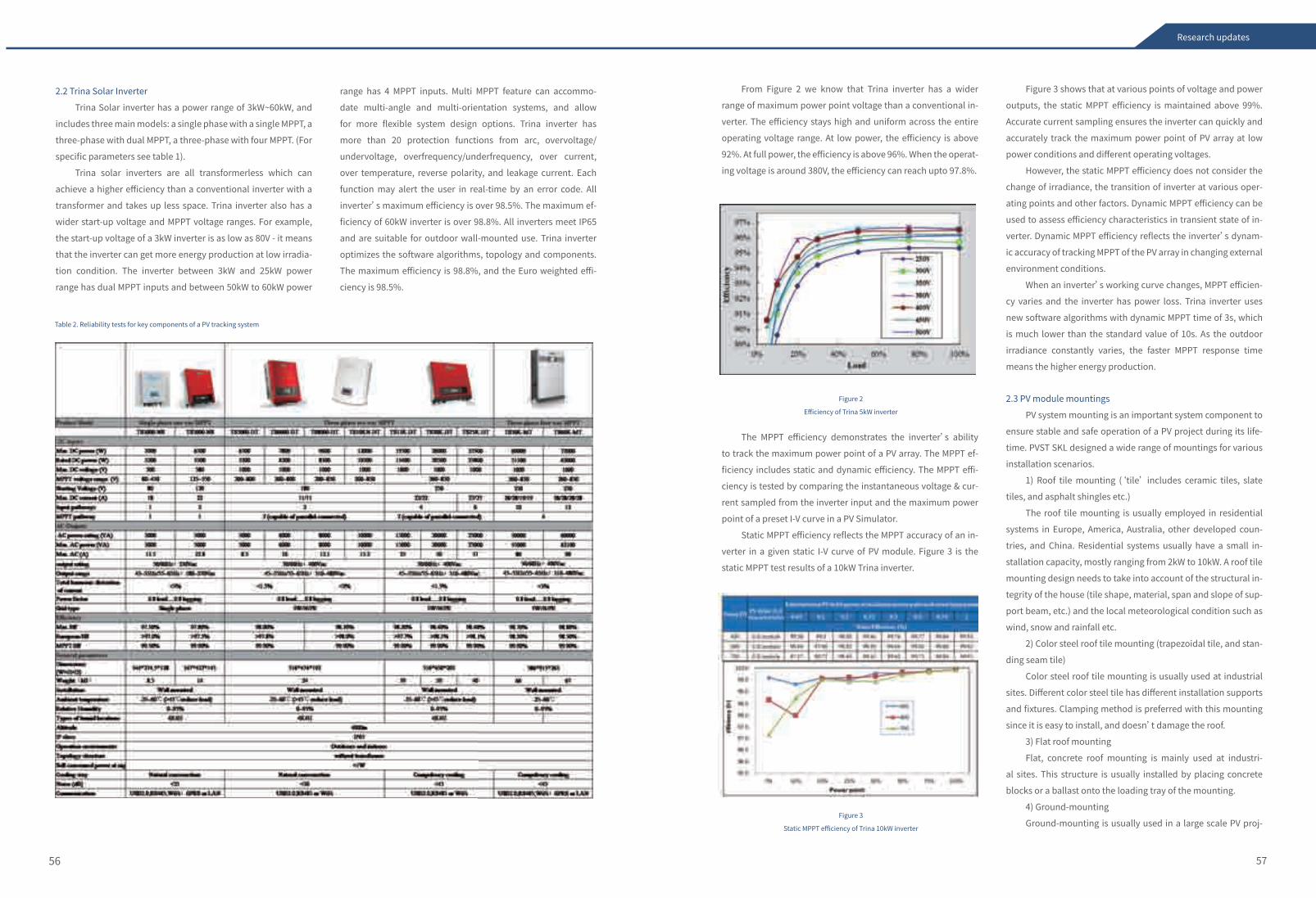
2.2 Trina Solar Inverter
Trina Solar inverter has a power range of 3kW~60kW, and
includes three main models: a single phase with a single MPPT, a
three-phase with dual MPPT, a three-phase with four MPPT. (For
specific parameters see table 1).
Trina solar inverters are all transformerless which can
achieve a higher efficiency than a conventional inverter with a
transformer and takes up less space. Trina inverter also has a
wider start-up voltage and MPPT voltage ranges. For example,
the start-up voltage of a 3kW inverter is as low as 80V - it means
that the inverter can get more energy production at low irradia-
tion condition. The inverter between 3kW and 25kW power
range has dual MPPT inputs and between 50kW to 60kW power
range has 4 MPPT inputs. Multi MPPT feature can accommo-
date multi-angle and multi-orientation systems, and allow
for more flexible system design options. Trina inverter has
more than 20 protection functions from arc, overvoltage/
undervoltage, overfrequency/underfrequency, over current,
over temperature, reverse polarity, and leakage current. Each
function may alert the user in real-time by an error code. All
inverter’s maximum efficiency is over 98.5%. The maximum ef-
ficiency of 60kW inverter is over 98.8%. All inverters meet IP65
and are suitable for outdoor wall-mounted use. Trina inverter
optimizes the software algorithms, topology and components.
The maximum efficiency is 98.8%, and the Euro weighted effi-
ciency is 98.5%.
From Figure 2 we know that Trina inverter has a wider
range of maximum power point voltage than a conventional in-
verter. The efficiency stays high and uniform across the entire
operating voltage range. At low power, the efficiency is above
92%. At full power, the efficiency is above 96%. When the operat-
ing voltage is around 380V, the efficiency can reach upto 97.8%.
Figure 3 shows that at various points of voltage and power
outputs, the static MPPT efficiency is maintained above 99%.
Accurate current sampling ensures the inverter can quickly and
accurately track the maximum power point of PV array at low
power conditions and different operating voltages.
However, the static MPPT efficiency does not consider the
change of irradiance, the transition of inverter at various oper-
ating points and other factors. Dynamic MPPT efficiency can be
used to assess efficiency characteristics in transient state of in-
verter. Dynamic MPPT efficiency reflects the inverter’s dynam-
ic accuracy of tracking MPPT of the PV array in changing external
environment conditions.
When an inverter’s working curve changes, MPPT efficien-
cy varies and the inverter has power loss. Trina inverter uses
new software algorithms with dynamic MPPT time of 3s, which
is much lower than the standard value of 10s. As the outdoor
irradiance constantly varies, the faster MPPT response time
means the higher energy production.
The MPPT efficiency demonstrates the inverter’s ability
to track the maximum power point of a PV array. The MPPT ef-
ficiency includes static and dynamic efficiency. The MPPT effi-
ciency is tested by comparing the instantaneous voltage & cur-
rent sampled from the inverter input and the maximum power
point of a preset I-V curve in a PV Simulator.
Static MPPT efficiency reflects the MPPT accuracy of an in-
verter in a given static I-V curve of PV module. Figure 3 is the
static MPPT test results of a 10kW Trina inverter.
5756
Research updates
Figure 2
Efficiency of Trina 5kW inverter
Figure 3
Static MPPT efficiency of Trina 10kW inverter
2.3 PV module mountings
PV system mounting is an important system component to
ensure stable and safe operation of a PV project during its life-
time. PVST SKL designed a wide range of mountings for various
installation scenarios.
1) Roof tile mounting (‘tile’ includes ceramic tiles, slate
tiles, and asphalt shingles etc.)
The roof tile mounting is usually employed in residential
systems in Europe, America, Australia, other developed coun-
tries, and China. Residential systems usually have a small in-
stallation capacity, mostly ranging from 2kW to 10kW. A roof tile
mounting design needs to take into account of the structural in-
tegrity of the house (tile shape, material, span and slope of sup-
port beam, etc.) and the local meteorological condition such as
wind, snow and rainfall etc.
2) Color steel roof tile mounting (trapezoidal tile, and stan-
ding seam tile)
Color steel roof tile mounting is usually used at industrial
sites. Different color steel tile has different installation supports
and fixtures. Clamping method is preferred with this mounting
since it is easy to install, and doesn’t damage the roof.
3) Flat roof mounting
Flat, concrete roof mounting is mainly used at industri-
al sites. This structure is usually installed by placing concrete
blocks or a ballast onto the loading tray of the mounting.
4) Ground-mounting
Ground-mounting is usually used in a large scale PV proj-
Table 2. Reliability tests for key components of a PV tracking system
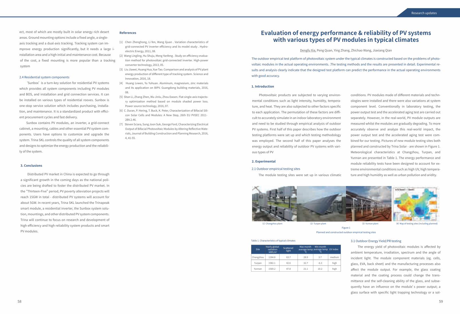
2. Experimental
conditions. PV modules made of different materials and techn-
ologies were installed and there were also variations at system
component level. Conventionally in laboratory testing, the
power output test and the accelerated aging test are carried out
separately. However, in the real-world, PV module outputs are
measured whilst the modules are gradually degrading. To more
accurately observe and analyze this real-world impact, the
power output test and the accelerated aging test were com-
bined for our testing. Pictures of new module testing sites both
planned and constructed by Trina Solar - are shown in Figure 1.
Meteorological characteristics at Changzhou, Turpan, and
Yunnan are presented in Table 1. The energy performance and
module reliability tests have been designed to account for ex-
treme environmental conditions such as high UV, high tempera-
ture and high humidity as well as urban pollution and aridity.
3. Results and Discussion
3.1 Outdoor Energy Yield/PR testing
The energy yield of photovoltaic modules is affected by
ambient temperature, irradiation, spectrum and the angle of
incident light. The module component materials (eg. cells,
glass, EVA, back sheet) and the manufacturing processes also
affect the module output. For example, the glass coating
material and the coating process could change the trans-
mittance and the self-cleaning ability of the glass, and subse-
quently have an influence on the module’s power output; a
glass surface with specific light trapping technology or a sol-
The outdoor empirical test platform of photovoltaic system under the typical climates is constructed based on the problems of photo-
voltaic modules in the actual operating environments. .The testing methods and the results are presented in detail. Experimental re-
sults and analysis clearly indicate that the designed test platform can predict the performance in the actual operating environments
with good accuracy.
Evaluation of energy performance & reliability of PV systemswith various types of PV modules in typical climates
Dengfu Xia, Peng Quan, Ying Zhang, Zhichao Wang, Jiaxiang Qian
Photovoltaic products are subjected to varying environ-
mental conditions such as light intensity, humidity, tempera-
ture, and heat. They are also subjected to other factors specific
to each application. The permutation of these factors are diffi-
cult to accurately simulate in an indoor laboratory environment
and need to be studied through empirical analysis of outdoor
PV systems. First half of this paper describes how the outdoor
testing platforms were set up and which testing methodology
was employed. The second half of this paper analyses the
energy output and reliability of outdoor PV systems with vari-
ous types of PV
1. Introduction
Distributed PV market in China is expected to go through
a significant growth in the coming days as the national poli-
cies are being drafted to foster the distributed PV market. In
the “Thirteen-Five” period, PV poverty alleviation projects will
reach 15GW in total - distributed PV systems will account for
about 5GW. In recent years, Trina SKL launched the Trinapeak
smart module, a residential inverter, the Sunbox system solu-
tion, mountings, and other distributed PV system components.
Trina will continue to focus on research and development of
high efficiency and high reliability system products and smart
PV modules.
3. Conclusions
59 58
Research updates
Figure 1
Planned and constructed outdoor empirical testing sites
ect, most of which are mostly built in solar energy rich desert
areas. Ground mounting options include a fixed angle, a single-
axis tracking and a dual-axis tracking. Tracking system can im-
mprove energy production significantly, but it needs a large i-
nstallation area and a high initial and maintenance cost. Because
of the cost, a fixed mounting is more popular than a tracking
system
2.4 Residential system components
‘Sunbox’ is a turn-key solution for residential PV systems
which provides all system components including PV modules
and BOS, and installation and grid connection services. It can
be installed on various types of residential rooves. Sunbox is
one-stop service solution which includes purchasing, installa-
tion, and maintenance. It is a standardized product with effici-
ent procurement cycles and fast delivery.
Sunbox contains PV modules, an inverter, a grid-connect
cabinet, a mounting, cables and other essential PV system com-
ponents. Users have options to customize and upgrade the
system. Trina SKL controls the quality of all system components
and designs to optimize the energy production and the reliabili-
ty of the system.
References
[1] Chen Zhenghong, Li fen, Wang lijuan . Variation characteristics of grid-connected PV inverter efficiency and its model study . Hydro-electric Energy, 2011, 08.
[2] Wang Lingling, Hu Shuju, Meng Yanfeng . Study on efficiency evalua-tion method for photovoltaic grid-connected inverter. High-power converter technology, 2013, 05.
[3] Liu Jiawei, Huang Hua, Xue Tao. Comparison and analysis of PV plant energy production of different type of tracking system. Science and Innovation, 2016, 18.
[4] Huang Lvwen, Yu Yuhuan. Aluminum, magnesium, zinc materials and its application on BIPV. Guangdong building materials, 2016, 08.
[5] Shan Li, Zhang Zhen, Wu Jinlu, Zhou Daoen. Flat single-axis trajecto-ry optimization method based on module shaded power loss. Power source technology, 2016, 07.
[6] C. Duran, P. Hering, T. Buck, K. Peter, Characterization of Bifacial Sili-con Solar Cells and Modules: A New Step, 26th EU PVSEC 2011-2BV.2.46.
[7] Steven Sciara, Sung Joon Suk, George Ford, Characterizing Electrical Output of Bifacial Photovoltaic Modules by Altering Reflective Mate-rials, Journal of Building Construction and Planning Research, 2016, 4, 41-55.
(3) Yunnan plant (4) Map of testing sites (including planned)(1) Changzhou plant (2) Turpan plant
Table 1. Characteristics of typical climates
SiteYearly global
radiation kWh/m2
Scattered light
Min month average temp
℃UV index
Max month average temp
℃
Changzhou
Turpan
Yunnan
1264.8
1582.1
1569.2
63.7
42.6
47.8
28.9
32.7
21.1
3.7
-6.3
10.2
medium
high
high
2.1 Outdoor empirical testing sites
The module testing sites were set up in various climatic
3.2 Measurement of Incidence Angle Modifier (IAM)
IAM measurements were carried out to analyze the effects
of different incident angles on the performance of PV modules.
Figure 4 shows the adjusted IAM result of four modules which
were tested at Trina Solar Changzhou outdoor testing site. The
IAM value is greatly affected by outdoor weather conditions and
errors in the results were large. Therefore, multiple modules
should be selected and tested at the same time under ideal con-
ditions (high irradiation, high direct irradiation ratio, no wind,
stable weather).
3.3 Reliability testing of module component materials and mod-
ules
The long-term reliability tests included “hot-spot” test, PID
test and LID test. The hot-spot testing result infers that a smart
module is able to dissipate the heat better than a conventional
module (Figure 5). When a hot-spot incurs in a PV system, the
current in the shaded cell does not clip the entire string current
as the current in the shaded smart module is increased to match
the current in the string. This prevents the bypass diode in the
string being activated and the series cell voltage continues to
contribute to the overall module power output, effectively elim-
inating the hot-spot phenomenon.
der strip with inbuilt reflective microstructure could increase
the amount of light that is absorbed by cells and subsequently
increase the energy yield of a module.
A long-term outdoor energy yield testing was performed on
five types of modules. All the modules were made up of the
same materials and processes but had different types of glass ‒
some modules had ARC, while some did not have ARC. Pre-con-
ditioning and the subsequent power measurements were con-
ducted in an indoor laboratory on two to three sample modules
which were taken from each module type. Based on the data
from Trina Solar Changzhou outdoor module testing site taken
from 6th June, 2015 to 28th July, 2015, (shown in Figure 2) all
modules with ARC performed better than modules without ARC.
The maximum yield was approximately 2%.
Figure 3(2) shows the energy yield of the sample modules
with different manufacturing processes at Trina Solar Chang-
zhou outdoor testing site between 16th July, 2014 and 1st Sep-
tember, 2014. The outdoor sample module output is similar
to that of indoor power output under low irradiation which is
similar to the irradiation condition in Changzhou. It can be in-
ferred that, for low irradiation condition, indoor laboratory
testing can be a good estimate for modules’ real-world perfo-
rmance. This is good because, in the case of high performance
modules, the module performance under low irradiation also
matters, in addition to the module performance at STC.
6160
Research updates
Figure 2
Energy performance of modules in an outdoor testing site
Figure 3
Indoor and outdoor power performance of modules manufactured with
different processes Figure 4
Photovoltaic modules outdoor IAM test
Figure 5
Outdoor hot-spot test comparison between conventional and smart
modules
(1) Comparison of modules with different ARC
(1) Indoor power output at various irradiation level
(1) IAM tracking system
(2) Outdoor energy output
(2) IAM comparison test data
(2) The outdoor module testing site at Changzhou
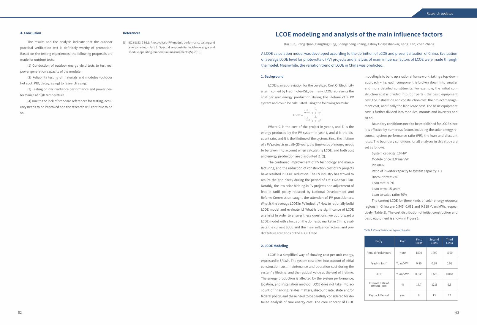
The results and the analysis indicate that the outdoor
practical verification test is definitely worthy of promotion.
Based on the testing experiences, the following proposals are
made for outdoor tests:
(1) Conduction of outdoor energy yield tests to test real
power generation capacity of the module.
(2) Reliability testing of materials and modules (outdoor
hot spot, PID, decay, aging) to research aging.
(3) Testing of low irradiance performance and power per-
formance at high temperature.
(4) Due to the lack of standard references for testing, accu-
racy needs to be improved and the research will continue to do
so.
4. Conclusion
LCOE is an abbreviation for the Levelized Cost Of Electricity
a term coined by Fraunhofer-ISE, Germany. LCOE represents the
cost per unit energy production during the lifetime of a PV
system and could be calculated using the following formula:
Where Ct is the cost of the project in year t, and Et is the
energy produced by the PV system in year t, and d is the dis-
count rate, and N is the lifetime of the system. Since the lifetime
of a PV project is usually 25 years, the time value of money needs
to be taken into account when calculating LCOE, and both cost
and energy production are discounted [1, 2].
The continued improvement of PV technology and manu-
facturing, and the reduction of construction cost of PV projects
have resulted in LCOE reduction. The PV industry has strived to
realize the grid parity during the period of 13th Five-Year Plan.
Notably, the low price bidding in PV projects and adjustment of
feed-in tariff policy released by National Development and
Reform Commission caught the attention of PV practitioners.
What is the average LCOE in PV industry? How to rationally build
LCOE model and evaluate it? What is the significance of LCOE
analysis? In order to answer these questions, we put forward a
LCOE model with a focus on the domestic market in China, eval-
uate the current LCOE and the main influence factors, and pre-
dict future scenarios of the LCOE trend.
1. Background
LCOE is a simplified way of showing cost per unit energy,
expressed in $/kWh. The system cost takes into account of initial
construction cost, maintenance and operation cost during the
system’s lifetime, and the residual value at the end of lifetime.
The energy production is affected by the system performance,
location, and installation method. LCOE does not take into ac-
count of financing relates matters, discount rate, state and/or
federal policy, and these need to be carefully considered for de-
tailed analysis of true energy cost. The core concept of LCOE
2. LCOE Modeling
modeling is to build up a rational frame work, taking a top-down
approach ‒ i.e. each component is broken down into smaller
and more detailed constituents. For example, the initial con-
struction cost is divided into four parts - the basic equipment
cost, the installation and construction cost, the project manage-
ment cost, and finally the land lease cost. The basic equipment
cost is further divided into modules, mounts and inverters and
so on.
Boundary conditions need to be established for LCOE since
it is affected by numerous factors including the solar energy re-
source, system performance ratio (PR), the loan and discount
rates. The boundary conditions for all analyses in this study are
set as follows.
System capacity: 10 MW
Module price: 3.0 Yuan/W
PR: 80%
Ratio of inverter capacity to system capacity: 1.1
Discount rate: 7%
Loan rate: 4.9%
Loan term: 15 years
Loan to value ratio: 70%
The current LCOE for three kinds of solar energy resource
regions in China are 0.545, 0.681 and 0.818 Yuan/kWh, respec-
tively (Table 1). The cost distribution of initial construction and
basic equipment is shown in Figure 1.
6362
LCOE modeling and analysis of the main influence factorsKai Sun, Peng Quan, Bangting Ding, Shengcheng Zhang, Ashray Udayashankar, Kang Jian, Zhen Zhang
A LCOE calculation model was developed according to the definition of LCOE and present situation of China. Evaluation of average LCOE level for photovoltaic (PV) projects and analysis of main influence factors of LCOE were made through the model. Meanwhile, the variation trend of LCOE in China was predicted.
Research updates
References
[1] IEC 61853-2 Ed.1: Photovoltaic (PV) module performance testing and energy rating - Part 2: Spectral responsivity, incidence angle and module operating temperature measurements [S]. 2016.
Table 1. Characteristics of typical climates
Annual Peak Hours
Feed-in Tariff
LCOE
Internal Rate ofReturn (IRR)
Payback Period
hour
Yuan/kWh
Yuan/kWh
%
year
1500
0.80
0.545
17.7
8
1200
0.88
0.681
12.5
13
1000
0.98
0.818
9.5
17
Entry Unit FirstClass
SecondClass
ThirdClass
=LCOE∑t
tt
tt
N C
E∑tN
0
0
(1 d)
(1 d)
+
+
=
=
1 Percentage stated below the smart module type label on the x-axis represents the energy gain relative to the conventional module
6564
Various factors affect the LCOE of a PV project. In this sec-
tion, four main factors are discussed.
3. Analysis of Main Influencing Factors
As the PV component technologies and manufacturing
technology advance, the cost of PV projects will decrease and
the subsequent LCOE will also continue to fall during the period
of 13th Five-Year Plan [3]. However, the scarcity of suitable land,
increasing labor cost and limited room for equipment price drop
are expected to resist significant reduction in LCOE in future.
Table 2 presents future scenarios of LCOE for the coming four
years.
4. Variation Trends of LCOE
We have successfully developed a LCOE calculation model
according to the research of PV industry in China. The estima-
tion of current LCOE level, analysis of main influence factors,
and prediction of variation trends were made. It is feasible to re-
alize grid parity in 2020 based on the current situation and de-
velopment of PV industry.
5. Conclusion
Research updates
Table 2. Variation trends of LCOE during the period of 13th Five-Year Plan
Figure 1
Cost distribution of initial construction and basic equipment of PV
projects
3.1 System Construction Cost
The impact system construction cost has on LCOE is ana-
lyzed while the total energy production remains constant. The
current construction cost of a PV project is less than 7 Yuan/W.
Since the module cost is the largest component of the initial
construction cost, approximately 40% to be exact (54.7% x
73.18% = 40%), the module price has been selected as a repre-
sentative construction cost. The test criteria are the same as the
above mentioned with the “second class” 1200 peak-hour solar
irradiation. Result of impact an increasing module cost has on
LCOE is shown in Figure 2 - when the module price is reduced by
0.1 Yuan/W, LCOE is reduced by 0.01 Yuan/kWh, which means
the other cost variations in construction cost part have the simi-
lar effects on LCOE, such as mounts, inverters, installation.
3.2 Solar Irradiation and PR
Solar irradiation and system PR have significant impacts on
LCOE. Three regions in China with different types of solar irradi-
ance have been selected for this study. Each region has been
classified according to the number of peak hours in a year -
more than 1400 hours has been classified first class while less
than 1200 hours has been classified the third class; between
1200 and 1400 peak-hour region has been classified the second
class.
Figure 3 shows the correlation among LCOE, peak hours
and PR. LCOE decreases with an increase of peak hours - as the
peak-hours increase from 1000 to 1800 hours, LCOE is reduced
by 44%. However, LCOE is inversely correlated to PR. For exam-
ple, LCOE is reduced by 17% when PR is increased from 75% to
90%. Though the first class region has an advantage of high
peak hours, we still have to objectively notice the existing phe-
nomenon of limited energy production.
3.3 Discount Rate and Loan Rate
PV projects belong to commercial investment. Tax, loan
and related capital financial are usually included in PV projects
as a result of high cost and long operating period. Therefore,
representative discount rate and loan rate were selected as an
example to study the effects of financing on LCOE (Figure 4) with
1200 peak-hours. LCOE is increased by 4% as discount rate is in-
creased by 1%. LCOE is increased by 3% as loan rate is increased
by 1%. We have to fully evaluate the economic development sit-
uation on the investment side.
3.4 Innovative Technology Development
Despite the initial capital injection for new products and
technologies development, the benefits of increased energy
generation reduce LCOE. As the technology matures and the
economies of scale reduce the cost, LCOE is further reduced. For
example, introduction of smart modules and tracking systems
have increased the cost, however LCOE was reduced because of
significant increase in energy production (Figure 5). The ongo-
ing operation and maintenance cost with smart modules is rela-
tively the same, if not lower, compared to the conventional
modules while the energy production is significantly higher
during the lifetime of the system; subsequently, LCOE is re-
duced. Not all currently available smart modules result in re-
duced LCOE if the additional energy production does not offset
the increase in cost ‒ for example, a bifacial module in Figure 5.
The analysis was carried out with the assumptions set
above and the peak-hour of 1200 hours (second class).
Figure 2
Impact of a module price on LCOE
Figure 3
Impact of solar irradiation and PR on LCOE
Figure 4
The influence of discount rate and loan rate on LCOE
Figure 5
Impact of innovative technology on LCOE1
2016
2017
2018
2019
2020
Yuan/kWh
0.545
0.518
0.492
0.467
0.444
0.681
0.647
0.615
0.584
0.555
0.818
0.777
0.738
0.701
0.666
Year Unit FirstClass
SecondClass
ThirdClass
References
[1] Chen Rongrong, Sun Yunlin, Chen Siming, Shen Hui. LCOE analysis of grid-connected photovoltaic power generation project. Renew-able Energy Resources [J], 2015, 5(133): 731-735.
[2] Wang Sicheng. High profit comes from technology innovation and good quality bases on fine design. Solar Energy [J], 2015, 6, 6-11.
[3] Zang Ningning. Analysis of cost of PV projects during the period of 13th Five-Year Plan. China Power Enterprise Management [J], 2016, 5, 50-53.
2) 2 high-precision and high-speed 6-axis robot arms are
used alternatively as per the computational anaylasis. This
scheme not only reduces the wafer breakage rate compared
with the manual handlilng but also increases the speed of
wafers being put into the box. and . The margin of error on the
positioning of a wafer into a box is ≤0.2mm. The repetition and
the positioning precision of the robot arm are controlled within
0.01mm and 0.05mm respectively to comply with the higher
throughput requirement of the cleaning machine.
3) A sucking device is employed to load the wafer. This
method has been selected in order to reduce the abrasion and
the contact contamination from the roller and the wafers in
contact. A contactless sucking device based on Bernoulli's Prin-
ciple is employed; the condensed air is exhausted through the
gaps between the wafer and the sucker. The sucker works even
on a rough wafer surface which a vacuum sucker is incapable of
completing. This sucking device has three advantages: a) con-
tactless suction elimminates waer breakage and contamina-
tion; b) large contact area and a homogenously applied force
ensure a low breakage rate; c) a long service life.
4) A vision system is required for high-speed positioning
and in-line detection of the wafer breakage. The positioning
precision needs to be within 0.02mm to accommodate the exis-
iting loading box and wafers, as well as the deformed box from
long-term usage. Two industrial high-speed smart camera with
5M resolution are used as a part of the vision system. the physi-
cal camera presents the single-resolution size of 0.15mm. The
imaging accuracy can reach up to 0.0218mm (0.175mm/8=
0.0218mm) level if followed by sub-pixel imaging, and image
-detection & positioning algorithm.
The EL defect-detection system can monitor and detect
defects in cells using the EL imaging technique. Various types of
defects can be accurately detected and sorted using this equip-
ment - material defects such as dislocation, abnormal doping,
and stacking fault; diffusion defects such as sheet resistance in-
homogeneity; screen printing defects such as broken lines;
firing defects such as the beltprint, and the contamination
during the processing. The main purpose of the integration is to
increase the cell yield, to enhance the sorting and to reduce the
material consumption and the cost.
Prior to the automatic detection, workers manually detect-
ed and classified cell and module defects using the EL images.
As the industry developed and grew, increasing quantity of cells
and modules needed to be quality controlled and disadvantag-
es of manual handling such as the eye fatigue and the variance
in classification among operators became increasingly pro-
nounced.
The automatic EL defect-detection technique splits and
extracts EL images followed by the defect analysis and detec-
tion. The automated analysis of a cell was cross-checked
against the output of the cell. The imaging technique includes
EL image capturing, antibarreling, the perspective transforma-
tion, gray scale correction and the segmentation of the cap-
tured EL image. This technique is capable of accurately detect-
ing fragments, cracks and broken lines as shown in Figure 4.
The key to the automatized defect detection lies in the de-
velopment of the software algorithm, in which an advanced al-
gorithm and the intelligent-learning neural network play a piv-
otal role in the accuracy of the detection. The accuracy also de-
pends on the input image quality - pixel, resolution, grayscale,
noise, and stray light. The key algorithm code for the edge is
shown below:
3. Contactless loading machineFigure 2
Schematic of an automatic loading in the chained cleaning machine
Figure 3
Schematics of the sucking device based on the Bernoulli's Principle
1 Percentage stated below the smart module type label on the x-axis represents the energy gain relative to the conventional module
66 67
PV equipment research center researches and developes new and existing manufacturing equipment domestically as the PV technolo-
gy advances and the industry grows at an accelerated rate, requiring reliable and high throughput equipment. This paper focuses on
the development of multi-functional laser doping equipment, an automatic contactless loading machine, an EL defect-detection vision
system and a multi-busbar stringer.
R&D of c-Si PV manufacturing equipment and its progressZhiqiang Ding, Chunyan Zhang, Zemin Yang, Liusheng Zhu, Haining Li, Lie Liu
2.5 Equipment Reseach Center
The rapid development of PV industry and the continuous
advancement of processing technologies are requiring the PV
manufacturing equipment to accommodate newly developed
processes, higher throughput and optimized performance. The
main purpose is to provide a favorable realization schema for
the laboratory experiments and the pilot production.
1. Background
To decrease the abrasion of cells on the convey belt, an au-
tomatic contactless wafer loading machine with a robotic arm
to reduce the contact contamination. The flexible top robotic
arm and a 6-axis wafer-sucking robot were equipped with an
absolute encoder to record the operation and the location. The
controller and the safety control module with high-speed CPU
could ensure the operational accuracy and stability and the
safety of the operator.
The automation mainly incorporates the following four
1) Roller contactless loading schema is utilized to reduce
the contact contamination between the wafer and the rollers.
Currently, the chained cleaning machine is connected to the
rolling conveyer made out of special materials. The wafer outlet
is equipped with two visiual positioning and computation sys-
tems to acquire an accurate location of a wafer. Figure 2 illus-
trates a schematic of an automatic loading, in the chained
cleaning machine.
3. Contactless loading machine
The newly developed laser doping technology has many
advantages over the conventional doping technology. It can ac-
curately control the heat input in the local region, form doped
areas directly which could be operated at ambient temperature
to reduce the thermal effect, and the processing is fast and
simply, and more suitable for thin silicon substrates. The tech-
nology would be useful for the rear local doping, and the abla-
tion of the dielectric passivation layer on the rear.
The core component of the laser doping equipment is the
laser. The energy density of the laser is related to the output
power and the diameter of the laser facula. The number of laser
pulses is related to the scanning speed of the scanning head.
Since the laser doping machine would be used to dope the sili-
con wafer, key laser parameters are adjusted for two main dop-
ants, phosphorous and boron, and the purpose of the experi-
ment: the maximum output power of 80W, the diameter of the
output facula in the range of 15μm~50μm by adjusting the laser
bean expander, the maximum repetition frequency of 1MHz,
and the maximum scanning head speed of 24m/s to reduce the
doping time. Figure 1 shows an average resultant sheet resis-
tance of the boron-doped substrate to be 30Ohm/sq.
2. Laser doping equipment Figure 1
Boron doped image: the average sheet resistance of 30 Ω/sq (left);
morphology of the boron doping (right)
Research updates
5. Automatic multi-busbar stringer
The rapid development of China’s PV industry necessi-
tates the technology innovation and the cost reduction to con-
tinue its exponential growth. In turn, the technology innovation
requires the development of appropriate PV equipment to ac-
commodate the changing technologies in the manufacturing
line.
Under the directives of the Chinese government with pro-
grams such as “internet +” and “made in China 2025 Plan”, PV
manufacturers and PV equipment manufacturers are increas-
ingly focusing on developing intelligent manufacturing lines
which utilize the internet, an automatic control and the digital
management.
6. Summary
The automatized EL defect detection employs a near-infra-
red single-lens camera, direct image collection, promoting the
image acquisition quality. During the pre-treatment stage of the
image, noisy points of the image are subjected to the median
filtering (the Laplace operator and Gaussian operators) and
smoothing, followed by the feature extraction and learning. The
newly detected EL defects are incorporated into the database.
Currently, the automatized EL defect detection technique is
preliminarily applied to the mono and multi-crystalline silicon
cells’ manufacturing line.
The automatized multi-busbar stringer is capable of com-
pleting the soldering step automatically. The solar cell/cell
string conveyor has been independently designed and opti-
mized at the SKL PVST to ensure an accurate positioning of the
solar cell and the solder. When compared with the conventional
automatized stringer, the multi-busbar stringer shows two key
advantages - precise positioning of the round solder against the
front and the rear busbars, and a high pulling force.
Figure 4
Solar cell automatized defect detection result
Figure 5
Multi-busbar cell string (left) and the stringer (right)
// 3x3 GX Sobel mask.Ref: www.cee.hw.ac.uk/hipr/html/sobel.html GX[0][0] = - 1 ; GX[0][1] = 0; GX[0][2] = 1;GX[1][0] = - 2 ; GX[1][1] = 0; GX[1][2] = 2;GX[2][0] = - 1; GX[2][1] = 0; GX[2][2] = 1;��
/************************************ X gradient ap proximation***********************************/for(i=-1; i<=1; i++) {for(j= -1; j<=1; j++) {lOffset=(lHeight-r-i)*lBytesLine+(c+j);
iPixelX = iPixelX + (int)(*(lpDIBits + lOffset) * GX[i+1][j+1]); } }
Research updates
68 69
PTP technology is an advanced contactless printing tech-
nique which has been demonstrated to be an effective tech-
nique to fabricate cost-effective solar cells. But the printing pre-
cision of the conventional PTP technology is incompatible with
SE technology since its margin of error is too large and cannot
accommodate the narrow.
1. Background
PTP pattern was optimized with factors such as the diffu-
sion resistance andthe height to width ratio of the fingers in con-
sideration. The analysis using software simulation showed that
120-130 was the optimal number of fingers for the highest solar
cell conversion efficiency (Figure).
The discrete busbar pattern design was developed to
reduce the Ag paste consumption and to reduce the current ex-
traction loss caused by the broken fingers by adding three nar-
rower busbars between each of the four main busbars (Figure 2).
(1) Design of the hollow-out busbar: The bus bar was de-
signed to have discontinuous hollows with fixed spacing
intervals. The total of the hollow area accounts for approximate-
ly 35% of the entire busbar, which cuts down the Ag paste con-
sumption by 35%. The shape of the hollow is square, which can
ensure full contact of the busbar with the fingers without an ob-
vious influence on the current extraction.
(2) Design of the busbar to match metal fingers: Two outer
busbars were designed with two alignment holes for alignment
cameras to recognize the position of the busbar when printing.
Three sub busbars were also added between busbars to reduce
the current loss from the broken printed fingers.2. Design of novel metallization pattern
The key point in the SE processing technique with narrow
mask lines is to control the width of each mask line. The main
purpose of the SE mask is to block the masked area from being
etched in the following etching process. The conventional width
of a SE mask line is between 200~300μm. Such mask line design
has been developed for the screen printing methodology to
align with the metal fingers. However, these relatively wide
mask lines could potentially enlarge the low-resistance and
high-recombination areas of SE cell, which would negate the
3. SE mask pattern with narrower fingers
The Selective Emitter (SE) coupled with the Pattern Transfer Printing (PTP) technology enables narrow metal fingers to be printed pre-
cisely on the narrow mask pattern. PTP is a big breakthrough in SE fabrication R&D. To maximize the advantage of PTP and SE technol-
ogies, a new PTP technology that is suitable for narrow SE mask lines has been developed, and the metal fingers that are less than
40µm each in width can be printed on mask lines that are less than 100µm wide. The height of metal fingers obtained was 12-16µm.
±15μm margin of error could shorten the width of mask lines by more than a half and lead to high resistance.
PTP (Pattern Transfer Printing) technology for a novelselective emitter finger alignment
Hongshan Qi, Zhiqiang Ding, Xinmin Xiao
Figure 1
Simulation of the finger pattern optimization
Figure 2
New busbar pattern
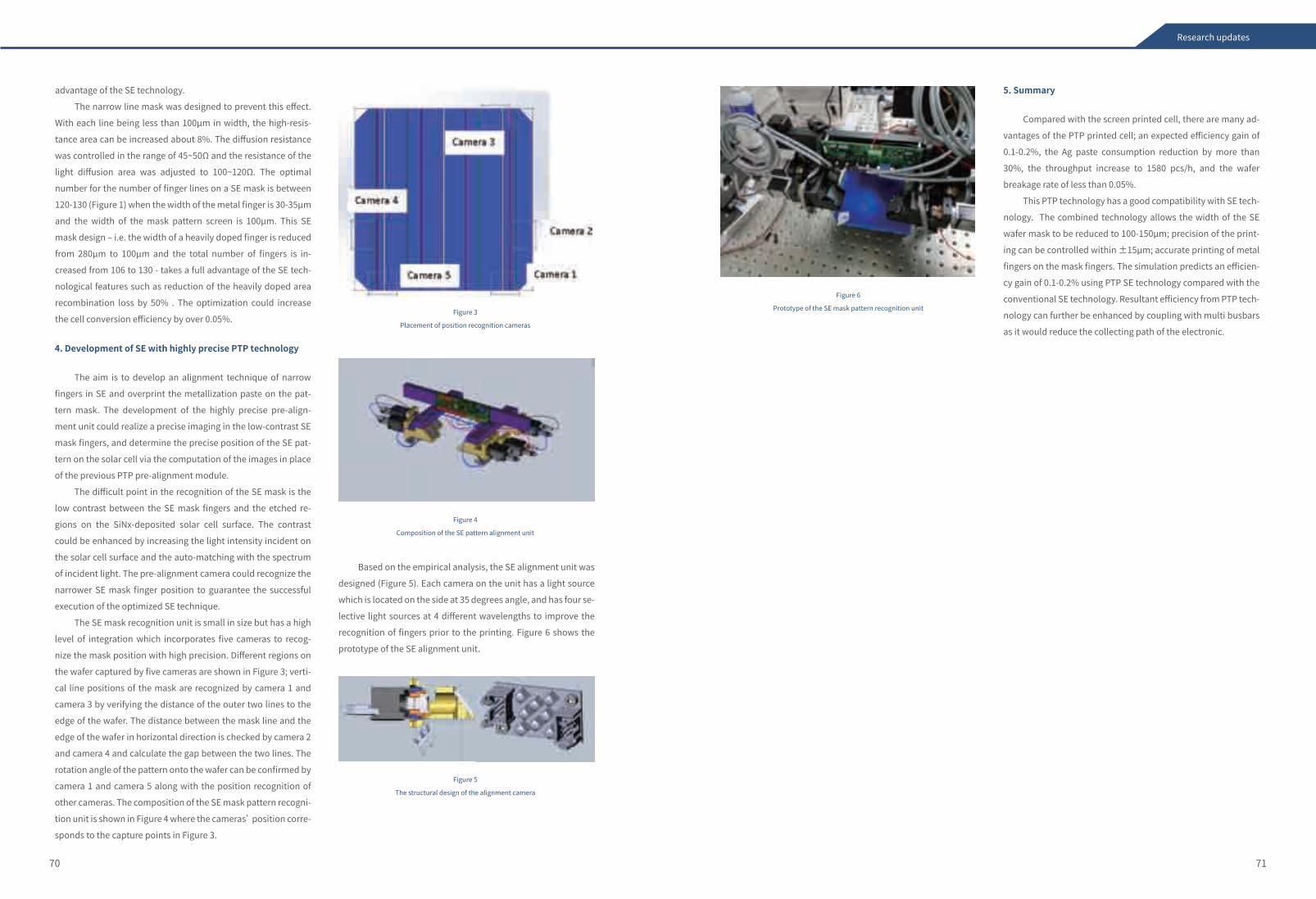
Compared with the screen printed cell, there are many ad-
vantages of the PTP printed cell; an expected efficiency gain of
0.1-0.2%, the Ag paste consumption reduction by more than
30%, the throughput increase to 1580 pcs/h, and the wafer
breakage rate of less than 0.05%.
This PTP technology has a good compatibility with SE tech-
nology. The combined technology allows the width of the SE
wafer mask to be reduced to 100-150µm; precision of the print-
ing can be controlled within ±15µm; accurate printing of metal
fingers on the mask fingers. The simulation predicts an efficien-
cy gain of 0.1-0.2% using PTP SE technology compared with the
conventional SE technology. Resultant efficiency from PTP tech-
nology can further be enhanced by coupling with multi busbars
as it would reduce the collecting path of the electronic.
5. Summary
70 71
Research updates
Figure 6
Prototype of the SE mask pattern recognition unit
advantage of the SE technology.
The narrow line mask was designed to prevent this effect.
With each line being less than 100μm in width, the high-resis-
tance area can be increased about 8%. The diffusion resistance
was controlled in the range of 45~50Ω and the resistance of the
light diffusion area was adjusted to 100~120Ω. The optimal
number for the number of finger lines on a SE mask is between
120-130 (Figure 1) when the width of the metal finger is 30-35μm
and the width of the mask pattern screen is 100μm. This SE
mask design ‒ i.e. the width of a heavily doped finger is reduced
from 280μm to 100μm and the total number of fingers is in-
creased from 106 to 130 - takes a full advantage of the SE tech-
nological features such as reduction of the heavily doped area
recombination loss by 50% . The optimization could increase
the cell conversion efficiency by over 0.05%.
The aim is to develop an alignment technique of narrow
fingers in SE and overprint the metallization paste on the pat-
tern mask. The development of the highly precise pre-align-
ment unit could realize a precise imaging in the low-contrast SE
mask fingers, and determine the precise position of the SE pat-
tern on the solar cell via the computation of the images in place
of the previous PTP pre-alignment module.
The difficult point in the recognition of the SE mask is the
low contrast between the SE mask fingers and the etched re-
gions on the SiNx-deposited solar cell surface. The contrast
could be enhanced by increasing the light intensity incident on
the solar cell surface and the auto-matching with the spectrum
of incident light. The pre-alignment camera could recognize the
narrower SE mask finger position to guarantee the successful
execution of the optimized SE technique.
The SE mask recognition unit is small in size but has a high
level of integration which incorporates five cameras to recog-
nize the mask position with high precision. Different regions on
the wafer captured by five cameras are shown in Figure 3; verti-
cal line positions of the mask are recognized by camera 1 and
camera 3 by verifying the distance of the outer two lines to the
edge of the wafer. The distance between the mask line and the
edge of the wafer in horizontal direction is checked by camera 2
and camera 4 and calculate the gap between the two lines. The
rotation angle of the pattern onto the wafer can be confirmed by
camera 1 and camera 5 along with the position recognition of
other cameras. The composition of the SE mask pattern recogni-
tion unit is shown in Figure 4 where the cameras’ position corre-
sponds to the capture points in Figure 3.
Based on the empirical analysis, the SE alignment unit was
designed (Figure 5). Each camera on the unit has a light source
which is located on the side at 35 degrees angle, and has four se-
lective light sources at 4 different wavelengths to improve the
recognition of fingers prior to the printing. Figure 6 shows the
prototype of the SE alignment unit.
4. Development of SE with highly precise PTP technology
Figure 3
Placement of position recognition cameras
Figure 4
Composition of the SE pattern alignment unit
Figure 5
The structural design of the alignment camera
73
Chapter 3 Testing Laboratory
The testing laboratory at the State Key Laboratory PV Science and Technol-ogy (SKL PVST) is comprised of character-ization, simulation, module and system testing divisions, and provides testing and characterization services to R&D groups and the manufacturing department.
Silicon wafers and solar cells, includ-ing half-finished solar cells, are character-ized in the characterization laboratory. Th-e simulation laboratory optimizes each pr-ocessing and characterization step involve-d in manufacturing a solar cell through simulation and analytical modelling, nam-ely, Centaurus TCAD and Quokka. The module testing laboratory evaluates mod-ule reliability and performance - 175 tests which include thermal and chemical analy-sis are conducted. The system testing labo-ratory provides system testing service and performance analysis to Trina Solar system owners and stakeholders.
◆ 3.1 c-Si Solar Cell Characterization & Simulation
◆ 3.2 PV Module Testing Laboratory
◆ 3.3 PV System Testing Laboratory
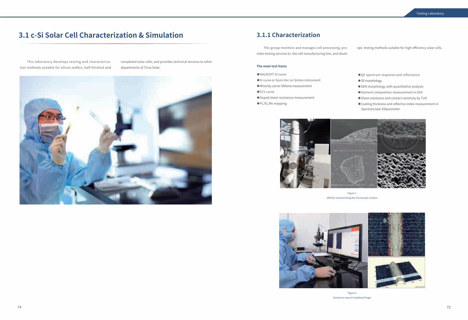
7574
Figure 2
Zata focus map of metallized finger
Figure 1
SEM for characterizing the microscopic surface
3.1 c-Si Solar Cell Characterization & Simulation 3.1.1 Characterization
The main test items
◆HALM/IVT-IV curve
◆IV curve or Suns-Voc on Sinton instrument
◆Minority carrier lifetime measurement
◆ECV curve
◆Doped sheet resistance measurement
◆PL/EL/Rs mapping
Testing Laboratory
◆QE spectrum response and reflectance
◆3D morphology
◆SEM morphology with quantitative analysis
◆Element composition measurement in EDX
◆Sheet resistance and contact resistivity by TLM
◆Coating thickness and reflective index measurement in Spectroscopic Ellipsometer
This laboratory develops testing and characteriza-
tion methods suitable for silicon wafers, half-finished and
completed solar cells, and provides technical services to other
departments of Trina Solar.
This group monitors and manages cell processing, pro-
vides testing services to the cell manufacturing line, and devel-
ops testing methods suitable for high-efficiency solar cells.
Module testing laboratory performs module reliability
tests and solar cell materials’ physical and chemical tests.
The laboratory has established a long-term strategic collabo-
ration with credible accreditation and testing institutions both
in China and overseas. Trina Solar was the first PV manufactur-
er to obtain UL CTDP (Client Test Data Program), and has also
obtained WTMP (Witness Testing at Manufacturer's Premises)
accreditation from TUV Rheinland, and the Golden Sun Certifi-
cate accreditation from CGC.
In 2016, the laboratory has successfully been re-certified
with CNAS, TUV-PTL, UL CTDP and WTMP. It also obtained CSA-
WMT and CTF from TUV Rheinland ‒ Trina Solar is the first PV
manufacturer to obtain this certification.
175 tests focusing on module reliability, thermal analysis
of PV materials, physical property of PV auxiliary materials, and
chemistry measurements are carried out.
TUV and UL qualifica-tion in 2010 as apart of WTDP
CNAS Accredi-tation in 2010, with 40 test items
Passed UL CTDP in 2012
TUV-PTL qualification in 2014; CNAS test items increased to 64
Passed CGC and WMT recertification, and get annual authorization by UL-CTDP, get authorization onoutdoor exposure test, hot spot endurance test,and bypassdiode thermalperformance test
CGC certificationin2011,becom-ing WTDP
Passed CNAS re-assessment in 2013 increasing to 49 testing item Passed CNAS re-assessment;obtain
TUV-CTF certification; obtain CSA-WMT certification; passed UL-CTDP annual assessment
2010 2011 2012 2013 2014 2015 2016
7776
3.1.2 Simulation
Optical, thermal and electrical characteristics of silicon
-based and compound solar cells are simulated in multi-dime-
nsions using Centaurus TCAD and Quokka - both empirical and
theoretical approaches are employed in developing a model.
The group provides theoretically optimized models/scenarios
to R&D groups, the pilot line and the manufacturing line within
Trina Solar. It employs an independently developed 3D opti-
cal simulation tool based on Centaurus TCAD and Monte Carlo
method; combined with QE spectral response and reflectance,
it is an effective characterization method in predicting the
short circuit current gain of an optically optimized processing
step. In Figure 3, the measured reflectance and the simulated
reflectance are compared and it demonstrates the proximity
of the theoretical simulation to the actual measurement.
3.2 Module Testing Laboratory
Figure 3
Independently developed 3D optical simulation tool
Figure 5
Electrical simulation based on SPICE method
Various models are built for different cell structures using
Centaurus TCAD and Quokka which significantly reduces the
modeling difficulty and simplifies parameter-setting steps. In
Centaurus TCAD, 2D and 3D models are constructed to describe
mechanisms of the carrier generation, transportation and re-
combination. The power loss analysis of a solar cell under vari-
ous operating conditions is the most useful aspect of the device
simulation as reducing these power losses would lead to overall
power gain in a solar cell.
Testing Laboratory
Figure 4
3D models created by Centaurus TCAD and Quokka, recombination
current analysis of a solar cell at various operating conditions
1.E-04
1.E-03
1.E-02
1.E-01
1.E+00
1.E+01
0.4 0.5 0.6 0.7
Curr
ent d
ensi
ty [
mA/
cm2]
Inner voltage [V]
Recombina�on currents - rear diffusions(s)
tot
SRH
Auger
rad
inac�ve P
rear cont
Vmpp
Voc
Electrical schematics and analysis of finger bars are car-
ried out using SPICE and nodal analysis. The nodal analysis
computes the power loss due to the series resistance using
the current flow rules in busbars and fingers. SPICE simulates a
solar cell circuit by creating a series of micro-units to verify cir-
cuit operation.
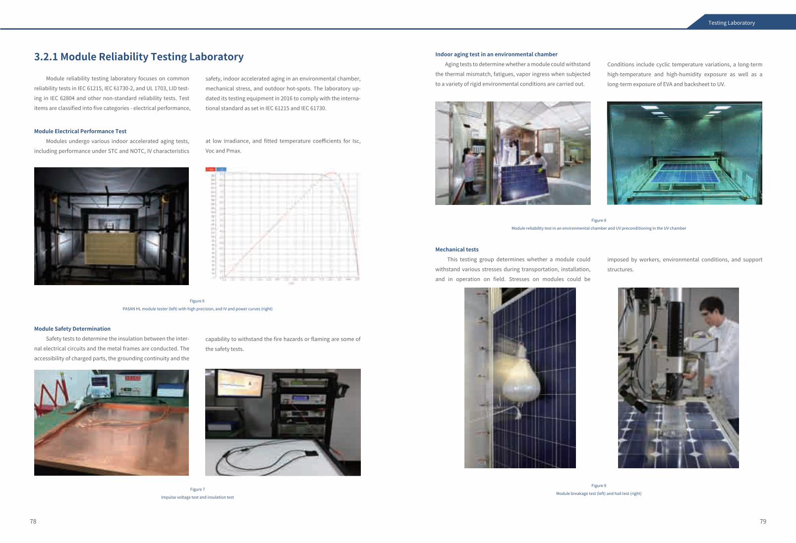
7978
Figure 6
PASAN HL module tester (left) with high precision, and IV and power curves (right)
Figure 8
Module reliability test in an environmental chamber and UV preconditioning in the UV chamber
Figure 7
Impulse voltage test and insulation test
Figure 9
Module breakage test (left) and hail test (right)
Testing Laboratory
Module Safety Determination
Safety tests to determine the insulation between the inter-
nal electrical circuits and the metal frames are conducted. The
accessibility of charged parts, the grounding continuity and the
capability to withstand the fire hazards or flaming are some of
the safety tests.
Indoor aging test in an environmental chamber
Aging tests to determine whether a module could withstand
the thermal mismatch, fatigues, vapor ingress when subjected
to a variety of rigid environmental conditions are carried out.
Mechanical tests
This testing group determines whether a module could
withstand various stresses during transportation, installation,
and in operation on field. Stresses on modules could be
imposed by workers, environmental conditions, and support
structures.
Conditions include cyclic temperature variations, a long-term
high-temperature and high-humidity exposure as well as a
long-term exposure of EVA and backsheet to UV. safety, indoor accelerated aging in an environmental chamber,
mechanical stress, and outdoor hot-spots. The laboratory up-
dated its testing equipment in 2016 to comply with the interna-
tional standard as set in IEC 61215 and IEC 61730.
at low irradiance, and fitted temperature coefficients for Isc,
Voc and Pmax.
Module Electrical Performance Test
Modules undergo various indoor accelerated aging tests,
including performance under STC and NOTC, IV characteristics
Module reliability testing laboratory focuses on common
reliability tests in IEC 61215, IEC 61730-2, and UL 1703, LID test-
ing in IEC 62804 and other non-standard reliability tests. Test
items are classified into five categories - electrical performance,
3.2.1 Module Reliability Testing Laboratory
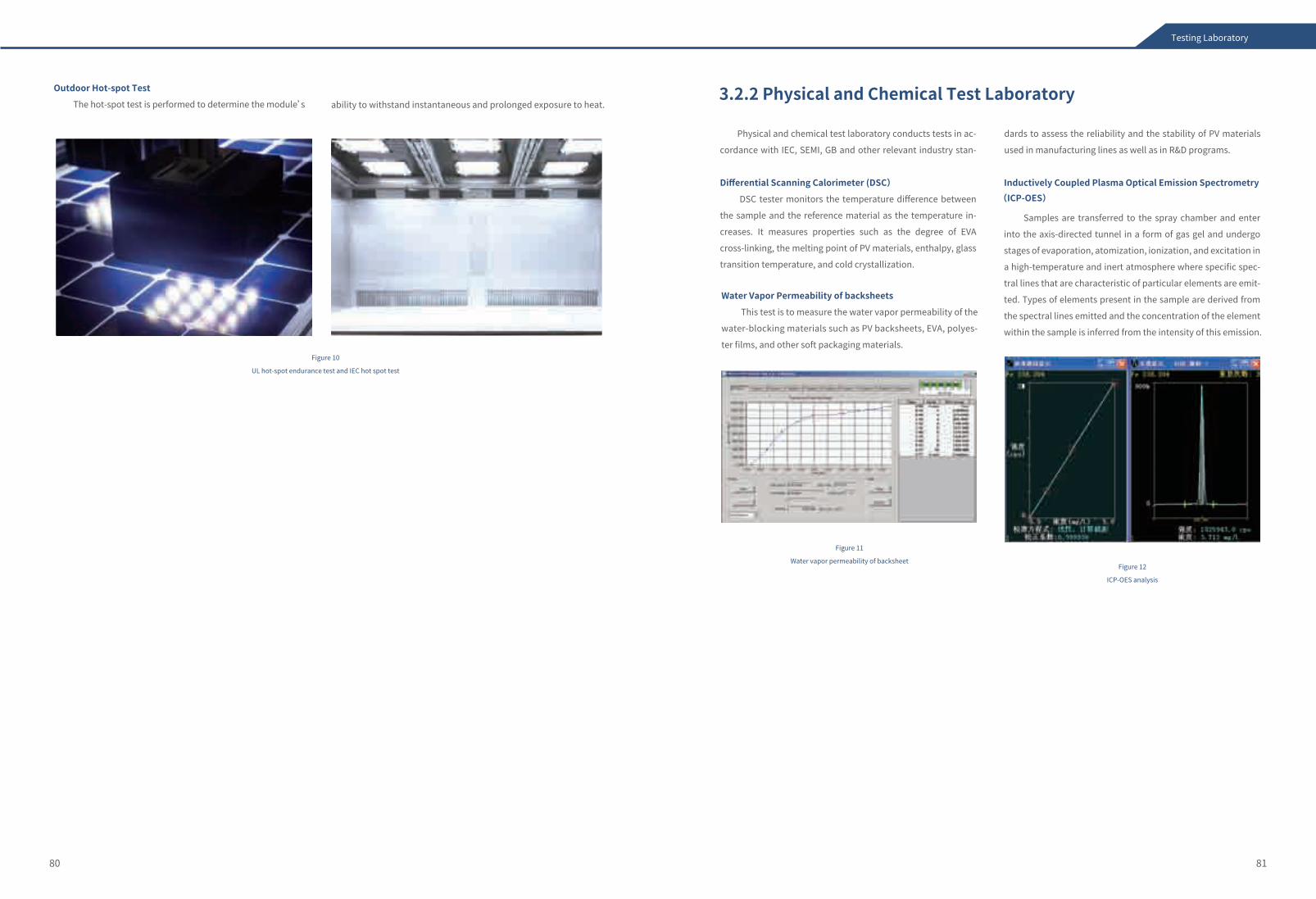
8180
Differential Scanning Calorimeter (DSC)
DSC tester monitors the temperature difference between
the sample and the reference material as the temperature in-
creases. It measures properties such as the degree of EVA
cross-linking, the melting point of PV materials, enthalpy, glass
transition temperature, and cold crystallization.
Water Vapor Permeability of backsheets
This test is to measure the water vapor permeability of the
water-blocking materials such as PV backsheets, EVA, polyes-
ter films, and other soft packaging materials.
Physical and chemical test laboratory conducts tests in ac-
cordance with IEC, SEMI, GB and other relevant industry stan-
dards to assess the reliability and the stability of PV materials
used in manufacturing lines as well as in R&D programs.
Figure 10
UL hot-spot endurance test and IEC hot spot test
Figure 12
ICP-OES analysis
Figure 11
Water vapor permeability of backsheet
Testing Laboratory
ability to withstand instantaneous and prolonged exposure to heat.
Samples are transferred to the spray chamber and enter
into the axis-directed tunnel in a form of gas gel and undergo
stages of evaporation, atomization, ionization, and excitation in
a high-temperature and inert atmosphere where specific spec-
tral lines that are characteristic of particular elements are emit-
ted. Types of elements present in the sample are derived from
the spectral lines emitted and the concentration of the element
within the sample is inferred from the intensity of this emission.
Inductively Coupled Plasma Optical Emission Spectrometry(ICP-OES)
3.2.2 Physical and Chemical Test Laboratory
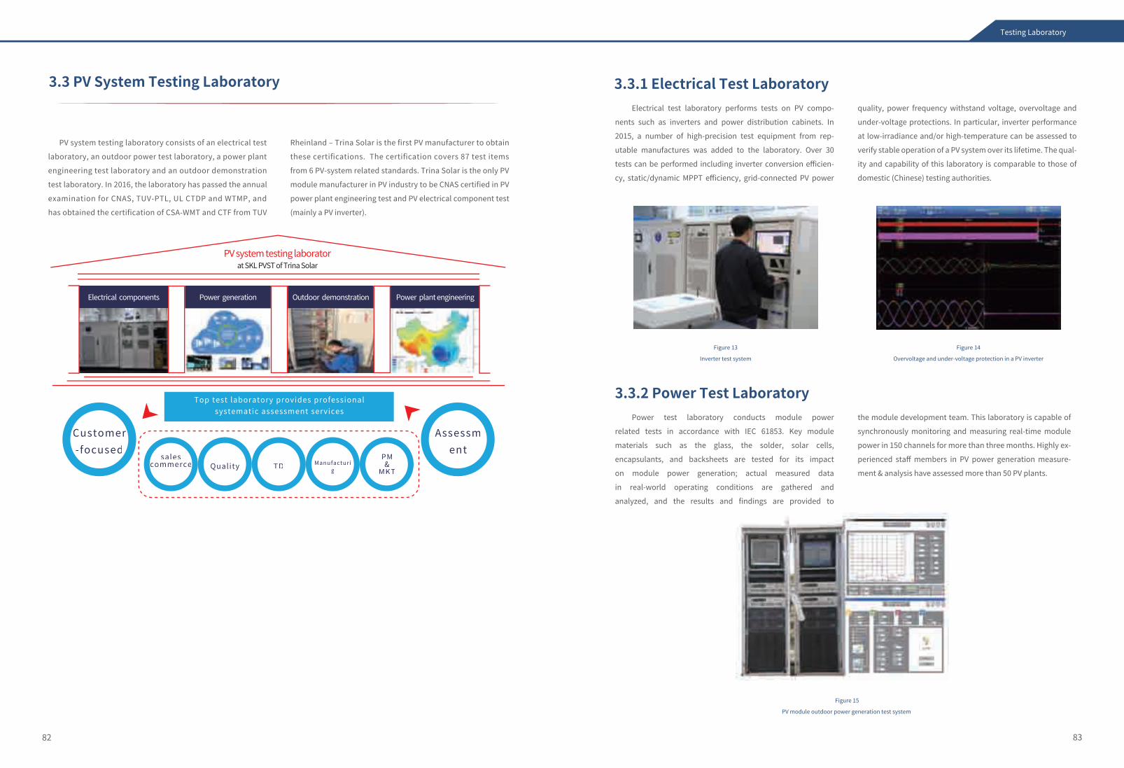
PV system testing laboratorat SKL PVST of Trina Solar
Electrical components Power generation Outdoor demonstration Power plant engineering
Top test laboratory provides professionalsystematic assessment services
Assessment
Customer-focused
salescommerce
PM&
MKTQuality TD Manufacturi
g
8382
Figure 14
Overvoltage and under-voltage protection in a PV inverter
Figure 13
Inverter test system
Figure 15
PV module outdoor power generation test system
3.3.1 Electrical Test LaboratoryElectrical test laboratory performs tests on PV compo-
nents such as inverters and power distribution cabinets. In
2015, a number of high-precision test equipment from rep-
utable manufactures was added to the laboratory. Over 30
tests can be performed including inverter conversion efficien-
cy, static/dynamic MPPT efficiency, grid-connected PV power
quality, power frequency withstand voltage, overvoltage and
under-voltage protections. In particular, inverter performance
at low-irradiance and/or high-temperature can be assessed to
verify stable operation of a PV system over its lifetime. The qual-
ity and capability of this laboratory is comparable to those of
domestic (Chinese) testing authorities.
3.3.2 Power Test LaboratoryPower test laboratory conducts module power
related tests in accordance with IEC 61853. Key module
materials such as the glass, the solder, solar cells,
encapsulants, and backsheets are tested for its impact
on module power generation; actual measured data
in real-world operating conditions are gathered and
analyzed, and the results and findings are provided to
the module development team. This laboratory is capable of
synchronously monitoring and measuring real-time module
power in 150 channels for more than three months. Highly ex-
perienced staff members in PV power generation measure-
ment & analysis have assessed more than 50 PV plants.
PV system testing laboratory consists of an electrical test
laboratory, an outdoor power test laboratory, a power plant
engineering test laboratory and an outdoor demonstration
test laboratory. In 2016, the laboratory has passed the annual
examination for CNAS, TUV-PTL, UL CTDP and WTMP, and
has obtained the certification of CSA-WMT and CTF from TUV
Rheinland ‒ Trina Solar is the first PV manufacturer to obtain
these certifications. The certification covers 87 test items
from 6 PV-system related standards. Trina Solar is the only PV
module manufacturer in PV industry to be CNAS certified in PV
power plant engineering test and PV electrical component test
(mainly a PV inverter).
3.3 PV System Testing Laboratory
Testing Laboratory
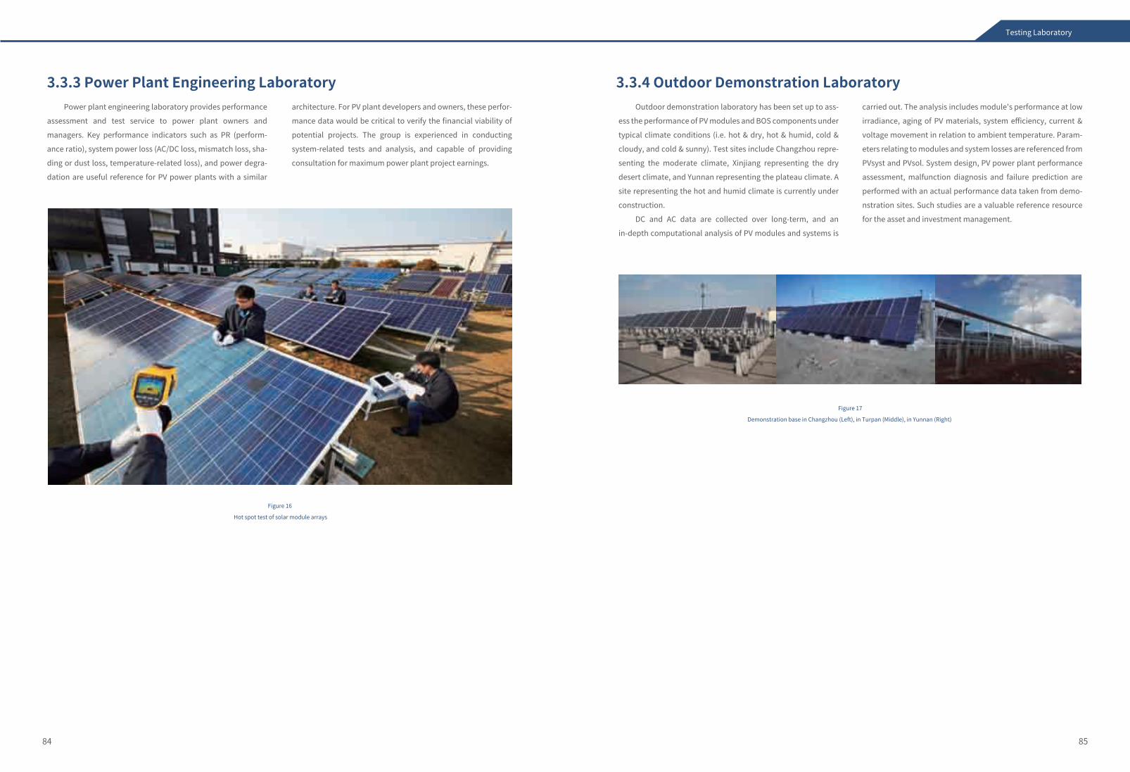
8584
Power plant engineering laboratory provides performance
assessment and test service to power plant owners and
managers. Key performance indicators such as PR (perform-
ance ratio), system power loss (AC/DC loss, mismatch loss, sha-
ding or dust loss, temperature-related loss), and power degra-
dation are useful reference for PV power plants with a similar
architecture. For PV plant developers and owners, these perfor-
mance data would be critical to verify the financial viability of
potential projects. The group is experienced in conducting
system-related tests and analysis, and capable of providing
consultation for maximum power plant project earnings.
3.3.3 Power Plant Engineering Laboratory
Figure 16
Hot spot test of solar module arrays
Figure 17
Demonstration base in Changzhou (Left), in Turpan (Middle), in Yunnan (Right)
3.3.4 Outdoor Demonstration LaboratoryOutdoor demonstration laboratory has been set up to ass-
ess the performance of PV modules and BOS components under
typical climate conditions (i.e. hot & dry, hot & humid, cold &
cloudy, and cold & sunny). Test sites include Changzhou repre-
senting the moderate climate, Xinjiang representing the dry
desert climate, and Yunnan representing the plateau climate. A
site representing the hot and humid climate is currently under
construction.
DC and AC data are collected over long-term, and an
in-depth computational analysis of PV modules and systems is
carried out. The analysis includes module's performance at low
irradiance, aging of PV materials, system efficiency, current &
voltage movement in relation to ambient temperature. Param-
eters relating to modules and system losses are referenced from
PVsyst and PVsol. System design, PV power plant performance
assessment, malfunction diagnosis and failure prediction are
performed with an actual performance data taken from demo-
nstration sites. Such studies are a valuable reference resource
for the asset and investment management.
Testing Laboratory
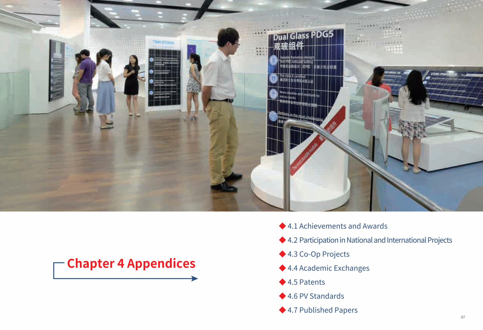
87
Chapter 4 Appendices
◆ 4.1 Achievements and Awards
◆ 4.2 Participation in National and International Projects
◆ 4.3 Co-Op Projects
◆ 4.4 Academic Exchanges
◆ 4.5 Patents
◆ 4.6 PV Standards
◆ 4.7 Published Papers
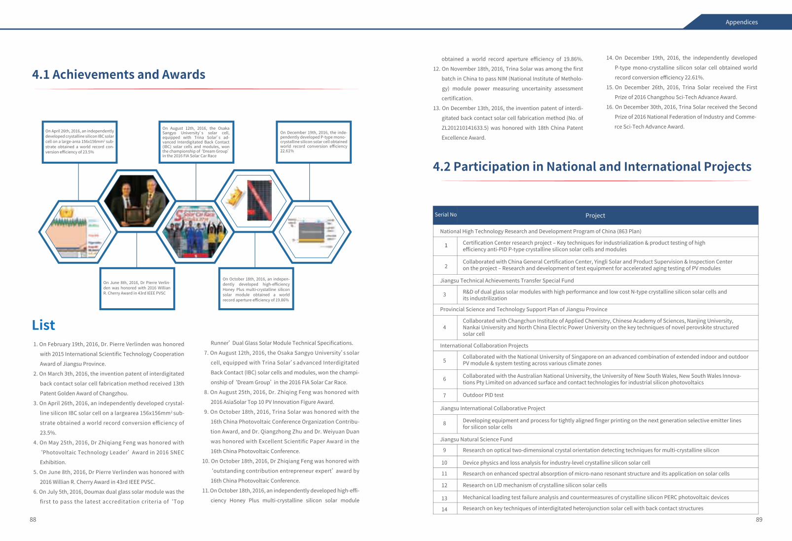
On April 26th, 2016, an independently developed crystalline silicon IBC solar cell on a large-area 156x156mm2 sub-strate obtained a world record con-version efficiency of 23.5%
On June 8th, 2016, Dr Pierre Verlin-den was honored with 2016 Willian R. Cherry Award in 43rd IEEE PVSC
On October 18th, 2016, an indepen-dently developed high-efficiency Honey Plus multi-crystalline silicon solar module obtained a world record aperture efficiency of 19.86%
On August 12th, 2016, the Osaka Sangyo University’s solar cell, equipped with Trina Solar’s ad-vanced Interdigitated Back Contact (IBC) solar cells and modules, won the championship of ‘Dream Group’ in the 2016 FIA Solar Car Race
On December 19th, 2016, the inde-pendently developed P-type mono-crystalline silicon solar cell obtained world record conversion efficiency 22.61%
8988
Appendices
4.1 Achievements and Awards
4.2 Participation in National and International Projects
Serial No
National High Technology Research and Development Program of China (863 Plan)
Project
Collaborated with China General Certification Center, Yingli Solar and Product Supervision & Inspection Center on the project ‒ Research and development of test equipment for accelerated aging testing of PV modules
Certification Center research project ‒ Key techniques for industrialization & product testing of high efficiency anti-PID P-type crystalline silicon solar cells and modules
1
2
R&D of dual glass solar modules with high performance and low cost N-type crystalline silicon solar cells and its industrilization
Collaborated with Changchun Institute of Applied Chemistry, Chinese Academy of Sciences, Nanjing University, Nankai University and North China Electric Power University on the key techniques of novel perovskite structured solar cell
Collaborated with the National University of Singapore on an advanced combination of extended indoor and outdoor PV module & system testing across various climate zones
Collaborated with the Australian National University, the University of New South Wales, New South Wales Innova-tions Pty Limited on advanced surface and contact technologies for industrial silicon photovoltaics
Outdoor PID test
Research on enhanced spectral absorption of micro-nano resonant structure and its application on solar cells
Research on LID mechanism of crystalline silicon solar cells
Jiangsu Technical Achievements Transfer Special Fund
Provincial Science and Technology Support Plan of Jiangsu Province
International Collaboration Projects
Jiangsu International Collaborative Project
Jiangsu Natural Science Fund
3
4
5
7
6
8
9
10
11
12
Mechanical loading test failure analysis and countermeasures of crystalline silicon PERC photovoltaic devices13
Research on key techniques of interdigitated heterojunction solar cell with back contact structures14
Developing equipment and process for tightly aligned finger printing on the next generation selective emitter linesfor silicon solar cells
Research on optical two-dimensional crystal orientation detecting techniques for multi-crystalline silicon
Device physics and loss analysis for industry-level crystalline silicon solar cell
1. On February 19th, 2016, Dr. Pierre Verlinden was honored
with 2015 International Scientific Technology Cooperation
Award of Jiangsu Province.
2. On March 3th, 2016, the invention patent of interdigitated
back contact solar cell fabrication method received 13th
Patent Golden Award of Changzhou.
3. On April 26th, 2016, an independently developed crystal-
line silicon IBC solar cell on a largearea 156x156mm2 sub-
strate obtained a world record conversion efficiency of
23.5%.
4. On May 25th, 2016, Dr Zhiqiang Feng was honored with
‘Photovoltaic Technology Leader’ Award in 2016 SNEC
Exhibition.
5. On June 8th, 2016, Dr Pierre Verlinden was honored with
2016 Willian R. Cherry Award in 43rd IEEE PVSC.
6. On July 5th, 2016, Doumax dual glass solar module was the
first to pass the latest accreditation criteria of ‘Top
Runner’ Dual Glass Solar Module Technical Specifications.
7. On August 12th, 2016, the Osaka Sangyo University’s solar
cell, equipped with Trina Solar’s advanced Interdigitated
Back Contact (IBC) solar cells and modules, won the champi-
onship of ‘Dream Group’ in the 2016 FIA Solar Car Race.
8. On August 25th, 2016, Dr. Zhiqing Feng was honored with
2016 AsiaSolar Top 10 PV Innovation Figure Award.
9. On October 18th, 2016, Trina Solar was honored with the
16th China Photovoltaic Conference Organization Contribu-
tion Award, and Dr. Qiangzhong Zhu and Dr. Weiyuan Duan
was honored with Excellent Scientific Paper Award in the
16th China Photovoltaic Conference.
10. On October 18th, 2016, Dr Zhiqiang Feng was honored with
‘outstanding contribution entrepreneur expert’ award by
16th China Photovoltaic Conference.
11. On October 18th, 2016, an independently developed high-effi-
ciency Honey Plus multi-crystalline silicon solar module
obtained a world record aperture efficiency of 19.86%.
12. On November 18th, 2016, Trina Solar was among the first
batch in China to pass NIM (National Institute of Metholo-
gy) module power measuring uncertainity assessment
certification.
13. On December 13th, 2016, the invention patent of interdi-
gitated back contact solar cell fabrication method (No. of
ZL201210141633.5) was honored with 18th China Patent
Excellence Award.
14. On December 19th, 2016, the independently developed
P-type mono-crystalline silicon solar cell obtained world
record conversion efficiency 22.61%.
15. On December 26th, 2016, Trina Solar received the First
Prize of 2016 Changzhou Sci-Tech Advance Award.
16. On December 30th, 2016, Trina Solar received the Second
Prize of 2016 National Federation of Industry and Comme-
rce Sci-Tech Advance Award.
List
held in Kuala Lumpur of Malaysia, and delivered a presentation of The Prospect of Mass-Produced MultiCrystalline Cells above 20% Efficiency: How High Can p-TypeMultiGo?.
From April 5th to 10th , 2016, Dr Pierre Verlinden, Guanchao Xu and Feng Ye attened 43rd Photovoltaic Specialists Conference, Dr. Pierre Verlinden delivereda presentation on Mass Production of High-Efficiency p-Type PERC Solar Cell: How High Can p-Type Multi Go’, and 40 Years of Development of IBC Silicon Solar Cells. Why Is It Taking So Long?, and was honored with William R. Cherry Award. Guanchao Xu delivered a presen-tation on 6 Inch IBC Cells with Efficiency of 23.5% Fabricated with Low-Cost Industrial Technologies and Feng Ye delivered a presentation on 22.13% Efficient Industrial p-Type Mono PERC Solar Cell.
On June 17th, 2016, Dr. Pierre Verlinden visited Ohio State University, and delivered a presentation on 21.25% World Efficiency Record with Multi-Crystalline p-Type Silicon Solar Cells: Closing the Gap with n-Type Mono.
From June 20th to 24th , 2016, Dr Pierre Verlinden, Dr Wei-yuan Duan, Zhonglan Li, Shengcheng Zhang, Shu Zhang, Huijun Zhu and Jing Mao attended 32rd European Photovoltaic Solar Energy Conference. Dr Pierre Verlinden delivered a presentation on ‘Perspectives for Cost Decline in the PV Industry’ in IEA PVPS Task1, Weiyuan Duan delivered a presentation on A Route towards High Efficiency n-type PERT Solar Cells, Zhonglan Li delivered a presentation on Pilot Production of 6’’ IBC Solar Cells Yielding A Median Efficiency of 23% with A Low-Cost Industrial Process, Shu Zhang delivered a presentation on Low Temperature Conductive Film (CF) Interconnection Process for PV Modules.
From August 25th to 26th, 2016, Dr. Zhiqiang Feng, Jianmei Xu and Yue Zong attended Asia Solar Energy Photovoltaic Exhibit, Dr. Zhiqiang Feng was honored with 2016 AsiaSolar Top 10 PV Innovation Figure Award, Jianmei Xu delivered a presentation on Technological Innovation Promoting the Devel-opment of Optimal Photovoltaic Products and the Industry Development.
From September 5th to 10th, 2016, Dr Zhen Zhang attended 2016 Photovoltaic Conference ‒ PV World Forum held in Korea, and delivered a presentation on High Performance Crystalline Silicon Solar Cell and Module Products. From September 26th to October 1st, 2016, Dr Yifeng Chen attendedBifacial Workshop held in Japan, and delivered a presentation
9190
From January 28th to 29th, 2016, Dr. Pierre Verlinden at-tended 12th Workshop on the Future Direction of Photovoltaics held in Tokyo Institute of Technology, Japan, and delivered a presentation on ‘Challenges and Opportunities of High-Perfor-mance Solar Cells and PV Modules in Large Volume Production’.
On February 23st, Jianmei Xu attended the workshop of National Renewable Energy Laboratory in US, and delivered a presentation on The Reliability of Dual-Glass Module Designed for Harsh Climates.
From February 27th to March 5th, 2016, Dr Zhiqiang Feng
Appendices
4.3 Achievements and Awards
4.4 Academic Exchanges
The laboratory promotes and encourages academic collaborations and exchanges. Funds for such co-op projects are available to attract PV talents and to accelerate the technical development. Current five co-op projects focusing on the fundamental physics of PV science and technology, and promotion of PV industry are as follows.
Serial No Project
Serial No
The actual power generation of PV systems from the Solar Energy Research Institute of Shunde, Sun Yat-sen University
The impact of rooftop PV arrays on the energy consumption of a building in South Jiangsu from Hohai University1
2
Plug-and-play household PV systems from HeFei University of Technology
Structures and degradation mechanisms of a biomimetic anti-reflective (ARC) self-cleaning glass from Changzhou University
Power generation of dual glass PV modules from Hohai University
3
4
5
R&D on N-type mono-crystalline high-efficiency solar cells and its industrilization
Changzhou Technical Achievements Transfer and Industrialization Plans
15
attended 2016 PV EXPO conference held in Tokyo, and delivered a presentation on High-Efficiency and High-Reliability Anti-PID Solar Cells and Solar Modules.
From March 4th to 12th, 2016, Dr Pierre Verlinden, Weiwei Deng and Wenhao Cai attended 2016 SiliconPV Photovoltaic Workshop, Weiwei Deng delivered a presentation on Develop-ment of High-efficiency Industrial p-type Multi-crystalline PERC Solar Cells with Efficiency Greater than 21%.
From March 16th to 17th , 2016, Dr Pierre Verlinden was in-vited to attend Photovoltaic Solar Cell Technology Conference
From September 29th to October 1st, 2016, Guanchao Xu was invited to attend 2016 Photovoltaic Industry Workshop held in Sungkyunkwan University in Korea, and delivered a presenta-tion on High Efficiency Approach in Trina Solar.
From October 1st to 7th, Hui Shen attended SAYURI-PV 2016 Workshop held in Japan, and delivered a presentation on Opportunity and Challenge: >21% Large-Area n-Type PERT Bifa-cial Solar Cells in Research and Production.
From October 8th to 16th, Shuya Ye attended 9th Interna-tional Crystalline Silicon Solar Cell Workshop & 3rd Silicon Mate-rial Workshop, and delivered a presentation on The Numerical Simulation of Silicon-Crystalline Growth.
From October 14th to 18th, Dr Zhiqiang Feng, Dr Pierre Ver-linden, Dr Zhen Zhang, Dr Zhen Xiong, Dr Qiangzhong Zhu, Dr Weiyuan Duan and et al (17 attendees in total) attended 16th China Photovoltaic Conference (CPVC16), Trina Solar was hon-ored with Organizational Contribution Award, Dr Qiangzhong Zhu and Dr Weiyuan Duan were honored with Excellent Scientif-ic Paper Award, Dr Zhen Xiong, Dr Yifeng Chen and other 12 at-tendees delivered 14 presentations.
On October 29th, Dr Zhiqiang Feng and Dr Pierre Verlinden attended 3rd Asia Photovoltaic Exhibit held in Singapore, Dr Zhiqiang Feng delivered a presentation of Multi-crystalline Sili-con Solar Module with Aperture Efficiency of 19.86%, Dr Pierre Verlinden delivered a presentation on Will We Have > 22% Effi-cient Multi-Crystalline p-Type Silicon Solar Cells?.
From October 19th to 21th, Dr Zhiqiang Feng and Dr Pierre Verlinden attended China Photovoltaic Conference & Exhibit held in Beijing, Dr Zhiqiang Feng delivered a presentation on The PERC Solar Cell Technology from Laboratory to Industrial-ization, Dr Pierre Verliden delivering a presentation on Will We Have > 22% Efficient Multi-Crystalline p-Type Silicon Solar Cells?.
On November 25th, Dr Zhiqiang Feng, Jianmei Xu, Dr Qiangzhong Zhu and et al attended 12th China SoG Silicon and PV Power Conference (CSPV), and delivered a series of presenta-tion.
Project
92 93
Appendices
4.5 Patents
In 2016, 106 patents were filed. 3 were Patent Cooperation Treaty (PCT), and 48 were invention patents. 97 pat-ents were approved this year, of which 38 patents were invention patents.
Cumulatively, as of December, 2016, 1317 patents have been filed by Trina Solar and of those, 597 were invention patents. With 747 valid patents and 220 valid invention patents, Trina Solar still holds the leading position amongst Chinese PV companies in number of valid invention patents held.
No. Invention Title Invention No. Authorized date
Sheet metal battery positive electrode printing method and printing apparatus
Method of preventing harmful polarization of crystalline silicon solar modules and the black line phenomenon occurs
Heterojunction solar cell and preparation method selective emitter
Upper and lower electrode structures of solar cells
A power differential PV maximum power point tracking method based on
Renewable Energy-powered street light system
Full back electrode of the solar cell and method of making the whole back electrode of solar cell
Volume resistivity and sheet resistance of the converter calibration device and calibration method
A photovoltaic roofing assembly structure and mounting structure
A method of increasing the emitter system selection process method using a mask width
Folding assembly
Improve the boron-doped P-type silicon solar cell apparatus and methods of using light-induced attenuation
Local solar cell doping methods
A poppet photovoltaic cells parallel resistance method
Heterojunction cells helps to reduce the number of positive gate line and its preparation method
Micro-concentrating photovoltaic solder strip
N-type doped polycrystalline silicon hydrogen passivation of heterojunction solar cell device
Silicon etching and wet etching equipment
ZL201410021773.8
ZL201210293067.X
ZL201410217097.1
ZL201210524975.5
ZL201410476803.4
ZL201310631186.6
ZL201310635112.X
ZL201410217300.5
ZL201310260249.1
ZL201410158537.0
ZL201210134804.1
ZL201410447653.4
ZL201410277487.8
ZL201310260236.4
ZL201410393187.6
ZL201310358556.3
ZL201310154476.6
ZL201410075181.4
2016/01/13
2016/01/20
2016/01/20
2016/02/10
2016/02/10
2016/03/02
2016/03/02
2016/03/23
2016/04/06
2016/04/06
2016/04/06
2016/04/06
2016/05/11
2016/05/25
2016/05/25
2016/06/15
2016/06/29
2016/07/13
1
2
3
4
5
6
7
8
9
10
11
12
13
14
15
16
17
18
No. Invention Title Invention No. Authorized date
PV modules with no cracked automatically split box method
A photovoltaic module frame marking method and photovoltaic module production technology
Photovoltaic confluence device additionally with anti-PID function
Implementation N-type crystalline silicon solar cell, the selective emitter structure
A photovoltaic system efficiency abnormality alarm method to judge
Crystalline silicon solar cell wet chemical treatment methods Texturing and cleaning step-wise
Solar cell and preparation method back laminated film passivation
Efficient polycrystalline ingot seed preparation method
PV modules with no cracked automatically split box method
Back symmetrical emitter heterojunction solar cells and preparation method
Seed silicon crystal orientation detection method and detection device
Solar cell device structure and preparation method has point contact structure
Heat radiation structure of photovoltaic intelligent junction box
Solar cell front electrode structure
Color photovoltaic module for building interior decoration and a preparation method thereof
Self - Aligned Selective Diffusion of Solar Cell Formation
Solar module mounting clamping device
Multi-overprinting alignment method for solar cell surface fine grid
Secondary printing alignment method of silicon solar cell
Solar cell sheet electric sheet-splitting device
ZL201210205461.3
ZL201310403033.6
ZL201410216834.6
ZL201410275382.9
ZL201410456746.3
ZL201410722696.9
ZL201310179373.5
ZL201410337376.1
ZL201210206152.8
ZL201310632740.2
ZL201410146800.4
ZL201410712128.0
ZL201510065118.7
ZL201410042618.4
ZL201410743903.9
ZL201410789712.6
ZL201310197268.4
ZL201410098396.8
ZL201310604369.9
ZL201310222931.1
2016/08/10
2016/08/17
2016/08/17
2016/08/17
2016/08/17
2016/08/17
2016/08/24
2016/08/24
2016/09/07
2016/09/07
2016/09/07
2016/09/07
2016/09/07
2016/09/28
2016/09/28
2016/09/28
2016/11/09
2016/11/16
2016/11/23
2016/12/28
19
20
21
22
23
24
25
26
27
28
29
30
31
32
33
34
35
36
37
38
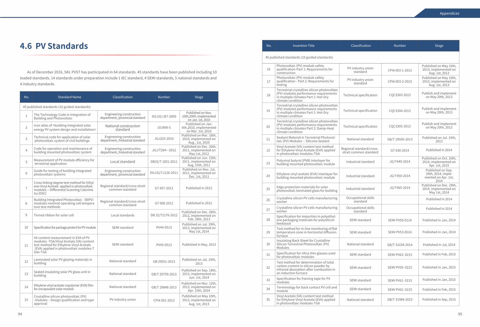
94 95
Appendices
The Technology Code in Integration ofBuilding and Photovoltaic
Icon atlas of <building integrated solar energy PV system design and installation>
Technical code for application of solar photovoltaic system of civil buildings
Code for operation and maintenance of building mounted photovoltaic system
Measurement of PV module efficiency for terrestrial application
Guide for testing of building integrated photovoltaic systems
Cross-linking degree test method for Ethylene-Vinyl Acetate applied in photovoltaic modules —Differential Scanning Calorimetry (DSC)
Building Integrated Photovoltaic(BIPV) modules nominal operating cell temperature test methods
Tinned ribbon for solar cell
Specification for package protect for PV module
VA content measurement in EVA of PV modules -TGA/Vinyl Acetate (VA) content test method for Ethylene-Vinyl Acetate (EVA) applied in photovoltaic modules-TGAs-TGA
Laminated solar PV glazing materials in building
Sealed insulating solar PV glass unit in building
Ethylene-vinyl acetate copolymer (EVA) film for encapsulant solar module
Crystalline silicon photovoltaic (PV) modules ‒ Design qualification and type approval
Engineering construction department, /provincial standard
National construction standard
Engineering construction department, /Industrial standard
Engineering construction department, /Industrial standard
Local standard
Engineering construction department, /provincial standard
Regional standard/cross-strait common standard
Regional standard/cross-strait common standard
Local standards
SEMI standard
SEMI standard
National standard
National standard
National standard
PV industry union
DGJ32/J87-2009
10J908-5
JGJ203-2010
JGJ/T264—2012
DB32/T 1831-2011
DGJ32/TJ126-2011
GT 007-2012
GT 008-2012
DB 32/T2176-2012
PV44-0513
PV45-0513
GB 29551-2013
GB/T 29759-2013
GB/T 29848-2013
CPIA 001-2013
Published on Nov. 10th,2009, implemented
on Jan. 1st, 2010Published on Jan.
6th,2010, implemented on Mar. 1st, 2010
Published on Mar. 18th, 2010, implemented on
Aug., 1st, 2010Published on Dec. 26th, 2011, implemented on
May 1st, 2012Published on Jun. 15th, 2011, implemented on
Aug. 15th, 2011Published on Nov. 1st, 2011, implemented on
Dec. 1st, 2011
Published in 2012
Published in 2012
Published on Dec. 28th, 2012, implemented on
Feb. 28th, 2013Published on Jul. 19th, 2013, implemented on
May 1st, 2014
Published in May, 2013
Published on Jul. 19th, 2013
Published on Sep. 18th, 2013, implemented on
Jun. 1st, 2014
Published on Nov. 12th, 2013, implemented on
Apr. 15th, 2014Published on May 10th, 2013, implemented on
Aug. 1st, 2013
45 published standards (10 guided standards)
1
2
3
4
5
6
7
8
9
10
11
12
13
14
15
No. Standard Name Classification Number Stage
Invention Title Classification Number StageNo.
34
35
PV industry union standard
PV industry union standard
Technical specification
Technical specification
Technical specification
National standard
Regional standard/cross-strait common standard
Industrial standard
Industrial standard
Industrial standard
Occupational skills standard
Occupational skills standard
SEMI standard
SEMI standard
National standard
SEMI standard
SEMI standard
SEMI standard
SEMI standard
National standard
Photovoltaic (PV) module safety qualification-Part 1: Requirements for constructionPhotovoltaic (PV) module safety qualification - Part 2: Requirements for testingTerrestrial crystalline silicon photovoltaic (PV) modules performance requirements in multiple climates Part 1: Hot-Dry climate conditionTerrestrial crystalline silicon photovoltaic (PV) modules performance requirements in multiple climates Part 1: Hot-Dry climate conditionTerrestrial crystalline silicon photovoltaic (PV) modules performance requirements in multiple climates Part 2: Damp-Heat climate conditionSealant Material in Terrestrial Photovol-taic (PV) Modules -- Silicone SealantVinyl Acetate (VA) content test method for Ethylene-Vinyl Acetate (EVA) applied in photovoltaic modules-TGA
Polyvinyl butyral (PVB) interlayer for building mounted photovoltaic module
Ethylene vinyl acetate (EVA) interlayer for building mounted photovoltaic module
Edge protection materials for solar photovoltaic laminated glass for building
Crystalline silicon PV cells manufacturing worker
Crystalline silicon PV cells manufacturing workerSpecification for impurities in polyethyl-ene packaging materials for polysilicon feedstockTest method for in-line monitoring of flat temperature zone in horizontal diffusion furnaceInsulating Back Sheet for Crystalline Silicon Terrestrial Photovoltaic (PV) ModulesSpecification for Ultra-thin glasses used for photovoltaic modulesTest method for determination of total carbon content in silicon powder by infrared absorption after combustion in an induction furnaceSpecification for framing tape for PV modulesTerminology for back contact PV cell and moduleVinyl Acetate (VA) content test method for Ethylene-Vinyl Acetate (EVA) applied in photovoltaic modules-TGA
CPIA 003-1-2013
CPIA 003-2-2013
CQC3303-2013
CQC3304-2013
CQC3305-2013
GB/T 29595-2013
GT 030-2014
JG/T449-2014
JG/T450-2014
JG/T465-2014
SEMI PV50-0114
SEMI PV53-0514
GB/T 31034-2014
SEMI PV63- 0215
SEMI PV59- 0215
SEMI PV61- 0215
SEMI PV62- 0215
GB/T 31984-2015
Published on May 10th, 2013, implemented on
Aug. 1st, 2013Published on May 10th, 2013, implemented on
Aug. 1st, 2013
Publish and implement on May 20th, 2013
Publish and implement on May 20th, 2013
Publish and implement on May 20th, 2013
Published on Jul. 19th, 2013
Published in 2014
Published on Oct. 20th, 2014, implemented on
Apr. 1st, 2015Published on Sep. 29th, 2014, imple-
mented on Apr. 1st, 2014
Published on Dec. 29th, 2014, implemented on
May 1st, 2014
Published in 2014
Published in 2014
Published in Jan, 2014
Published in Jan, 2014
Published in Jul, 2014
Published in Feb, 2015
Published in Jan, 2015
Published in Jan, 2015
Published in Feb, 2015
Published in Sep, 2015
16
17
18
27
28
29
30
31
32
33
24
25
26
21
19
20
23
22
45 published standards (10 guided standards)
4.6 PV Standards
As of December 2016, SKL PVST has participated in 64 standards. 45 standards have been published including 10 leaded standards. 14 standards under preparation include 1 IEC standard, 4 SEMI standards, 5 national standards and 4 industry standards.
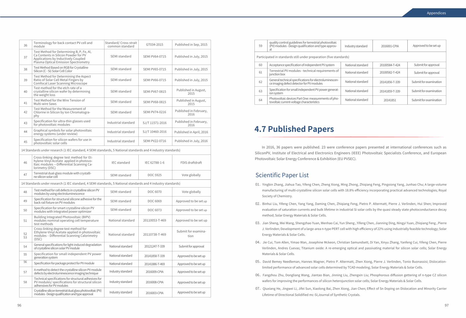
96 97
Appendices
4.7 Published Papers
In 2016, 36 papers were published. 23 were conference papers presented at international conferences such as SiliconPV, Institute of Electrical and Electronics Engineers (IEEE) Photovoltaic Specialists Conference, and European Photovoltaic Solar Energy Conference & Exhibition (EU PVSEC).
01.Yingbin Zhang, Jiahua Tao, Yifeng Chen, Zheng Xiong, Ming Zhong, Zhiqiang Feng, Pingxiong Yang, Junhao Chu; A large-volume
manufacturing of multi-crystalline silicon solar cells with 18.8% efficiency incorporating practical advanced technologies; Royal
Society of Chemistry.
02.Binhui Liu, Yifeng Chen, Yang Yang, Daming Chen, Zhiqiang Feng, Pietro P. Altermatt, Pierre J. Verlinden, Hui Shen; Improved
evaluation of saturation currents and bulk lifetime in industrial Si solar cells by the quasi steady state photoconductance decay
method; Solar Energy Materials & Solar Cells.
03.Jian Sheng, Wei Wang, Shengzhao Yuan, Wenhao Cai, Yun Sheng , Yifeng Chen, Jianning Ding, Ningyi Yuan, Zhiqiang Feng , Pierre
J. Verlinden; Development of a large-area n-type PERT cell with high efficiency of 22% using industrially feasible technology; Solar
Energy Materials & Solar Cells.
04.Jie Cui, Tom Allen, Yimao Wan, Josephine Mckeon, Christian Samundsett, Di Yan, Xinyu Zhang, Yanfeng Cui, Yifeng Chen, Pierre
Verlinden, Andres Cuevas; Titanium oxide: A re-emerging optical and passivating material for silicon solar cells; Solar Energy
Materials & Solar Cells.
05.David Bemey Needleman, Hannes Wagner, Pietro P. Altermatt, Zhen Xiong, Pierre J. Verlinden, Tonio Buonassisi; Dislocation-
limited performance of advanced solar cells determined by TCAD modeling; Solar Energy Materials & Solar Cells.
06.Fangzhou Zhu, Dongliang Wang, Jiantao Bian, Jinning Liu, Zhengxin Liu; Phosphorous diffusion gettering of n-type CZ silicon
wafers for improving the performances of silicon heterojunction solar cells; Solar Energy Materials & Solar Cells.
07.Qiuxiang He, Jingwei Li, Jifei Sun, Xiaolong Bai, Zhen Xiong, Jian Chen; Effect of Sn Doping on Dislocation and Minority Carrier
Lifetime of Directional Solidified mc-Si;Journal of Synthetic Crystals.
Scientific Paper List
PV industry union standard
PV industry union standard
Technical specification
Technical specification
Technical specification
National standard
Regional standard/cross-strait common standard
Industrial standard
Industrial standard
Industrial standard
Occupational skills standard
Occupational skills standard
SEMI standard
SEMI standard
National standard
SEMI standard
SEMI standard
SEMI standard
SEMI standard
National standard
CPIA 003-1-2013
CPIA 003-2-2013
CQC3303-2013
CQC3304-2013
CQC3305-2013
GB/T 29595-2013
GT 030-2014
JG/T449-2014
JG/T450-2014
JG/T465-2014
SEMI PV50-0114
SEMI PV53-0514
GB/T 31034-2014
SEMI PV63- 0215
SEMI PV59- 0215
SEMI PV61- 0215
SEMI PV62- 0215
GB/T 31984-2015
49
50
48
Specification for structural silicone adhesive for the back rail fixture on PV modules SEMI standard
Specification for smart crystalline silicon PV modules with integrated power optimizer SEMI standard
14 Standards under research (1 IEC standard, 4 SEMI standards, 5 National standards and 4 industry standards)
SEMI standardTest method for cell defects in crystalline silicon PV modules by using electroluminescence
51
5253
54
55
56
57
58
Building Integrated Photovoltaic (BIPV) modules nominal operating cell temperature test methods
National standard
National standard
National standard
National standard
National standard
Industry standard
Industry standard
Industry standard
Cross-linking degree test method for Ethylene-Vinyl Acetate applied in photovoltaic modules ‒ Differential Scanning Calorimetry (DSC)General specifications for light-induced degradation of crystalline silicon solar PV module
Specification for small independent PV power generation system
Specification for package protect for PV module
A method to detect the crystalline silicon PV module defects by electroluminescence imaging techniqueTechnical specifications for structural adhesives for PV modules/ specifications for structural silicon adhensives for PV modulesCrystalline silicon terrestrial dual glass photovoltaic (PV) modules - Design qualification and type approval
DOC 6069
DOC 6073
DOC 6070
20110053-T-469
20110738-T-469
20121247-T-339
20141858-T-339
20141886-T-469
2016009-CPIA
2016008-CPIA
2016003-CPIA
Standard/ Cross-strait common standard
SEMI standard
SEMI standard
SEMI standard
SEMI standard
SEMI standard
SEMI standard
Industrial standard
Industrial standard
Industrial standard
Terminology for back contact PV cell and moduleTest Method for Determining B, P, Fe, Al, Ca Contents in Silicon Powder for PV Applications by Inductively Coupled Plasma Optical Emission SpectrometryTest Method Based on RGB for Crystalline Silicon (C - Si) Solar Cell ColorTest Method for Determining the Aspect Ratio of Solar Cell Metal Fingers by Comfocal Laser Scanning MicroscopeTest method for the etch rate of a crystalline silicon wafer by determining the weight lossTest Method for the Wire Tension of Multi-wire SawsTest Method for the Measurement of Chlorine in Silicon by Ion Chromatogra-phySpecification for ultra-thin glasses used for photovoltaic modules
Graphical symbols for solar photovoltaic energy systems (under review)
Specification for silicon wafers for use in photovoltaic solar cells
GT034-2015
SEMI PV64-0715
SEMI PV65-0715
SEMI PV66-0715
SEMI PV67-0815
SEMI PV68-0815
SEMI PV74-0216
SJ/T 11571-2016
SJ/T 10460-2016
SEMI PV22-0716
Published in Sep, 2015
Published in July, 2015
Published in July, 2015
Published in July, 2015
Published in August, 2015
Published in August, 2015
Published in February, 2016
Published in February, 2016
Published in April, 2016
Published in July, 2016
36
45
42
43
44
39
37
38
41
40
46
47
Cross-linking degree test method for Et-hylene-Vinyl Acetate applied in photovo-ltaic modules —Differential Scanning Ca-lorimetry (DSC)
IEC standard
SEMI standard
IEC 62788-1-6 FDIS draftdraft
Terrestrial dual-glass module with crystalli-ne silicon solar cell DOC 5925 Vote globally
14 Standards under research (1 IEC standard, 4 SEMI standards, 5 National standards and 4 industry standards)
National standard
National standard
National standard
National standard
National standard
Acceptance specification of independent PV system
Terrestrial PV modules - technical requirements of junction box
General technical specifications for electroluminescen-ce imaging defect detector for PV modules
Specification for small independent PV power generat-ion systemPhotovoltaic devices Part One: measurements of pho-tovoltaic current-voltage characteristics
59 Industry standardquality control guidelines for terrestrial photovoltaic (PV) modules - Design qualification and type approv-al
2016001-CPIA
20100584-T-424
20100582-T-424
20141856-T-339
20141859-T-339
20141851
Participated in standards still under preparation (five standards)
60
61
62
63
64
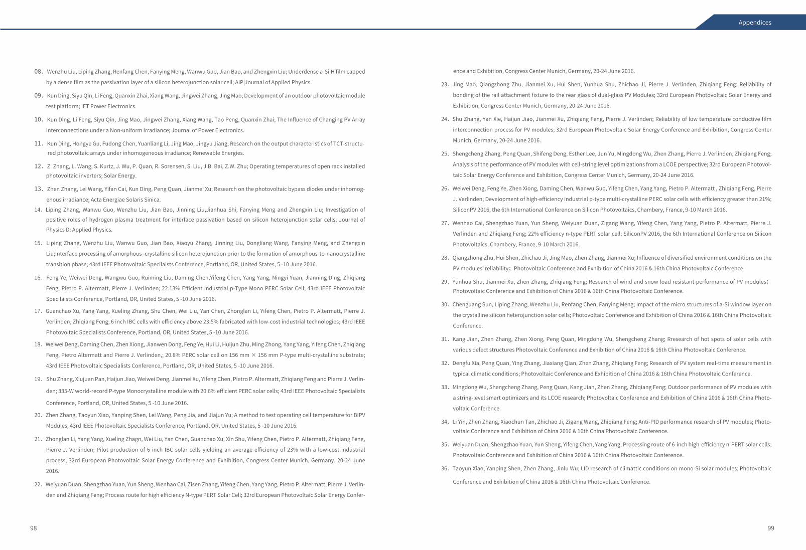
98 99
Appendices
08.Wenzhu Liu, Liping Zhang, Renfang Chen, Fanying Meng, Wanwu Guo, Jian Bao, and Zhengxin Liu; Underdense a-Si:H film capped
by a dense film as the passivation layer of a silicon heterojunction solar cell; AIP|Journal of Applied Physics.
09.Kun Ding, Siyu Qin, Li Feng, Quanxin Zhai, Xiang Wang, Jingwei Zhang, Jing Mao; Development of an outdoor photovoltaic module
test platform; IET Power Electronics.
10.Kun Ding, Li Feng, Siyu Qin, Jing Mao, Jingwei Zhang, Xiang Wang, Tao Peng, Quanxin Zhai; The Influence of Changing PV Array
Interconnections under a Non-uniform Irradiance; Journal of Power Electronics.
11.Kun Ding, Hongye Gu, Fudong Chen, Yuanliang Li, Jing Mao, Jingyu Jiang; Research on the output characteristics of TCT-structu- red photovoltaic arrays under inhomogeneous irradiance; Renewable Energies.
12.Z. Zhang, L. Wang, S. Kurtz, J. Wu, P. Quan, R. Sorensen, S. Liu, J.B. Bai, Z.W. Zhu; Operating temperatures of open rack installed photovoltaic inverters; Solar Energy.
13.Zhen Zhang, Lei Wang, Yifan Cai, Kun Ding, Peng Quan, Jianmei Xu; Research on the photovoltaic bypass diodes under inhomog-
enous irradiance; Acta Energiae Solaris Sinica.
14.Liping Zhang, Wanwu Guo, Wenzhu Liu, Jian Bao, Jinning Liu,Jianhua Shi, Fanying Meng and Zhengxin Liu; Investigation of
positive roles of hydrogen plasma treatment for interface passivation based on silicon heterojunction solar cells; Journal of
Physics D: Applied Physics.
15.Liping Zhang, Wenzhu Liu, Wanwu Guo, Jian Bao, Xiaoyu Zhang, Jinning Liu, Dongliang Wang, Fanying Meng, and Zhengxin
Liu;Interface processing of amorphous‒crystalline silicon heterojunction prior to the formation of amorphous-to-nanocrystalline
transition phase; 43rd IEEE Photovoltaic Specilaists Conference, Portland, OR, United States, 5 -10 June 2016.
16.Feng Ye, Weiwei Deng, Wangwu Guo, Ruiming Liu, Daming Chen,Yifeng Chen, Yang Yang, Ningyi Yuan, Jianning Ding, Zhiqiang
Feng, Pietro P. Altermatt, Pierre J. Verlinden; 22.13% Efficient Industrial p-Type Mono PERC Solar Cell; 43rd IEEE Photovoltaic
Specilaists Conference, Portland, OR, United States, 5 -10 June 2016.
17.Guanchao Xu, Yang Yang, Xueling Zhang, Shu Chen, Wei Liu, Yan Chen, Zhonglan Li, Yifeng Chen, Pietro P. Altermatt, Pierre J.
Verlinden, Zhiqiang Feng; 6 inch IBC cells with efficiency above 23.5% fabricated with low-cost industrial technologies; 43rd IEEE
Photovoltaic Specialists Conference, Portland, OR, United States, 5 -10 June 2016.
18.Weiwei Deng, Daming Chen, Zhen Xiong, Jianwen Dong, Feng Ye, Hui Li, Huijun Zhu, Ming Zhong, Yang Yang, Yifeng Chen, Zhiqiang
Feng, Pietro Altermatt and Pierre J. Verlinden,; 20.8% PERC solar cell on 156 mm × 156 mm P-type multi-crystalline substrate;
43rd IEEE Photovoltaic Specialists Conference, Portland, OR, United States, 5 -10 June 2016.
19.Shu Zhang, Xiujuan Pan, Haijun Jiao, Weiwei Deng, Jianmei Xu, Yifeng Chen, Pietro P. Altermatt, Zhiqiang Feng and Pierre J. Verlin-
den; 335-W world-record P-type Monocrystalline module with 20.6% efficient PERC solar cells; 43rd IEEE Photovoltaic Specialists
Conference, Portland, OR, United States, 5 -10 June 2016.
20.Zhen Zhang, Taoyun Xiao, Yanping Shen, Lei Wang, Peng Jia, and Jiajun Yu; A method to test operating cell temperature for BIPV
Modules; 43rd IEEE Photovoltaic Specialists Conference, Portland, OR, United States, 5 -10 June 2016.
21.Zhonglan Li, Yang Yang, Xueling Zhagn, Wei Liu, Yan Chen, Guanchao Xu, Xin Shu, Yifeng Chen, Pietro P. Altermatt, Zhiqiang Feng,
Pierre J. Verlinden; Pilot production of 6 inch IBC solar cells yielding an average efficiency of 23% with a low-cost industrial
process; 32rd European Photovoltaic Solar Energy Conference and Exhibition, Congress Center Munich, Germany, 20-24 June
2016.
22.Weiyuan Duan, Shengzhao Yuan, Yun Sheng, Wenhao Cai, Zisen Zhang, Yifeng Chen, Yang Yang, Pietro P. Altermatt, Pierre J. Verlin-
den and Zhiqiang Feng; Process route for high efficiency N-type PERT Solar Cell; 32rd European Photovoltaic Solar Energy Confer-
ence and Exhibition, Congress Center Munich, Germany, 20-24 June 2016.
23.Jing Mao, Qiangzhong Zhu, Jianmei Xu, Hui Shen, Yunhua Shu, Zhichao Ji, Pierre J. Verlinden, Zhiqiang Feng; Reliability of
bonding of the rail attachment fixture to the rear glass of dual-glass PV Modules; 32rd European Photovoltaic Solar Energy and
Exhibition, Congress Center Munich, Germany, 20-24 June 2016.
24.Shu Zhang, Yan Xie, Haijun Jiao, Jianmei Xu, Zhiqiang Feng, Pierre J. Verlinden; Reliability of low temperature conductive film
interconnection process for PV modules; 32rd European Photovoltaic Solar Energy Conference and Exhibition, Congress Center
Munich, Germany, 20-24 June 2016.
25.Shengcheng Zhang, Peng Quan, Shifeng Deng, Esther Lee, Jun Yu, Mingdong Wu, Zhen Zhang, Pierre J. Verlinden, Zhiqiang Feng;
Analysis of the performance of PV modules with cell-string level optimizations from a LCOE perspective; 32rd European Photovol-
taic Solar Energy Conference and Exhibition, Congress Center Munich, Germany, 20-24 June 2016.
26.Weiwei Deng, Feng Ye, Zhen Xiong, Daming Chen, Wanwu Guo, Yifeng Chen, Yang Yang, Pietro P. Altermatt , Zhiqiang Feng, Pierre
J. Verlinden; Development of high-efficiency industrial p-type multi-crystalline PERC solar cells with efficiency greater than 21%;
SiliconPV 2016, the 6th International Conference on Silicon Photovoltaics, Chambery, France, 9-10 March 2016.
27.Wenhao Cai, Shengzhao Yuan, Yun Sheng, Weiyuan Duan, Zigang Wang, Yifeng Chen, Yang Yang, Pietro P. Altermatt, Pierre J.
Verlinden and Zhiqiang Feng; 22% efficiency n-type PERT solar cell; SiliconPV 2016, the 6th International Conference on Silicon
Photovoltaics, Chambery, France, 9-10 March 2016.
28.Qiangzhong Zhu, Hui Shen, Zhichao Ji, Jing Mao, Zhen Zhang, Jianmei Xu; Influence of diversified environment conditions on the
PV modules' reliability;Photovoltaic Conference and Exhibition of China 2016 & 16th China Photovoltaic Conference.
29.Yunhua Shu, Jianmei Xu, Zhen Zhang, Zhiqiang Feng; Research of wind and snow load resistant performance of PV modules;Photovoltaic Conference and Exhibition of China 2016 & 16th China Photovoltaic Conference.
30.Chenguang Sun, Liping Zhang, Wenzhu Liu, Renfang Chen, Fanying Meng; Impact of the micro structures of a-Si window layer on
the crystalline silicon heterojunction solar cells; Photovoltaic Conference and Exhibition of China 2016 & 16th China Photovoltaic
Conference.
31.Kang Jian, Zhen Zhang, Zhen Xiong, Peng Quan, Mingdong Wu, Shengcheng Zhang; Rresearch of hot spots of solar cells with
various defect structures Photovoltaic Conference and Exhibition of China 2016 & 16th China Photovoltaic Conference.
32.Dengfu Xia, Peng Quan, Ying Zhang, Jiaxiang Qian, Zhen Zhang, Zhiqiang Feng; Research of PV system real-time measurement in
typical climatic conditions; Photovoltaic Conference and Exhibition of China 2016 & 16th China Photovoltaic Conference.
33.Mingdong Wu, Shengcheng Zhang, Peng Quan, Kang Jian, Zhen Zhang, Zhiqiang Feng; Outdoor performance of PV modules with
a string-level smart optimizers and its LCOE research; Photovoltaic Conference and Exhibition of China 2016 & 16th China Photo-
voltaic Conference.
34.Li Yin, Zhen Zhang, Xiaochun Tan, Zhichao Ji, Zigang Wang, Zhiqiang Feng; Anti-PID performance research of PV modules; Photo-voltaic Conference and Exhibition of China 2016 & 16th China Photovoltaic Conference.
35.Weiyuan Duan, Shengzhao Yuan, Yun Sheng, Yifeng Chen, Yang Yang; Processing route of 6-inch high-efficiency n-PERT solar cells;
Photovoltaic Conference and Exhibition of China 2016 & 16th China Photovoltaic Conference.
36.Taoyun Xiao, Yanping Shen, Zhen Zhang, Jinlu Wu; LID research of climattic conditions on mono-Si solar modules; Photovoltaic
Conference and Exhibition of China 2016 & 16th China Photovoltaic Conference.