Embed Size (px)
Citation preview

Julia Thom 1
Sensor R&D at Cornell, SiD
Argonne SiD Workshop, 6/4/2010Julia Thom,Cornell University
Cornell UniversityFloyd R. Newman Laboratory forElementary-Particle Physics
Julia Thom 2
Investigating new techniques fornovel HEP pixel detectors
• Trend towards miniaturization and complex circuits on thinsensors– monolithic detectors (e.g.MAPS), 3D integrated circuits, …
• Applications of 3D technology to future HEP detectors: S-LHC, ILC
– Emerging “vertically integrated” (3D) devices with SOI technology– Attractive due to low power, high resolution, high S/N, short
integration time, low material budget, radiation hardness, “edgeless”design,..
– Ongoing R&D program at FNAL to define options for ILC application
Julia Thom 3
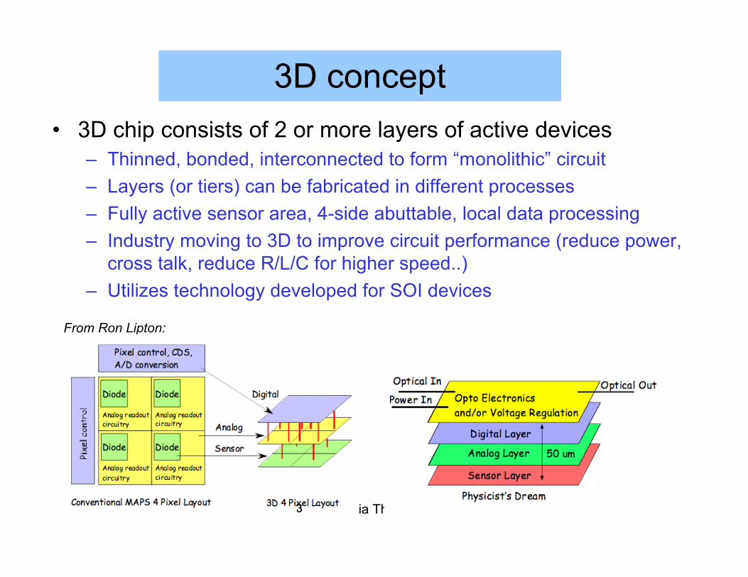
3D concept• 3D chip consists of 2 or more layers of active devices
– Thinned, bonded, interconnected to form “monolithic” circuit– Layers (or tiers) can be fabricated in different processes– Fully active sensor area, 4-side abuttable, local data processing– Industry moving to 3D to improve circuit performance (reduce power,
cross talk, reduce R/L/C for higher speed..)– Utilizes technology developed for SOI devices
From Ron Lipton:

Julia Thom 4
Silicon on Insulator
• Silicon on Insulator:– Thin active circuit layer on
insulating substrate.• 200nm of silicon on buried oxide
(BOX), carried on handle wafer– handle wafer can be high grade
silicon- combine electronics andfully depleted detector in singlewafer
– Diode can be formed byimplantation through the BOX
– SOI wafer integrated into 3Dconcept

Julia Thom 5
Key Technologies for SOI/3D
From R.Lipton
Julia Thom 6
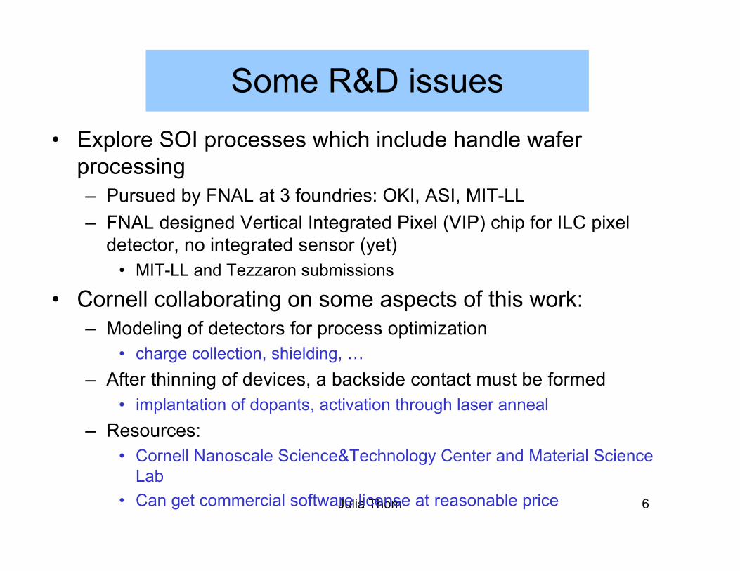
Some R&D issues• Explore SOI processes which include handle wafer
processing– Pursued by FNAL at 3 foundries: OKI, ASI, MIT-LL– FNAL designed Vertical Integrated Pixel (VIP) chip for ILC pixel
detector, no integrated sensor (yet)• MIT-LL and Tezzaron submissions
• Cornell collaborating on some aspects of this work:– Modeling of detectors for process optimization
• charge collection, shielding, …– After thinning of devices, a backside contact must be formed
• implantation of dopants, activation through laser anneal– Resources:
• Cornell Nanoscale Science&Technology Center and Material ScienceLab
• Can get commercial software license at reasonable price
7
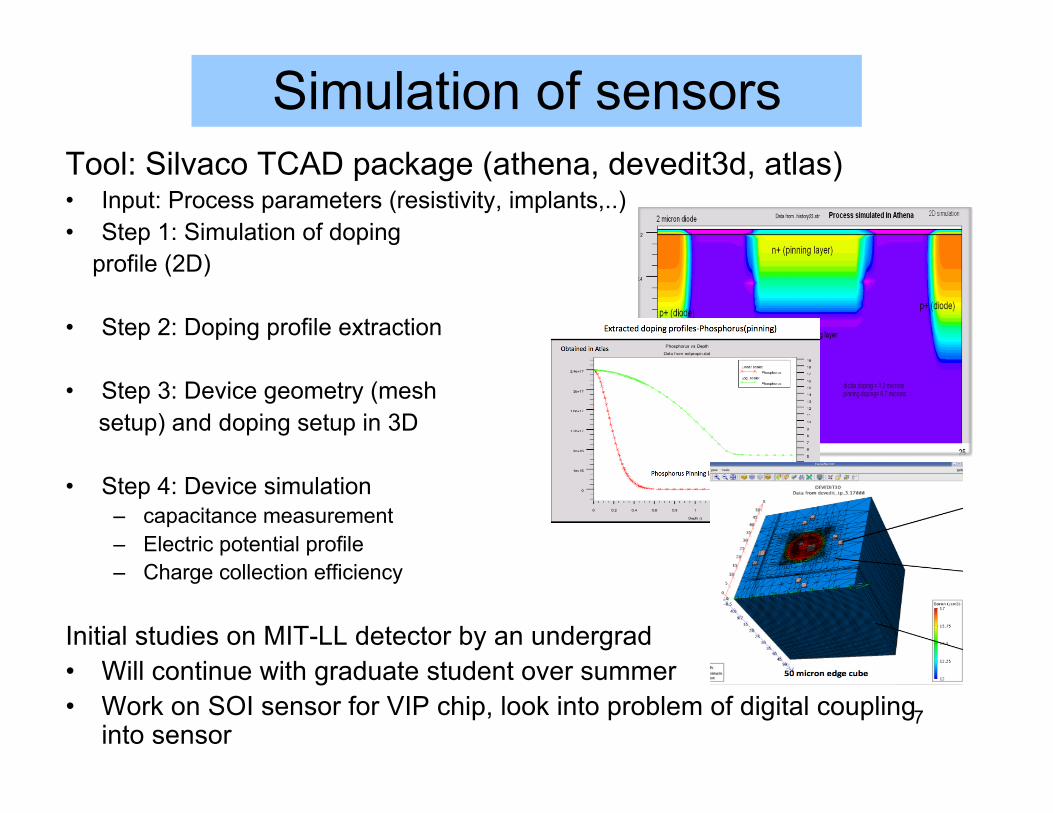
Simulation of sensorsTool: Silvaco TCAD package (athena, devedit3d, atlas)• Input: Process parameters (resistivity, implants,..)• Step 1: Simulation of doping profile (2D)
• Step 2: Doping profile extraction
• Step 3: Device geometry (mesh setup) and doping setup in 3D
• Step 4: Device simulation– capacitance measurement– Electric potential profile– Charge collection efficiency
Initial studies on MIT-LL detector by an undergrad• Will continue with graduate student over summer• Work on SOI sensor for VIP chip, look into problem of digital coupling
into sensor

8
Simulation of sensors
• Use to study sensor features like pinned diodes, edgetrenches, channel stops etc.– charge collection efficiency?– optimal spacing of diodes?
• Example: “edgeless” pixel detector MIT-LL
electron passing through detector
Julia Thom 9
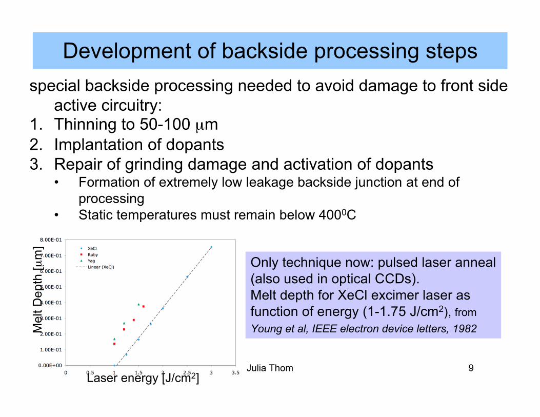
special backside processing needed to avoid damage to front sideactive circuitry:
1. Thinning to 50-100 µm2. Implantation of dopants3. Repair of grinding damage and activation of dopants
• Formation of extremely low leakage backside junction at end ofprocessing
• Static temperatures must remain below 4000C
Development of backside processing steps
Only technique now: pulsed laser anneal(also used in optical CCDs).Melt depth for XeCl excimer laser as function of energy (1-1.75 J/cm2), fromYoung et al, IEEE electron device letters, 1982
Laser energy [J/cm2]
Mel
t Dep
th [µ
m]
Julia Thom 10Beam spot 1x1 cm,uniform exposure, XeCl laser(308nm; 30ns)
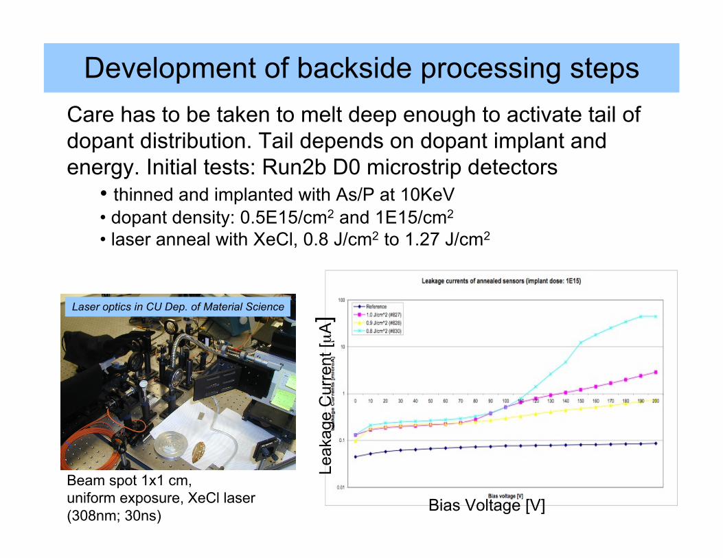
Care has to be taken to melt deep enough to activate tail ofdopant distribution. Tail depends on dopant implant andenergy. Initial tests: Run2b D0 microstrip detectors
• thinned and implanted with As/P at 10KeV• dopant density: 0.5E15/cm2 and 1E15/cm2
• laser anneal with XeCl, 0.8 J/cm2 to 1.27 J/cm2
Development of backside processing steps
Laser optics in CU Dep. of Material Science
Bias Voltage [V]
Leak
age
Cur
rent
[µA]
11
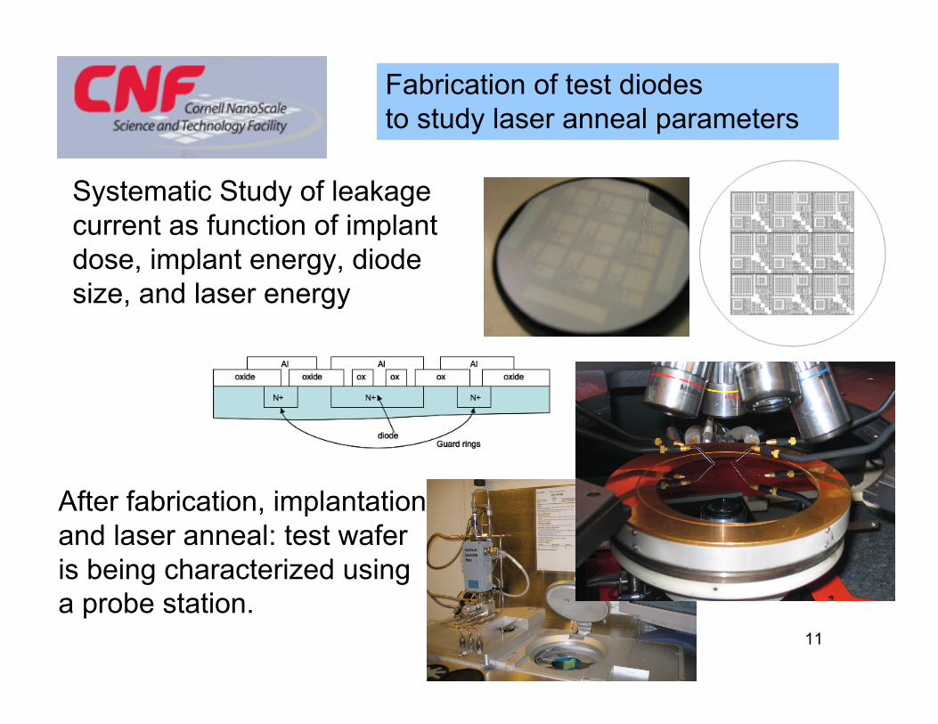
Systematic Study of leakagecurrent as function of implantdose, implant energy, diodesize, and laser energy
Fabrication of test diodesto study laser anneal parameters
After fabrication, implantation and laser anneal: test wafer is being characterized using a probe station.
12
SummaryHave been exploring issues related to 3D/SOI
devices at Cornell• Simulations of FNAL design SOI processes
– Goal: provide feedback to ILC sensor design fordemonstration of 3D technology over summer
– Will start to work on SOI sensor from OKI/KEK• laser annealing of thinned SOI-based sensors
– Have developed process to implant and anneal thinsensors at Cornell
– In process of working on SOI devices from OKI– May also be useful for DEPFET sensors

Julia Thom 13
backup
Julia Thom 14
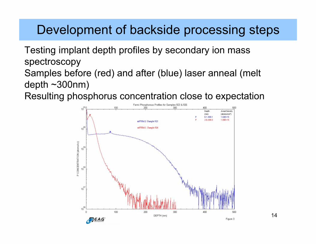
Testing implant depth profiles by secondary ion massspectroscopySamples before (red) and after (blue) laser anneal (meltdepth ~300nm)Resulting phosphorus concentration close to expectation
Development of backside processing steps