Embed Size (px)
Citation preview
CLICdp-Note-2016-00409 June 2016
TCAD simulations of High-Voltage-CMOS Pixel structuresfor the CLIC vertex detector
M. Buckland1)⇤†
⇤ University of Liverpool, England, † CERN, Switzerland
Abstract
The requirements for precision physics and the experimental conditions at CLIC result instringent constraints for the vertex detector. Capacitively coupled active pixel sensors with25 µm pitch implemented in a commercial 180 nm High-Voltage CMOS (HV-CMOS) pro-cess are currently under study as a candidate technology for the CLIC vertex detector. Labor-atory calibration measurements and beam tests with prototypes are complemented by de-tailed TCAD and electronic circuit simulations, aiming for a comprehensive understandingof the signal formation in the HV-CMOS sensors and subsequent readout stages. In this note2D and 3D TCAD simulation results of the prototype sensor, the Capacitively Coupled PixelDetector version three (CCPDv3), will be presented. These include the electric field distri-bution, leakage current, well capacitance, transient response to minimum ionising particlesand charge-collection.
This work was carried out in the framework of the CLICdp collaboration
2 Capacitively coupled pixel detector
1 Introduction
The Compact Linear Collider (CLIC) is a proposed electron-positron collider to be constructed in threeenergy stages [1]. The final stage has a maximum centre-of-mass energy of 3 TeV. The CLIC vertexdetector has to perform precision physics measurements in a challenging environment, with high ratesof beam-induced background particles. The principal requirements for the detector are: a single hitresolution of 3 µm, very low mass (⇡ 0.2% X0 per layer), very low power dissipation (compatible withair-flow cooling) and pulsed power operation, complemented with 10 ns time stamping capabilities.
Current solutions for vertex detectors are not sufficient to reach these goals. They use hybrid pixeldetectors, which consist of a segmented silicon sensor connected to a segmented readout chip via bumpbonding. An alternate way to do this is by capacitively coupling the two. This has the benefit of beingmuch more cost effective as well as reducing material budget. To insure good signal transfer the signalneeds to be large, this is typically achieved by each pixel containing an amplifier. One candidate sensortechnology is an active High-Voltage CMOS sensor (HV-CMOS), in which a high-field drift zone and acharge-sensitive amplifier are integrated in the same device.
By performing simulations of the proposed sensors, a better understanding of the features of the meas-urements such as transient signal development is achieved. Technology Computer Aided Design (TCAD)is a powerful tool for simulating and optimising semiconductor fabrication processes and device opera-tion [2]. In order to model the structural properties and electrical behaviour of semiconductor devicesTCAD uses the finite element method. This technique is used to find approximate solutions to the phys-ical partial differential equations, such as the continuity and diffusion equations. For this study SynopsysTCAD version I-2013.12 was used.
To improve the comparison between the measurements and simulation an accurate model of the sensorwas created. In this note details of the TCAD simulation method as well as results from the simulation arepresented. One model is a 3-dimensional structure of a single-pixel that is used to validate a simplified2-dimensional single pixel model. Another is a three-pixel structure based on the validated 2D-model.
2 Capacitively coupled pixel detector
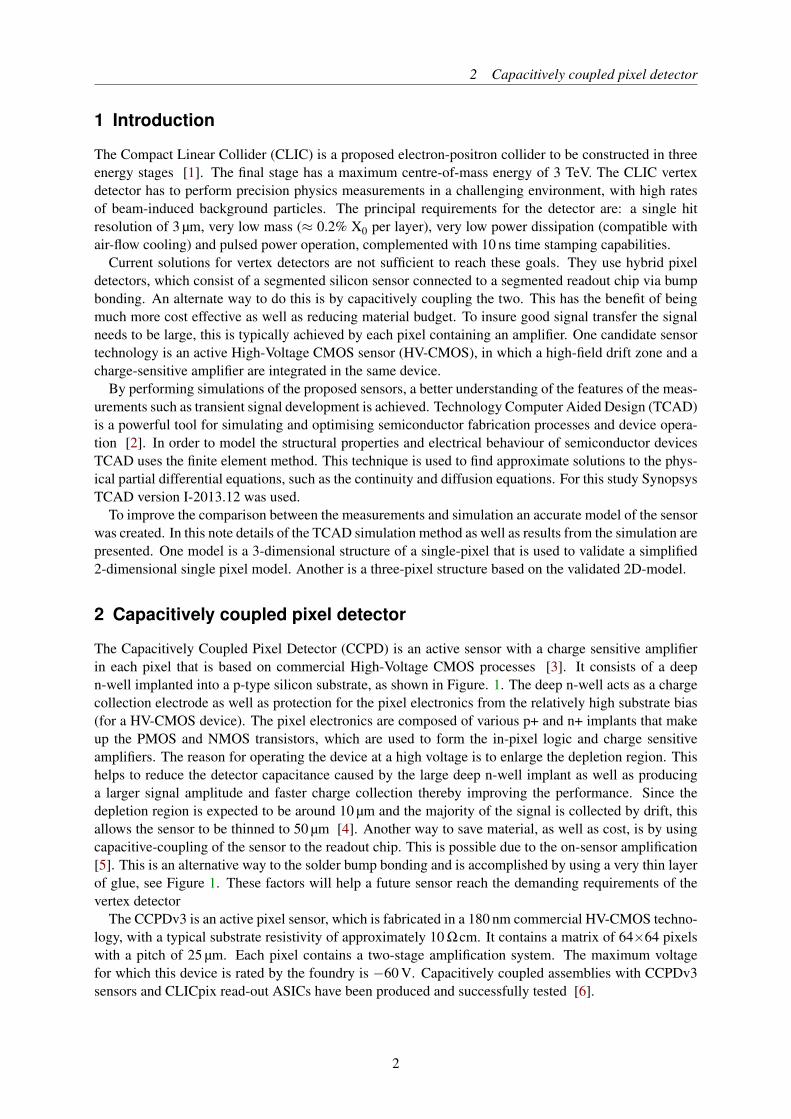
The Capacitively Coupled Pixel Detector (CCPD) is an active sensor with a charge sensitive amplifierin each pixel that is based on commercial High-Voltage CMOS processes [3]. It consists of a deepn-well implanted into a p-type silicon substrate, as shown in Figure. 1. The deep n-well acts as a chargecollection electrode as well as protection for the pixel electronics from the relatively high substrate bias(for a HV-CMOS device). The pixel electronics are composed of various p+ and n+ implants that makeup the PMOS and NMOS transistors, which are used to form the in-pixel logic and charge sensitiveamplifiers. The reason for operating the device at a high voltage is to enlarge the depletion region. Thishelps to reduce the detector capacitance caused by the large deep n-well implant as well as producinga larger signal amplitude and faster charge collection thereby improving the performance. Since thedepletion region is expected to be around 10 µm and the majority of the signal is collected by drift, thisallows the sensor to be thinned to 50 µm [4]. Another way to save material, as well as cost, is by usingcapacitive-coupling of the sensor to the readout chip. This is possible due to the on-sensor amplification[5]. This is an alternative way to the solder bump bonding and is accomplished by using a very thin layerof glue, see Figure 1. These factors will help a future sensor reach the demanding requirements of thevertex detector
The CCPDv3 is an active pixel sensor, which is fabricated in a 180 nm commercial HV-CMOS techno-logy, with a typical substrate resistivity of approximately 10 Wcm. It contains a matrix of 64⇥64 pixelswith a pitch of 25 µm. Each pixel contains a two-stage amplification system. The maximum voltagefor which this device is rated by the foundry is �60 V. Capacitively coupled assemblies with CCPDv3sensors and CLICpix read-out ASICs have been produced and successfully tested [6].
2
3 Comparison of 2D and 3D models
Figure 1: Schematic of the CCPDv3 detector coupled to the CLICpix readout chip via a thin glue layer.
3 Comparison of 2D and 3D models
A comparison between a 2D model and a 3D model has been carried out to establish the validity of the2D simulations. The reason for this is that the 3D simulations are very memory intensive using largeamounts of RAM and as a result take a long time to simulate. Due to this there is a trade off between themesh size, and hence convergence of the model, with the memory usage. Therefore the 2D simulationsare much quicker in comparison.
3.1 Simulated structures
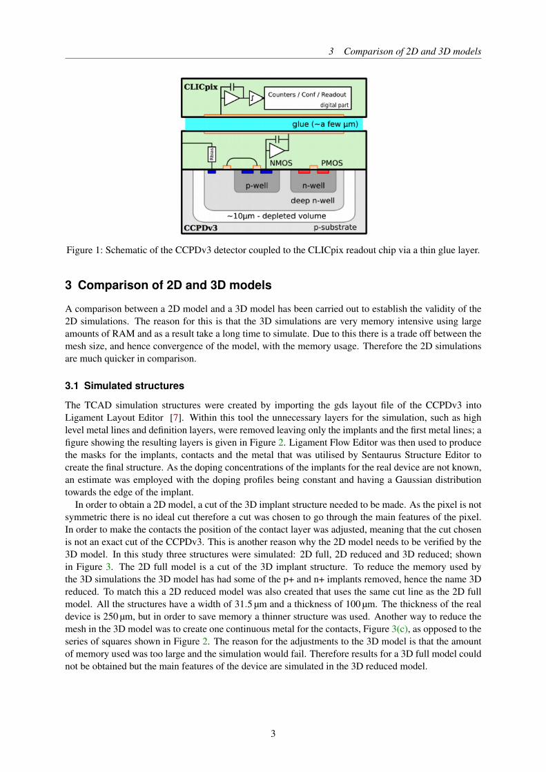
The TCAD simulation structures were created by importing the gds layout file of the CCPDv3 intoLigament Layout Editor [7]. Within this tool the unnecessary layers for the simulation, such as highlevel metal lines and definition layers, were removed leaving only the implants and the first metal lines; afigure showing the resulting layers is given in Figure 2. Ligament Flow Editor was then used to producethe masks for the implants, contacts and the metal that was utilised by Sentaurus Structure Editor tocreate the final structure. As the doping concentrations of the implants for the real device are not known,an estimate was employed with the doping profiles being constant and having a Gaussian distributiontowards the edge of the implant.
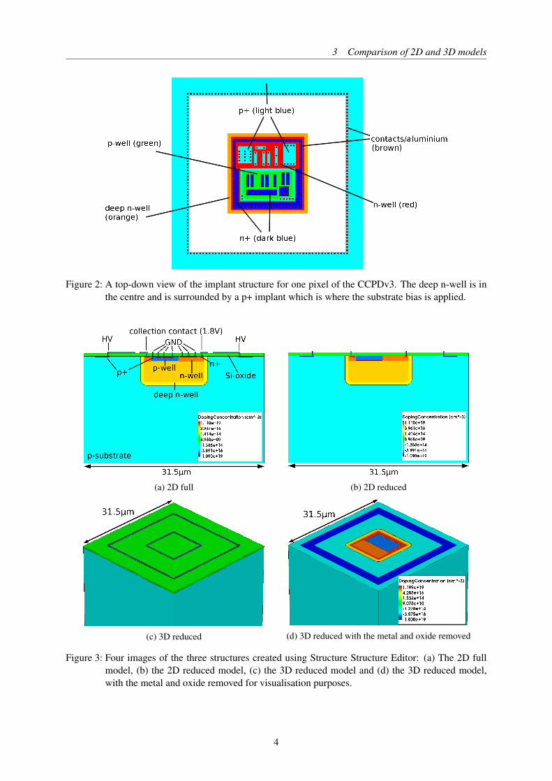
In order to obtain a 2D model, a cut of the 3D implant structure needed to be made. As the pixel is notsymmetric there is no ideal cut therefore a cut was chosen to go through the main features of the pixel.In order to make the contacts the position of the contact layer was adjusted, meaning that the cut chosenis not an exact cut of the CCPDv3. This is another reason why the 2D model needs to be verified by the3D model. In this study three structures were simulated: 2D full, 2D reduced and 3D reduced; shownin Figure 3. The 2D full model is a cut of the 3D implant structure. To reduce the memory used bythe 3D simulations the 3D model has had some of the p+ and n+ implants removed, hence the name 3Dreduced. To match this a 2D reduced model was also created that uses the same cut line as the 2D fullmodel. All the structures have a width of 31.5 µm and a thickness of 100 µm. The thickness of the realdevice is 250 µm, but in order to save memory a thinner structure was used. Another way to reduce themesh in the 3D model was to create one continuous metal for the contacts, Figure 3(c), as opposed to theseries of squares shown in Figure 2. The reason for the adjustments to the 3D model is that the amountof memory used was too large and the simulation would fail. Therefore results for a 3D full model couldnot be obtained but the main features of the device are simulated in the 3D reduced model.
3
3 Comparison of 2D and 3D models
Figure 2: A top-down view of the implant structure for one pixel of the CCPDv3. The deep n-well is inthe centre and is surrounded by a p+ implant which is where the substrate bias is applied.
(a) 2D full (b) 2D reduced
(c) 3D reduced (d) 3D reduced with the metal and oxide removed
Figure 3: Four images of the three structures created using Structure Structure Editor: (a) The 2D fullmodel, (b) the 2D reduced model, (c) the 3D reduced model and (d) the 3D reduced model,with the metal and oxide removed for visualisation purposes.
4

3 Comparison of 2D and 3D models
In addition to defining the geometry and doping profiles of the structure, a mesh is also defined. Themesh of the three models are all created using the same methods. However, in order to reduce thememory size in the 3D model a larger mesh size was applied than for the 2D models. A global meshthat refines around the doping concentration within the silicon bulk is first defined. This helps to ensurethat the doping profiles of the implants are adequately resolved avoiding inaccurate results. The chosenrefinement function is f (x) = arsinh(x) and checks whether the function value difference between twomesh points is above a certain value and then meshes accordingly. To aid with the electrical simulationsof the model two refinement windows are placed in addition to the global mesh. One was set so that afiner mesh was around the depletion region, and the other was placed along the path of the particle forthe corresponding simulation created.
3.2 Simulation results
The electrical properties and device performance of the CCPDv3 structures are simulated using SentaurusDevice. This is a tool that is used to simulate the electrical, thermal and optical characteristics of siliconbased semiconductor devices.
3.2.1 Electric Field
(a) 2D full (b) 2D reduced
(c) 3D reduced (d) 2D cut of 3D reduced
Figure 4: Absolute value of the electric field at an applied bias of �60 V: (a) the 2D full model, (b) the2D reduced model, (c) the 3D reduced model and (d) a cut through the centre of the 3D reducedmodel.
5
3 Comparison of 2D and 3D models
To acquire the absolute value of the electric field all three models were biased to �60 V, the typicaloperating voltage of the device. In all three structures the electric field showed the same trends (shownin Figure 4) of high field inside the depletion region and low fields outside the depletion region, as wellas inside the deep n-well. The highest field region is found at the corners of the deep n-well. In the3D reduced model the high field also exists at the diagonal corners of the deep n-well implant near thesurface, a feature that cannot be replicated in the 2D models. The exception to this is that in the 2D fullmodel the high field extends up to and inside the oxide which can be attributed to the extended metallines. Since the size of the mesh determines the resolution of the extracted values, a larger mesh meanssmaller resolution. Due to this the electric field map in the 2D cut of the 3D reduced model is not assmooth as the 2D reduced electric field map.
3.2.2 Leakage current and capacitance
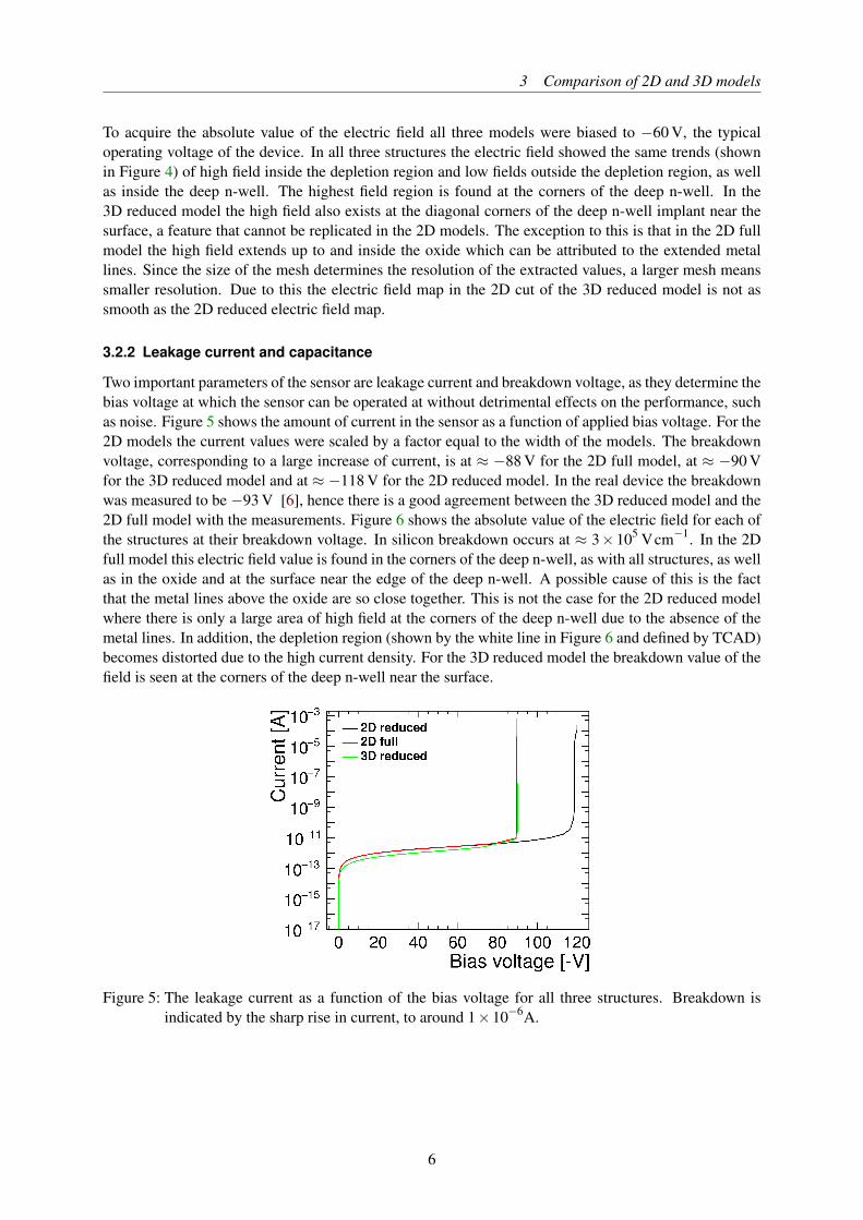
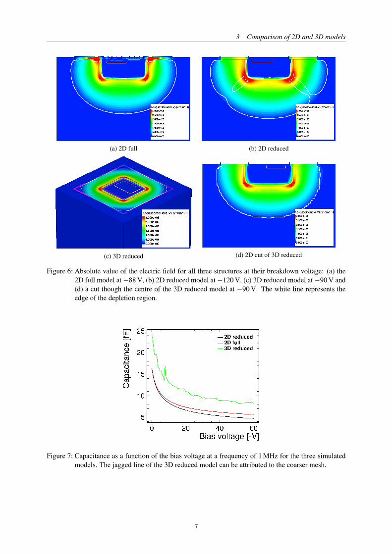
Two important parameters of the sensor are leakage current and breakdown voltage, as they determine thebias voltage at which the sensor can be operated at without detrimental effects on the performance, suchas noise. Figure 5 shows the amount of current in the sensor as a function of applied bias voltage. For the2D models the current values were scaled by a factor equal to the width of the models. The breakdownvoltage, corresponding to a large increase of current, is at ⇡ �88 V for the 2D full model, at ⇡ �90 Vfor the 3D reduced model and at ⇡ �118 V for the 2D reduced model. In the real device the breakdownwas measured to be �93 V [6], hence there is a good agreement between the 3D reduced model and the2D full model with the measurements. Figure 6 shows the absolute value of the electric field for each ofthe structures at their breakdown voltage. In silicon breakdown occurs at ⇡ 3⇥105 Vcm�1. In the 2Dfull model this electric field value is found in the corners of the deep n-well, as with all structures, as wellas in the oxide and at the surface near the edge of the deep n-well. A possible cause of this is the factthat the metal lines above the oxide are so close together. This is not the case for the 2D reduced modelwhere there is only a large area of high field at the corners of the deep n-well due to the absence of themetal lines. In addition, the depletion region (shown by the white line in Figure 6 and defined by TCAD)becomes distorted due to the high current density. For the 3D reduced model the breakdown value of thefield is seen at the corners of the deep n-well near the surface.
Figure 5: The leakage current as a function of the bias voltage for all three structures. Breakdown isindicated by the sharp rise in current, to around 1⇥10�6A.
6
3 Comparison of 2D and 3D models
(a) 2D full (b) 2D reduced
(c) 3D reduced (d) 2D cut of 3D reduced
Figure 6: Absolute value of the electric field for all three structures at their breakdown voltage: (a) the2D full model at �88 V, (b) 2D reduced model at �120 V, (c) 3D reduced model at �90 V and(d) a cut though the centre of the 3D reduced model at �90 V. The white line represents theedge of the depletion region.
Figure 7: Capacitance as a function of the bias voltage at a frequency of 1 MHz for the three simulatedmodels. The jagged line of the 3D reduced model can be attributed to the coarser mesh.
7

3 Comparison of 2D and 3D models
The deep n-well-to-bulk capacitance value was simulated using small signal AC analysis and themixed mode of Sentaurus Device at a frequency of 1 MHz. It measures current changes in the circuit inresponse to a small perturbation of the voltage at a contact node. The capacitance is then determined bymeasuring the out-of-phase response of the current with the voltage. Test bench calculations estimatedthis value to be ⇠10 fF at �60 V. The results of the simulation shown in Figure 7 are consistent with thecalculations. At �60 V the 2D models have similar values at around 5 fF while the 3D reduced modelhas a higher value of 8 fF. The 3D reduced model response is jagged due to the coarser mesh. The valuesobtained from the 2D models are obtained in the units of Fµm�1 and are then multiplied by the length ofthe deep n-well to produce the final value. For this reason they can only be considered as estimates.
3.2.3 Response to Minimum Ionising Particle
To simulate a Minimum Ionising Particle (MIP) in TCAD the Heavy Ion Model of Sentaurus Device isused with the time, direction, position and charge deposition of the particle specified in the commandfile. The temporal and spatial deposition of charge are modelled with Gaussian distributions. The widthof the temporal Gaussian is 2 ps. Due to this, the time at which the MIP enters the transient simulationis not 0 s but 10 ps so that the signal does not become distorted and the current is allowed to settle. Thewidth of the spatial distribution is defined in the command file and was 0.035 µm. In this study the MIPpasses through the centre of all three structures and deposits 80 electron-hole pairs per µm over a depthof 100 µm, with no landau fluctuations taken into account.
A transient simulation from 0–10 µs was performed at a bias voltage of �60 V, and the current obtainedat the collection contacts was measured (each contact is Ohmic and has a resistance value of 1 mW). Thepulse shape in the first 0.5 ns is shown in Figure 8. The 3D reduced model has the largest and fastestpeak but quickly drops to the lowest value. At all times the 2D full model has a larger current value thanthe 2D reduced model due to the metal lines and extra implants.
Figure 8: The current induced on the collection contact when a MIP passes through the centre of thepixel cell.
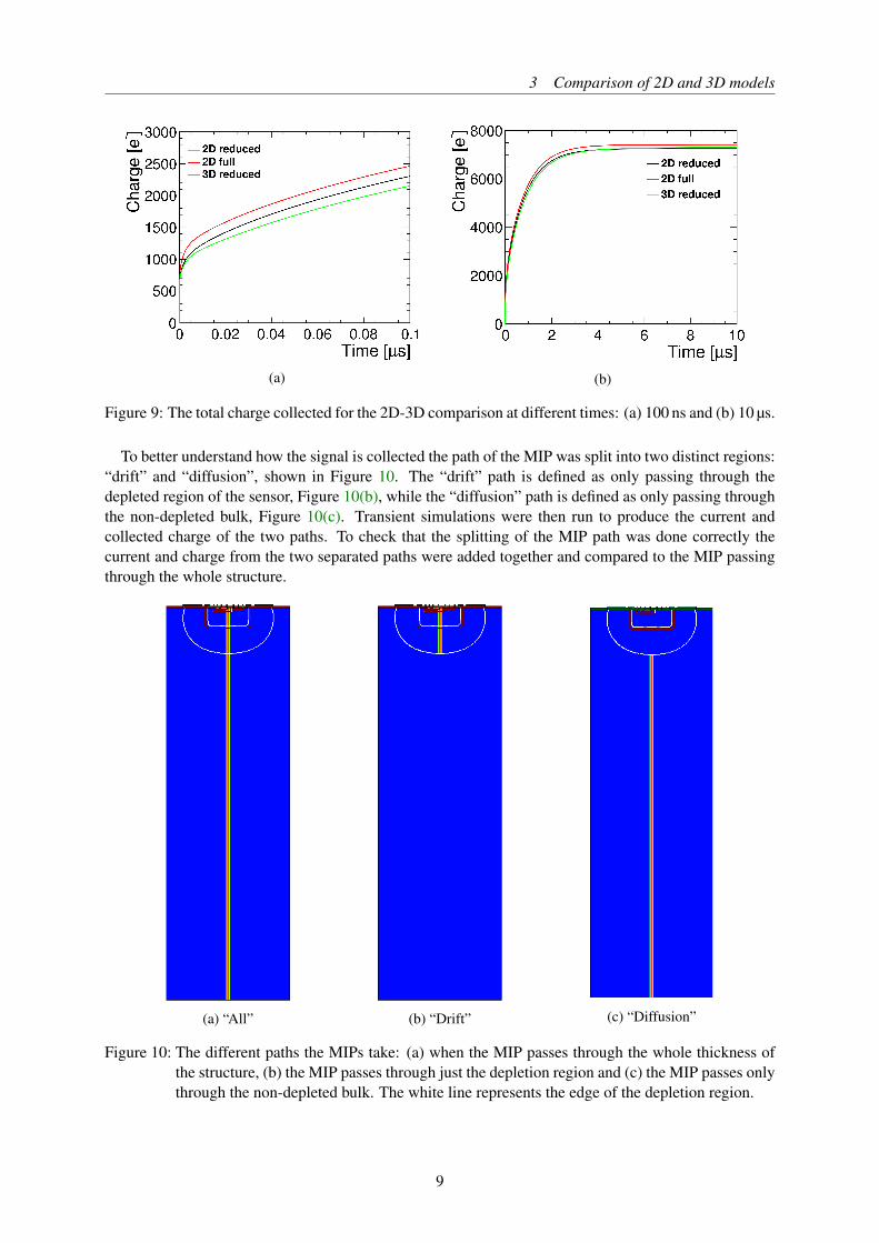
The collected charge is found by integrating the current over time, see Figure 9. After 100 ns thedifference between all three models is around 300 e� with 3D reduced collecting the least and 2D fullcollecting the most. However after 10 µs the difference between all three models reduces slightly toaround 200 e�, which amounts to a difference of ⇡ 3%. Also, after 10 µs the 2D reduced model collectsthe least amount of charge; this change in order occurs at around 4 µs.
Based on all the result of the 2D-3D comparison the 2D full model is a good approximation of the 3Dmodel and will be used for the three-pixel structure described in Section 4.
8
3 Comparison of 2D and 3D models
(a) (b)
Figure 9: The total charge collected for the 2D-3D comparison at different times: (a) 100 ns and (b) 10 µs.
To better understand how the signal is collected the path of the MIP was split into two distinct regions:“drift” and “diffusion”, shown in Figure 10. The “drift” path is defined as only passing through thedepleted region of the sensor, Figure 10(b), while the “diffusion” path is defined as only passing throughthe non-depleted bulk, Figure 10(c). Transient simulations were then run to produce the current andcollected charge of the two paths. To check that the splitting of the MIP path was done correctly thecurrent and charge from the two separated paths were added together and compared to the MIP passingthrough the whole structure.
(a) “All” (b) “Drift” (c) “Diffusion”
Figure 10: The different paths the MIPs take: (a) when the MIP passes through the whole thickness ofthe structure, (b) the MIP passes through just the depletion region and (c) the MIP passes onlythrough the non-depleted bulk. The white line represents the edge of the depletion region.
9
3 Comparison of 2D and 3D models
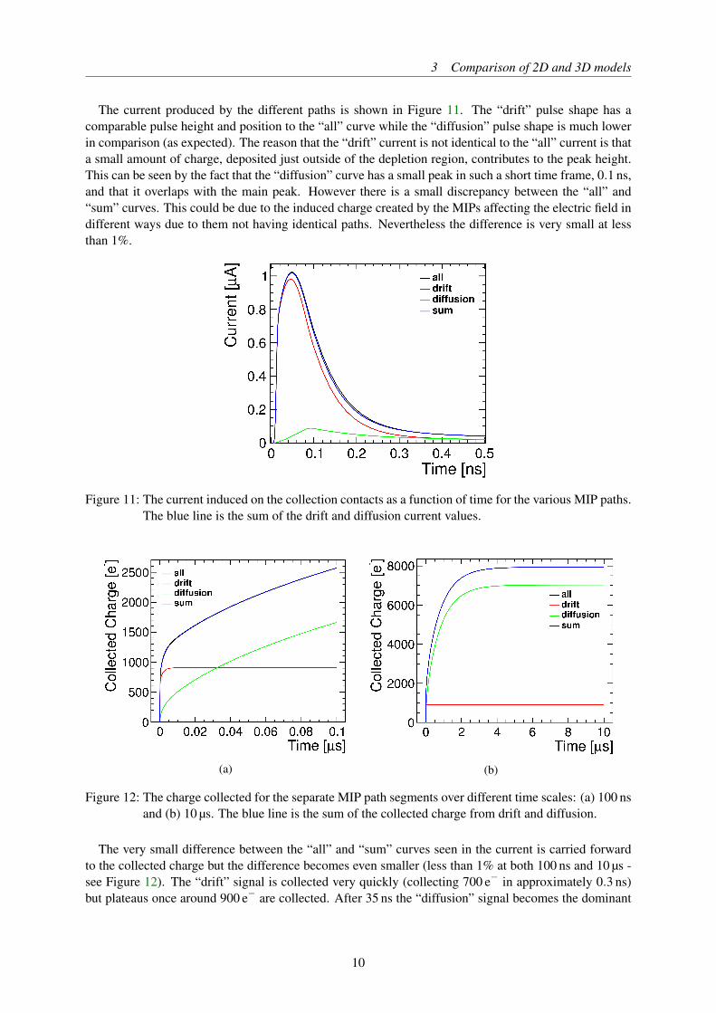
The current produced by the different paths is shown in Figure 11. The “drift” pulse shape has acomparable pulse height and position to the “all” curve while the “diffusion” pulse shape is much lowerin comparison (as expected). The reason that the “drift” current is not identical to the “all” current is thata small amount of charge, deposited just outside of the depletion region, contributes to the peak height.This can be seen by the fact that the “diffusion” curve has a small peak in such a short time frame, 0.1 ns,and that it overlaps with the main peak. However there is a small discrepancy between the “all” and“sum” curves. This could be due to the induced charge created by the MIPs affecting the electric field indifferent ways due to them not having identical paths. Nevertheless the difference is very small at lessthan 1%.
Figure 11: The current induced on the collection contacts as a function of time for the various MIP paths.The blue line is the sum of the drift and diffusion current values.
(a) (b)
Figure 12: The charge collected for the separate MIP path segments over different time scales: (a) 100 nsand (b) 10 µs. The blue line is the sum of the collected charge from drift and diffusion.
The very small difference between the “all” and “sum” curves seen in the current is carried forwardto the collected charge but the difference becomes even smaller (less than 1% at both 100 ns and 10 µs -see Figure 12). The “drift” signal is collected very quickly (collecting 700 e� in approximately 0.3 ns)but plateaus once around 900 e� are collected. After 35 ns the “diffusion” signal becomes the dominant
10
4 Three-pixel structure
method of charge collection and after 10 µs contributes to around 88% of the total charge collected. Thevalue of 88% should be considered as specific to the simulated structure. This is because it is onlya single pixel so there is no diffusion to neighbours and the fractional contribution from diffusion alsodepends on thickness. For the real sensor, with a thickness of 250 µm, the amount of “drift” charge wouldstay the same but there would be a larger contribution from the “diffusion” part. A way to increase theamount of fast (drift) signal would be to create a larger depletion region which can be done in two ways:by an increase in the bias voltage or an increase in the bulk resistivity. As this sensor technology is beingoperated at the maximum bias voltage this only leaves the option to increase bulk resistivity.
4 Three-pixel structure
As shown in the previous section, the 2D full model is a good approximation of the memory intensive3D model. In this section the simulation method and results of the 2D full model are extended to includea three-pixel structure. The reason to create a three-pixel structure is to look at charge-sharing betweenneighbouring pixels and to investigate the variation of the collected charge for different MIP positionsacross the pixel unit cell.
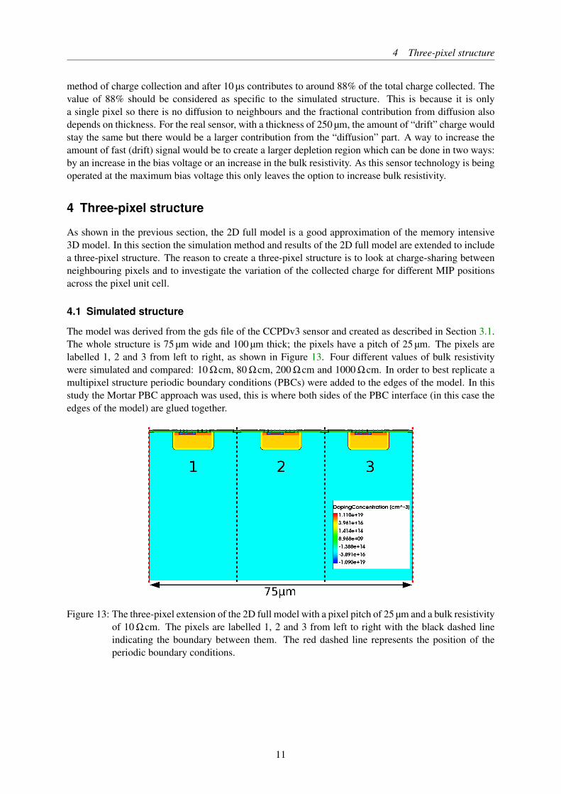
4.1 Simulated structure
The model was derived from the gds file of the CCPDv3 sensor and created as described in Section 3.1.The whole structure is 75 µm wide and 100 µm thick; the pixels have a pitch of 25 µm. The pixels arelabelled 1, 2 and 3 from left to right, as shown in Figure 13. Four different values of bulk resistivitywere simulated and compared: 10 Wcm, 80 Wcm, 200 Wcm and 1000 Wcm. In order to best replicate amultipixel structure periodic boundary conditions (PBCs) were added to the edges of the model. In thisstudy the Mortar PBC approach was used, this is where both sides of the PBC interface (in this case theedges of the model) are glued together.
Figure 13: The three-pixel extension of the 2D full model with a pixel pitch of 25 µm and a bulk resistivityof 10 Wcm. The pixels are labelled 1, 2 and 3 from left to right with the black dashed lineindicating the boundary between them. The red dashed line represents the position of theperiodic boundary conditions.
11
4 Three-pixel structure
4.2 Simulation results
The results for the 2D full model three-pixel structure were produced by using the Sentaurus Devicesimulation tool. From these simulations properties of the three-pixel structure for different bulk resistivityvalues were obtained such as the electric field, depletion depth and collected charge for the simulatedMIP.
4.2.1 Electric Field
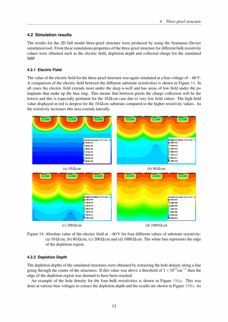
The value of the electric field for the three-pixel structure was again simulated at a bias voltage of �60 V.A comparison of the electric field between the different substrate resistivities is shown in Figure 14. Inall cases the electric field extends most under the deep n-well and has areas of low field under the p+implants that make up the bias ring. This means that between pixels the charge collection will be thelowest and this is especially pertinent for the 10 Wcm case due to very low field values. The high fieldvalue displayed in red is deepest for the 10 Wcm substrate compared to the higher resistivity values. Asthe resistivity increases this area extends laterally.
(a) 10 Wcm (b) 80 Wcm
(c) 200 Wcm (d) 1000 Wcm
Figure 14: Absolute value of the electric field at �60 V for four different values of substrate resistivity:(a) 10 Wcm, (b) 80 Wcm, (c) 200 Wcm and (d) 1000 Wcm. The white line represents the edgeof the depletion region.
4.2.2 Depletion Depth
The depletion depths of the simulated structures were obtained by extracting the hole density along a linegoing through the centre of the structures. If this value was above a threshold of 1⇥1012cm�3 then theedge of the depletion region was deemed to have been reached.
An example of the hole density for the four bulk resistivities is shown in Figure 15(a). This wasdone at various bias voltages to extract the depletion depth and the results are shown in Figure 15(b). As
12

4 Three-pixel structure
expected, increasing the applied bias and the bulk resistivity lead to a larger depletion region. To performa cross-check the expected values for the depletion depth of a standard diode, shown in dashed lines, arecompared. These values are computed from the following equation [8]:
w =
s2ere0
q
✓1
ND+
1NA
◆(V0 �V ) , (1)
where w is the depletion depth, er is the relative permittivity of the substrate, e0 is the vacuum permittiv-ity, q is the elementary charge, ND is the number of ionised donors, NA is the number of ionised acceptors,V0 is the built-in voltage and V is the applied bias voltage. There is a good agreement between the sim-ulation and prediction at 10 Wcm with the prediction being slightly larger. However as the resistivityincreases so does the difference between simulation and prediction. This is due to the assumptions madein Equation 1. One such assumption is that it is an infinitely large device consisting of a p-type side andan n-type side whereas in the simulations the n-type is segmented. The major effect is that the bias isapplied from the topside in the simulations and not the backside (as is the case in Equation 1), which hasa large influence on the depth. This results in the depletion depth being greater for backside biasing.
(a) (b)
Figure 15: (a) The hole density through the centre of the structures for different bulk resistivity values at�60 V. The dashed line is the threshold at which the edge of the depletion region is deemed.(b) Comparison of the depletion depth as a function of the square root of the bias voltagefor different bulk resistivity values. The dashed lines are the theoretical values for an abruptjunction.
4.2.3 Leakage current and capacitance
The leakage current of the three-pixel model at different bulk resistivities is shown in Figure 16(a). Asthe resistivity increases, so does the breakdown voltage. However the three cases with the larger valuesfor the bulk resistivity show a similar breakdown at around �100 V. This indicates that there is a limitingfactor stopping the breakdown voltage becoming larger than �100 V. One possible explanation is thatthe large electric fields found at the silicon oxide boundary on the surface of the device do not decreasewith resistivity. The greatest difference of the breakdown voltage is seen between the 10 Wcm and the80 Wcm models with a difference of around 10 V.
The value of the deep n-well-to-bulk capacitance of the three-pixel model was acquired using the samesimulation method as described in Section 3.2.2. This value, shown in Figure 16(b), for the four differentbulk resistivities shows smaller capacitances for higher resistivity substrates. This is expected because,
13

4 Three-pixel structure
as presented in Section 4.2.2, the larger resistivities have larger depletion regions. As with the leakagecurrent there is little difference between the three higher resistivity cases and the largest difference is from10 Wcm to 80 Wcm. The kink of the 80 Wcm and the 200 Wcm curves is produced when the depletionregion reaches the edge of the simulated structure.
(a) (b)
Figure 16: (a) Comparison of the leakage current as a function of bias voltage for the four different bulkresistivities. (b) Capacitance as a function of bias voltage at a frequency of 1 MHz for the fourbulk resistivities.
4.2.4 Response to Minimum Ionising Particle
Figure 17: Pulse shape of the simulated MIP passing through the centre of the central pixel cell fordifferent bulk resistivity values.
The method for generating the MIP signals of the three-pixel model is the same as the one described inSection 3.2.3. The pulse shape from the MIP signal is shown in Figure 17. The peak height decreasesfor larger resistivites and the peak times are approximatley the same (10–20 ps). At 0.5 ns the largerresistivities have larger current values. The collected charge of the simulations is found by integratingthe current over time; the resulting values are shown in Figure 18. The 1000 Wcm model has the highest
14
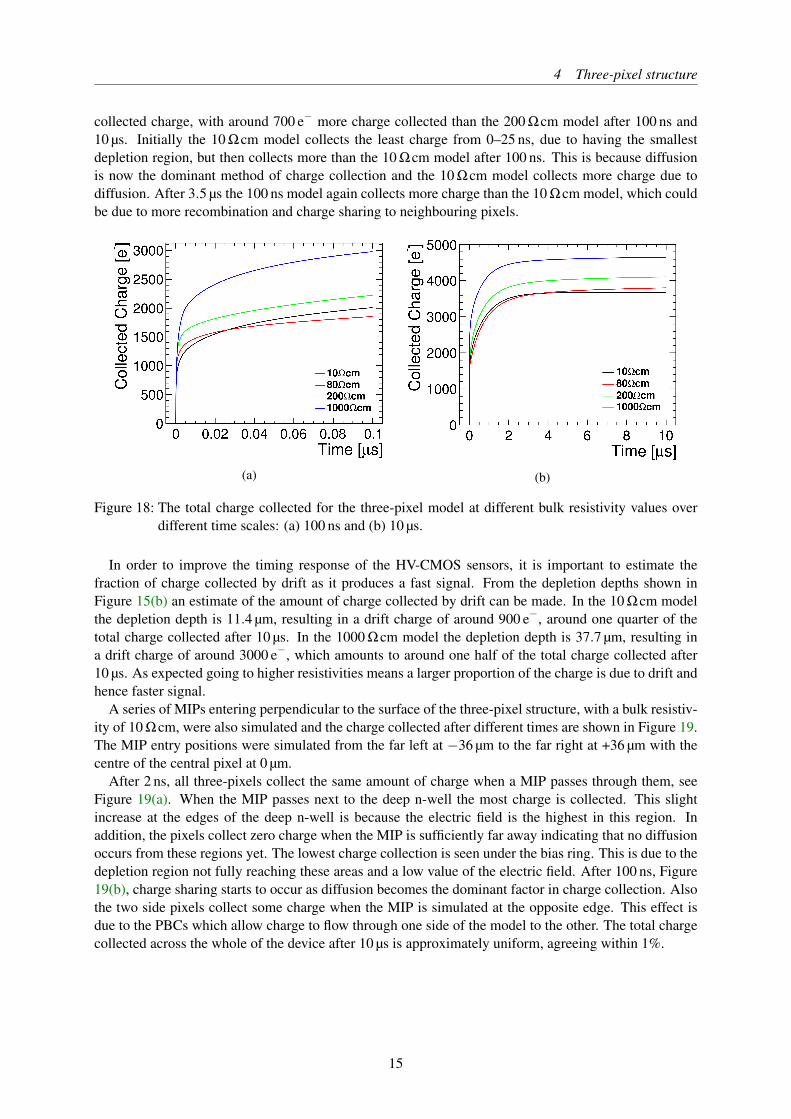
4 Three-pixel structure
collected charge, with around 700 e� more charge collected than the 200 Wcm model after 100 ns and10 µs. Initially the 10 Wcm model collects the least charge from 0–25 ns, due to having the smallestdepletion region, but then collects more than the 10 Wcm model after 100 ns. This is because diffusionis now the dominant method of charge collection and the 10 Wcm model collects more charge due todiffusion. After 3.5 µs the 100 ns model again collects more charge than the 10 Wcm model, which couldbe due to more recombination and charge sharing to neighbouring pixels.
(a) (b)
Figure 18: The total charge collected for the three-pixel model at different bulk resistivity values overdifferent time scales: (a) 100 ns and (b) 10 µs.
In order to improve the timing response of the HV-CMOS sensors, it is important to estimate thefraction of charge collected by drift as it produces a fast signal. From the depletion depths shown inFigure 15(b) an estimate of the amount of charge collected by drift can be made. In the 10 Wcm modelthe depletion depth is 11.4 µm, resulting in a drift charge of around 900 e�, around one quarter of thetotal charge collected after 10 µs. In the 1000 Wcm model the depletion depth is 37.7 µm, resulting ina drift charge of around 3000 e�, which amounts to around one half of the total charge collected after10 µs. As expected going to higher resistivities means a larger proportion of the charge is due to drift andhence faster signal.
A series of MIPs entering perpendicular to the surface of the three-pixel structure, with a bulk resistiv-ity of 10 Wcm, were also simulated and the charge collected after different times are shown in Figure 19.The MIP entry positions were simulated from the far left at �36 µm to the far right at +36 µm with thecentre of the central pixel at 0 µm.
After 2 ns, all three-pixels collect the same amount of charge when a MIP passes through them, seeFigure 19(a). When the MIP passes next to the deep n-well the most charge is collected. This slightincrease at the edges of the deep n-well is because the electric field is the highest in this region. Inaddition, the pixels collect zero charge when the MIP is sufficiently far away indicating that no diffusionoccurs from these regions yet. The lowest charge collection is seen under the bias ring. This is due to thedepletion region not fully reaching these areas and a low value of the electric field. After 100 ns, Figure19(b), charge sharing starts to occur as diffusion becomes the dominant factor in charge collection. Alsothe two side pixels collect some charge when the MIP is simulated at the opposite edge. This effect isdue to the PBCs which allow charge to flow through one side of the model to the other. The total chargecollected across the whole of the device after 10 µs is approximately uniform, agreeing within 1%.
15

5 Summary and Conclusions
(a) 2 ns (b) 100 ns
(c) 10 µs
Figure 19: The charge collected by each pixel and the sum of all three (total) for the three-pixel model,for different MIP positions along the surface of the structure. The results are for the samebulk resistivity of 10 Wcm at a bias of �60 V and for different integration times : (a) 2 ns, (b)100 ns and (c) 10 µs. The dashed lines represent the pixel boundaries.
5 Summary and Conclusions
In this study three TCAD simulation models of the CCPDv3 HV-CMOS sensor have been presented.A comparison between the 2D full model, the 2D reduced model and 3D reduced model has been con-ducted. Between all three models the absolute value of the electric field show similar trends to eachother. The breakdown voltage and the deep n-well-to-bulk capacitance values of the 2D full model areconsistent with 3D reduced model; both show good agreement with the breakdown voltage of the realdevice. In the charge collection for a MIP the difference between all models is around 10% after 100 nsbut reduces to less than 5% after 10 µs. Overall it is reasonable to use the 2D full model in place ofresource-intensive 3D simulations.
For the simulations of the 2D full three-pixel model the breakdown and depletion depth increase withresistivity while the capacitance reduces with resistivity. The larger resistivities collect more charge,with the 1000 Wcm model collecting around 50% more than the 10 Wcm model after 100 ns. There isadditionally a marked improvement in the charge collection time for higher resistivities. Once 100 nshave passed, the charge collection across the whole device is approximately uniform for every MIP entryposition. In all of the results there is a substantial improvement in performance for the higher resistivitydevices compared to the 10 Wcm model indicating the benefit of using a higher bulk resistivity.
The results produced by the TCAD simulations will be used as input at the start of a simulation chainthat contains the pixel electronics in the CCPDv3 chip, the coupling capacitance between the sensor andreadout ASIC and finally the circuitry inside the ASIC (CLICpix).
16

References
6 Acknowledgements
The author would like to thank M. Benoit, F. Di Bello and L. Meng for their input for the TCAD simu-lations as well as I. Peric, S. Kulis and I. Kremastiotis for their help in providing information about theCCPDv3 sensor chip.
References
[1] L. Linssen et al., Physics and Detectors at CLIC: CLIC Conceptual Design Report (2012),DOI: 10.5170/CERN-2012-003, arXiv: 1202.5940 [physics.ins-det].
[2] Synopsys TCAD,URL: http://www.synopsys.com/tools/tcad/Pages/default.aspx.
[3] I. Peric, Hybrid Pixel Particle-Detector Without Bump Interconnection,IEEE Trans. Nucl. Sci. 56 (2009) 519.
[4] I. Peric et al., High-voltage pixel detectors in commercial CMOS technologies for ATLAS,CLICand Mu3e experiments, Nucl. Instr. and Meth. A 731 (2013) 131.
[5] S. Feigl, Performance of capacitively coupled active pixel sensors in 180nm HV-CMOStechnology after irradiation to HL-LHC fluences, JINST 9 (2014) C03020.
[6] N. Alipour Tehrani et al.,Capacitively coupled hybrid pixel assemblies for the CLIC vertex detector,CLICdp-Pub-2015-003, CERN, 2015.
[7] Sentaurus Structure Editor: Device Editor and Process Emulator,URL: http://www.synopsys.com/tools/tcad/capsulemodule/sde_ds.pdf.
[8] S. M. Sze, Physics of semiconductor devices, 2nd ed., Wiley, New York, NY, 1981.
17