Embed Size (px)
Citation preview
Chin. Phys. B Vol. 24, No. 8 (2015) 086102
TOPICAL REVIEW — Silicene
Silicene: from monolayer to multilayer — A concise review∗
Li Hui(李 晖)†, Fu Hui-Xia(付会霞), and Meng Sheng(孟 胜)
Beijing National Laboratory for Condensed Matter Physics and Institute of Physics, Chinese Academy of Sciences, Beijing 100190, China
(Received 13 March 2015; revised manuscript received 20 May 2015; published online 20 July 2015)
Silicene, a newly isolated silicon allotrope with a two-dimensional (2D) honeycomb lattice structure, is predicted tohave electronic properties similar to those of graphene, including the existence of signature Dirac fermions. Furthermore,the strong spin–orbit interaction of Si atoms potentially makes silicene an experimentally accessible 2D topological in-sulator. Since 2012, silicene films have been experimentally synthesized on Ag (111) and other substrates, motivating aburst of research on silicene. We and collaborators have employed STM investigations and first principles calculations tointensively study the structure and electronic properties of silicene films on Ag (111), including monolayer, bilayer, andmultilayer silicenes, as well as hydrogenation of silicene.
Keywords: silicene, STM, STS, first principles calculation
PACS: 61.46.–w, 68.37.Ef, 73.22.–f, 81.05.Zx DOI: 10.1088/1674-1056/24/8/086102
1. Introduction
Graphene, a slice of sp2-bonded carbon film from bulkgraphite, has brought a storm of discoveries about two-dimensional (2D) materials in the last decade in the fields ofphysics, chemistry, and material science, due to graphene’sunique Dirac-type electronic structure and outstanding prop-erties such as high thermal and electrical conductivity, me-chanical stability, and inert chemical reactivity.[1] Beyondgraphene, people are searching for other elemental 2D materi-als. One attractive material is silicene, the one-atom-thick sili-con film with a honeycomb lattice, first predicted based on firstprinciples calculation.[2] Free-standing silicene adopts a low-buckled 2D structure with a buckling distance of ∼ 0.4 A. Assilicene is the silicon analog of graphene, many properties ofgraphene have been predicted also to exist for silicene, includ-ing the signature Dirac fermions. Furthermore, the predictedrelativistic Dirac fermions, which are due to spin orbital cou-pling (SOC) being stronger in silicon than in carbon, wouldmake single-layer silicene (SLS) a potential 2D topologicalinsulator, expected to yield an observable spin quantum-Halleffect.[3,4] Multilayer silicene (MLS) films also demonstrateinteresting electronic properties, such as chiral superconduct-ing behavior,[5] valley-polarized quantum Hall effect,[6] andelectronic structure that is dramatically tunable by varyingstacking modes.[7,8] It is also commonly proposed that siliceneis more compatible with silicon-based industry.
Within the past three years, great progress has also beenmade in the field of experimental synthesis of silicone.[9–29]
Unlike graphene, which can be exfoliated from van der Waals(vdW)-packed graphite, sp2-hybridized silicon does not existin nature. Thus, silicene can be achieved only by stabilizinginterfacial interaction with a substrate. So far, although growthif monolayer silicon film has been reported on several sub-strates such as ZrB2,[11] Ir (111),[12] and Ag (110),[23] morethan 90% of the research reports on silicene focus on siliceneepitaxially grown on Ag (111) surface.[9,10,13–22] Both SLSand MLS have been grown on Ag (111) surface using molec-ular beam epitaxy (MBE) and intensively studied by scan-ning tunneling microscopy (STM) and angle-resolved photoe-mission spectroscopy (ARPES), combined with first princi-ples calculations. However, the atomic structure of siliceneon Ag (111) is still under heavy debate, because it has beenfound that SLS can assume numerous metastable structureson Ag (111), depending on growth temperature and dynam-ics, such as 3×3, 2
√3× 2
√3, and
√3×√
3 surface recon-structions with respect to the Si (111)-1×1 lattice.[10] Amongthese reconstructions, the
√3×√
3-R30◦ structure is believedto be closest to isolated silicene, since it exhibits reversibledynamical phase transitions at low temperatures and weakerbonding to silver substrate[18,19,21] than other metastable struc-tures. Quasiparticle interference (QPI) pattern analysis[18] andARPES measurement[14] both reveal linear band dispersionsin such a
√3×√
3 structure. Recently, MLS structures havealso drawn much attention.[22–29] It has been found that MLScan form the unique
√3×√
3 structure only on Ag (111), andadopts a diamond-like stacking mode.[22,28] It is interestingthat such diamond-like silicon structures still exhibit a linear
∗Project supported by the National Natural Science Foundation of China (Grant Nos. 11334011, 11222431, and 11322431), the National Basic Research Programof China (Grant Nos. 2012CB921403, 2013CBA01600, and 2012CB921703), the “Strategic Priority Research Program” of the Chinese Academy of Sciences,and the Hundred Talents Program of Institute of Physics, Chinese Academy of Sciences.
†Corresponding author. E-mail: [email protected]© 2015 Chinese Physical Society and IOP Publishing Ltd http://iopscience.iop.org/cpb http://cpb.iphy.ac.cn
086102-1
Chin. Phys. B Vol. 24, No. 8 (2015) 086102
dispersion surface state, which is observed in both ARPES[24]
and QPI from STS.[22] Furthermore, it is remarkable that MLSis found to show great stability in air, while in contrast, SLS iseasily oxidized by oxygen and water.[26] The preserved Diracfermions and robustness in air indicate MLS has great poten-tial in practical applications of silicene.
On the other hand, silicon atoms in silicene have par-tial sp3-hybridization, displaying much higher reactivity thanpurely sp2-hybridized carbon atoms in graphene. Thus, sil-icene is easier to dope with other atoms, which can dramati-cally modify the electronic properties.[30–34] For example, firstprinciples calculations predict that hydrogenation can open alarge band gap (∼3 eV) for silicone,[30] and that halide-dopedsilicene can be a large-gap 2D topological insulator. Recentexperiment has confirmed silicene is much easier to be hydro-genated than grapheme.[34] The doped silicene also launchesa new field for making electronic devices based on silicene.
In this review, we will introduce previous theoretical pre-dictions of the structure of silicene (Section 2), the recent de-velopment of SLS and MLS grown on Ag (111) surface andother substrates (Section 3), as well as some of the newest re-sults on hydrogenated silicene (Section 4).
2. The properties of free-standing silicene2.1. Structure of monolayer silicene
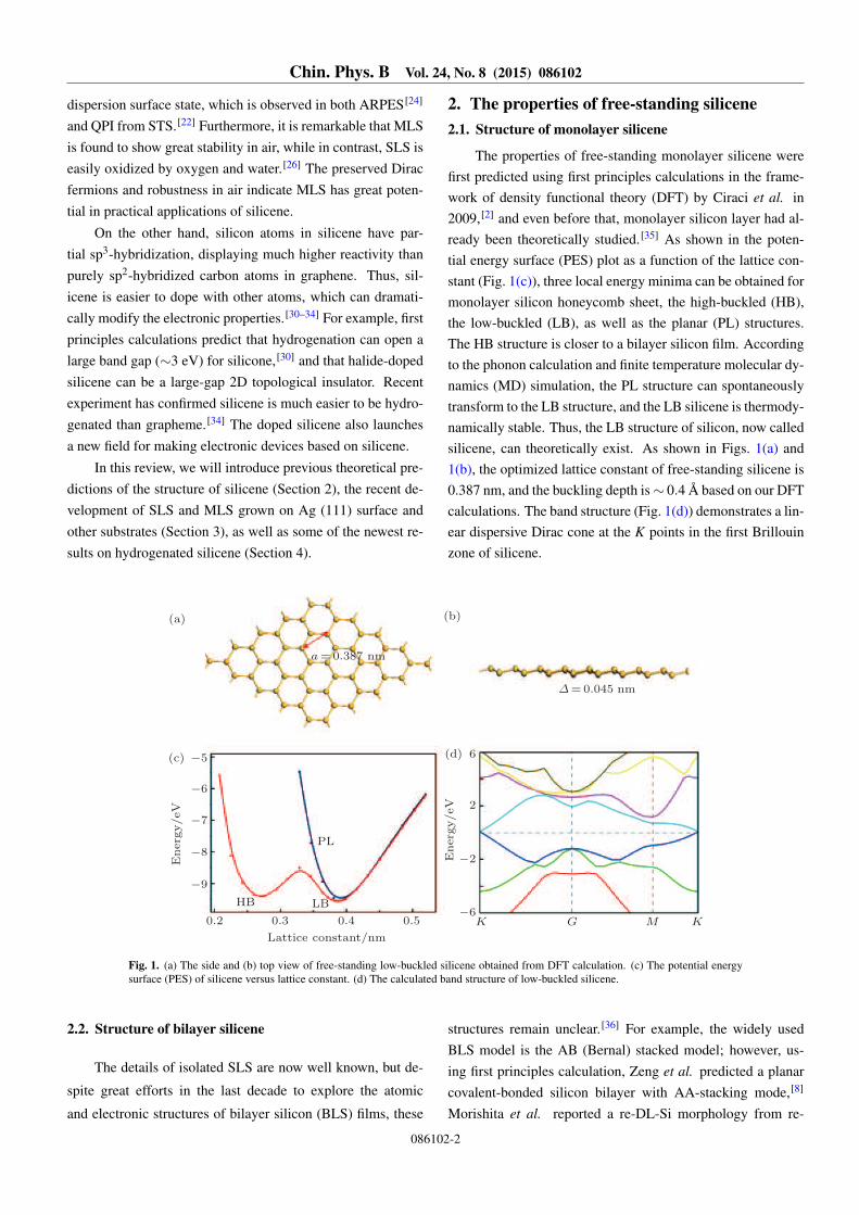
The properties of free-standing monolayer silicene werefirst predicted using first principles calculations in the frame-work of density functional theory (DFT) by Ciraci et al. in2009,[2] and even before that, monolayer silicon layer had al-ready been theoretically studied.[35] As shown in the poten-tial energy surface (PES) plot as a function of the lattice con-stant (Fig. 1(c)), three local energy minima can be obtained formonolayer silicon honeycomb sheet, the high-buckled (HB),the low-buckled (LB), as well as the planar (PL) structures.The HB structure is closer to a bilayer silicon film. Accordingto the phonon calculation and finite temperature molecular dy-namics (MD) simulation, the PL structure can spontaneouslytransform to the LB structure, and the LB silicene is thermody-namically stable. Thus, the LB structure of silicon, now calledsilicene, can theoretically exist. As shown in Figs. 1(a) and1(b), the optimized lattice constant of free-standing silicene is0.387 nm, and the buckling depth is∼ 0.4 A based on our DFTcalculations. The band structure (Fig. 1(d)) demonstrates a lin-ear dispersive Dirac cone at the K points in the first Brillouinzone of silicene.
a=0.387 nm
∆/. nm
-5
-6
-7
-8
-9
0.2 0.3 0.4 0.5
Lattice constant/nm
LBHB
PL
Energ
y/eV
Energ
y/eV
6
2
-2
-6K G M K
(d)(c)
(a) (b)
Fig. 1. (a) The side and (b) top view of free-standing low-buckled silicene obtained from DFT calculation. (c) The potential energysurface (PES) of silicene versus lattice constant. (d) The calculated band structure of low-buckled silicene.
2.2. Structure of bilayer silicene
The details of isolated SLS are now well known, but de-
spite great efforts in the last decade to explore the atomic
and electronic structures of bilayer silicon (BLS) films, these
structures remain unclear.[36] For example, the widely usedBLS model is the AB (Bernal) stacked model; however, us-ing first principles calculation, Zeng et al. predicted a planarcovalent-bonded silicon bilayer with AA-stacking mode,[8]
Morishita et al. reported a re-DL-Si morphology from re-
086102-2
Chin. Phys. B Vol. 24, No. 8 (2015) 086102
construction of two-layer Si (111) surface,[37] and Xiang et
al. predicted an Si-Cmme quasi-bilayer structure, using global
optimization.[38] It is well known that both interlayer interac-
tion and stacking order play key roles in determining the prop-
erties of multilayer silicene. Unlike van der Waals stacking in
bilayer graphene, whose global minimum is AB-stacked, BLS
has been proposed to have various morphologies due to com-
plicated interlayer covalent bonds.[39]
We employed a method similar to that used for study-
ing SLS to search for stable and functional BLS based on
DFT calculations.[7] The PBE functional[40] was employed for
structural research of BLS, and the HSE functional[41] was
used for electronic structure calculation. The projector aug-
mented wave (PAW) pseudopotentials combined with plane-
wave basis set (energy cutoff at 250 eV) were used with the
Vienna ab initio Simulation Package (VASP).[42] By scanning
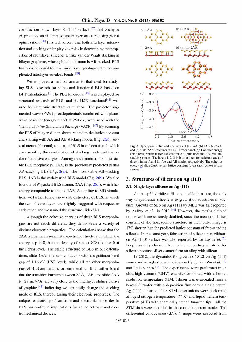
the PES of bilayer silicon sheets related to the lattice constant
and starting with AA and AB stacking modes (Fig. 2(e)), sev-
eral metastable configurations of BLS have been found, which
are named by the combination of stacking mode and the or-
der of cohesive energies. Among these minima, the most sta-
ble BLS morphology, 1AA, is the previously predicted planar
AA-stacking BLS (Fig. 2(a)). The most stable AB-stacking
BLS, 1AB is the widely used BLS model (Fig. 2(b)). We also
found a vdW-packed BLS isomer, 2AA (Fig. 2(c)), which has
energy comparable to that of 1AB. According to MD simula-
tion, we further found a new stable structure of BLS, in which
the two silicene layers are slightly staggered with respect to
each other, and we named the structure slide-2AA.
Although the cohesive energies of these BLS morpholo-
gies are not much different, they demonstrate a variety of
distinct electronic properties. The calculations show that the
2AA isomer has a semimetal electronic structure, in which the
energy gap is 0, but the density of state (DOS) is also 0 at
the Fermi level. The stable structure of BLS in our calcula-
tions, slide-2AA, is a semiconductor with a significant band
gap of 1.16 eV (HSE level), while all the other morpholo-
gies of BLS are metallic or semimetallic. It is further found
that the transition barriers between 2AA, 1AB, and slide-2AA
(∼ 29 meV/Si) are very close to the interlayer sliding barrier
of graphite,[43] indicating we can easily change the stacking
mode of BLS, thereby tuning their electronic properties. The
unique relationship of structure and electronic properties in
BLS has profound implications for nanoelectronic and elec-
tromechanical devices.
-3.7
-3.8
-3.9
-4.0
-4.1
2.4 3.0 3.6 4.2 4.8
Lattice constant/A
slide AA
Energ
y/(e
V/ato
m)
(e)
(a) 1AA
(c) 2AA (d) slide 2AA
(b) 1AB
Fig. 2. Upper panels: Top and side views of (a) 1AA, (b) 1AB, (c) 2AA,and (d) slide-2AA structures of BLS. Lower panel (e): Cohesive energy(PBE level) versus lattice constant for AA (blue line) and AB (red line)stacking modes. The labels 1, 2, 3 in blue and red fonts denote each ofthree minima found for AA and AB modes, respectively. The cohesiveenergy of slide-2AA versus lattice constant (cyan short curve) is alsoshown.[7]
3. Structures of silicene on Ag (111)3.1. Single layer silicene on Ag (111)
As the sp2-hybridized Si is not stable in nature, the onlyway to synthesize silicene is to grow it on substrates in vac-uum. Growth of SLS on Ag (111) by MBE was first reportedby Aufray et al. in 2010.[44] However, the results claimedin this work are seriously doubted, since the measured latticeconstant of the honeycomb structure in their STM image is17% shorter than the predicted lattice constant of free-standingsilicene. In the same year, fabrication of silicene nanoribbonson Ag (110) surface was also reported by Le Lay et al.[23]
People usually choose silver as the supporting substrate forsilicene because silver cannot form an alloy with silicon.
In 2012, the dynamics for growth of SLS on Ag (111)were convincingly studied independently by both Wu et al.[10]
and Le Lay et al.[14] The experiments were performed in anultra-high-vacuum (UHV) chamber combined with a home-made low-temperature STM. Silicon was evaporated from aheated Si wafer with a deposition flux onto a single-crystalAg (111) substrate. The STM observations were performedat liquid nitrogen temperature (77 K) and liquid helium tem-perature (4 K) with chemically etched tungsten tips. All theSTM data were recorded in the constant-current mode. Thedifferential conductance (dI/dV ) maps were extracted from
086102-3
Chin. Phys. B Vol. 24, No. 8 (2015) 086102
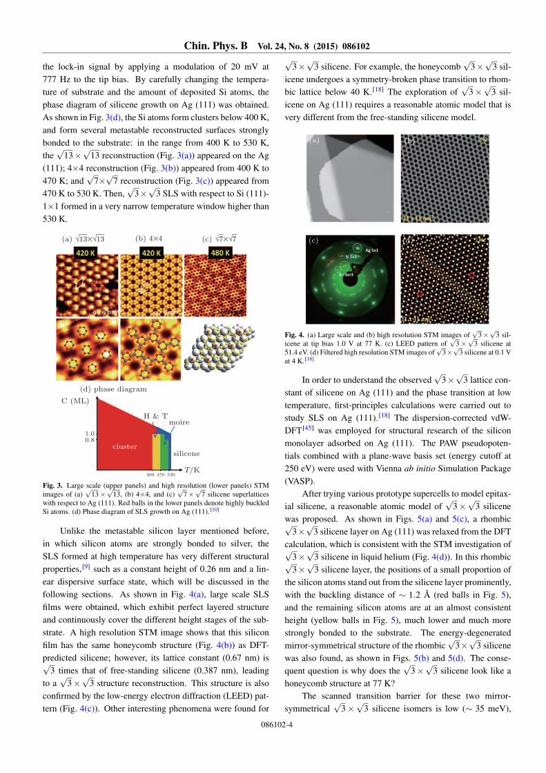
the lock-in signal by applying a modulation of 20 mV at777 Hz to the tip bias. By carefully changing the tempera-ture of substrate and the amount of deposited Si atoms, thephase diagram of silicene growth on Ag (111) was obtained.As shown in Fig. 3(d), the Si atoms form clusters below 400 K,and form several metastable reconstructed surfaces stronglybonded to the substrate: in the range from 400 K to 530 K,the√
13×√
13 reconstruction (Fig. 3(a)) appeared on the Ag(111); 4×4 reconstruction (Fig. 3(b)) appeared from 400 K to470 K; and
√7×√
7 reconstruction (Fig. 3(c)) appeared from470 K to 530 K. Then,
√3×√
3 SLS with respect to Si (111)-1×1 formed in a very narrow temperature window higher than530 K.
(d) phase diagram
C (ML)
1.00.8
400 530470T/K
H & Tmoire
silicene
(a) √13Τ√13 (c) √7Τ√7(b) 4Τ4
cluster
Fig. 3. Large scale (upper panels) and high resolution (lower panels) STMimages of (a)
√13×
√13, (b) 4×4, and (c)
√7×√
7 silicene superlatticeswith respect to Ag (111). Red balls in the lower panels denote highly buckledSi atoms. (d) Phase diagram of SLS growth on Ag (111).[10]
Unlike the metastable silicon layer mentioned before,in which silicon atoms are strongly bonded to silver, theSLS formed at high temperature has very different structuralproperties,[9] such as a constant height of 0.26 nm and a lin-ear dispersive surface state, which will be discussed in thefollowing sections. As shown in Fig. 4(a), large scale SLSfilms were obtained, which exhibit perfect layered structureand continuously cover the different height stages of the sub-strate. A high resolution STM image shows that this siliconfilm has the same honeycomb structure (Fig. 4(b)) as DFT-predicted silicene; however, its lattice constant (0.67 nm) is√
3 times that of free-standing silicene (0.387 nm), leadingto a√
3×√
3 structure reconstruction. This structure is alsoconfirmed by the low-energy electron diffraction (LEED) pat-tern (Fig. 4(c)). Other interesting phenomena were found for
√3×√
3 silicene. For example, the honeycomb√
3×√
3 sil-icene undergoes a symmetry-broken phase transition to rhom-bic lattice below 40 K.[18] The exploration of
√3×√
3 sil-icene on Ag (111) requires a reasonable atomic model that isvery different from the free-standing silicene model.
(a) (b)
(c) (d)
Fig. 4. (a) Large scale and (b) high resolution STM images of√
3×√
3 sil-icene at tip bias 1.0 V at 77 K. (c) LEED pattern of
√3×√
3 silicene at51.4 eV. (d) Filtered high resolution STM images of
√3×√
3 silicene at 0.1 Vat 4 K.[18]
In order to understand the observed√
3×√
3 lattice con-stant of silicene on Ag (111) and the phase transition at lowtemperature, first-principles calculations were carried out tostudy SLS on Ag (111).[18] The dispersion-corrected vdW-DFT[45] was employed for structural research of the siliconmonolayer adsorbed on Ag (111). The PAW pseudopoten-tials combined with a plane-wave basis set (energy cutoff at250 eV) were used with Vienna ab initio Simulation Package(VASP).
After trying various prototype supercells to model epitax-ial silicene, a reasonable atomic model of
√3×√
3 silicenewas proposed. As shown in Figs. 5(a) and 5(c), a rhombic√
3×√
3 silicene layer on Ag (111) was relaxed from the DFTcalculation, which is consistent with the STM investigation of√
3×√
3 silicene in liquid helium (Fig. 4(d)). In this rhombic√3×√
3 silicene layer, the positions of a small proportion ofthe silicon atoms stand out from the silicene layer prominently,with the buckling distance of ∼ 1.2 A (red balls in Fig. 5),and the remaining silicon atoms are at an almost consistentheight (yellow balls in Fig. 5), much lower and much morestrongly bonded to the substrate. The energy-degeneratedmirror-symmetrical structure of the rhombic
√3×√
3 silicenewas also found, as shown in Figs. 5(b) and 5(d). The conse-quent question is why does the
√3×√
3 silicene look like ahoneycomb structure at 77 K?
The scanned transition barrier for these two mirror-symmetrical
√3×√
3 silicene isomers is low (∼ 35 meV),
086102-4
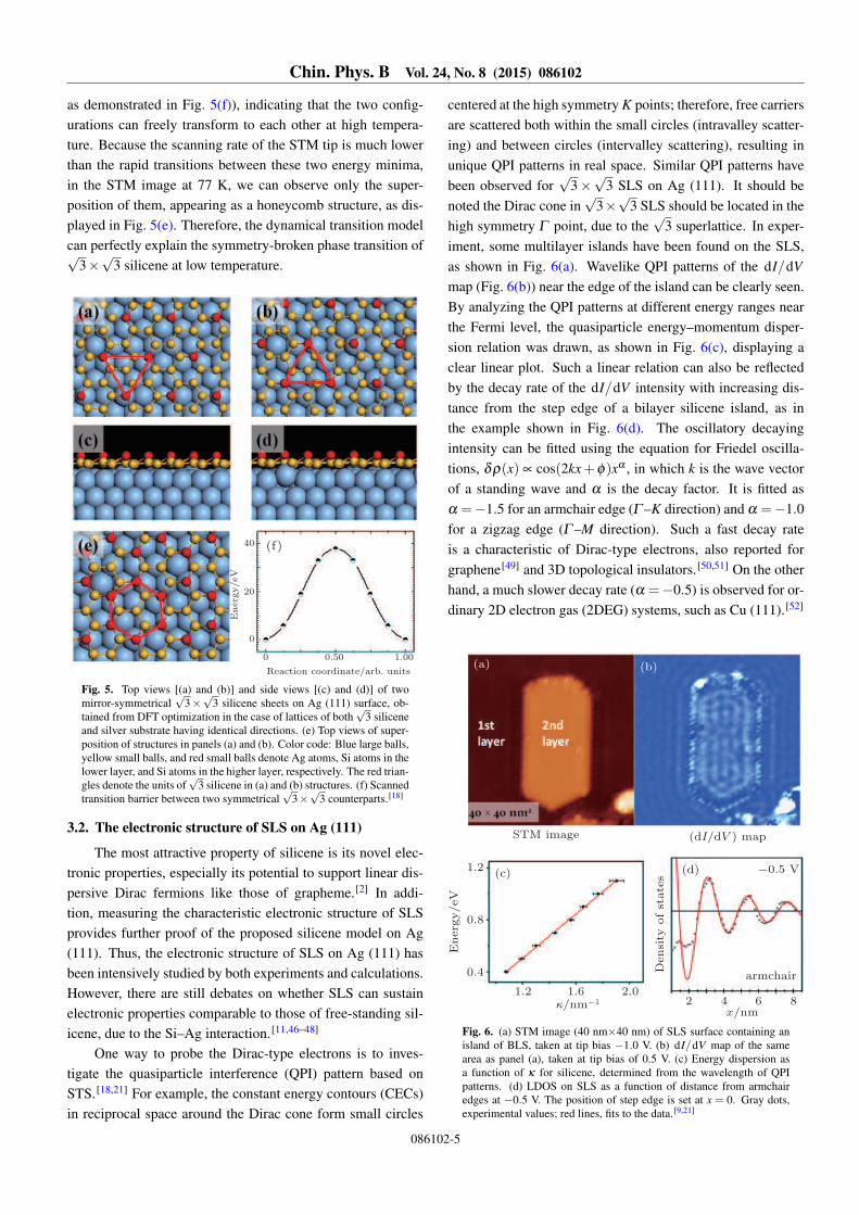
Chin. Phys. B Vol. 24, No. 8 (2015) 086102
as demonstrated in Fig. 5(f)), indicating that the two config-urations can freely transform to each other at high tempera-ture. Because the scanning rate of the STM tip is much lowerthan the rapid transitions between these two energy minima,in the STM image at 77 K, we can observe only the super-position of them, appearing as a honeycomb structure, as dis-played in Fig. 5(e). Therefore, the dynamical transition modelcan perfectly explain the symmetry-broken phase transition of√
3×√
3 silicene at low temperature.
40
20
0
0 0.50 1.00
Reaction coordinate/arb. units
Energ
y/eV
(f)
Fig. 5. Top views [(a) and (b)] and side views [(c) and (d)] of twomirror-symmetrical
√3×√
3 silicene sheets on Ag (111) surface, ob-tained from DFT optimization in the case of lattices of both
√3 silicene
and silver substrate having identical directions. (e) Top views of super-position of structures in panels (a) and (b). Color code: Blue large balls,yellow small balls, and red small balls denote Ag atoms, Si atoms in thelower layer, and Si atoms in the higher layer, respectively. The red trian-gles denote the units of
√3 silicene in (a) and (b) structures. (f) Scanned
transition barrier between two symmetrical√
3×√
3 counterparts.[18]
3.2. The electronic structure of SLS on Ag (111)
The most attractive property of silicene is its novel elec-tronic properties, especially its potential to support linear dis-persive Dirac fermions like those of grapheme.[2] In addi-tion, measuring the characteristic electronic structure of SLSprovides further proof of the proposed silicene model on Ag(111). Thus, the electronic structure of SLS on Ag (111) hasbeen intensively studied by both experiments and calculations.However, there are still debates on whether SLS can sustainelectronic properties comparable to those of free-standing sil-icene, due to the Si–Ag interaction.[11,46–48]
One way to probe the Dirac-type electrons is to inves-tigate the quasiparticle interference (QPI) pattern based onSTS.[18,21] For example, the constant energy contours (CECs)in reciprocal space around the Dirac cone form small circles
centered at the high symmetry K points; therefore, free carriersare scattered both within the small circles (intravalley scatter-ing) and between circles (intervalley scattering), resulting inunique QPI patterns in real space. Similar QPI patterns havebeen observed for
√3×√
3 SLS on Ag (111). It should benoted the Dirac cone in
√3×√
3 SLS should be located in thehigh symmetry Γ point, due to the
√3 superlattice. In exper-
iment, some multilayer islands have been found on the SLS,as shown in Fig. 6(a). Wavelike QPI patterns of the dI/dVmap (Fig. 6(b)) near the edge of the island can be clearly seen.By analyzing the QPI patterns at different energy ranges nearthe Fermi level, the quasiparticle energy–momentum disper-sion relation was drawn, as shown in Fig. 6(c), displaying aclear linear plot. Such a linear relation can also be reflectedby the decay rate of the dI/dV intensity with increasing dis-tance from the step edge of a bilayer silicene island, as inthe example shown in Fig. 6(d). The oscillatory decayingintensity can be fitted using the equation for Friedel oscilla-tions, δρ(x) ∝ cos(2kx+φ)xα , in which k is the wave vectorof a standing wave and α is the decay factor. It is fitted asα =−1.5 for an armchair edge (Γ –K direction) and α =−1.0for a zigzag edge (Γ –M direction). Such a fast decay rateis a characteristic of Dirac-type electrons, also reported forgraphene[49] and 3D topological insulators.[50,51] On the otherhand, a much slower decay rate (α =−0.5) is observed for or-dinary 2D electron gas (2DEG) systems, such as Cu (111).[52]
(a) (b)
STM image (dI/dV ) map
.
.
.
.
. .
κ/nm-1
x/nm
-0.5 V
Densi
ty o
f st
ate
s
Energ
y/eV
(c) (d)
armchair
Fig. 6. (a) STM image (40 nm×40 nm) of SLS surface containing anisland of BLS, taken at tip bias −1.0 V. (b) dI/dV map of the samearea as panel (a), taken at tip bias of 0.5 V. (c) Energy dispersion asa function of κ for silicene, determined from the wavelength of QPIpatterns. (d) LDOS on SLS as a function of distance from armchairedges at −0.5 V. The position of step edge is set at x = 0. Gray dots,experimental values; red lines, fits to the data.[9,21]
086102-5
Chin. Phys. B Vol. 24, No. 8 (2015) 086102
The Dirac cone in the band structure of distorted√
3×√
3silicene is also confirmed by first principles calculations.[18,21]
As shown in Fig. 7(a), the band structure of isolated√
3×√
3distorted silicene is similar to that of 1×1 silicene (Fig. 7(b)).However, there is a small band gap (∼0.15 eV) at the Diraccone, and a flat band within the gap is contributed by the high-buckled Si atoms. Another interesting characteristic for elec-tronic structure of
√3×√
3 silicene is that its Dirac cone islocated at the Γ point, which has six-fold symmetry, insteadof the Dirac cone for graphene, located at the three-fold sym-metric K point. As a result, at the high energy region of theDirac cone for
√3×√
3 silicene, we should observe hexago-nal energy warping. Such hexagonal warping is confirmed byboth DFT calculation (Fig. 7(c)) and fast Fourier transform ofthe dI/dV map. The linear dispersive bands of SLS on Ag(111) were also observed by ARPES measurement.[14]
2
0
-2K KΓ Μ K KΓ Μ
0.4
0.4
0.2
0
0
−0.2
−0.4−0.4
0.5
0.750
(d)BZ
K
M
-0.9 V
(b)(a)
(c)
Energ
y/eV
ky
kx
2
0
-2
Energ
y/eV
Fig. 7. (a) and (b) Band structures of the√
3×√
3 structure of sil-icene layer and 1× 1 structure of free-standing silicene, respectively.(c) Constant energy contours of the Dirac cone of
√3×√
3 SLS fromDFT calculations. (d) A k-space map obtained by Fourier transformof the dI/dV map at voltages of −0.9 V. The hexagon of 1×1 BZ issuperimposed.[18,21]
3.3. SLS on other substrates
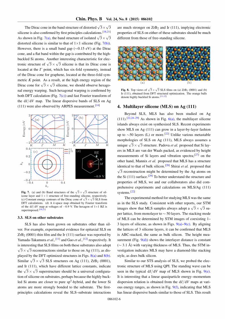
SLS has also been grown on substrates other than sil-ver. For example, experimental evidence for epitaxial SLS onZrB2 (0001) thin film and the Ir (111) surface was reported byYamada-Takamura et al.,[11] and Gao et al.,[12] respectively. Itis interesting that SLS films on both these substrates also adopt√
3×√
3 reconstructions similar to those on Ag (111), as dis-played by the DFT optimized structures in Figs. 8(a) and 8(b).Similar
√3×√
3 SLS structures on Ag (111), ZrB2 (0001),and Ir (111), which have different lattice constants, indicatethe√
3×√
3 superstructure should be a universal configura-tion of silicene on substrates, perhaps because the highly buck-led Si atoms are closer to pure sp3-hybrid, and the lower Siatoms are more strongly bonded to the substrate. The first-principles calculations reveal the SLS–substrate interactions
are much stronger on ZrB2 and Ir (111), implying electronicproperties of SLS on either of these substrates should be muchdifferent from those of free-standing silicene.
(a) (b)
Fig. 8. Top views of√
3×√
3 SLS films on (a) ZrB2 (0001) and (b)Ir (111), obtained from DFT structural optimization. The orange ballsdenote highly buckled Si atoms.[11,12]
4. Multilayer silicene (MLS) on Ag (111)Beyond SLS, MLS has also been studied on Ag
(111).[22,24–29] As shown in Fig. 6(a), the multilayer siliceneislands always exist on synthesized SLS. Recent experimentsshow MLS on Ag (111) can grow in a layer-by-layer fashionup to ∼50 layers (L) or more.[22] Unlike various metastablemorphologies of SLS on Ag (111), MLS always assumes aunique
√3×√
3 structure. Padova et al. proposed that Si lay-ers in MLS are van der Waals packed, as evidenced by heightmeasurements of Si layers and vibration spectra;[27] on theother hand, Mannix et al. proposed that MLS has a structureidentical to that of bulk silicon.[28] Shirai et al. proposed that√
3 reconstruction might be determined by the Ag atoms onthe Si (111) surface.[29] To better understand the structure andproperties of MLS, we and our collaborators also did com-prehensive experiments and calculations on MLS/Ag (111)systems.[22]
The experimental method for studying MLS was the sameas in the SLS study. Consistent with other reports, our STMimages show that MLS samples always adopt a
√3×√
3 su-per lattice, from monolayer to∼ 50 layers. The stacking modeof MLS can be determined by STM images of coexisting 1–3 layers of silicene, as shown in Figs. 9(a)–9(c). By aligningthe lattices of 3 silicene layers, it can be confirmed that MLSis ABC-stacked, the same as bulk silicon. The height mea-surement (Fig. 9(d)) shows the interlayer distance is constant(∼ 3.1 A) with varying thickness of MLS. Thus, the STM in-vestigation indicates MLS may have a diamond-like stackingstyle, as does bulk silicon.
Similar to our STS analysis of SLS, we probed the elec-tronic structure of MLS using QPI. The standing wave can beseen in the typical dI/dV map of MLS shown in Fig. 9(e).It is interesting that a linear quasiparticle energy–momentumdispersion relation is obtained from the dI/dV maps at vari-ous energy ranges, as shown in Fig. 9(f), indicating that MLShas linear dispersive bands similar to those of SLS. This result
086102-6
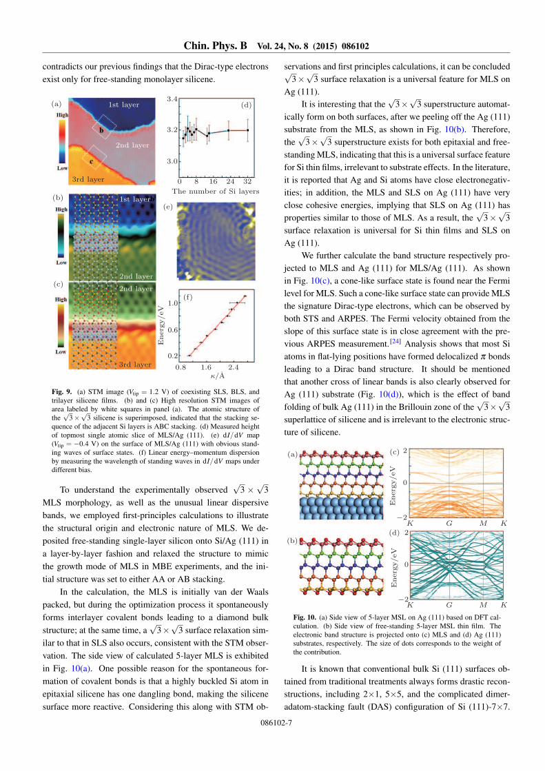
Chin. Phys. B Vol. 24, No. 8 (2015) 086102
contradicts our previous findings that the Dirac-type electronsexist only for free-standing monolayer silicene.
3.4
3.2
3.0
0 8 16 24 32
The number of Si layers
0.8 1.6 2.4κ/A
1.0
0.6
0.2
Energ
y/eV
3rd layer
2nd layer
2nd layer
1st layer
2nd layer
3rd layer
1st layer (d)(a)
(b)
(c)
(f)
(e)
Fig. 9. (a) STM image (Vtip = 1.2 V) of coexisting SLS, BLS, andtrilayer silicene films. (b) and (c) High resolution STM images ofarea labeled by white squares in panel (a). The atomic structure ofthe√
3×√
3 silicene is superimposed, indicated that the stacking se-quence of the adjacent Si layers is ABC stacking. (d) Measured heightof topmost single atomic slice of MLS/Ag (111). (e) dI/dV map(Vtip = −0.4 V) on the surface of MLS/Ag (111) with obvious stand-ing waves of surface states. (f) Linear energy–momentum dispersionby measuring the wavelength of standing waves in dI/dV maps underdifferent bias.
To understand the experimentally observed√
3 ×√
3MLS morphology, as well as the unusual linear dispersivebands, we employed first-principles calculations to illustratethe structural origin and electronic nature of MLS. We de-posited free-standing single-layer silicon onto Si/Ag (111) ina layer-by-layer fashion and relaxed the structure to mimicthe growth mode of MLS in MBE experiments, and the ini-tial structure was set to either AA or AB stacking.
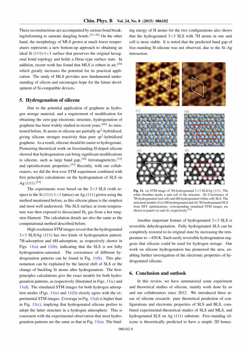
In the calculation, the MLS is initially van der Waalspacked, but during the optimization process it spontaneouslyforms interlayer covalent bonds leading to a diamond bulkstructure; at the same time, a
√3×√
3 surface relaxation sim-ilar to that in SLS also occurs, consistent with the STM obser-vation. The side view of calculated 5-layer MLS is exhibitedin Fig. 10(a). One possible reason for the spontaneous for-mation of covalent bonds is that a highly buckled Si atom inepitaxial silicene has one dangling bond, making the silicenesurface more reactive. Considering this along with STM ob-
servations and first principles calculations, it can be concluded√3×√
3 surface relaxation is a universal feature for MLS onAg (111).
It is interesting that the√
3×√
3 superstructure automat-ically form on both surfaces, after we peeling off the Ag (111)substrate from the MLS, as shown in Fig. 10(b). Therefore,the√
3×√
3 superstructure exists for both epitaxial and free-standing MLS, indicating that this is a universal surface featurefor Si thin films, irrelevant to substrate effects. In the literature,it is reported that Ag and Si atoms have close electronegativ-ities; in addition, the MLS and SLS on Ag (111) have veryclose cohesive energies, implying that SLS on Ag (111) hasproperties similar to those of MLS. As a result, the
√3×√
3surface relaxation is universal for Si thin films and SLS onAg (111).
We further calculate the band structure respectively pro-jected to MLS and Ag (111) for MLS/Ag (111). As shownin Fig. 10(c), a cone-like surface state is found near the Fermilevel for MLS. Such a cone-like surface state can provide MLSthe signature Dirac-type electrons, which can be observed byboth STS and ARPES. The Fermi velocity obtained from theslope of this surface state is in close agreement with the pre-vious ARPES measurement.[24] Analysis shows that most Siatoms in flat-lying positions have formed delocalized π bondsleading to a Dirac band structure. It should be mentionedthat another cross of linear bands is also clearly observed forAg (111) substrate (Fig. 10(d)), which is the effect of bandfolding of bulk Ag (111) in the Brillouin zone of the
√3×√
3superlattice of silicene and is irrelevant to the electronic struc-ture of silicene.
2
0
-2
(d)
(c)(a)
(b)
Energy/eV
2
0
-2
Energy/eV
K G M K
K G M K
Fig. 10. (a) Side view of 5-layer MSL on Ag (111) based on DFT cal-culation. (b) Side view of free-standing 5-layer MSL thin film. Theelectronic band structure is projected onto (c) MLS and (d) Ag (111)substrates, respectively. The size of dots corresponds to the weight ofthe contribution.
It is known that conventional bulk Si (111) surfaces ob-tained from traditional treatments always forms drastic recon-structions, including 2×1, 5×5, and the complicated dimer-adatom-stacking fault (DAS) configuration of Si (111)-7×7.
086102-7
Chin. Phys. B Vol. 24, No. 8 (2015) 086102
These reconstructions are accompanied by serious bond break-ing/reforming to saturate dangling bonds.[53–59] On the otherhand, the morphology of MLS grown at much lower temper-atures represents a new bottom-up approach to obtaining anideal Si (111)-1×1 surface that preserves the original hexag-onal bond topology and holds a Dirac-type surface state. Inaddition, recent work has found that MLS is robust in air,[26]
which greatly increases the potential for its practical appli-cation. The study of MLS provides new fundamental under-standing of silicon and encourages hope for the future devel-opment of Si-compatible devices.
5. Hydrogenation of siliceneDue to the potential application of graphene as hydro-
gen storage material, and a requirement of modification forobtaining the zero-gap electronic structure, hydrogenation ofgraphene has been widely studied in recent years.[60] As men-tioned before, Si atoms in silicene are partially sp3-hybridized,giving silicene stronger reactivity than pure sp2-hybridizedgraphene. As a result, silicene should be easier to hydrogenate.Pioneering theoretical work on freestanding H-doped siliceneshowed that hydrogenation can bring significant modificationsto silicene, such as large band gap,[30] ferromagneticity,[32]
and optoelectronic properties.[33] Recently, with our collab-orators, we did the first-ever STM experiment combined withfirst principles calculations on the hydrogenation of SLS onAg (111).[34]
The experiments were based on the 3×3 SLS (with re-spect to the Si (111)-1×1 lattice) on Ag (111) grown using themethod mentioned before, as this silicene phase is the simplestand most well understood. The SLS surface at room tempera-ture was then exposed to dissociated H2 gas from a hot tung-sten filament. The calculation details are also the same as thecomputational method described before.
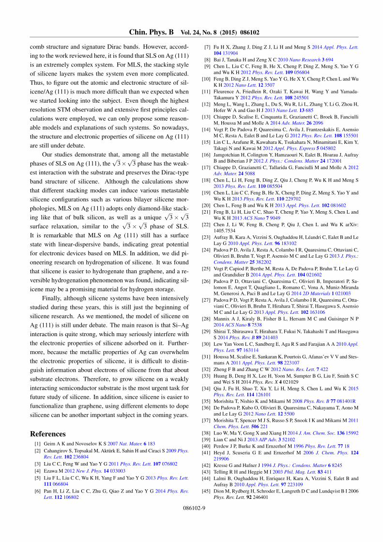
High resolution STM images reveal that the hydrogenated3×3 SLS/Ag (111) has two kinds of hydrogenation pattern:7H-adsorption and 6H-adsorption, as respectively shown inFigs. 11(a) and 11(b), indicating that the SLS is not fullyhydrogenation-saturated. The coexistence of different hy-drogenation patterns can be found in Fig. 11(b). This phe-nomenon can be explained by the lateral shift of SLS or thechange of buckling Si atoms after hydrogenation. The first-principles calculations give the exact models for both hydro-genation patterns, as respectively illustrated in Figs. 11(c) and11(d). The simulated STM images for both hydrogen adsorp-tion modes (Figs. 11(e) and 11(f)) closely agree with the ex-perimental STM images. Coverage in Fig. 11(d) is higher thanin Fig. 11(c), implying that hydrogenated silicene prefers toadopt the latter structure in a hydrogen atmosphere. This isconsistent with the experimental observation that most hydro-genation patterns are the same as that in Fig. 11(a). The bind-
ing energy of H atoms for the two configurations also showsthat the hydrogenated 3×3 SLS with 7H atoms in one unitcell is more stable. It is noted that the predicted band gap offree-standing H-silicene was not observed, due to the Si–Aginteraction.
(d)(c)
(e) (f)
(b)(a)
Fig. 11. (a) STM image of 7H-hydrogenated 3×3 SLS/Ag (111). Thewhite rhombus marks a unit cell of the structure. (b) Coexistence of7H-hydrogenated (red cell) and 6H-hydrogenated (white cell) SLS. Thestructural models of (c) 6H-hydrogenated and (d) 7H-hydrogenated SLSfrom DFT optimizations; corresponding simulated STM images areshown in panels (e) and (f), respectively.[34]
Another important feature of hydrogenated 3×3 SLS isreversible dehydrogenation. Fully hydrogenated SLS can becompletely restored to its original state by increasing the tem-perature to∼450 K. Such easily reversible hydrogenation sug-gests that silicene could be used for hydrogen storage. Ourwork on silicene hydrogenation has pioneered the area, en-abling further investigation of the electronic properties of hy-drogenated silicene.
6. Conclusion and outlookIn this review, we have summarized some experiment
and theoretical studies of silicene, mainly work done by usand our collaborators since 2012. We introduced three ar-eas of silicene research: pure theoretical prediction of con-figurations and electronic properties of SLS and BLS, com-bined experimental-theoretical studies of SLS and MLS, andhydrogenated SLS on Ag (111) substrate. Free-standing sil-icene is theoretically predicted to have a simple 2D honey-
086102-8
Chin. Phys. B Vol. 24, No. 8 (2015) 086102
comb structure and signature Dirac bands. However, accord-ing to the work reviewed here, it is found that SLS on Ag (111)is an extremely complex system. For MLS, the stacking styleof silicene layers makes the system even more complicated.Thus, to figure out the atomic and electronic structure of sil-icene/Ag (111) is much more difficult than we expected whenwe started looking into the subject. Even though the highestresolution STM observation and extensive first principles cal-culations were employed, we can only propose some reason-able models and explanations of such systems. So nowadays,the structure and electronic properties of silicene on Ag (111)are still under debate.
Our studies demonstrate that, among all the metastablephases of SLS on Ag (111), the
√3×√
3 phase has the weak-est interaction with the substrate and preserves the Dirac-typeband structure of silicene. Although the calculations showthat different stacking modes can induce various metastablesilicene configurations such as various bilayer silicene mor-phologies, MLS on Ag (111) adopts only diamond-like stack-ing like that of bulk silicon, as well as a unique
√3×√
3surface relaxation, similar to the
√3×√
3 phase of SLS.It is remarkable that MLS on Ag (111) still has a surfacestate with linear-dispersive bands, indicating great potentialfor electronic devices based on MLS. In addition, we did pi-oneering research on hydrogenation of silicene. It was foundthat silicene is easier to hydrogenate than graphene, and a re-versible hydrogenation phenomenon was found, indicating sil-icene may be a promising material for hydrogen storage.
Finally, although silicene systems have been intensivelystudied during these years, this is still just the beginning ofsilicene research. As we mentioned, the model of silicene onAg (111) is still under debate. The main reason is that Si–Aginteraction is quite strong, which may seriously interfere withthe electronic properties of silicene adsorbed on it. Further-more, because the metallic properties of Ag can overwhelmthe electronic properties of silicene, it is difficult to distin-guish information about electrons of silicene from that aboutsubstrate electrons. Therefore, to grow silicene on a weaklyinteracting semiconductor substrate is the most urgent task forfuture study of silicene. In addition, since silicene is easier tofunctionalize than graphene, using different elements to dopesilicene can be another important subject in the coming years.
References[1] Geim A K and Novoselov K S 2007 Nat. Mater. 6 183[2] Cahangirov S, Topsakal M, Akturk E, Sahin H and Ciraci S 2009 Phys.
Rev. Lett. 102 236804[3] Liu C C, Feng W and Yao Y G 2011 Phys. Rev. Lett. 107 076802[4] Ezawa M 2012 New J. Phys. 14 033003[5] Liu F L, Liu C C, Wu K H, Yang F and Yao Y G 2013 Phys. Rev. Lett.
111 066804[6] Pan H, Li Z, Liu C C, Zhu G, Qiao Z and Yao Y G 2014 Phys. Rev.
Lett. 112 106802
[7] Fu H X, Zhang J, Ding Z J, Li H and Meng S 2014 Appl. Phys. Lett.104 131904
[8] Bai J, Tanaka H and Zeng X C 2010 Nano Research 3 694[9] Chen L, Liu C C, Feng B, He X, Cheng P, Ding Z, Meng S, Yao Y G
and Wu K H 2012 Phys. Rev. Lett. 109 056804[10] Feng B, Ding Z J, Meng S, Yao Y G, He X Y, Cheng P, Chen L and Wu
K H 2012 Nano Lett. 12 3507[11] Fleurence A, Friedlein R, Ozaki T, Kawai H, Wang Y and Yamada-
Takamura Y 2012 Phys. Rev. Lett. 108 245501[12] Meng L, Wang L, Zhang L, Du S, Wu R, Li L, Zhang Y, Li G, Zhou H,
Hofer W A and Gao H J 2013 Nano Lett. 13 685[13] Chiappe D, Scalise E, Cinquanta E, Grazianetti C, Broek B, Fanciulli
M, Houssa M and Molle A 2014 Adv. Mater. 26 2096[14] Vogt P, De Padova P, Quaresima C, Avila J, Frantzeskakis E, Asensio
M C, Resta A, Ealet B and Le Lay G 2012 Phys. Rev. Lett. 108 155501[15] Lin C L, Arafune R, Kawahara K, Tsukahara N, Minamitani E, Kim Y,
Takagi N and Kawai M 2012 Appl. Phys. Express 5 045802[16] Jamgotchian H, Colington Y, Hamzaouri N, Ealet B, Hoarau J, Aufray
B and Biberian J P 2012 J. Phys.: Condens. Matter 24 172001[17] Chiappe D, Grazianetti C, Tallarida G, Fanciulli M and Molle A 2012
Adv. Mater. 24 5088[18] Chen L, Li H, Feng B, Ding Z, Qiu J, Cheng P, Wu K H and Meng S
2013 Phys. Rev. Lett. 110 085504[19] Chen L, Liu C C, Feng B, He X, Cheng P, Ding Z, Meng S, Yao Y and
Wu K H 2013 Phys. Rev. Lett. 110 229702[20] Chen L, Feng B and Wu K H 2013 Appl. Phys. Lett. 102 081602[21] Feng B, Li H, Liu C C, Shao T, Cheng P, Yao Y, Meng S, Chen L and
Wu K H 2013 ACS Nano 7 9049[22] Chen J, Li W, Feng B, Cheng P, Qiu J, Chen L and Wu K arXiv:
1405.7534[23] Aufray B, Kara A, Vizzini S, Oughaddou H, Leandri C, Ealet B and Le
Lay G 2010 Appl. Phys. Lett. 96 183102[24] Padova P D, Avila J, Resta A, Colambo I R, Quaresima C, Ottaviani C,
Olivieri B, Bruhn T, Vogt P, Asensio M C and Le Lay G 2013 J. Phys.:Condens. Matter 25 382202
[25] Vogt P, Capiod P, Berthe M, Resta A, De Padova P, Bruhn T, Le Lay Gand Grandidier B 2014 Appl. Phys. Lett. 104 021602
[26] Padova P D, Ottaviani C, Quaresima C, Olivieri B, Imperatori P, Sa-lomon E, Angot T, Quagliano L, Romano C, Vona A, Muniz-MirandaM, Generosi A, Paci B and Le Lay G 2014 2D Materials 1 021003
[27] Padova P D, Vogt P, Resta A, Avila J, Colambo I R, Quaresima C, Otta-viani C, Olivieri B, Bruhn T, Hirahara T, Shirai T, Hasegawa S, AsensioM C and Le Lay G 2013 Appl. Phys. Lett. 102 163106
[28] Mannix A J, Kiraly B, Fisher B L, Hersam M C and Guisinger N P2014 ACS Nano 8 7538
[29] Shirai T, Shirasawa T, Hirahara T, Fukui N, Takahashi T and HasegawaS 2014 Phys. Rev. B 89 241403
[30] Lew Yan Voon L C, Sandberg E, Aga R S and Farajian A A 2010 Appl.Phys. Lett. 97 163114
[31] Houssa M, Scalise E, Sankaran K, Pourtois G, Afanas’ev V V and Stes-mans A 2011 Appl. Phys. Lett. 98 223107
[32] Zheng F B and Zhang C W 2012 Nano. Res. Lett. 7 422[33] Huang B, Deng H X, Lee H, Yoon M, Sumpter B G, Liu F, Smith S C
and Wei S H 2014 Phys. Rev. X 4 021029[34] Qiu J, Fu H, Shao T, Xu Y, Li H, Meng S, Chen L and Wu K 2015
Phys. Rev. Lett. 114 126101[35] Morishita T, Nishio K and Mikami M 2008 Phys. Rev. B 77 081401R[36] De Padova P, Kubo O, Olivieri B, Quaresima C, Nakayama T, Aono M
and Le Lay G 2012 Nano Lett. 12 5500[37] Morishita T, Spencer M J S, Russo S P, Snook I K and Mikami M 2011
Chem. Phys. Lett. 506 221[38] Luo W, Ma Y, Gong X and Xiang H 2014 J. Am. Chem. Soc. 136 15992[39] Lian C and Ni J 2013 AIP Adv. 3 52102[40] Perdew J P, Burke K and Ernzerhof M 1996 Phys. Rev. Lett. 77 18[41] Heyd J, Scuseria G E and Ernzerhof M 2006 J. Chem. Phys. 124
219906[42] Kresse G and Hafner J 1994 J. Phys.: Condens. Matter 6 8245[43] Telling R H and Heggie M I 2003 Phil. Mag. Lett. 83 411[44] Lalmi B, Oughaddou H, Enriquez H, Kara A, Vizzini S, Ealet B and
Aufray B 2010 Appl. Phys. Lett. 97 223109[45] Dion M, Rydberg H, Schroder E, Langreth D C and Lundqvist B I 2006
Phys. Rev. Lett. 92 246401
086102-9

Chin. Phys. B Vol. 24, No. 8 (2015) 086102
[46] Gori P, Pulci O, Ronci F, Colonna S and Bechstedt F 2013 J. Appl.Phys. 114 113710
[47] Tsoutsou D, Xenogiannopoulou E, Golias E, Tsipas P and Dimoulas A2013 Appl. Phys. Lett. 103 231604
[48] Guo Z X and Oshiyama A 2014 Phys. Rev. B 89 155418
[49] Rutter G M, Crain J N, Guisinger N P, Li T, First P N and Stroscio J A2007 Science 317 219
[50] Wang J, Li W, Cheng P, Song C, Zhang T, Deng P, Chen X, Ma X, HeK and Jia J 2011 Phys. Rev. B 84 235447
[51] Alpichshev Z, Analytis J G, Chu J H, Fisher I R, Chen Y L, Shen Z X,Fang A and Kapitulnik A 2010 Phys. Rev. Lett. 104 016401
[52] Crommie M F, Lutz C P and Eigler D M 1993 Nature 363 524
[53] Schlier R E and Farnsworth H E 1959 J. Chem. Phys. 30 917
[54] Binning G, Rohrer H, Gerber C and Weibel E 1983 Phys. Rev. Lett. 50120
[55] Bennett A, Feldman L C, Kuk Y, McRae E G and Rose J P 1983 Phys.Rev. B 28 3656
[56] McRae E G and Caldwell C W 1981 Phys. Rev. Lett. 46 1632[57] McRae E G 1983 Phys. Rev. B 28 2305[58] Takayanagi K, Tanishiro Y, Takahashi M and Takahashi S 1985 J. Vac.
Sci. Technol. A 3 1502[59] Takayanagi K, Tanishiro Y, Takahashi M and Takahashi S 1985 Surf.
Sci. 164 367[60] Balog R, Jørgensen B, Nilsson L, Andersen M, Rienks E, Bianchi M,
Fanetti M, Lægsgaard E, Baraldi A, Lizzit S, Sljivancanin Z, Besen-bacher F, Hammer B, Pedersen T G, Hofmann P and Hornekær L 2010Nat. Mater. 9 315
086102-10