Embed Size (px)
Citation preview
ISO7240CF-Q1, ISO7240C-Q1ISO7241C-Q1, ISO7242C-Q1
www.ti.com SLLSE40A –SEPTEMBER 2010–REVISED SEPTEMBER 2011
HIGH-SPEED QUAD DIGITAL ISOLATORSCheck for Samples: ISO7240CF-Q1, ISO7241C-Q1
1FEATURES• Qualified for Automotive Applications • 4 kV ESD Protection• Selectable Failsafe Output (ISO7240CF) • Operate With 3.3-V or 5-V Supplies• 25 and 150-Mbps Signaling Rate Options • High Electromagnetic Immunity
(see application report SLLA181)– Low Channel-to-Channel Output Skew;• –40°C to 125°C Operating Range1 ns Max
– Low Pulse-Width Distortion (PWD);2 ns Max
– Low Jitter Content; 1 ns Typ at 150 Mbps• Typical 25-Year Life at Rated Working Voltage
(see application note SLLA197 and Figure 17)• 4000-Vpeak Isolation, 560-Vpeak VIORM
– UL 1577 , IEC 60747-5-2 (VDE 0884, Rev 2),IEC 61010-1, IEC 60950-1 and CSAApproved
DESCRIPTIONThe ISO7240, ISO7241 and ISO7242 are quad-channel digital isolators with multiple channel configurations andoutput enable functions. These devices have logic input and output buffers separated by TI’s silicon dioxide(SiO2) isolation barrier. Used in conjunction with isolated power supplies, these devices block high voltage,isolate grounds, and prevent noise currents from entering the local ground and interfering with or damagingsensitive circuitry.
The ISO7240 has all four channels in the same direction while the ISO7241 has three channels the samedirection and one channel in opposition. The ISO7242 has two channels in each direction.
The C option devices have TTL input thresholds and a noise-filter at the input that prevents transient pulses frombeing passed to the output of the device. The M option devices have CMOS VCC/2 input thresholds and do nothave the input noise-filter or the additional propagation delay.
The ISO7240CF has an input disable function on pin 7, and a selectable high or low failsafe-output function withthe CTRL pin (pin 10). The failsafe-output is a logic high when a logic-high is placed on the CTRL pin or it is leftunconnected. If a logic-low signal is applied to the CTRL pin, the failsafe-output becomes a logic-low outputstate. The ISO7240CF input disable function prevents data from being passed across the isolation barrier to theoutput. When the inputs are disabled, the outputs are set by the CTRL pin.
These devices may be powered from either 3.3-V or 5-V supplies on either side in any 3.3-V / 3.3-V, 5-V / 5-V,5-V / 3.3-V, or 3.3-V / 5-V combination. Note that the signal input pins are 5-V tolerant regardless of the voltagesupply level being used.
These devices are characterized for operation over the ambient temperature range of –40°C to 125°C.
1
Please be aware that an important notice concerning availability, standard warranty, and use in critical applications of TexasInstruments semiconductor products and disclaimers thereto appears at the end of this data sheet.
PRODUCTION DATA information is current as of publication date. Copyright © 2010–2011, Texas Instruments IncorporatedProducts conform to specifications per the terms of the TexasInstruments standard warranty. Production processing does notnecessarily include testing of all parameters.
1
2
3
4
5
6
7
8
ISO7240
9
10
11
12
13
14
15
16
NC
INA
GND1
VCC1
GND1
GND2
GND2
INB
INC
OUTA
OUTC
OUTB
EN
VCC2
IND OUTD
1
2
3
4
5
6
7
8
ISO7241
9
10
11
12
13
14
15
16
INA
GND1
VCC1
GND1
GND2
GND2
INB
INC
OUTA
OUTC
OUTB
VCC2
INDOUTD
EN2EN1
1
2
3
4
5
6
7
8
ISO7242
9
10
11
12
13
14
15
16
INA
GND1
VCC1
GND1
GND2
GND2
INB
OUTA
OUTB
VCC2
INDOUTD
EN2EN1
OUTC INC
DISABLE
INA
GND1
VCC1
GND1
INB
INC
IND
GND2
GND2
OUTA
OUTC
OUTB
CTRL
VCC2
OUTD
ISO7240CF
1
2
3
4
5
6
7
8 9
10
11
12
13
14
15
16
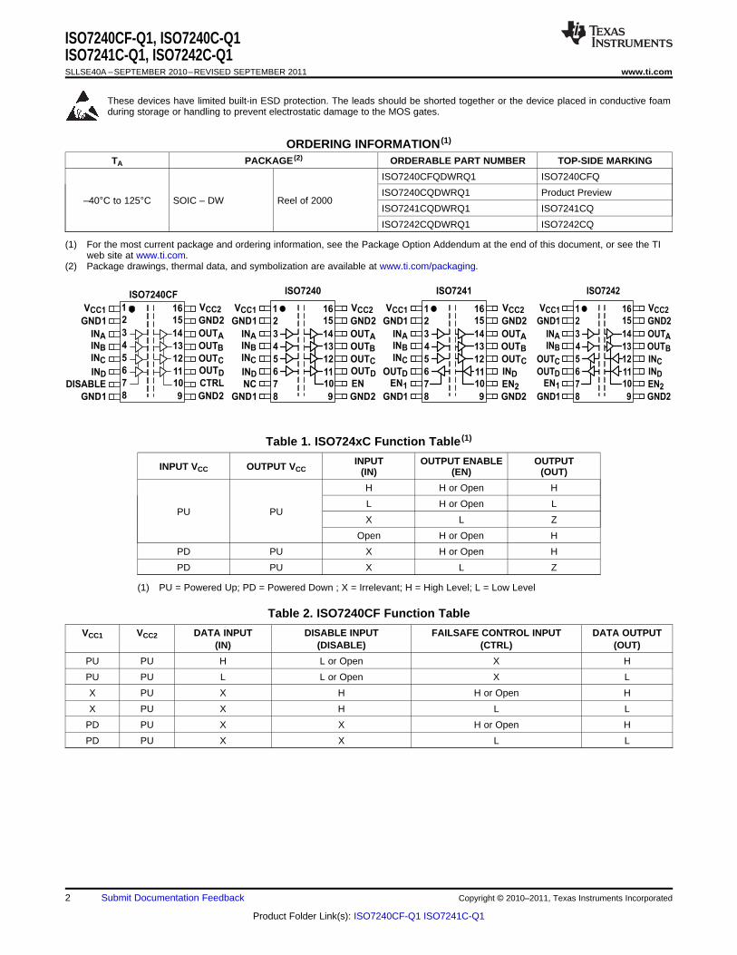
ISO7240CF-Q1, ISO7240C-Q1ISO7241C-Q1, ISO7242C-Q1SLLSE40A –SEPTEMBER 2010–REVISED SEPTEMBER 2011 www.ti.com
These devices have limited built-in ESD protection. The leads should be shorted together or the device placed in conductive foamduring storage or handling to prevent electrostatic damage to the MOS gates.
ORDERING INFORMATION (1)
TA PACKAGE (2) ORDERABLE PART NUMBER TOP-SIDE MARKING
ISO7240CFQDWRQ1 ISO7240CFQ
ISO7240CQDWRQ1 Product Preview–40°C to 125°C SOIC – DW Reel of 2000
ISO7241CQDWRQ1 ISO7241CQ
ISO7242CQDWRQ1 ISO7242CQ
(1) For the most current package and ordering information, see the Package Option Addendum at the end of this document, or see the TIweb site at www.ti.com.
(2) Package drawings, thermal data, and symbolization are available at www.ti.com/packaging.
Table 1. ISO724xC Function Table (1)
INPUT OUTPUT ENABLE OUTPUTINPUT VCC OUTPUT VCC (IN) (EN) (OUT)
H H or Open H
L H or Open LPU PU
X L Z
Open H or Open H
PD PU X H or Open H
PD PU X L Z
(1) PU = Powered Up; PD = Powered Down ; X = Irrelevant; H = High Level; L = Low Level
Table 2. ISO7240CF Function Table
VCC1 VCC2 DATA INPUT DISABLE INPUT FAILSAFE CONTROL INPUT DATA OUTPUT(IN) (DISABLE) (CTRL) (OUT)
PU PU H L or Open X H
PU PU L L or Open X L
X PU X H H or Open H
X PU X H L L
PD PU X X H or Open H
PD PU X X L L
2 Submit Documentation Feedback Copyright © 2010–2011, Texas Instruments Incorporated
Product Folder Link(s): ISO7240CF-Q1 ISO7241C-Q1
ISO7240CF-Q1, ISO7240C-Q1ISO7241C-Q1, ISO7242C-Q1
www.ti.com SLLSE40A –SEPTEMBER 2010–REVISED SEPTEMBER 2011
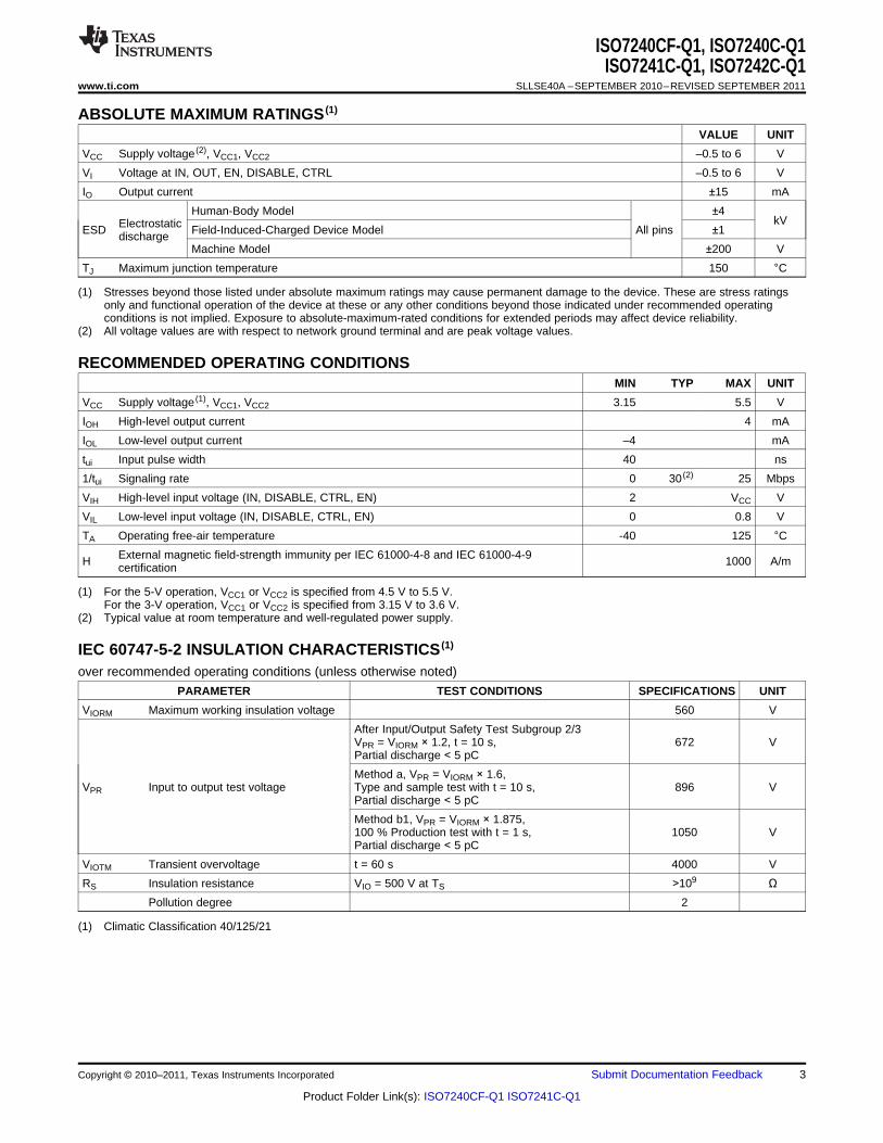
ABSOLUTE MAXIMUM RATINGS (1)
VALUE UNIT
VCC Supply voltage (2), VCC1, VCC2 –0.5 to 6 V
VI Voltage at IN, OUT, EN, DISABLE, CTRL –0.5 to 6 V
IO Output current ±15 mA
Human-Body Model ±4kVElectrostaticESD Field-Induced-Charged Device Model All pins ±1discharge
Machine Model ±200 V
TJ Maximum junction temperature 150 °C
(1) Stresses beyond those listed under absolute maximum ratings may cause permanent damage to the device. These are stress ratingsonly and functional operation of the device at these or any other conditions beyond those indicated under recommended operatingconditions is not implied. Exposure to absolute-maximum-rated conditions for extended periods may affect device reliability.
(2) All voltage values are with respect to network ground terminal and are peak voltage values.
RECOMMENDED OPERATING CONDITIONSMIN TYP MAX UNIT
VCC Supply voltage (1), VCC1, VCC2 3.15 5.5 V
IOH High-level output current 4 mA
IOL Low-level output current –4 mA
tui Input pulse width 40 ns
1/tui Signaling rate 0 30 (2) 25 Mbps
VIH High-level input voltage (IN, DISABLE, CTRL, EN) 2 VCC V
VIL Low-level input voltage (IN, DISABLE, CTRL, EN) 0 0.8 V
TA Operating free-air temperature -40 125 °CExternal magnetic field-strength immunity per IEC 61000-4-8 and IEC 61000-4-9H 1000 A/mcertification
(1) For the 5-V operation, VCC1 or VCC2 is specified from 4.5 V to 5.5 V.For the 3-V operation, VCC1 or VCC2 is specified from 3.15 V to 3.6 V.
(2) Typical value at room temperature and well-regulated power supply.
IEC 60747-5-2 INSULATION CHARACTERISTICS (1)
over recommended operating conditions (unless otherwise noted)
PARAMETER TEST CONDITIONS SPECIFICATIONS UNIT
VIORM Maximum working insulation voltage 560 V
After Input/Output Safety Test Subgroup 2/3VPR = VIORM × 1.2, t = 10 s, 672 VPartial discharge < 5 pC
Method a, VPR = VIORM × 1.6,VPR Input to output test voltage Type and sample test with t = 10 s, 896 V
Partial discharge < 5 pC
Method b1, VPR = VIORM × 1.875,100 % Production test with t = 1 s, 1050 VPartial discharge < 5 pC
VIOTM Transient overvoltage t = 60 s 4000 V
RS Insulation resistance VIO = 500 V at TS >109 ΩPollution degree 2
(1) Climatic Classification 40/125/21
Copyright © 2010–2011, Texas Instruments Incorporated Submit Documentation Feedback 3
Product Folder Link(s): ISO7240CF-Q1 ISO7241C-Q1
ISO7240CF-Q1, ISO7240C-Q1ISO7241C-Q1, ISO7242C-Q1SLLSE40A –SEPTEMBER 2010–REVISED SEPTEMBER 2011 www.ti.com
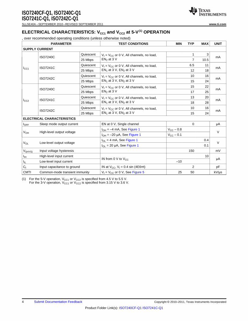
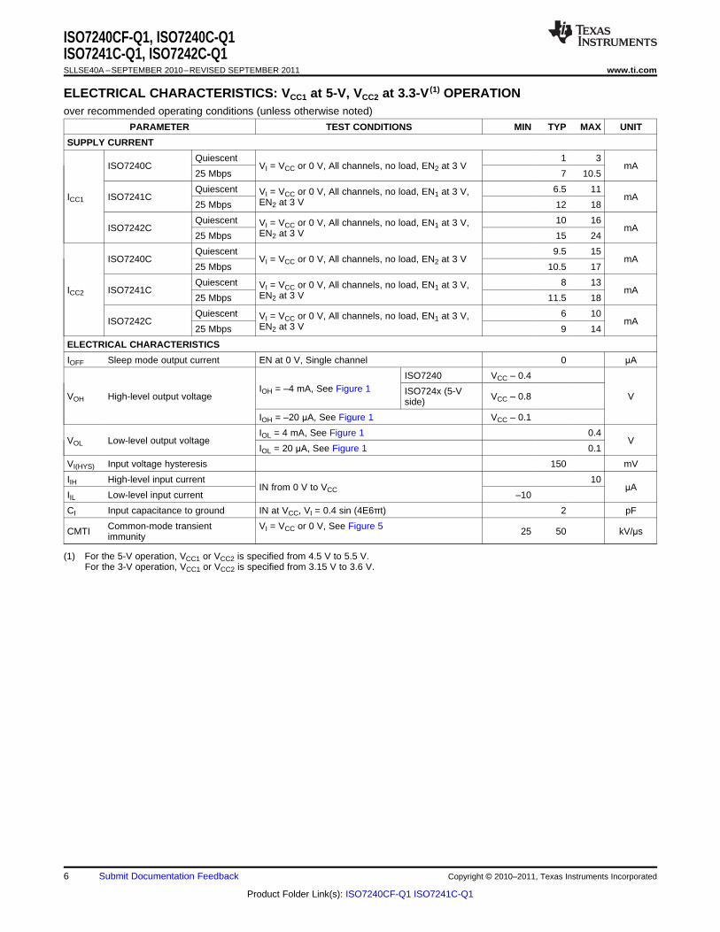
ELECTRICAL CHARACTERISTICS: VCC1 and VCC2 at 5-V (1) OPERATION, over recommended operating conditions (unless otherwise noted)
PARAMETER TEST CONDITIONS MIN TYP MAX UNIT
SUPPLY CURRENT
Quiescent 1 3VI = VCC or 0 V, All channels, no load,ISO7240C mA
EN2 at 3 V25 Mbps 7 10.5
Quiescent 6.5 11VI = VCC or 0 V, All channels, no load,ICC1 ISO7241C mA
EN1 at 3 V, EN2 at 3 V25 Mbps 12 18
Quiescent 10 16VI = VCC or 0 V, All channels, no load,ISO7242C mA
EN1 at 3 V, EN2 at 3 V25 Mbps 15 24
Quiescent 15 22VI = VCC or 0 V, All channels, no load,ISO7240C mA
EN2 at 3 V25 Mbps 17 25
Quiescent 13 20VI = VCC or 0 V, All channels, no load,ICC2 ISO7241C mA
EN1 at 3 V, EN2 at 3 V25 Mbps 18 28
Quiescent 10 16VI = VCC or 0 V, All channels, no load,ISO7242C mA
EN1 at 3 V, EN2 at 3 V25 Mbps 15 24
ELECTRICAL CHARACTERISTICS
IOFF Sleep mode output current EN at 0 V, Single channel 0 μA
IOH = –4 mA, See Figure 1 VCC – 0.8VOH High-level output voltage V
IOH = –20 μA, See Figure 1 VCC – 0.1
IOL = 4 mA, See Figure 1 0.4VOL Low-level output voltage V
IOL = 20 μA, See Figure 1 0.1
VI(HYS) Input voltage hysteresis 150 mV
IIH High-level input current 10IN from 0 V to VCC μA
IIL Low-level input current –10
CI Input capacitance to ground IN at VCC, VI = 0.4 sin (4E6πt) 2 pF
CMTI Common-mode transient immunity VI = VCC or 0 V, See Figure 5 25 50 kV/μs
(1) For the 5-V operation, VCC1 or VCC2 is specified from 4.5 V to 5.5 V.For the 3-V operation, VCC1 or VCC2 is specified from 3.15 V to 3.6 V.
4 Submit Documentation Feedback Copyright © 2010–2011, Texas Instruments Incorporated
Product Folder Link(s): ISO7240CF-Q1 ISO7241C-Q1
ISO7240CF-Q1, ISO7240C-Q1ISO7241C-Q1, ISO7242C-Q1
www.ti.com SLLSE40A –SEPTEMBER 2010–REVISED SEPTEMBER 2011
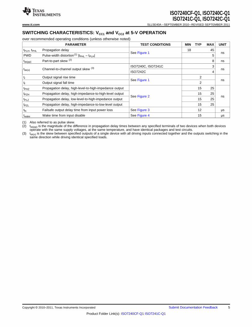
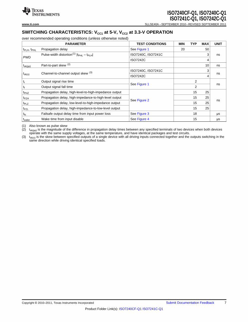
SWITCHING CHARACTERISTICS: VCC1 and VCC2 at 5-V OPERATIONover recommended operating conditions (unless otherwise noted)
PARAMETER TEST CONDITIONS MIN TYP MAX UNIT
tPLH, tPHL Propagation delay 18 45See Figure 1 ns
PWD Pulse-width distortion (1) |tPHL – tPLH| 5
tsk(pp) Part-to-part skew (2) 8 ns
ISO7240C, ISO7241C 3tsk(o) Channel-to-channel output skew (3) ns
ISO7242C 4
tr Output signal rise time 2See Figure 1 ns
tf Output signal fall time 2
tPHZ Propagation delay, high-level-to-high-impedance output 15 25
tPZH Propagation delay, high-impedance-to-high-level output 15 25See Figure 2 ns
tPLZ Propagation delay, low-level-to-high-impedance output 15 25
tPZL Propagation delay, high-impedance-to-low-level output 15 25
tfs Failsafe output delay time from input power loss See Figure 3 12 μs
twake Wake time from input disable See Figure 4 15 μs
(1) Also referred to as pulse skew.(2) tsk(pp) is the magnitude of the difference in propagation delay times between any specified terminals of two devices when both devices
operate with the same supply voltages, at the same temperature, and have identical packages and test circuits.(3) tsk(o) is the skew between specified outputs of a single device with all driving inputs connected together and the outputs switching in the
same direction while driving identical specified loads.
Copyright © 2010–2011, Texas Instruments Incorporated Submit Documentation Feedback 5
Product Folder Link(s): ISO7240CF-Q1 ISO7241C-Q1
ISO7240CF-Q1, ISO7240C-Q1ISO7241C-Q1, ISO7242C-Q1SLLSE40A –SEPTEMBER 2010–REVISED SEPTEMBER 2011 www.ti.com
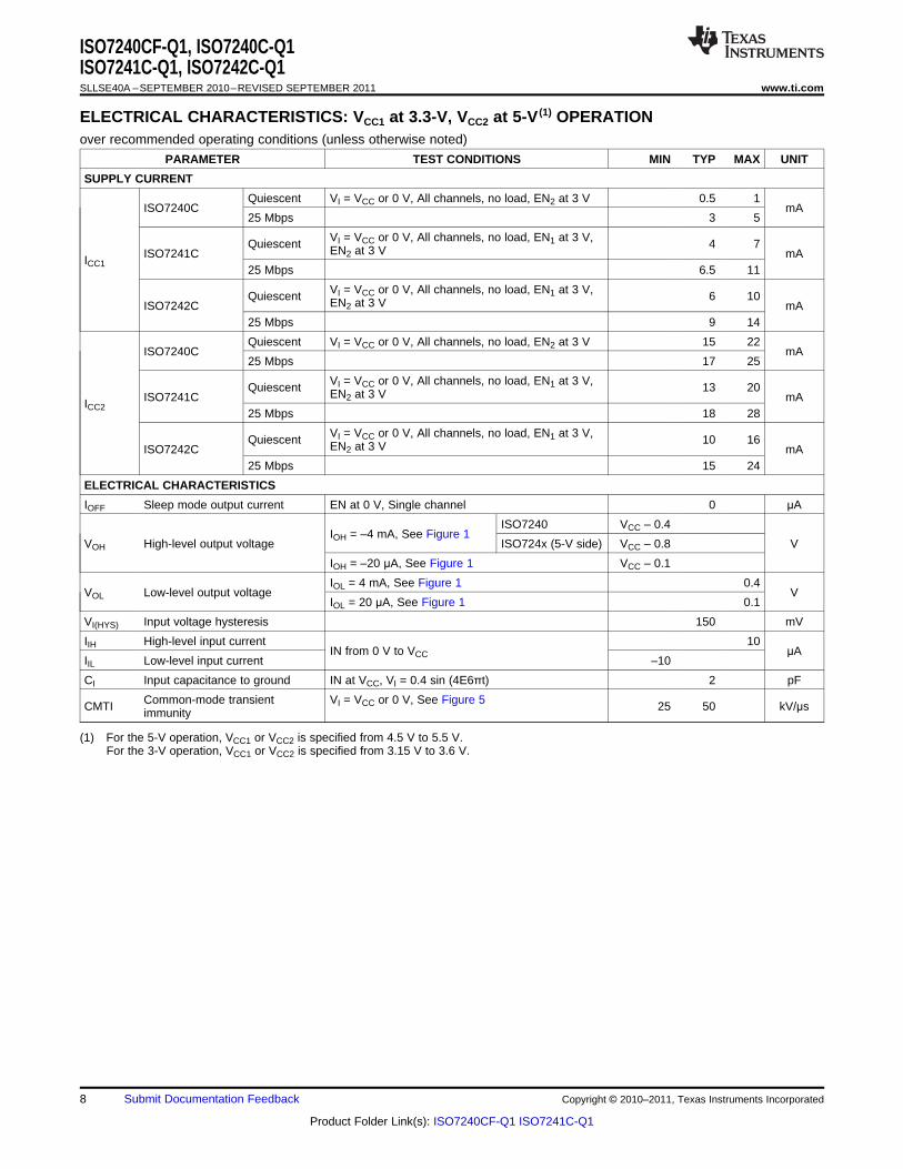
ELECTRICAL CHARACTERISTICS: VCC1 at 5-V, VCC2 at 3.3-V (1) OPERATIONover recommended operating conditions (unless otherwise noted)
PARAMETER TEST CONDITIONS MIN TYP MAX UNIT
SUPPLY CURRENT
Quiescent 1 3ISO7240C VI = VCC or 0 V, All channels, no load, EN2 at 3 V mA
25 Mbps 7 10.5
Quiescent 6.5 11VI = VCC or 0 V, All channels, no load, EN1 at 3 V,ICC1 ISO7241C mAEN2 at 3 V25 Mbps 12 18
Quiescent 10 16VI = VCC or 0 V, All channels, no load, EN1 at 3 V,ISO7242C mAEN2 at 3 V25 Mbps 15 24
Quiescent 9.5 15ISO7240C VI = VCC or 0 V, All channels, no load, EN2 at 3 V mA
25 Mbps 10.5 17
Quiescent 8 13VI = VCC or 0 V, All channels, no load, EN1 at 3 V,ICC2 ISO7241C mAEN2 at 3 V25 Mbps 11.5 18
Quiescent 6 10VI = VCC or 0 V, All channels, no load, EN1 at 3 V,ISO7242C mAEN2 at 3 V25 Mbps 9 14
ELECTRICAL CHARACTERISTICS
IOFF Sleep mode output current EN at 0 V, Single channel 0 μA
ISO7240 VCC – 0.4IOH = –4 mA, See Figure 1 ISO724x (5-VVOH High-level output voltage VCC – 0.8 Vside)
IOH = –20 μA, See Figure 1 VCC – 0.1
IOL = 4 mA, See Figure 1 0.4VOL Low-level output voltage V
IOL = 20 μA, See Figure 1 0.1
VI(HYS) Input voltage hysteresis 150 mV
IIH High-level input current 10IN from 0 V to VCC μA
IIL Low-level input current –10
CI Input capacitance to ground IN at VCC, VI = 0.4 sin (4E6πt) 2 pF
Common-mode transient VI = VCC or 0 V, See Figure 5CMTI 25 50 kV/μsimmunity
(1) For the 5-V operation, VCC1 or VCC2 is specified from 4.5 V to 5.5 V.For the 3-V operation, VCC1 or VCC2 is specified from 3.15 V to 3.6 V.
6 Submit Documentation Feedback Copyright © 2010–2011, Texas Instruments Incorporated
Product Folder Link(s): ISO7240CF-Q1 ISO7241C-Q1
ISO7240CF-Q1, ISO7240C-Q1ISO7241C-Q1, ISO7242C-Q1
www.ti.com SLLSE40A –SEPTEMBER 2010–REVISED SEPTEMBER 2011
SWITCHING CHARACTERISTICS: VCC1 at 5-V, VCC2 at 3.3-V OPERATIONover recommended operating conditions (unless otherwise noted)
PARAMETER TEST CONDITIONS MIN TYP MAX UNIT
tPLH, tPHL Propagation delay See Figure 1 20 50
Pulse-width distortion (1) |tPHL – tPLH| ISO7240C, ISO7241C 3 nsPWD
ISO7242C 4
tsk(pp) Part-to-part skew (2) 10 ns
ISO7240C, ISO7241C 3tsk(o) Channel-to-channel output skew (3) ns
ISO7242C 4
tr Output signal rise time 2See Figure 1 ns
tf Output signal fall time 2
tPHZ Propagation delay, high-level-to-high-impedance output 15 25
tPZH Propagation delay, high-impedance-to-high-level output 15 25See Figure 2 ns
tPLZ Propagation delay, low-level-to-high-impedance output 15 25
tPZL Propagation delay, high-impedance-to-low-level output 15 25
tfs Failsafe output delay time from input power loss See Figure 3 18 μs
twake Wake time from input disable See Figure 4 15 μs
(1) Also known as pulse skew(2) tsk(pp) is the magnitude of the difference in propagation delay times between any specified terminals of two devices when both devices
operate with the same supply voltages, at the same temperature, and have identical packages and test circuits.(3) tsk(o) is the skew between specified outputs of a single device with all driving inputs connected together and the outputs switching in the
same direction while driving identical specified loads.
Copyright © 2010–2011, Texas Instruments Incorporated Submit Documentation Feedback 7
Product Folder Link(s): ISO7240CF-Q1 ISO7241C-Q1
ISO7240CF-Q1, ISO7240C-Q1ISO7241C-Q1, ISO7242C-Q1SLLSE40A –SEPTEMBER 2010–REVISED SEPTEMBER 2011 www.ti.com
ELECTRICAL CHARACTERISTICS: VCC1 at 3.3-V, VCC2 at 5-V (1) OPERATIONover recommended operating conditions (unless otherwise noted)
PARAMETER TEST CONDITIONS MIN TYP MAX UNIT
SUPPLY CURRENT
Quiescent VI = VCC or 0 V, All channels, no load, EN2 at 3 V 0.5 1ISO7240C mA
25 Mbps 3 5
VI = VCC or 0 V, All channels, no load, EN1 at 3 V,Quiescent 4 7EN2 at 3 VISO7241C mAICC125 Mbps 6.5 11
VI = VCC or 0 V, All channels, no load, EN1 at 3 V,Quiescent 6 10EN2 at 3 VISO7242C mA25 Mbps 9 14
Quiescent VI = VCC or 0 V, All channels, no load, EN2 at 3 V 15 22ISO7240C mA
25 Mbps 17 25
VI = VCC or 0 V, All channels, no load, EN1 at 3 V,Quiescent 13 20EN2 at 3 VISO7241C mAICC225 Mbps 18 28
VI = VCC or 0 V, All channels, no load, EN1 at 3 V,Quiescent 10 16EN2 at 3 VISO7242C mA25 Mbps 15 24
ELECTRICAL CHARACTERISTICS
IOFF Sleep mode output current EN at 0 V, Single channel 0 μA
ISO7240 VCC – 0.4IOH = –4 mA, See Figure 1
VOH High-level output voltage ISO724x (5-V side) VCC – 0.8 V
IOH = –20 μA, See Figure 1 VCC – 0.1
IOL = 4 mA, See Figure 1 0.4VOL Low-level output voltage V
IOL = 20 μA, See Figure 1 0.1
VI(HYS) Input voltage hysteresis 150 mV
IIH High-level input current 10IN from 0 V to VCC μA
IIL Low-level input current –10
CI Input capacitance to ground IN at VCC, VI = 0.4 sin (4E6πt) 2 pF
Common-mode transient VI = VCC or 0 V, See Figure 5CMTI 25 50 kV/μsimmunity
(1) For the 5-V operation, VCC1 or VCC2 is specified from 4.5 V to 5.5 V.For the 3-V operation, VCC1 or VCC2 is specified from 3.15 V to 3.6 V.
8 Submit Documentation Feedback Copyright © 2010–2011, Texas Instruments Incorporated
Product Folder Link(s): ISO7240CF-Q1 ISO7241C-Q1
ISO7240CF-Q1, ISO7240C-Q1ISO7241C-Q1, ISO7242C-Q1
www.ti.com SLLSE40A –SEPTEMBER 2010–REVISED SEPTEMBER 2011
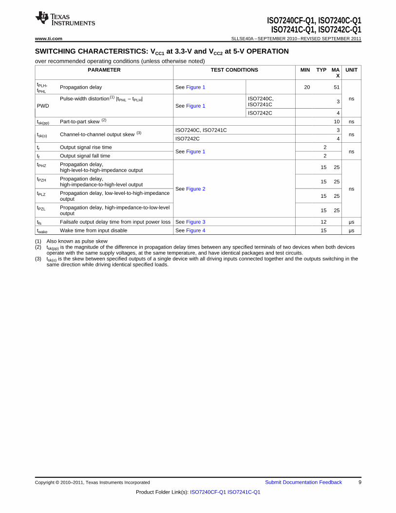
SWITCHING CHARACTERISTICS: VCC1 at 3.3-V and VCC2 at 5-V OPERATIONover recommended operating conditions (unless otherwise noted)
PARAMETER TEST CONDITIONS MIN TYP MA UNITX
tPLH, Propagation delay See Figure 1 20 51tPHL
Pulse-width distortion (1) |tPHL – tPLH| ISO7240C, ns3ISO7241CPWD See Figure 1ISO7242C 4
tsk(pp) Part-to-part skew (2) 10 ns
ISO7240C, ISO7241C 3tsk(o) Channel-to-channel output skew (3) ns
ISO7242C 4
tr Output signal rise time 2See Figure 1 ns
tf Output signal fall time 2
tPHZ Propagation delay, 15 25high-level-to-high-impedance output
tPZH Propagation delay, 15 25high-impedance-to-high-level outputSee Figure 2 ns
tPLZ Propagation delay, low-level-to-high-impedance 15 25output
tPZL Propagation delay, high-impedance-to-low-level 15 25output
tfs Failsafe output delay time from input power loss See Figure 3 12 μs
twake Wake time from input disable See Figure 4 15 μs
(1) Also known as pulse skew(2) tsk(pp) is the magnitude of the difference in propagation delay times between any specified terminals of two devices when both devices
operate with the same supply voltages, at the same temperature, and have identical packages and test circuits.(3) tsk(o) is the skew between specified outputs of a single device with all driving inputs connected together and the outputs switching in the
same direction while driving identical specified loads.
Copyright © 2010–2011, Texas Instruments Incorporated Submit Documentation Feedback 9
Product Folder Link(s): ISO7240CF-Q1 ISO7241C-Q1
ISO7240CF-Q1, ISO7240C-Q1ISO7241C-Q1, ISO7242C-Q1SLLSE40A –SEPTEMBER 2010–REVISED SEPTEMBER 2011 www.ti.com
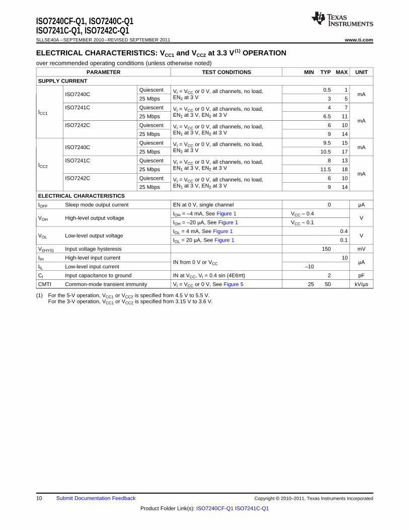
ELECTRICAL CHARACTERISTICS: VCC1 and VCC2 at 3.3 V (1) OPERATIONover recommended operating conditions (unless otherwise noted)
PARAMETER TEST CONDITIONS MIN TYP MAX UNIT
SUPPLY CURRENT
Quiescent 0.5 1VI = VCC or 0 V, all channels, no load,ISO7240C mAEN2 at 3 V25 Mbps 3 5
ISO7241C Quiescent 4 7VI = VCC or 0 V, all channels, no load,ICC1 EN1 at 3 V, EN2 at 3 V25 Mbps 6.5 11mA
ISO7242C Quiescent 6 10VI = VCC or 0 V, all channels, no load,EN1 at 3 V, EN2 at 3 V25 Mbps 9 14
Quiescent 9.5 15VI = VCC or 0 V, all channels, no load,ISO7240C mAEN2 at 3 V25 Mbps 10.5 17
ISO7241C Quiescent 8 13VI = VCC or 0 V, all channels, no load,ICC2 EN1 at 3 V, EN2 at 3 V25 Mbps 11.5 18mA
ISO7242C Quiescent 6 10VI = VCC or 0 V, all channels, no load,EN1 at 3 V, EN2 at 3 V25 Mbps 9 14
ELECTRICAL CHARACTERISTICS
IOFF Sleep mode output current EN at 0 V, single channel 0 μA
IOH = –4 mA, See Figure 1 VCC – 0.4VOH High-level output voltage V
IOH = –20 μA, See Figure 1 VCC – 0.1
IOL = 4 mA, See Figure 1 0.4VOL Low-level output voltage V
IOL = 20 μA, See Figure 1 0.1
VI(HYS) Input voltage hysteresis 150 mV
IIH High-level input current 10IN from 0 V or VCC μA
IIL Low-level input current –10
CI Input capacitance to ground IN at VCC, VI = 0.4 sin (4E6πt) 2 pF
CMTI Common-mode transient immunity VI = VCC or 0 V, See Figure 5 25 50 kV/μs
(1) For the 5-V operation, VCC1 or VCC2 is specified from 4.5 V to 5.5 V.For the 3-V operation, VCC1 or VCC2 is specified from 3.15 V to 3.6 V.
10 Submit Documentation Feedback Copyright © 2010–2011, Texas Instruments Incorporated
Product Folder Link(s): ISO7240CF-Q1 ISO7241C-Q1
ISO7240CF-Q1, ISO7240C-Q1ISO7241C-Q1, ISO7242C-Q1
www.ti.com SLLSE40A –SEPTEMBER 2010–REVISED SEPTEMBER 2011
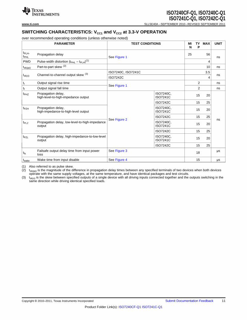
SWITCHING CHARACTERISTICS: VCC1 and VCC2 at 3.3-V OPERATIONover recommended operating conditions (unless otherwise noted)
PARAMETER TEST CONDITIONS MI TY MAX UNITN P
tPLH, Propagation delay 25 56tPHL See Figure 1 nsPWD Pulse-width distortion |tPHL – tPLH| (1) 4
tsk(pp) Part-to-part skew (2) 10 ns
ISO7240C, ISO7241C 3.5tsk(o) Channel-to-channel output skew (3) ns
ISO7242C 4
tr Output signal rise time 2 nsSee Figure 1
tf Output signal fall time 2 ns
tPHZ Propagation delay, ISO7240C, 15 20high-level-to-high-impedance output ISO7241C
ISO7242C 15 25
tPZH Propagation delay, ISO7240C, 15 20high-impedance-to-high-level output ISO7241C
ISO7242C 15 25See Figure 2 ns
tPLZ Propagation delay, low-level-to-high-impedance ISO7240C, 15 20output ISO7241C
ISO7242C 15 25
tPZL Propagation delay, high-impedance-to-low-level ISO7240C, 15 20output ISO7241C
ISO7242C 15 25
Failsafe output delay time from input power See Figure 3 μstfs 18loss
twake Wake time from input disable See Figure 4 15 μs
(1) Also referred to as pulse skew.(2) tsk(pp) is the magnitude of the difference in propagation delay times between any specified terminals of two devices when both devices
operate with the same supply voltages, at the same temperature, and have identical packages and test circuits.(3) tsk(o) is the skew between specified outputs of a single device with all driving inputs connected together and the outputs switching in the
same direction while driving identical specified loads.
Copyright © 2010–2011, Texas Instruments Incorporated Submit Documentation Feedback 11
Product Folder Link(s): ISO7240CF-Q1 ISO7241C-Q1
IN OUT
VOCL
Input
Generator 50 WVI
NOTE A NOTE B
V 1/2CC
t ft r
10%
90%50%
0 V
50%
VI
tPLH tPHL
VOH
VOL
ISO
LA
TIO
N B
AR
RIE
R
VO
V 1/2CC
V 1CC
Input
Generator 50 W
OUT
EN
VO
VI
IN0V
ISO
LA
TIO
NB
AR
RIE
R
CL
NOTE A
NOTE
B
Vcc
Input
Generator
OUT
R = 1 k ±1%L W
EN
VO
VI
IN3V
ISO
LA
TIO
NB
AR
RIE
R
CL
NOTE A
NOTE
B 0 V
0 V
VI
50% 0.5 V
tPHZ
tPZH
VO
VCC
0 VtPLZ
t
VO
VI
0.5 V
VOL
50%
PZL
R = 1 k ±1%L W
50 W
VCC/2
VOH
VCC/2
VCC/2
VCC
VCC/2
VCC
ISO7240CF-Q1, ISO7240C-Q1ISO7241C-Q1, ISO7242C-Q1SLLSE40A –SEPTEMBER 2010–REVISED SEPTEMBER 2011 www.ti.com
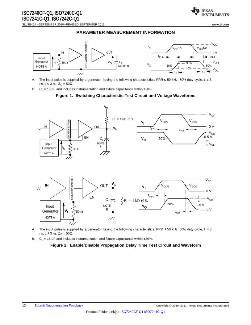
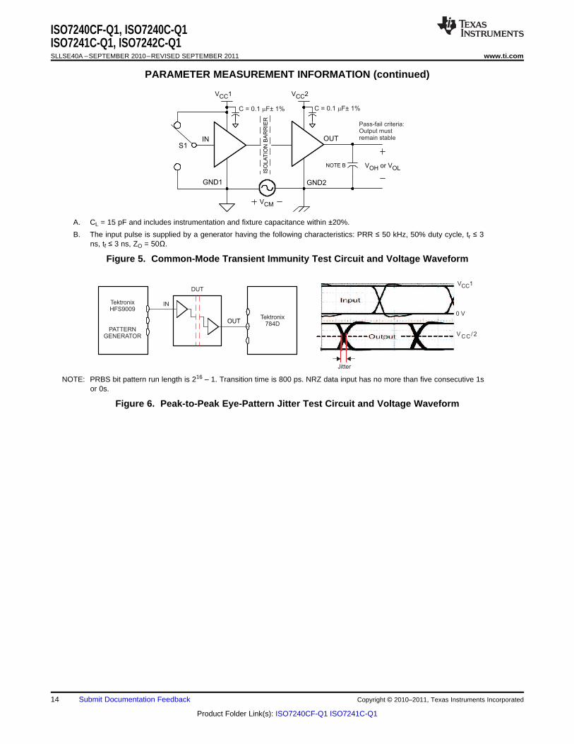
PARAMETER MEASUREMENT INFORMATION
A. The input pulse is supplied by a generator having the following characteristics: PRR ≤ 50 kHz, 50% duty cycle, tr ≤ 3ns, tf ≤ 3 ns, ZO = 50Ω.
B. CL = 15 pF and includes instrumentation and fixture capacitance within ±20%.
Figure 1. Switching Characteristic Test Circuit and Voltage Waveforms
A. The input pulse is supplied by a generator having the following characteristics: PRR ≤ 50 kHz, 50% duty cycle, tr ≤ 3ns, tf ≤ 3 ns, ZO = 50Ω.
B. CL = 15 pF and includes instrumentation and fixture capacitance within ±20%.
Figure 2. Enable/Disable Propagation Delay Time Test Circuit and Waveform
12 Submit Documentation Feedback Copyright © 2010–2011, Texas Instruments Incorporated
Product Folder Link(s): ISO7240CF-Q1 ISO7241C-Q1
tfs
IN OUT
ISO
LA
TIO
N B
AR
RIE
R
0 V
or
V 1CC
VCC
VI
CL
NOTE A
VO
VI
VO 50%
VCC
0 V
VOH
VOL
2.7 V
fs low
VO
Input
Generator 50 W
OUT
DISABLE
VI
IN0V
VO
VI
50 %
50 %
twake
VO
Input
Generator50 W
OUT
DISABLE
VO
VI
IN
0 V
C L
waket
(Note A)
(Note A )
C L
(Note B)
(Note B )
VCC2
0 V
0 V
0 V
0 V
VI
CTRL
3 V
CTRL
3 V
ISO
LA
TIO
N B
AR
RIE
RIS
OL
AT
ION
BA
RR
IER
VCC
VCC
V /2CC2
VCC2
V /2CC2
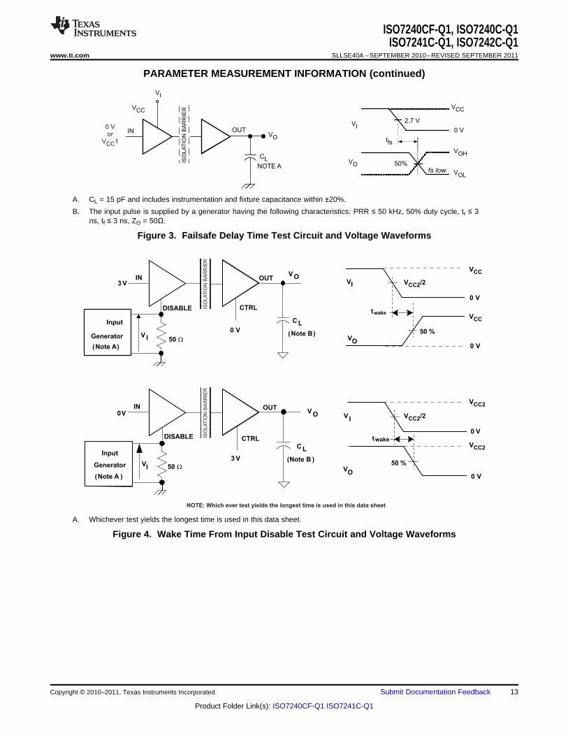
NOTE: Which ever test yields the longest time is used in this data sheet
ISO7240CF-Q1, ISO7240C-Q1ISO7241C-Q1, ISO7242C-Q1
www.ti.com SLLSE40A –SEPTEMBER 2010–REVISED SEPTEMBER 2011
PARAMETER MEASUREMENT INFORMATION (continued)
A. CL = 15 pF and includes instrumentation and fixture capacitance within ±20%.
B. The input pulse is supplied by a generator having the following characteristics: PRR ≤ 50 kHz, 50% duty cycle, tr ≤ 3ns, tf ≤ 3 ns, ZO = 50Ω.
Figure 3. Failsafe Delay Time Test Circuit and Voltage Waveforms
A. Whichever test yields the longest time is used in this data sheet.
Figure 4. Wake Time From Input Disable Test Circuit and Voltage Waveforms
Copyright © 2010–2011, Texas Instruments Incorporated Submit Documentation Feedback 13
Product Folder Link(s): ISO7240CF-Q1 ISO7241C-Q1
VCM
IN OUT
GND1
NOTE B
S1
V or VOH OL
ISO
LA
TIO
N B
AR
RIE
R
V 1CC V 2CC
C = 0.1 F± 1%m C = 0.1 F± 1%m
GND2
Pass-fail criteria:Output mustremain stable
OUT
Tektronix
HFS9009
PATTERN
GENERATOR
IN
DUT
Tektronix
784D
V 1CC
0 V
V /2C C
Jitter
ISO7240CF-Q1, ISO7240C-Q1ISO7241C-Q1, ISO7242C-Q1SLLSE40A –SEPTEMBER 2010–REVISED SEPTEMBER 2011 www.ti.com
PARAMETER MEASUREMENT INFORMATION (continued)
A. CL = 15 pF and includes instrumentation and fixture capacitance within ±20%.
B. The input pulse is supplied by a generator having the following characteristics: PRR ≤ 50 kHz, 50% duty cycle, tr ≤ 3ns, tf ≤ 3 ns, ZO = 50Ω.
Figure 5. Common-Mode Transient Immunity Test Circuit and Voltage Waveform
NOTE: PRBS bit pattern run length is 216 – 1. Transition time is 800 ps. NRZ data input has no more than five consecutive 1sor 0s.
Figure 6. Peak-to-Peak Eye-Pattern Jitter Test Circuit and Voltage Waveform
14 Submit Documentation Feedback Copyright © 2010–2011, Texas Instruments Incorporated
Product Folder Link(s): ISO7240CF-Q1 ISO7241C-Q1
ISO7240CF-Q1, ISO7240C-Q1ISO7241C-Q1, ISO7242C-Q1
www.ti.com SLLSE40A –SEPTEMBER 2010–REVISED SEPTEMBER 2011
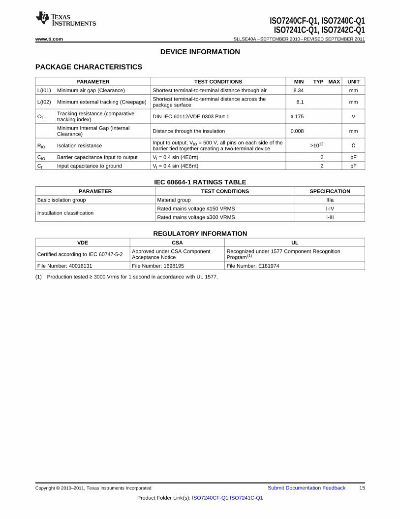
DEVICE INFORMATION
PACKAGE CHARACTERISTICS
PARAMETER TEST CONDITIONS MIN TYP MAX UNIT
L(I01) Minimum air gap (Clearance) Shortest terminal-to-terminal distance through air 8.34 mm
Shortest terminal-to-terminal distance across theL(I02) Minimum external tracking (Creepage) 8.1 mmpackage surface
Tracking resistance (comparativeCTI DIN IEC 60112/VDE 0303 Part 1 ≥ 175 Vtracking index)
Minimum Internal Gap (Internal Distance through the insulation 0.008 mmClearance)
Input to output, VIO = 500 V, all pins on each side of theRIO Isolation resistance >1012 Ωbarrier tied together creating a two-terminal device
CIO Barrier capacitance Input to output VI = 0.4 sin (4E6πt) 2 pF
CI Input capacitance to ground VI = 0.4 sin (4E6πt) 2 pF
IEC 60664-1 RATINGS TABLEPARAMETER TEST CONDITIONS SPECIFICATION
Basic isolation group Material group IIIa
Rated mains voltage ≤150 VRMS I-IVInstallation classification
Rated mains voltage ≤300 VRMS I-III
REGULATORY INFORMATIONVDE CSA UL
Approved under CSA Component Recognized under 1577 Component RecognitionCertified according to IEC 60747-5-2 Acceptance Notice Program (1)
File Number: 40016131 File Number: 1698195 File Number: E181974
(1) Production tested ≥ 3000 Vrms for 1 second in accordance with UL 1577.
Copyright © 2010–2011, Texas Instruments Incorporated Submit Documentation Feedback 15
Product Folder Link(s): ISO7240CF-Q1 ISO7241C-Q1
OUT
8 W
13 W
VCC
Output
IN
VCCVCC
ISO7240CF
Input
1 MW
VCC
500 W
VCC
EN
Enable
500 W
VCC
1 MW
IN
VCCVCCVCC
Input
1 MW
500 W
ISO7240CF-Q1, ISO7240C-Q1ISO7241C-Q1, ISO7242C-Q1SLLSE40A –SEPTEMBER 2010–REVISED SEPTEMBER 2011 www.ti.com
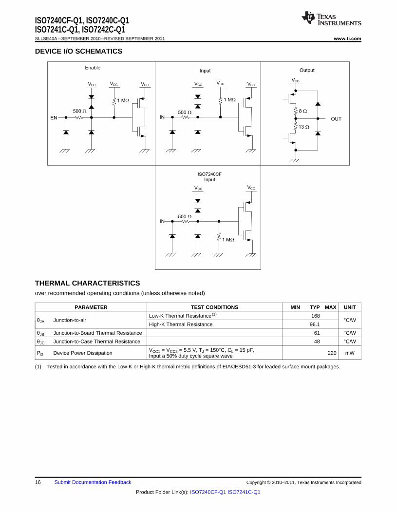
DEVICE I/O SCHEMATICS
THERMAL CHARACTERISTICSover recommended operating conditions (unless otherwise noted)
PARAMETER TEST CONDITIONS MIN TYP MAX UNIT
Low-K Thermal Resistance (1) 168θJA Junction-to-air °C/W
High-K Thermal Resistance 96.1
θJB Junction-to-Board Thermal Resistance 61 °C/W
θJC Junction-to-Case Thermal Resistance 48 °C/W
VCC1 = VCC2 = 5.5 V, TJ = 150°C, CL = 15 pF,PD Device Power Dissipation 220 mWInput a 50% duty cycle square wave
(1) Tested in accordance with the Low-K or High-K thermal metric definitions of EIA/JESD51-3 for leaded surface mount packages.
16 Submit Documentation Feedback Copyright © 2010–2011, Texas Instruments Incorporated
Product Folder Link(s): ISO7240CF-Q1 ISO7241C-Q1
0
5
10
15
20
25
30
35
0 25 50 75 100 125 150
Signaling Rate - Mbps
I-
Su
pp
ly C
urr
en
t -
mA
/RM
SC
C
40
45
T = 25°C,
Load = 15 pF,All Channels
A
5-V ICC2
3.3-V ICC2
3.3-V ICC1
5-V ICC1
0
5
10
15
20
25
30
35
40
45
0 25 50 75 100 125 150
Signaling Rate - Mbps
I-
Su
pp
ly C
urr
en
t -
mA
/RM
SC
C
T = 25°C,
Load = 15 pF,All Channels
A
5-V ICC2
3.3-V ICC2
3.3-V ICC1
5-V ICC1
0
5
10
15
20
25
30
35
40
45
0 25 50 75 100 125 150
Signaling Rate - Mbps
I-
Su
pp
ly C
urr
en
t -
mA
/RM
SC
C
T = 25°C,
Load = 15 pF,All Channels
A
5-V ICC1,ICC2
3.3-V ICC1,ICC2
0
5
10
15
20
25
30
35
40
45
-40 -25 -10 5 20 35 50 65 80 95 110 125
T - Free-Air Temperature - CA °
Pro
pag
ati
on
Dela
y -
ns
T = 25°C,
Load = 15 pF,All Channels
A
C 3.3-V , tpHLtpLH
M 3.3-V , tpHLtpLH
C 5-V , tpHLtpLH
M 5-V , tpHLtpLH
ISO7240CF-Q1, ISO7240C-Q1ISO7241C-Q1, ISO7242C-Q1
www.ti.com SLLSE40A –SEPTEMBER 2010–REVISED SEPTEMBER 2011
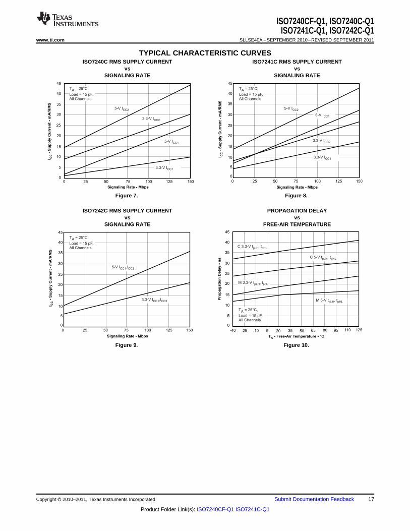
TYPICAL CHARACTERISTIC CURVESISO7240C RMS SUPPLY CURRENT ISO7241C RMS SUPPLY CURRENT
vs vsSIGNALING RATE SIGNALING RATE
Figure 7. Figure 8.
ISO7242C RMS SUPPLY CURRENT PROPAGATION DELAYvs vs
SIGNALING RATE FREE-AIR TEMPERATURE
Figure 9. Figure 10.
Copyright © 2010–2011, Texas Instruments Incorporated Submit Documentation Feedback 17
Product Folder Link(s): ISO7240CF-Q1 ISO7241C-Q1
1
1.05
1.1
1.15
1.2
1.25
1.3
1.35
1.4
-40 -25 -10 5 20 35 50 65 80 95 110 125
Inp
ut
Vo
ltag
e T
hre
sh
old
- V
T - Free-Air Temperature - CA °
5 V Vth+
3.3 V Vth+
5 V Vth-
3.3 V Vth-
Air Flow at 7 cf/m,Low_K Board
2
2.1
2.2
2.3
2.4
2.5
2.6
2.7
2.8
2.9
3
-40 -25 -10 5 20 35 50 65 80 95 110 125
T - Free-Air Temperature - CA °
VF
ailsafe
Th
resh
old
- V
CC
1-
Vfs+
Vfs-
V at 5 V or 3.3 V,
Load = 15 pF,Air Flow at 7/cf/m,Low-K Board
CC
0
5
10
15
20
25
30
35
40
45
50
0 1 2 3 4 5
I-
Ou
tpu
t C
urr
en
t -
mA
O
V - Output Voltage - VO
V = 5 VCC
V = 3.3 VCC
Load = 15 pF,
T = 25 CA °
0
10
20
30
40
50
0 2 4 6
I-
Ou
tpu
t C
urr
en
t -
mA
O
V - Output Voltage - VO
V = 5 VCC
V = 3.3 VCC
Load = 15 pF,
T = 25 CA °
ISO7240CF-Q1, ISO7240C-Q1ISO7241C-Q1, ISO7242C-Q1SLLSE40A –SEPTEMBER 2010–REVISED SEPTEMBER 2011 www.ti.com
TYPICAL CHARACTERISTIC CURVES (continued)INPUT VOLTAGE THRESHOLD VCC1 FAILSAFE THRESHOLD
vs vsFREE-AIR TEMPERATURE FREE-AIR TEMPERATURE
Figure 11. Figure 12.
HIGH-LEVEL OUTPUT CURRENT LOW-LEVEL OUTPUT CURRENTvs vs
HIGH-LEVEL OUTPUT VOLTAGE LOW-LEVEL OUTPUT VOLTAGE
Figure 13. Figure 14.
18 Submit Documentation Feedback Copyright © 2010–2011, Texas Instruments Incorporated
Product Folder Link(s): ISO7240CF-Q1 ISO7241C-Q1
1
2
3
4
5
6
7
8
ISO7240x
9
10
11
12
13
14
15
16
NC
INA
GND1
GND1
GND2
GND2
INB
INC
OUT A
OUT C
OUT B
IND OUT D
EN
0.1 Fm
VCC1
2 mm
max. from
VCC1
2 mm
max. from
VCC2
VCC2
0.1 Fm
1
2
3
4
5
6
7
8
ISO7240CF
9
10
11
12
13
14
15
16
DISABLE
INA
GND1
GND1
GND2
GND2
INB
INC
OUT A
OUT C
OUT B
IND OUT D
CTRL
0.1 Fm
VCC1
2 mm
max. from
VCC1
2 mm
max. from
VCC2
VCC2
0.1 Fm
ISO7240CF-Q1, ISO7240C-Q1ISO7241C-Q1, ISO7242C-Q1
www.ti.com SLLSE40A –SEPTEMBER 2010–REVISED SEPTEMBER 2011
APPLICATION INFORMATION
Figure 15. Typical ISO7240x Application Circuit
Figure 16. Typical ISO7240CF Failsafe-Low Application Circuit
Copyright © 2010–2011, Texas Instruments Incorporated Submit Documentation Feedback 19
Product Folder Link(s): ISO7240CF-Q1 ISO7241C-Q1
10
100
0 250 500 750 1000
WORKING VOLTAGE (VIORM) -- V
WO
RK
ING
LIF
E -
-Y
EA
RS
VIORM at 560-V
28 Years
880120
ISO7240CF-Q1, ISO7240C-Q1ISO7241C-Q1, ISO7242C-Q1SLLSE40A –SEPTEMBER 2010–REVISED SEPTEMBER 2011 www.ti.com
LIFE EXPECTANCY vs WORKING VOLTAGE
Figure 17. Time-Dependant Dielectric Breakdown Testing Results
20 Submit Documentation Feedback Copyright © 2010–2011, Texas Instruments Incorporated
Product Folder Link(s): ISO7240CF-Q1 ISO7241C-Q1
PACKAGE OPTION ADDENDUM
www.ti.com 11-Apr-2013
Addendum-Page 1
PACKAGING INFORMATION
Orderable Device Status(1)
Package Type PackageDrawing
Pins PackageQty
Eco Plan(2)
Lead/Ball Finish MSL Peak Temp(3)
Op Temp (°C) Top-Side Markings(4)
Samples
ISO7240CFQDWRQ1 ACTIVE SOIC DW 16 2000 Green (RoHS& no Sb/Br)
CU NIPDAU Level-3-260C-168 HR -40 to 125 ISO7240CFQ
ISO7241CQDWRQ1 ACTIVE SOIC DW 16 2000 Green (RoHS& no Sb/Br)
CU NIPDAU Level-3-260C-168 HR -40 to 125 ISO7241CQ
ISO7242CQDWRQ1 ACTIVE SOIC DW 16 2000 Green (RoHS& no Sb/Br)
CU NIPDAU Level-3-260C-168 HR -40 to 125 ISO7242CQ
(1) The marketing status values are defined as follows:ACTIVE: Product device recommended for new designs.LIFEBUY: TI has announced that the device will be discontinued, and a lifetime-buy period is in effect.NRND: Not recommended for new designs. Device is in production to support existing customers, but TI does not recommend using this part in a new design.PREVIEW: Device has been announced but is not in production. Samples may or may not be available.OBSOLETE: TI has discontinued the production of the device.
(2) Eco Plan - The planned eco-friendly classification: Pb-Free (RoHS), Pb-Free (RoHS Exempt), or Green (RoHS & no Sb/Br) - please check http://www.ti.com/productcontent for the latest availabilityinformation and additional product content details.TBD: The Pb-Free/Green conversion plan has not been defined.Pb-Free (RoHS): TI's terms "Lead-Free" or "Pb-Free" mean semiconductor products that are compatible with the current RoHS requirements for all 6 substances, including the requirement thatlead not exceed 0.1% by weight in homogeneous materials. Where designed to be soldered at high temperatures, TI Pb-Free products are suitable for use in specified lead-free processes.Pb-Free (RoHS Exempt): This component has a RoHS exemption for either 1) lead-based flip-chip solder bumps used between the die and package, or 2) lead-based die adhesive used betweenthe die and leadframe. The component is otherwise considered Pb-Free (RoHS compatible) as defined above.Green (RoHS & no Sb/Br): TI defines "Green" to mean Pb-Free (RoHS compatible), and free of Bromine (Br) and Antimony (Sb) based flame retardants (Br or Sb do not exceed 0.1% by weightin homogeneous material)
(3) MSL, Peak Temp. -- The Moisture Sensitivity Level rating according to the JEDEC industry standard classifications, and peak solder temperature.
(4) Multiple Top-Side Markings will be inside parentheses. Only one Top-Side Marking contained in parentheses and separated by a "~" will appear on a device. If a line is indented then it is acontinuation of the previous line and the two combined represent the entire Top-Side Marking for that device.
Important Information and Disclaimer:The information provided on this page represents TI's knowledge and belief as of the date that it is provided. TI bases its knowledge and belief on informationprovided by third parties, and makes no representation or warranty as to the accuracy of such information. Efforts are underway to better integrate information from third parties. TI has taken andcontinues to take reasonable steps to provide representative and accurate information but may not have conducted destructive testing or chemical analysis on incoming materials and chemicals.TI and TI suppliers consider certain information to be proprietary, and thus CAS numbers and other limited information may not be available for release.
In no event shall TI's liability arising out of such information exceed the total purchase price of the TI part(s) at issue in this document sold by TI to Customer on an annual basis.
PACKAGE OPTION ADDENDUM
www.ti.com 11-Apr-2013
Addendum-Page 2
OTHER QUALIFIED VERSIONS OF ISO7240CF-Q1, ISO7241C-Q1, ISO7242C-Q1 :
• Catalog: ISO7240CF, ISO7241C, ISO7242C
NOTE: Qualified Version Definitions:
• Catalog - TI's standard catalog product
TAPE AND REEL INFORMATION
*All dimensions are nominal
Device PackageType
PackageDrawing
Pins SPQ ReelDiameter
(mm)
ReelWidth
W1 (mm)
A0(mm)
B0(mm)
K0(mm)
P1(mm)
W(mm)
Pin1Quadrant
ISO7240CFQDWRQ1 SOIC DW 16 2000 330.0 16.4 10.75 10.7 2.7 12.0 16.0 Q1
ISO7241CQDWRQ1 SOIC DW 16 2000 330.0 16.4 10.75 10.7 2.7 12.0 16.0 Q1
ISO7242CQDWRQ1 SOIC DW 16 2000 330.0 16.4 10.75 10.7 2.7 12.0 16.0 Q1
PACKAGE MATERIALS INFORMATION
www.ti.com 15-Aug-2013
Pack Materials-Page 1
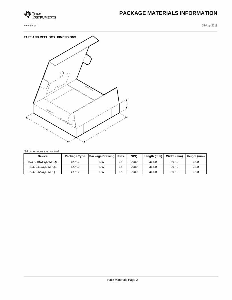
*All dimensions are nominal
Device Package Type Package Drawing Pins SPQ Length (mm) Width (mm) Height (mm)
ISO7240CFQDWRQ1 SOIC DW 16 2000 367.0 367.0 38.0
ISO7241CQDWRQ1 SOIC DW 16 2000 367.0 367.0 38.0
ISO7242CQDWRQ1 SOIC DW 16 2000 367.0 367.0 38.0
PACKAGE MATERIALS INFORMATION
www.ti.com 15-Aug-2013
Pack Materials-Page 2
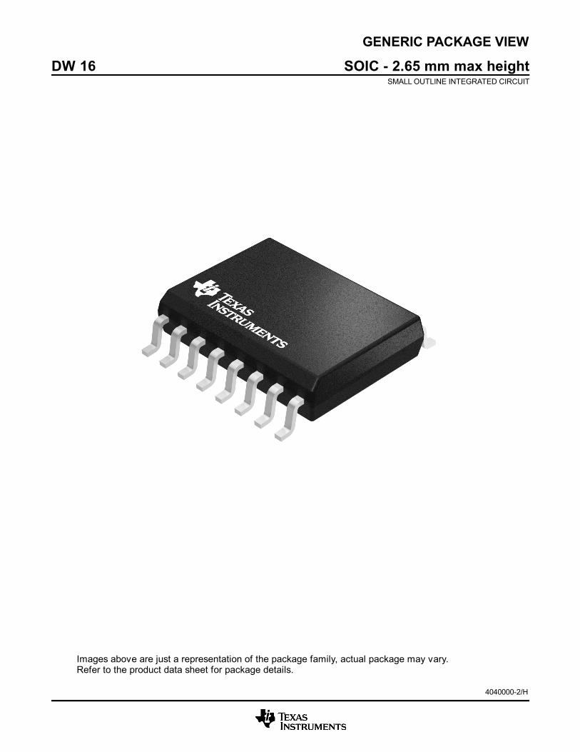
GENERIC PACKAGE VIEW
Images above are just a representation of the package family, actual package may vary.Refer to the product data sheet for package details.
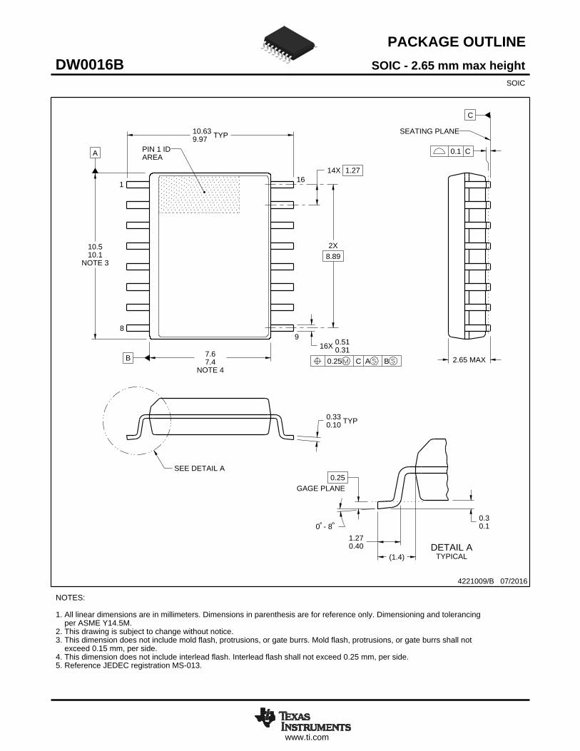
DW 16 SOIC - 2.65 mm max heightSMALL OUTLINE INTEGRATED CIRCUIT
4040000-2/H
www.ti.com
PACKAGE OUTLINE
C
TYP10.639.97
2.65 MAX
14X 1.27
16X 0.510.31
2X8.89
TYP0.330.10
0 - 80.30.1
(1.4)
0.25GAGE PLANE
1.270.40
A
NOTE 3
10.510.1
BNOTE 4
7.67.4
4221009/B 07/2016
SOIC - 2.65 mm max heightDW0016BSOIC
NOTES: 1. All linear dimensions are in millimeters. Dimensions in parenthesis are for reference only. Dimensioning and tolerancing per ASME Y14.5M. 2. This drawing is subject to change without notice. 3. This dimension does not include mold flash, protrusions, or gate burrs. Mold flash, protrusions, or gate burrs shall not exceed 0.15 mm, per side. 4. This dimension does not include interlead flash. Interlead flash shall not exceed 0.25 mm, per side.5. Reference JEDEC registration MS-013.
1 16
0.25 C A B
98
PIN 1 IDAREA
SEATING PLANE
0.1 C
SEE DETAIL A
DETAIL ATYPICAL
SCALE 1.500
www.ti.com
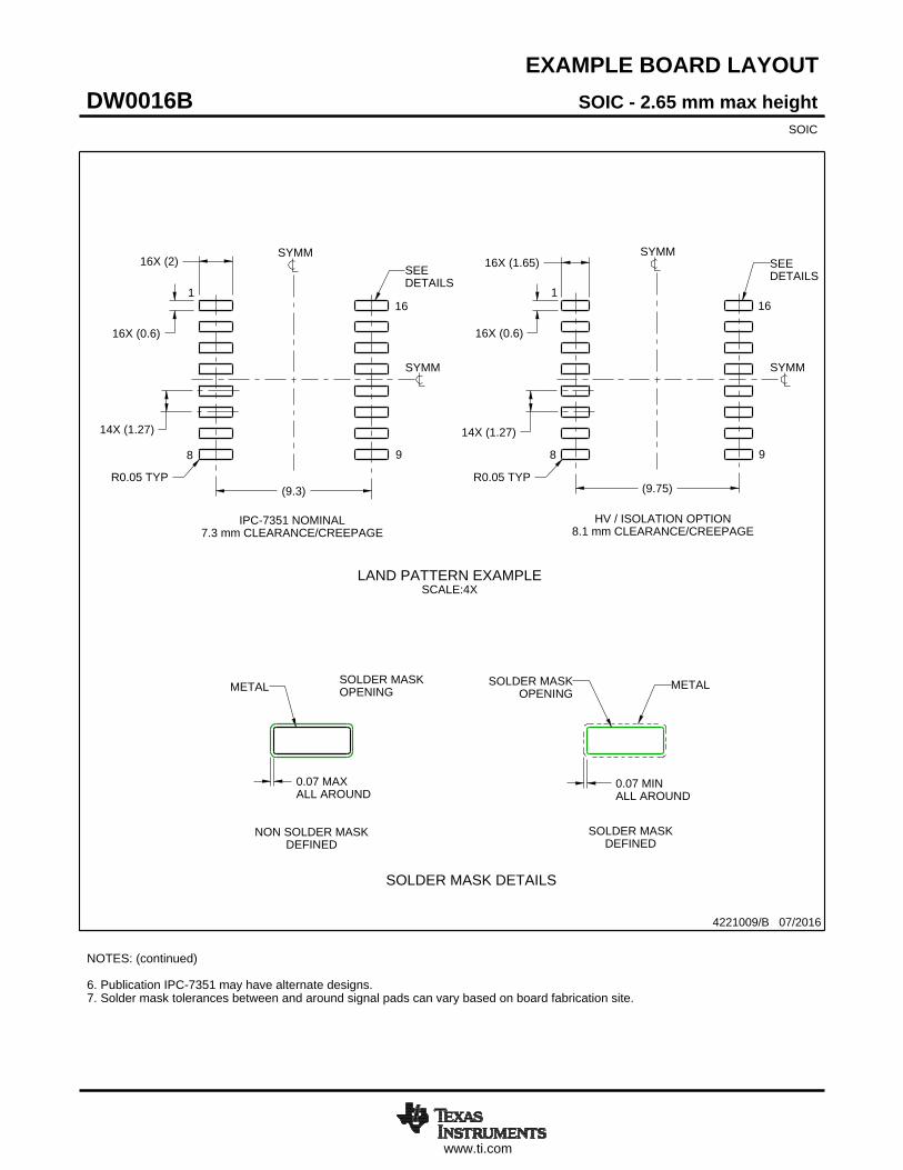
EXAMPLE BOARD LAYOUT
(9.75)R0.05 TYP
0.07 MAXALL AROUND
0.07 MINALL AROUND
(9.3)
14X (1.27)
R0.05 TYP
16X (1.65)
16X (0.6)
14X (1.27)
16X (2)
16X (0.6)
4221009/B 07/2016
SOIC - 2.65 mm max heightDW0016BSOIC
SYMM
SYMM
SEEDETAILS
1
8 9
16
SYMM
HV / ISOLATION OPTION8.1 mm CLEARANCE/CREEPAGE
NOTES: (continued) 6. Publication IPC-7351 may have alternate designs. 7. Solder mask tolerances between and around signal pads can vary based on board fabrication site.
METAL SOLDER MASKOPENING
NON SOLDER MASKDEFINED
SOLDER MASK DETAILS
OPENINGSOLDER MASK METAL
SOLDER MASKDEFINED
LAND PATTERN EXAMPLESCALE:4X
SYMM
1
8 9
16
IPC-7351 NOMINAL7.3 mm CLEARANCE/CREEPAGE
SEEDETAILS
www.ti.com
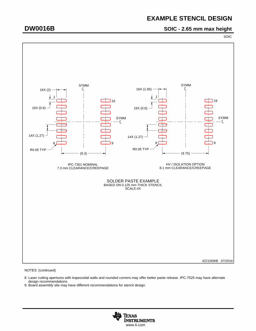
EXAMPLE STENCIL DESIGN
R0.05 TYPR0.05 TYP
16X (1.65)
16X (0.6)
14X (1.27)
(9.75)
16X (2)
16X (0.6)
14X (1.27)
(9.3)
4221009/B 07/2016
SOIC - 2.65 mm max heightDW0016BSOIC
NOTES: (continued) 8. Laser cutting apertures with trapezoidal walls and rounded corners may offer better paste release. IPC-7525 may have alternate design recommendations. 9. Board assembly site may have different recommendations for stencil design.
SYMM
SYMM
1
8 9
16
HV / ISOLATION OPTION8.1 mm CLEARANCE/CREEPAGE
SOLDER PASTE EXAMPLEBASED ON 0.125 mm THICK STENCIL
SCALE:4X
SYMM
SYMM
1
8 9
16
IPC-7351 NOMINAL7.3 mm CLEARANCE/CREEPAGE
IMPORTANT NOTICE
Texas Instruments Incorporated (TI) reserves the right to make corrections, enhancements, improvements and other changes to itssemiconductor products and services per JESD46, latest issue, and to discontinue any product or service per JESD48, latest issue. Buyersshould obtain the latest relevant information before placing orders and should verify that such information is current and complete.TI’s published terms of sale for semiconductor products (http://www.ti.com/sc/docs/stdterms.htm) apply to the sale of packaged integratedcircuit products that TI has qualified and released to market. Additional terms may apply to the use or sale of other types of TI products andservices.Reproduction of significant portions of TI information in TI data sheets is permissible only if reproduction is without alteration and isaccompanied by all associated warranties, conditions, limitations, and notices. TI is not responsible or liable for such reproduceddocumentation. Information of third parties may be subject to additional restrictions. Resale of TI products or services with statementsdifferent from or beyond the parameters stated by TI for that product or service voids all express and any implied warranties for theassociated TI product or service and is an unfair and deceptive business practice. TI is not responsible or liable for any such statements.Buyers and others who are developing systems that incorporate TI products (collectively, “Designers”) understand and agree that Designersremain responsible for using their independent analysis, evaluation and judgment in designing their applications and that Designers havefull and exclusive responsibility to assure the safety of Designers' applications and compliance of their applications (and of all TI productsused in or for Designers’ applications) with all applicable regulations, laws and other applicable requirements. Designer represents that, withrespect to their applications, Designer has all the necessary expertise to create and implement safeguards that (1) anticipate dangerousconsequences of failures, (2) monitor failures and their consequences, and (3) lessen the likelihood of failures that might cause harm andtake appropriate actions. Designer agrees that prior to using or distributing any applications that include TI products, Designer willthoroughly test such applications and the functionality of such TI products as used in such applications.TI’s provision of technical, application or other design advice, quality characterization, reliability data or other services or information,including, but not limited to, reference designs and materials relating to evaluation modules, (collectively, “TI Resources”) are intended toassist designers who are developing applications that incorporate TI products; by downloading, accessing or using TI Resources in anyway, Designer (individually or, if Designer is acting on behalf of a company, Designer’s company) agrees to use any particular TI Resourcesolely for this purpose and subject to the terms of this Notice.TI’s provision of TI Resources does not expand or otherwise alter TI’s applicable published warranties or warranty disclaimers for TIproducts, and no additional obligations or liabilities arise from TI providing such TI Resources. TI reserves the right to make corrections,enhancements, improvements and other changes to its TI Resources. TI has not conducted any testing other than that specificallydescribed in the published documentation for a particular TI Resource.Designer is authorized to use, copy and modify any individual TI Resource only in connection with the development of applications thatinclude the TI product(s) identified in such TI Resource. NO OTHER LICENSE, EXPRESS OR IMPLIED, BY ESTOPPEL OR OTHERWISETO ANY OTHER TI INTELLECTUAL PROPERTY RIGHT, AND NO LICENSE TO ANY TECHNOLOGY OR INTELLECTUAL PROPERTYRIGHT OF TI OR ANY THIRD PARTY IS GRANTED HEREIN, including but not limited to any patent right, copyright, mask work right, orother intellectual property right relating to any combination, machine, or process in which TI products or services are used. Informationregarding or referencing third-party products or services does not constitute a license to use such products or services, or a warranty orendorsement thereof. Use of TI Resources may require a license from a third party under the patents or other intellectual property of thethird party, or a license from TI under the patents or other intellectual property of TI.TI RESOURCES ARE PROVIDED “AS IS” AND WITH ALL FAULTS. TI DISCLAIMS ALL OTHER WARRANTIES ORREPRESENTATIONS, EXPRESS OR IMPLIED, REGARDING RESOURCES OR USE THEREOF, INCLUDING BUT NOT LIMITED TOACCURACY OR COMPLETENESS, TITLE, ANY EPIDEMIC FAILURE WARRANTY AND ANY IMPLIED WARRANTIES OFMERCHANTABILITY, FITNESS FOR A PARTICULAR PURPOSE, AND NON-INFRINGEMENT OF ANY THIRD PARTY INTELLECTUALPROPERTY RIGHTS. TI SHALL NOT BE LIABLE FOR AND SHALL NOT DEFEND OR INDEMNIFY DESIGNER AGAINST ANY CLAIM,INCLUDING BUT NOT LIMITED TO ANY INFRINGEMENT CLAIM THAT RELATES TO OR IS BASED ON ANY COMBINATION OFPRODUCTS EVEN IF DESCRIBED IN TI RESOURCES OR OTHERWISE. IN NO EVENT SHALL TI BE LIABLE FOR ANY ACTUAL,DIRECT, SPECIAL, COLLATERAL, INDIRECT, PUNITIVE, INCIDENTAL, CONSEQUENTIAL OR EXEMPLARY DAMAGES INCONNECTION WITH OR ARISING OUT OF TI RESOURCES OR USE THEREOF, AND REGARDLESS OF WHETHER TI HAS BEENADVISED OF THE POSSIBILITY OF SUCH DAMAGES.Unless TI has explicitly designated an individual product as meeting the requirements of a particular industry standard (e.g., ISO/TS 16949and ISO 26262), TI is not responsible for any failure to meet such industry standard requirements.Where TI specifically promotes products as facilitating functional safety or as compliant with industry functional safety standards, suchproducts are intended to help enable customers to design and create their own applications that meet applicable functional safety standardsand requirements. Using products in an application does not by itself establish any safety features in the application. Designers mustensure compliance with safety-related requirements and standards applicable to their applications. Designer may not use any TI products inlife-critical medical equipment unless authorized officers of the parties have executed a special contract specifically governing such use.Life-critical medical equipment is medical equipment where failure of such equipment would cause serious bodily injury or death (e.g., lifesupport, pacemakers, defibrillators, heart pumps, neurostimulators, and implantables). Such equipment includes, without limitation, allmedical devices identified by the U.S. Food and Drug Administration as Class III devices and equivalent classifications outside the U.S.TI may expressly designate certain products as completing a particular qualification (e.g., Q100, Military Grade, or Enhanced Product).Designers agree that it has the necessary expertise to select the product with the appropriate qualification designation for their applicationsand that proper product selection is at Designers’ own risk. Designers are solely responsible for compliance with all legal and regulatoryrequirements in connection with such selection.Designer will fully indemnify TI and its representatives against any damages, costs, losses, and/or liabilities arising out of Designer’s non-compliance with the terms and provisions of this Notice.
Mailing Address: Texas Instruments, Post Office Box 655303, Dallas, Texas 75265Copyright © 2017, Texas Instruments Incorporated