Embed Size (px)
Citation preview

Edition 3.0
July. 20171
Ku-Band Power Amplifier MMIC
SMM5085V1B
FEATURES
・High Output Power: Pout=33.0dBm (typ.)
・Linear Gain: GL=25.0dB (typ.)
・Frequency Band: 12.7 to 15.4GHz
・Impedance Matched Zin/Zout=50ohm
・Integrated Power Detector
・Small Hermetic Metal-Ceramic SMT Package(V1B)
DESCRIPTION
The SMM5085V1B is a MMIC amplifier that contains a three-
stages amplifier, internally matched, for standard communications
band in the 12.7 to 15.4GHz frequency range.
Sumitomo Electric’s stringent Quality Assurance Program assures
the highest reliability and consistent performance.
ABSOLUTE MAXIMUM RATING
Item Symbol Rating Unit
Drain-Source Voltage VDD 10 V
Gate-Source Voltage VGG -3 V
Input Power Pin +23 dBm
Storage Temperature Tstg -55 to +125 deg.C
RECOMMENDED OPERATING CONDITIONS
Item Symbol Recommend Unit
Drain-Source Voltage VDD Up to +6 V
Input Power Pin Up to +16 dBm
Operating Case Temperature Tc -40 to +85 deg.C
ELECTRICAL CHARACTERISTICS (Case Temperature Tc=25deg.C)
Item Symbol Test Conditions Limits Unit
Min. Typ. Max.
RF Frequency Range f VDD=6.0V 12.7 - 15.4 GHz
Gate Bias Voltage VGG IDD(DC)=1200mA typ. -0.50 -0.1 -0.04 V
Output Power at Pin=13dBm POUT 31.5 33.0 - dBm
Output Power at 1dB G.C.P. P1dB VGG-constant - 32.5 - dBm
Power Gain at 1dB G.C.P. G1dB ZS=ZL=50ohm 20 24 - dB
Power-added Efficiency at 1dB G.C.P. PAE - 20 - %
Third Order Intermodulation Distortion *1 IM3 *1:Df=+10MHz -38 -44 - dBc
Drain Current at 1dB G.C.P. IDDRF Pout=20dBm (S.C.L.) - 1500 1800 mA
Input Return Loss (at Pin=-20dBm) RLIN - 8 - dB
Output Return Loss (at Pin=-20dBm) RLOUT - 8 - dB
G.C.P. :Gain Compression Point, S.C.L. :Single Carrier Level
ESD Class 0B up to 250V
Note : Based on JEDEC JESD22-A114-C (C=100pF, R=1.5kohm)
CASE STYLE V1B
RoHS COMLIANCE YES
Ordering Information
Part Number Order Unit Packing
SMM5085V1B No Limitation 48pcs. / Tray x4 Trays = 192pcs. / Packing
SMM5085V1BT 500pcs. 500pcs. / Reel x1 Reel = 500pcs. / Packing

Edition 3.0
July. 20172
Ku-Band Power Amplifier MMIC
SMM5085V1B
-80
-70
-60
-50
-40
-30
-20
14 16 18 20 22 24 26 28
Inte
r-m
od
ula
tio
n D
isto
rtio
n (d
Bc)
Output Power (dBm) (S.C.L.)
12.7GHz 13.5GHz 14.5GHz 15.4GHz
800
1000
1200
1400
1600
1800
2000
2200
2400
2600
2800
16
18
20
22
24
26
28
30
32
34
36
-10 -8 -6 -4 -2 0 2 4 6 8 10 12 14 16
Dra
in C
urr
en
t (m
A)
Ou
tpu
t P
ow
er
(dB
m)
Input Power (dBm)
12.7GHz 13.5GHz 14.5GHz 15.4GHz
Output Power, Drain Current vs. Input Power
VDD=6V, IDD(DC)=1200mA
Output Power vs. Frequency
VDD=6V, IDD(DC)=1200mA
IMD Performance vs. Output Power
VDD=6V, IDD(DC)=1200mA
16
18
20
22
24
26
28
30
32
34
36
12 13 14 15 16O
utp
ut
Po
wer
(dB
m)
Frequency (GHz)
Pin=4dBm 0dBm 4dBm
8dBm 13dBm P1dB
IM3
IM5
IDD
Pout
Edition 3.0
July. 20173
Ku-Band Power Amplifier MMIC
SMM5085V1B
800
1000
1200
1400
1600
1800
2000
2200
2400
2600
2800
16
18
20
22
24
26
28
30
32
34
36
-10 -8 -6 -4 -2 0 2 4 6 8 10 12 14 16
Dra
in C
urr
en
t (m
A)
Ou
tpu
t P
ow
er
(dB
m)
Input Power (dBm)
VDD=4V VDD=5V VDD=6V
800
1000
1200
1400
1600
1800
2000
2200
2400
2600
2800
16
18
20
22
24
26
28
30
32
34
36
-10 -8 -6 -4 -2 0 2 4 6 8 10 12 14 16
Dra
in C
urr
en
t (m
A)
Ou
tpu
t P
ow
er
(dB
m)
Input Power (dBm)
VDD=4V VDD=5V VDD=6V
800
1000
1200
1400
1600
1800
2000
2200
2400
2600
2800
16
18
20
22
24
26
28
30
32
34
36
-10 -8 -6 -4 -2 0 2 4 6 8 10 12 14 16
Dra
in C
urr
en
t (m
A)
Ou
tpu
t P
ow
er
(dB
m)
Input Power (dBm)
VDD=4V VDD=5V VDD=6V
800
1000
1200
1400
1600
1800
2000
2200
2400
2600
2800
16
18
20
22
24
26
28
30
32
34
36
-10 -8 -6 -4 -2 0 2 4 6 8 10 12 14 16
Dra
in C
urr
en
t (m
A)
Ou
tpu
t P
ow
er
(dB
m)
Input Power (dBm)
VDD=4V VDD=5V VDD=6V
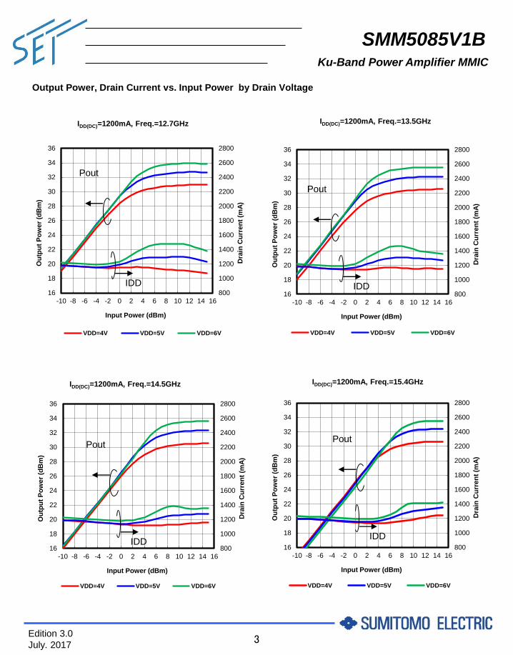
Output Power, Drain Current vs. Input Power by Drain Voltage
IDD(DC)=1200mA, Freq.=13.5GHzIDD(DC)=1200mA, Freq.=12.7GHz
IDD(DC)=1200mA, Freq.=15.4GHzIDD(DC)=1200mA, Freq.=14.5GHz
IDD
Pout
IDD
Pout
IDD
Pout
IDD
Pout

Edition 3.0
July. 20174
Ku-Band Power Amplifier MMIC
SMM5085V1B
Output Power, Drain Current vs. Input Power by Drain Current
VDD=6V, Freq.=12.7GHz VDD=6V, Freq.=13.5GHz
VDD=6V, Freq.=14.5GHz VDD=6V, Freq.=15.4GHz
700
900
1100
1300
1500
1700
1900
2100
2300
2500
2700
16
18
20
22
24
26
28
30
32
34
36
-10 -8 -6 -4 -2 0 2 4 6 8 10 12 14 16
Dra
in C
urr
en
t (m
A)
Ou
tpu
t P
ow
er
(dB
m)
Input Power (dBm)
IDD=800mA IDD=1000mA
IDD=1200mA IDD=1400mA
700
900
1100
1300
1500
1700
1900
2100
2300
2500
2700
16
18
20
22
24
26
28
30
32
34
36
-10 -8 -6 -4 -2 0 2 4 6 8 10 12 14 16
Dra
in C
urr
en
t (m
A)
Ou
tpu
t P
ow
er
(dB
m)
Input Power (dBm)
IDD=800mA IDD=1000mA
IDD=1200mA IDD=1400mA
700
900
1100
1300
1500
1700
1900
2100
2300
2500
2700
16
18
20
22
24
26
28
30
32
34
36
-10 -8 -6 -4 -2 0 2 4 6 8 10 12 14 16
Dra
in C
urr
en
t (m
A)
Ou
tpu
t P
ow
er
(dB
m)
Input Power (dBm)
IDD=800mA IDD=1000mA
IDD=1200mA IDD=1400mA
700
900
1100
1300
1500
1700
1900
2100
2300
2500
2700
16
18
20
22
24
26
28
30
32
34
36
-10 -8 -6 -4 -2 0 2 4 6 8 10 12 14 16
Dra
in C
urr
en
t (m
A)
Ou
tpu
t P
ow
er
(dB
m)
Input Power (dBm)
IDD=800mA IDD=1000mA
IDD=1200mA IDD=1400mA
IDD
Pout
IDD
Pout
IDD
Pout
IDD
Pout

Edition 3.0
July. 20175
Ku-Band Power Amplifier MMIC
SMM5085V1B
-80
-70
-60
-50
-40
-30
-20
-10
14 16 18 20 22 24 26 28
Inte
r-m
od
ula
tio
n D
isto
rtio
n (d
Bc)
Output Power (dBm) (S.C.L.)
VDD=4V VDD=5V VDD=6V
-80
-70
-60
-50
-40
-30
-20
-10
14 16 18 20 22 24 26 28
Inte
r-m
od
ula
tio
n D
isto
rtio
n (d
Bc)
Output Power (dBm) (S.C.L.)
VDD=4V VDD=5V VDD=6V
-80
-70
-60
-50
-40
-30
-20
-10
14 16 18 20 22 24 26 28
Inte
r-m
od
ula
tio
n D
isto
rtio
n (d
Bc)
Output Power (dBm) (S.C.L.)
VDD=4V VDD=5V VDD=6V
-80
-70
-60
-50
-40
-30
-20
-10
14 16 18 20 22 24 26 28
Inte
r-m
od
ula
tio
n D
isto
rtio
n (d
Bc)
Output Power (dBm) (S.C.L.)
VDD=4V VDD=5V VDD=6V
Inter-modulation Distortion vs. Output Power by Drain Voltage
IDD(DC)=1200mA, Freq.=12.7GHz IDD(DC)=1200mA, Freq.=13.5GHz
IDD(DC)=1200mA, Freq.=14.5GHz IDD(DC)=1200mA, Freq.=15.4GHz
IM3
IM5
IM3
IM5
IM3
IM5
IM3
IM5

Edition 3.0
July. 20176
Ku-Band Power Amplifier MMIC
SMM5085V1B
-80
-70
-60
-50
-40
-30
-20
-10
14 16 18 20 22 24 26 28
Inte
r-m
od
ula
tio
n D
isto
rtio
n (d
Bc)
Output Power (dBm) (S.C.L.)
IDD=800mA IDD=1000mAIDD=1200mA IDD=1400mA
-80
-70
-60
-50
-40
-30
-20
-10
14 16 18 20 22 24 26 28
Inte
r-m
od
ula
tio
n D
isto
rtio
n (d
Bc)
Output Power (dBm) (S.C.L.)
IDD=800mA IDD=1000mAIDD=1200mA IDD=1400mA
-80
-70
-60
-50
-40
-30
-20
-10
14 16 18 20 22 24 26 28
Inte
r-m
od
ula
tio
n D
isto
rtio
n (d
Bc)
Output Power (dBm) (S.C.L.)
IDD=800mA IDD=1000mAIDD=1200mA IDD=1400mA
-80
-70
-60
-50
-40
-30
-20
-10
14 16 18 20 22 24 26 28
Inte
r-m
od
ula
tio
n D
isto
rtio
n (d
Bc)
Output Power (dBm) (S.C.L.)
IDD=800mA IDD=1000mA
IDD=1200mA IDD=1400mA
Inter-modulation Distortion vs. Output Power by Drain Current
VDD=6V, Freq.=13.5GHzVDD=6V, Freq.=12.7GHz
VDD=6V, Freq.=15.4GHzVDD=6V, Freq.=14.5GHz
IM3
IM5
IM3
IM5
IM3
IM5
IM3
IM5

Edition 3.0
July. 20177
Ku-Band Power Amplifier MMIC
SMM5085V1B
Output Power, Drain Current vs. Input Power by Case Temperature
VDD=6V,IDD(DC)=1200mA(at Tc=25deg.C) , Freq.=12.7GHz VDD=6V,IDD(DC)=1200mA(at Tc=25deg.C) , Freq.=13.5GHz
VDD=6V,IDD(DC)=1200mA(at Tc=25deg.C) , Freq.=14.5GHz VDD=6V,IDD(DC)=1200mA(at Tc=25deg.C) , Freq.=15.4GHz
800
1000
1200
1400
1600
1800
2000
2200
2400
2600
2800
16
18
20
22
24
26
28
30
32
34
36
-10 -8 -6 -4 -2 0 2 4 6 8 10 12 14 16
Dra
in C
urr
en
t (m
A)
Ou
tpu
t P
ow
er
(dB
m)
Input Power (dBm)
-40deg.C +25deg.C +85deg.C
800
1000
1200
1400
1600
1800
2000
2200
2400
2600
2800
16
18
20
22
24
26
28
30
32
34
36
-10 -8 -6 -4 -2 0 2 4 6 8 10 12 14 16
Dra
in C
urr
en
t (m
A)
Ou
tpu
t P
ow
er
(dB
m)
Input Power (dBm)
-40deg.C +25deg.C +85deg.C
800
1000
1200
1400
1600
1800
2000
2200
2400
2600
2800
16
18
20
22
24
26
28
30
32
34
36
-10 -8 -6 -4 -2 0 2 4 6 8 10 12 14 16
Dra
in C
urr
en
t (m
A)
Ou
tpu
t P
ow
er
(dB
m)
Input Power (dBm)
-40deg.C +25deg.C +85deg.C
800
1000
1200
1400
1600
1800
2000
2200
2400
2600
2800
16
18
20
22
24
26
28
30
32
34
36
-10 -8 -6 -4 -2 0 2 4 6 8 10 12 14 16
Dra
in C
urr
en
t (m
A)
Ou
tpu
t P
ow
er
(dB
m)
Input Power (dBm)
-40deg.C +25deg.C +85deg.C
IDD
Pout
IDD
Pout
IDD
Pout
IDD
Pout

Edition 3.0
July. 20178
Ku-Band Power Amplifier MMIC
SMM5085V1B
-80
-70
-60
-50
-40
-30
-20
14 16 18 20 22 24 26 28
Inte
r-m
od
ula
tio
n D
isto
rtio
n (d
Bc)
Output Power (dBm) (S.C.L.)
-40deg.C +25deg.C +85deg.C
-80
-70
-60
-50
-40
-30
-20
14 16 18 20 22 24 26 28
Inte
r-m
od
ula
tio
n D
isto
rtio
n (d
Bc)
Output Power (dBm) (S.C.L.)
-40deg.C +25deg.C +85deg.C
-80
-70
-60
-50
-40
-30
-20
14 16 18 20 22 24 26 28
Inte
r-m
od
ula
tio
n D
isto
rtio
n (d
Bc)
Output Power (dBm) (S.C.L.)
-40deg.C +25deg.C +85deg.C
-80
-70
-60
-50
-40
-30
-20
14 16 18 20 22 24 26 28
Inte
r-m
od
ula
tio
n D
isto
rtio
n (d
Bc)
Output Power (dBm) (S.C.L.)
-40deg.C +25deg.C +85deg.C
Inter-modulation Distortion vs. Input Power by Case Temperature
VDD=6V,IDD(DC)=1200mA(at Tc=25deg.C) , Freq.=12.7GHz VDD=6V,IDD(DC)=1200mA(at Tc=25deg.C) , Freq.=13.5GHz
VDD=6V,IDD(DC)=1200mA(at Tc=25deg.C) , Freq.=14.5GHz VDD=6V,IDD(DC)=1200mA(at Tc=25deg.C) , Freq.=15.4GHz
IM3
IM5
IM3
IM5
IM3
IM5
IM3
IM5

Edition 3.0
July. 20179
Ku-Band Power Amplifier MMIC
SMM5085V1B
Power Detector vs. Output Power vs. frequency
VDD/IDD(DC)=6V/1200mA, Vdet.Bias=Vref.Bias=5V, Tc=25deg.C
-1.2
-1
-0.8
-0.6
-0.4
-0.2
0
0.2
0.4
0.6
0.8
-10 -5 0 5 10 15 20 25 30 35
Vre
f(V
), V
det
(V
)
Pout (dBm)
Vref, Vdet
12.7GHz 13.5GHz 14.5GHz 15.4GHz
Vref
Vdet
0.001
0.01
0.1
1
10
-10 -5 0 5 10 15 20 25 30 35
Vre
f-V
det
(V
)
Pout (dBm)
Vref- Vdet
12.7GHz 13.5GHz 14.5GHz 15.4GHz
Output Power(dBm)
Output Power(dBm)

Edition 3.0
July. 201710
Ku-Band Power Amplifier MMIC
SMM5085V1B
Power Detector vs. Output Power vs. Case Temperature
VDD/IDD(DC)=6V/1200mA, Vdet.Bias=Vref.Bias=5V (at Tc=25deg.C)
0.001
0.01
0.1
1
10
-10 -5 0 5 10 15 20 25 30 35
Vre
f-V
de
t (V
)
Pout (dBm)
12.7GHz
-40deg.C 25deg.C 85deg.C
0.001
0.01
0.1
1
10
-10 -5 0 5 10 15 20 25 30 35
Vre
f-V
det
(V
)
Pout (dBm)
13.5GHz
-40deg.C 25deg.C 85deg.C
0.001
0.01
0.1
1
10
-10 -5 0 5 10 15 20 25 30 35
Vre
f-V
det
(V
)
Pout (dBm)
14.5GHz
-40deg.C 25deg.C 85deg.C
0.001
0.01
0.1
1
10
-10 -5 0 5 10 15 20 25 30 35
Vre
f-V
det
(V
)
Pout (dBm)
15.4GHz
-40deg.C 25deg.C 85deg.C
Output Power(dBm) Output Power(dBm)
Output Power(dBm) Output Power(dBm)

Edition 3.0
July. 201711
Ku-Band Power Amplifier MMIC
SMM5085V1B
S-PARAMETERS
@VDD=6V, IDD=750mA
@VDD=6V, IDD=750mA
-40
-30
-20
-10
0
10
20
30
40
0 5 10 15 20 25 30
Sxx
(dB
)
Frequency (GHz)
VDD/IDD(DC)=6V/1200mA
S11 S21 S22
-40
-30
-20
-10
0
10
20
30
40
11 12 13 14 15 16 17
Sxx
(dB
)
Frequency (GHz)
VDD/IDD(DC)=6V/1200mA
S11 S21 S22
VDD/IDD(DC)=6V/1200mA
VDD/IDD(DC)=6V/1200mA

Edition 3.0
July. 201712
Ku-Band Power Amplifier MMIC
SMM5085V1B
1.0E+01
1.0E+02
1.0E+03
1.0E+04
1.0E+05
1.0E+06
1.0E+07
1.0E+08
1.0E+09
1.0E+10
1.0E+11
1.0E+12
50 100 150 200 250
Tch (deg-C)
MTT
F (
hrs
.)
Ea=1.56eV
DTch vs. Drain Voltage
(Reference)
IDD=1200mA
Note: DTch : Temperature Rise from Backside of the Package to Channel.
Tch (deg.C)
10
15
20
25
30
35
40
45
50
3 4 5 6 7
DT
ch
(d
eg
.C)
VDD (V)
IDD(DC)=1200mA
VDD(V)

Edition 3.0
July. 201713
Ku-Band Power Amplifier MMIC
SMM5085V1B
Package Outline and Pin Assignment
PIN Assignment
VGG : 1, 3
VDD : 5, 6, 7, 14, 15
RF IN : 2
RF OUT : 10
Vref : 11
Vdet : 13
GND : 4, 8, 12, 16
N.C. : 9

Edition 3.0
July. 201714
Ku-Band Power Amplifier MMIC
SMM5085V1B
PCB Pads and Solder-resist Pattern
Unit : mm

Edition 3.0
July. 201715
Ku-Band Power Amplifier MMIC
SMM5085V1B
1uF
VDD3VDD2
1uF
Block Diagram
VDD3
1uF
VGG
RF IN RF OUT
1uF
VDD2
1uF
VGG
50851
2
3
4 5 6 7 8
11
10
9
16 15 14 13 12
1uF
VDD1
1uF
PIN Assignment
VGG : 1, 3
VDD : 5, 6, 7, 14, 15
RF IN : 2
RF OUT : 10
Vref : 11
Vdet : 13
GND : 4, 8, 12, 16
N.C. : 9
1
2
3
5 6 7
10
131415
SMM5085V1B
Recommended Bias Network
NOTE:
1. The capacitors are recommended on each bias supply lines, close to the package,
in order to prevent video oscillations which could damage the module.
2. Two pins named VGG are internally connected.
3. The same pins named VDD are also internally connected.
11
Vref
Vdet
56kohm
56kohm
Vref-Vdet
+5V
+5V
Vdet.Bias
Vref.Bias
○

Edition 3.0
July. 201716
Ku-Band Power Amplifier MMIC
SMM5085V1B
5085
■ Marking Information
Index
Manufacture identification
Index of the 5th digit
Part Number
S.No. (0001 to 9999)
Year code
Month code
<Year code>
Code T U V W X Y Z A B
Year 2011 2012 2013 2014 2015 2016 2017 2018 2019
<Month code>
Code H M N P R S T U W X Y Z
Month 1 2 3 4 5 6 7 8 9 10 11 12

Edition 3.0
July. 201717
Ku-Band Power Amplifier MMIC
SMM5085V1B
■ 4-inch Tray Packing (Part No. : SMM5085V1B)

Edition 3.0
July. 201718
Ku-Band Power Amplifier MMIC
SMM5085V1B
■ Tape and Reel Packing (Part No. : SMM5085V1BT)
Edition 3.0
July. 201719
Ku-Band Power Amplifier MMIC
SMM5085V1B
Mounting Method of SMD(Surface Mount Devices) for Lead-free solder
Mounting Condition
(1) For soldering, Lead-free solder (Sn-3.0Ag-0.5Cu)*1 or equivalent shall be used.
(*1: The figure displays with weight %. A predominantly tin-rich alloy with 3.0% silver and 0.5%
copper.)
(2) A rosin type flux with a chlorine content of 0.2% or less shall be used. The rosin flux with low
halogen content is recommended.
(3) When soldering, use one of the following time / temperature methods for acceptable solder joints.
Make sure the devices have been properly prepared with flux prior soldering.
* Reflow soldering method (Infrared reflow / Heat circulation reflow / Hot plate reflow):
Limit solder to 3 reflow cycles because resin is used in the modules manufacturing process.
Excessive reflow cycles will effect the resin resulting in a potential failure or latent defect. The
recommended reflow temperature profile is shown below. The temperature of the reflow profile must
be measured at the device body surface.
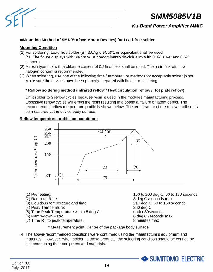
Reflow temperature profile and condition:
(1) Preheating: 150 to 200 deg.C, 60 to 120 seconds(2) Ramp-up Rate: 3 deg.C /seconds max(3) Liquidous temperature and time: 217 deg.C, 60 to 150 seconds(4) Peak Temperature: 260 deg.C(5) Time Peak Temperature within 5 deg.C: under 30seconds(6) Ramp-down Rate: 6 deg.C /seconds max(7) Time RT to peak temperature: 8 minutes max
* Measurement point: Center of the package body surface
(4) The above-recommended conditions were confirmed using the manufacture’s equipment and
materials. However, when soldering these products, the soldering condition should be verified by
customer using their equipment and materials.
200
217
(5)
(2)260255
RT
(1) (3)
150
Temperature(deg.C)
(6)
(7)

Edition 3.0
July. 201720
Ku-Band Power Amplifier MMIC
SMM5085V1B
CAUTION
This product contain gallium arsenide (GaAs) which can be hazardous to the human body and the environment. For
safety, observe the following procedures:
・Do not put these products into the mouth.
・Do not alter the form of this product into a gas, powder, or liquid through burning, crushing, or chemical processing as
these by-products are dangerous to the human body if inhaled, ingested, or swallowed.
・Observe government laws and company regulations when discarding this product. This product must be discarded in
accordance with methods specified by applicable hazardous waste procedures.


![BIP ŁÓDŹ · 2020. 4. 1. · Lp. Typ anteny Azymut Pasmo [MHz] 2100/900 2100/900 2100/900 1800/2600 1800/2600 1800/2600 2600 2600 2600 g\ównej tilt 3/4,75 3/ 3,25 3/ 4,75 4/4 4/4](https://img.pdfslide.tips/doc/110x75/60ef3052da019844c85be956/bip-d-2020-4-1-lp-typ-anteny-azymut-pasmo-mhz-2100900-2100900-2100900.jpg)