Embed Size (px)
Citation preview

KSZ8081MNX/RNB10BASE-T/100BASE-TX Physical Layer
Transceiver
Features• Single-chip 10Base-T/100Base-TX IEEE 802.3
compliant Ethernet transceiver• MII interface support (KSZ8081MNX)• RMII v1.2 Interface support with a 50 MHz refer-
ence clock output to MAC, and an option to input a 50 MHz reference clock (KSZ8081RNB)
• Back-to-back mode support for a 100 Mbps copper repeater
• MDC/MDIO management interface for PHY register configuration
• Programmable interrupt output• LED outputs for link, activity, and speed status
indication• On-chip termination resistors for the differential
pairs• Baseline wander correction• HP Auto MDI/MDI-X to reliably detect and correct
straight-through and crossover cable connections with disable and enable option
• Auto-negotiation to automatically select the highest link-up speed (10/100 Mbps) and duplex (half/full)
• Power-down and power-saving modes• LinkMD TDR-based cable diagnostics to identify
faulty copper cabling• Parametric NAND Tree support for fault detection
between chip I/Os and the board• HBM ESD rating (6 kV)• Loopback modes for diagnostics• Single 3.3V power supply with VDD I/O options
for 1.8V, 2.5V, or 3.3V• Built-in 1.2V regulator for core• Available in 32-pin (5 mm × 5 mm) QFN package
Applications• Game console• IP phone• IP set-top box• IP TV• LOM• Printer
2016 Microchip Technology Inc. DS00002202A-page 1

KSZ8081MNX/RNB
TO OUR VALUED CUSTOMERSIt is our intention to provide our valued customers with the best documentation possible to ensure successful use of your Microchipproducts. To this end, we will continue to improve our publications to better suit your needs. Our publications will be refined andenhanced as new volumes and updates are introduced. If you have any questions or comments regarding this publication, please contact the Marketing Communications Department viaE-mail at [email protected]. We welcome your feedback.
Most Current Data SheetTo obtain the most up-to-date version of this data sheet, please register at our Worldwide Web site at:
http://www.microchip.com
You can determine the version of a data sheet by examining its literature number found on the bottom outside corner of any page. The last character of the literature number is the version number, (e.g., DS30000000A is version A of document DS30000000).
ErrataAn errata sheet, describing minor operational differences from the data sheet and recommended workarounds, may exist for cur-rent devices. As device/documentation issues become known to us, we will publish an errata sheet. The errata will specify therevision of silicon and revision of document to which it applies.To determine if an errata sheet exists for a particular device, please check with one of the following:• Microchip’s Worldwide Web site; http://www.microchip.com• Your local Microchip sales office (see last page)When contacting a sales office, please specify which device, revision of silicon and data sheet (include -literature number) you areusing.
Customer Notification SystemRegister on our web site at www.microchip.com to receive the most current information on all of our products.
DS00002202A-page 2 2016 Microchip Technology Inc.

2016 Microchip Technology Inc. DS00002202A-page 3
KSZ8081MNX/RNBTable of Contents1.0 Introduction ..................................................................................................................................................................................... 42.0 Pin Description and Configuration ................................................................................................................................................... 53.0 Functional Description .................................................................................................................................................................. 154.0 Register Descriptions .................................................................................................................................................................... 345.0 Operational Characteristics ........................................................................................................................................................... 466.0 Electrical Characteristics ............................................................................................................................................................... 477.0 Timing Diagrams 498.0 Package Outline............................................................................................................................................................................. 60Appendix A: Data Sheet Revision History ........................................................................................................................................... 61The Microchip Web Site ...................................................................................................................................................................... 62Customer Change Notification Service ............................................................................................................................................... 62Customer Support ............................................................................................................................................................................... 62 Product Identification System ............................................................................................................................................................. 63

KSZ8081MNX/RNB
DS00002202A-page 4 2016 Microchip Technology Inc.
1.0 INTRODUCTION
1.1 General DescriptionThe KSZ8081 is a single-supply 10BASE-T/100BASE-TX Ethernet physical-layer transceiver for transmission andreception of data over standard CAT-5 unshielded twisted pair (UTP) cable.
The KSZ8081 is a highly-integrated PHY solution. It reduces board cost and simplifies board layout by using on-chiptermination resistors for the differential pairs and by integrating a low-noise regulator to supply the 1.2V core.
The KSZ8081MNX offers the Media Independent Interface (MII) and the KSZ8081RNB offers the Reduced Media Inde-pendent Interface (RMII) for direct connection with MII/RMII-compliant Ethernet MAC processors and switches.
A 25 MHz crystal is used to generate all required clocks, including the 50 MHz RMII reference clock output for theKSZ8081RNB.
The KSZ8081 provides diagnostic features to facilitate system bring-up and debugging in production testing and in prod-uct deployment. Parametric NAND tree support enables fault detection between KSZ8081 I/Os and the board. LinkMD®
TDR-based cable diagnostics identify faulty copper cabling.
The KSZ8081MNX and KSZ8081RNB are available in 32-pin, lead-free QFN packages.
FIGURE 1-1: FUNCTIONAL BLOCK DIAGRAM
KSZ8081MNX/KSZ8081RNB
MA
GN
ETI
CS
RJ-45CONNECTOR
MEDIA TYPES: 10BASE-T 100BASE-TX
ON
-CH
IP T
ER
MIN
ATI
ON
R
ES
ISTO
RS
MII/RMII
MDC/ MDIO MANAGEMENT
XO XI
25MHz XTAL
22pF 22pF
10/100MbpsMII/RMII MAC
50MHz(KSZ8081RNB)
REF_CLK

KSZ8081MNX/RNB
2.0 PIN DESCRIPTION AND CONFIGURATIONFIGURE 2-1: KSZ8081MNX 32-QFN PIN ASSIGNMENT (TOP VIEW)
TABLE 2-1: PIN DESCRIPTION — KSZ8081MNX
Pin Number Name
Buffer Type
(Note 2-1)Description
1 GND GND Ground
2 VDD_1.2 P 1.2V core VDD (power supplied by KSZ8081MNX). Decouple with 2.2 μF and 0.1 μF capacitors to ground.
3 VDDA_3.3 P 3.3V analog VDD.
4 RXM I/O Physical receive or transmit signal ( differential).
5 RXP I/O Physical receive or transmit signal (+ differential).
6 TXM I/O Physical transmit or receive signal ( differential).
7 TXP I/O Physical transmit or receive signal (+ differential).
GNDVDD_1.2
VDDA_3.3RXMRXPTXM
TXPXO
RX
D3/
PH
YAD
0M
DC
MD
IOR
EX
TXI
RX
D2/
PH
YAD
1R
XD
1/P
HYA
D2
RX
D0/
DU
PLE
X
1
2
3
4
5
6
7
8
9 10 11 12 13 14 15 16
24
23
22
21
20
19
18
17
32 31 30 29 28 27 26 25
TXD0TXENTXCINTRP/NAND_TREE#RXER/ISORXC/B-CAST_OFF
RXDV/CONFIG2VDDIO
CO
L/C
ON
FIG
0C
RS
/CO
NFI
G1
LED
0/N
WAY
EN
LED
1/S
PE
ED
RS
T#
TXD
3TX
D2
TXD
1
PADDLEGROUND
(ON BOTTOM OF CHIP)
2016 Microchip Technology Inc. DS00002202A-page 5

KSZ8081MNX/RNB
8 XO OCrystal feedback for 25 MHz crystal.This pin is a no connect if an oscillator or external clock source is used.
9 XI I Crystal / Oscillator / External Clock Input. 25 MHz ±50 ppm.
10 REXT I Set PHY transmit output current. Connect a 6.49 kΩ resistor to ground on this pin.
11 MDIO Ipu/Opu Management Interface (MII) Data I/O This pin has a weak pull-up, is open-drain, and requires an external 1.0 kΩ pull-up resistor.
12 MDC Ipu Management Interface (MII) Clock Input. This clock pin is synchro-nous to the MDIO data pin.
13 PHYAD0 Ipu/O
MII Mode: MII Receive Data Output[3].Config Mode: The pull-up/pull-down value is latched as PHY-ADDR[0] at the de-assertion of reset. See the Strap-In Options – KSZ8081MNX section for details.
14 PHYAD1 Ipd/O
MII Mode: MII Receive Data Output[2] (Note 2-2)Config Mode: The pull-up/pull-down value is latched as PHY-ADDR[1] at the de-assertion of reset. See the section Strap-In Options – KSZ8081MNX for details.
15 RXD1/PHYAD2 Ipd/O
MII Mode: MII Receive Data Output[1] (Note 2-2).Config Mode: The pull-up/pull-down value is latched as PHY-ADDR[2] at the de-assertion of reset. See the section Strap-In Options – KSZ8081MNX for details.
16 RXD0/DUPLEX Ipu/O
MII Mode: MII Receive Data Output[0] (Note 2-2).Config Mode: The pull-up/pull-down value is latched as DUPLEX at the de-assertion of reset.See the section Strap-In Options – KSZ8081MNX for details.
17 VDDIO P 3.3V, 2.5V, or 1.8V digital VDD.
18 RXDV/CONFIG2 Ipd/O
MII Mode: MII Receive Data Valid Output.Config Mode: The pull-up/pull-down value is latched as CONFIG2 at the de-assertion of reset.See the section Strap-In Options – KSZ8081MNX for details.
19 RXC/B-CAST_OFF Ipd/O
MII Mode: MII Receive Clock Output.Config Mode: The pull-up/pull-down value is latched as B-CAST_OFF at the de-assertion of reset. See the section Strap-In Options – KSZ8081MNX for details.
20 RXER/ISO Ipd/O
MII mode: MII Receive Error Output.Config Mode: The pull-up/pull-down value is latched as ISOLATE at the de-assertion of reset.See the section Strap-In Options – KSZ8081MNX for details.
TABLE 2-1: PIN DESCRIPTION — KSZ8081MNX (CONTINUED)
Pin Number Name
Buffer Type
(Note 2-1)Description
DS00002202A-page 6 2016 Microchip Technology Inc.

KSZ8081MNX/RNB
21
INTRP/
NAND_Tree#
Ipu/Opu
Interrupt Output: Programmable Interrupt Output.This pin has a weak pull-up, is open-drain, and requires an external 1.0 kΩ pull-up resistor.Config Mode: The pull-up/pull-down value is latched as NAND Tree# at the de-assertion of reset.See the section Strap-In Options – KSZ8081MNX for details.
22 TXC Ipd/O
MII Mode: MII Transmit Clock Output.At the de-assertion of reset, this pin needs to latch in a pull-down value for normal operation. If MAC side pulls this pin high, see Register 16h, Bit [15] for solution. It is better having an external pull-down resistor to avoid MAC side pulls this pin high.
23 TXEN I MII Mode: MII Transmit Enable input.
24 TXD0 I MII Mode: MII Transmit Data Input[0] (Note 2-4).
25 TXD1 I MII Mode: MII Transmit Data Input[1] (Note 2-4).
26 TXD2 I MII Mode: MII Transmit Data Input[2] (Note 2-4).
27 TXD3 I MII Mode: MII Transmit Data Input[3] (Note 2-4).
28 COL/CONFIG0
Ipd/O
MII Mode: MII Collision Detect output.Config Mode: The pull-up/pull-down value is latched as CONFIG0 at the de-assertion of reset. See the section Strap-In Options – KSZ8081MNX for details.
29 CRS/CONFIG1
Ipd/O
MII mode: MII Carrier Sense outputConfig mode: The pull-up/pull-down value is latched as CONFIG1 at the de-assertion of reset. See the section Strap-In Options – KSZ8081MNX for details.
30 LED0/NWAYEN Ipu/O
LED Output: Programmable LED0 Output.Config Mode: Latched as auto-negotiation enable (Register 0h, Bit [12]) at the de-assertion of reset. See the Strap-In Options – KSZ8081MNX section for details.The LED0 pin is programmable using Register 1Fh bits [5:4], and is defined as follows:
LED Mode = [10], [11] Reserved
TABLE 2-1: PIN DESCRIPTION — KSZ8081MNX (CONTINUED)
Pin Number Name
Buffer Type
(Note 2-1)Description
LED Mode = [00]
Link/Activity Pin State LED Definition
No link High OFF
Link Low ON
Activity Toggle Blinking
LED Mode = [01]
Link Pin State LED Definition
No link High OFF
Link Low ON
2016 Microchip Technology Inc. DS00002202A-page 7

KSZ8081MNX/RNB
Note 2-1 P = Power supply.GND = Ground.I = Input.O = Output.I/O = Bi-directional.Ipu = Input with internal pull-up (see Electrical Characteristics for value).Ipu/O = Input with internal pull-up (see Electrical Characteristics for value) during power-up/reset;output pin otherwise.Ipd/O = Input with internal pull-down (see Electrical Characteristics for value) during power-up/reset;output pin otherwise.Ipu/Opu = Input with internal pull-up (see Electrical Characteristics for value) and output with internalpull-up (see Electrical Characteristics for value).NC = Pin is not bonded to the die.
Note 2-2 RMII RX Mode: The RXD[1:0] bits are synchronous with the 50 MHz RMII Reference Clock. For eachclock period in which CRS_DV is asserted, two bits of recovered data are sent by the PHY to theMAC.
Note 2-3 RMII TX Mode: The TXD[1:0] bits are synchronous with the 50 MHz RMII Reference Clock. For eachclock period in which TXEN is asserted, two bits of data are received by the PHY from the MAC.
Note 2-4 MII TX Mode: The TXD[3:0] bits are synchronous with TXC. When TXEN is asserted, TXD[3:0]presents valid data from the MAC. TXD[3:0] has no effect on the PHY when TXEN is de-asserted.
31 LED1/SPEED Ipu/O
LED Output: Programmable LED1 Output.Config Mode: Latched as Speed (Register 0h, Bit [13]) at the de-assertion of reset. See the Strap-In Options – KSZ8081MNX section for details.The LED1 pin is programmable using Register 1Fh bits [5:4], and is defined as follows::
LED Mode = [10], [11]Reserved
32 RST# Ipu Chip Reset (active low).
PADDLE GND GND Ground.
TABLE 2-1: PIN DESCRIPTION — KSZ8081MNX (CONTINUED)
Pin Number Name
Buffer Type
(Note 2-1)Description
LED Mode = [00]
Speed Pin State LED Definition
10Base-T High OFF
100Base-TX Low ON
LED Mode = [01]
Activity Pin State LED Definition
No activity High OFF
Activity Toggle Blinking
DS00002202A-page 8 2016 Microchip Technology Inc.

KSZ8081MNX/RNB
STRAP-IN OPTIONS – KSZ8081MNXThe strap-in pins are latched at the de-assertion of reset. In some systems, the MAC RMII receive input pins may drivehigh/low during power-up or reset, and consequently cause the PHY strap-in pins on the RMII signals to be latched tounintended high/low states. In this case, external pull-ups (4.7 kΩ) or pull-downs (1.0 kΩ) should be added on thesePHY strap-in pins to ensure that the intended values are strapped-in correctly.Note 2-1 Ipu/O = Input with internal pull-up (see Electrical Characteristics for value) during power-up/reset;output pin otherwise.Ipd/O = Input with internal pull-down (see Electrical Characteristics for value) during power-up/reset;output pin otherwise.Ipu/Opu = Input with internal pull-up (see Electrical Characteristics for value) and output with internalpull-up (see Electrical Characteristics for value).
TABLE 2-2: STRAP-IN OPTIONS – KSZ8081MNX
Pin Number Pin Name
Type (Note 2-1)
Pin Function
151413
PHYAD2PHYAD1PHYAD0
Ipd/OIpd/OIpu/O
PHYAD[2:0] is latched at de-assertion of reset and is configurable to any value from 0 to 7 with PHY Address 1 as the default value.PHY Address 0 is assigned by default as the broadcast PHY address, but it can be assigned as a unique PHY address after pulling the B-CAST_OFF strap-in pin high or writing a ‘1’ to Register 16h, Bit [9].PHY Address bits [4:3] are set to 00 by default.
182928
CONFIG2CONFIG1CONFIG0
Ipd/OIpd/OIpd/O
The CONFIG[2:0] strap-in pins are latched at the de-assertion of reset.
20 ISO Ipd/O
Isolate modePull-up = EnablePull-down (default) = DisableAt the de-assertion of reset, this pin value is latched into Register 0h, Bit [10].
31 SPEED Ipu/O
Speed Mode:Pull-up (default) = 100 MbpsPull-down = 10 MbpsAt the de-assertion of reset, this pin value is latched into Register 0h, Bit [13] as the speed select, and also is latched into Register 4h (auto-negotiation adver-tisement) as the speed capability support.
16 DUPLEX Ipu/O
Duplex Mode:Pull-up (default) = Half-duplexPull-down = Full-duplexAt the de-assertion of reset, this pin value is latched into Register 0h, Bit [8].
30 NWAYEN Ipu/O
Nway auto-negotiation enablePull-up (default) = Enable auto-negotiationPull-down = Disable auto-negotiationAt the de-assertion of reset, this pin value is latched into Register 0h, Bit [12].
19 B-CAST_OFF Ipd/O
Broadcast off – for PHY Address 0Pull-up = PHY Address 0 is set as an unique PHY addressPull-down (default) = PHY Address 0 is set as a broadcast PHY addressAt the de-assertion of reset, this pin value is latched by the chip.
21 NAND_Tree# Ipu/Opu
NAND tree modePull-up (default) = DisablePull-down = EnableAt the de-assertion of reset, this pin value is latched by the chip.
CONFIG[2:0] Mode
001 RMII
101 RMII back-to-back
000, 010 – 100, 110, 111 Reserved – not used
2016 Microchip Technology Inc. DS00002202A-page 9

KSZ8081MNX/RNB
FIGURE 2-2: KSZ8081RNB 32-QFN PIN ASSIGNMENT (TOP VIEW)TABLE 2-3: PIN DESCRIPTION — KSZ8081RNBPin Number Pin Name Type (Note 2-1) Pin Function
1 GND GND Ground
2 VDD_1.2 P 1.2V core VDD (power supplied by KSZ8081RNB). Decouple with 2.2 μF and 0.1 μF capacitors to ground.
3 VDDA_3.3 P 3.3V analog VDD.4 RXM I/O Physical receive or transmit signal ( differential).5 RXP I/O Physical receive or transmit signal (+ differential).6 TXM I/O Physical transmit or receive signal ( differential).7 TXP I/O Physical transmit or receive signal (+ differential).
8 XO O Crystal feedback for 25 MHz crystal. This pin is a no con-nect if an oscillator or external clock source is used.
9 XI I
25 MHz Mode: 25 MHz ±50 ppm Crystal / Oscillator / External Clock Input 50 MHz Mode: 50 MHz ±50 ppm Oscillator / External Clock Input
10 REXT I Set PHY transmit output current. Connect a 6.49 kΩ resistor to ground on this pin.
11 MDIO Ipu/OpuManagement Interface (MII) Data I/O. This pin has a weak pull-up, is open-drain, and requires an external 1.0 kΩ pull-up resistor.
12 MDC Ipu Management Interface (MII) Clock Input. This clock pin is synchronous to the MDIO data pin.
13 PHYAD0 Ipu/O
The pull-up/pull-down value is latched as PHYADDR[0] at the de-assertion of reset. See the Strap-in Options – KSZ8081RNB section for details.
GNDVDD_1.2
VDDA_3.3RXMRXPTXM
TXPXO
PH
YAD
0M
DC
MD
IOR
EX
TXI
PH
YAD
1R
XD
1/P
HYA
D2
RX
D0/
DU
PLE
X
1
2
3
4
5
6
7
8
9 10 11 12 13 14 15 16
24
23
22
21
20
19
18
17
32 31 30 29 28 27 26 25
TXD0TXENNCINTRP/NAND_TREE#RXER/ISOREF_CLK/B-CAST_OFF
CRS_DV/CONFIG2VDDIO
CO
NFI
G0
CO
NFI
G1
LED
0/N
WAY
EN
LED
1/S
PE
ED
RS
T#
NC
NC
TXD
1
PADDLEGROUND
(ON BOTTOM OF CHIP)
DS00002202A-page 10 2016 Microchip Technology Inc.

KSZ8081MNX/RNB
14 PHYAD1 Ipd/O
The pull-up/pull-down value is latched as PHYADDR[1] at the de-assertion of reset. See the Strap-in Options – KSZ8081RNB section for details.
15 RXD1/PHYAD2 Ipd/O
RMII Mode: RMII Receive Data Output[1] (Note 2-2).Config Mode: The pull-up/pull-down value is latched as PHYADDR[2] at the de-assertion of reset. See the Strap-in Options – KSZ8081RNB section for details.
16 RXD0/DUPLEX Ipu/O
RMII Mode: RMII Receive Data Output[0] (Note 2-2).Config Mode: The pull-up/pull-down value is latched as DUPLEX at the de-assertion of reset. See the Strap-in Options – KSZ8081RNB section for details.
17 VDDIO P 3.3V, 2.5V, or 1.8V digital VDD.
18 CRS_DV/CONFIG2 Ipd/O
RMII Mode: RMII Carrier Sense/Receive Data Valid Out-put.Config Mode: The pull-up/pull-down value is latched as CONFIG2 at the de-assertion of reset. See the Strap-in Options – KSZ8081RNB section for details.
19
REF_CLK/
B-CAST_OFF
Ipd/O
RMII Mode: 25 MHz Mode: This pin provides the 50 MHz RMII refer-ence clock output to the MAC. See also XI (Pin 9).50 MHz mode: This pin is a no connect. See also XI (Pin 9).Config Mode: The pull-up/pull-down value is latched as B-CAST_OFF at the de-assertion of reset. See the Strap-in Options – KSZ8081RNB section for details.
20 RXER/ISO Ipd/O
RMII Mode: RMII Receive Error Output.Config Mode: The pull-up/pull-down value is latched as ISOLATE at the de-assertion of reset.See the Strap-in Options – KSZ8081RNB section for details.
21
INTRP/
NAND_Tree#
Ipu/Opu
Interrupt Output: Programmable Interrupt Output.This pin has a weak pull-up, is open-drain, and requires an external 1.0 kΩ pull-up resistor.Config Mode: The pull-up/pull-down value is latched as NAND Tree# at the de-assertion of reset. See the Strap-in Options – KSZ8081RNB section for details.
22 NC — No Connect. This pin is not bonded and can be left floating.
23 TXEN I RMII Transmit Enable input.24 TXD0 I RMII Transmit Data Input[0] (Note 2-3).25 TXD1 I RMII Transmit Data Input[1] (Note 2-3).
26 NC — No Connect. This pin is not bonded and can be left floating.
27 NC — No Connect. This pin is not bonded and can be left floating.
TABLE 2-3: PIN DESCRIPTION — KSZ8081RNBPin Number Pin Name Type (Note 2-1) Pin Function
2016 Microchip Technology Inc. DS00002202A-page 11

KSZ8081MNX/RNB
Note 2-1 P = Power supply. GND = Ground. I = Input. O = Output. I/O = Bi-directional. Ipu = Input with internalpull-up (see Electrical Characteristics for value). Ipu/O = Input with internal pull-up (see ElectricalCharacteristics for value) during power-up/reset; output pin otherwise. Ipd/O = Input with internal pull-down (see Electrical Characteristics for value) during power-up/reset; output pin otherwise. Ipu/Opu
28 CONFIG0 Ipd/OThe pull-up/pull-down value is latched as CONFIG0 at the de-assertion of reset. See the Strap-in Options – KSZ8081RNB section for details.
29 CONFIG1 Ipd/OThe pull-up/pull-down value is latched as CONFIG1 at the de-assertion of reset. See the Strap-in Options – KSZ8081RNB section for details.
30 LED0/NWAYEN Ipu/O
LED Output: Programmable LED0 Output.Config Mode: Latched as auto-negotiation enable (Regis-ter 0h, Bit [12]) at the de-assertion of reset. See the Strap-in Options – KSZ8081RNB section for details.The LED0 pin is programmable using Register 1Fh bits [5:4], and is defined as follows:
LED Mode = [10], [11] Reserved
31 LED1/ SPEED Ipu/O
LED Output: Programmable LED1 Output.Config Mode: Latched as Speed (Register 0h, Bit [13]) at the de-assertion of reset. See the Strap-in Options – KSZ8081RNB section for details.The LED1 pin is programmable using Register 1Fh bits [5:4], and is defined as follows:
LED Mode = [10], [11] Reserved32 RST# Ipu Chip Reset (active low).
PADDLE GND GND Ground.
TABLE 2-3: PIN DESCRIPTION — KSZ8081RNBPin Number Pin Name Type (Note 2-1) Pin Function
LED Mode = [00]
Link/Activity Pin State LED Definition
No link High OFF
Link Low ON
Activity Toggle Blinking
LED Mode = [01]
Link Pin State LED Definition
No link High OFF
Link Low ON
LED Mode = [00]
Speed Pin State LED Definition
10Base-T High OFF
100Base-TX Low ON
LED Mode = [01]
Activity Pin State LED Definition
No activity High OFF
Activity Toggle Blinking
DS00002202A-page 12 2016 Microchip Technology Inc.

KSZ8081MNX/RNB
= Input with internal pull-up (see Electrical Characteristics for value) and output with internal pull-up(see Electrical Characteristics for value). NC = Pin is not bonded to the die.Note 2-2 RMII RX Mode: The RXD[1:0] bits are synchronous with the 50 MHz RMII Reference Clock. For eachclock period in which CRS_DV is asserted, two bits of recovered data are sent by the PHY to theMAC.
Note 2-3 RMII TX Mode: The TXD[1:0] bits are synchronous with the 50MHz RMII Reference Clock. For eachclock period in which TXEN is asserted, two bits of data are received by the PHY from the MAC.
2016 Microchip Technology Inc. DS00002202A-page 13

KSZ8081MNX/RNB
STRAP-IN OPTIONS – KSZ8081RNBThe strap-in pins are latched at the de-assertion of reset. In some systems, the MAC RMII receive input pins may drivehigh/low during power-up or reset, and consequently cause the PHY strap-in pins on the RMII signals to be latched tounintended high/low states. In this case, external pull-ups (4.7 kΩ) or pull-downs (1.0 kΩ) should be added on thesePHY strap-in pins to ensure that the intended values are strapped-in correctly.Note 2-1 Ipu/O = Input with internal pull-up (see Electrical Characteristics for value) during power-up/reset;output pin otherwise.Ipd/O = Input with internal pull-down (see Electrical Characteristics for value) during power-up/reset;output pin otherwise.Ipu/Opu = Input with internal pull-up (see Electrical Characteristics for value) and output with internalpull-up (see Electrical Characteristics for value).
TABLE 2-4: STRAP-IN OPTIONS
Pin Number Pin Name
Type (Note 2-1)
Pin Function
151413
PHYAD2PHYAD1PHYAD0
Ipd/OIpd/OIpu/O
PHYAD[2:0] is latched at de-assertion of reset and is configurable to any value from 0 to 7 with PHY Address 1 as the default value.PHY Address 0 is assigned by default as the broadcast PHY address, but it can be assigned as a unique PHY address after pulling the B-CAST_OFF strapping pin high or writing a ‘1’ to Register 16h, Bit [9].PHY Address bits [4:3] are set to 00 by default.
182928
CONFIG2CONFIG1CONFIG0
Ipd/OIpd/OIpd/O
The CONFIG[2:0] strap-in pins are latched at the de-assertion of reset.
20 ISO Ipd/O
Isolate modePull-up = EnablePull-down (default) = DisableAt the de-assertion of reset, this pin value is latched into Register 0h, Bit [10].
31 SPEED Ipu/O
Speed modePull-up (default) = 100 MbpsPull-down = 10 MbpsAt the de-assertion of reset, this pin value is latched into Register 0h, Bit [13] as the speed select, and also is latched into Register 4h (auto-negotiation adver-tisement) as the speed capability support.
16 DUPLEX Ipu/O
Duplex modePull-up (default) = Half-duplexPull-down = Full-duplexAt the de-assertion of reset, this pin value is latched into Register 0h, Bit [8].
30 NWAYEN Ipu/O
Nway auto-negotiation enablePull-up (default) = Enable auto-negotiationPull-down = Disable auto-negotiationAt the de-assertion of reset, this pin value is latched into Register 0h, Bit [12].
19 B-CAST_OFF Ipd/O
Broadcast off – for PHY Address 0Pull-up = PHY Address 0 is set as an unique PHY addressPull-down (default) = PHY Address 0 is set as a broadcast PHY addressAt the de-assertion of reset, this pin value is latched by the chip.
21 NAND_Tree# Ipu/Opu
NAND tree modePull-up (default) = DisablePull-down = EnableAt the de-assertion of reset, this pin value is latched by the chip.
CONFIG[2:0] Mode
001 RMII
101 RMII back-to-back
000, 010 – 100, 110, 111 Reserved – not used
DS00002202A-page 14 2016 Microchip Technology Inc.

KSZ8081MNX/RNB
3.0 FUNCTIONAL DESCRIPTION3.1 10BASE-T/100BASE-TX TransceiverThe KSZ8081 is an integrated single 3.3V supply Fast Ethernet transceiver. It is fully compliant with the IEEE 802.3Specification, and reduces board cost and simplifies board layout by using on-chip termination resistors for the two dif-ferential pairs and by integrating the regulator to supply the 1.2V core.
On the copper media side, the KSZ8081 supports 10BASE-T and 100BASE-TX for transmission and reception of dataover a standard CAT-5 unshielded twisted pair (UTP) cable, and HP Auto MDI/MDI–X for reliable detection of and cor-rection for straight-through and crossover cables.
On the MAC processor side, the KSZ8081MNX offers the Media Independent Interface (MII) and the KSZ8081RNBoffers the Reduced Media Independent Interface (RMII) for direct connection with MII and RMII compliant Ethernet MACprocessors and switches, respectively.
The MII management bus option gives the MAC processor complete access to the KSZ8081 control and status regis-ters. Additionally, an interrupt pin eliminates the need for the processor to poll for PHY status change.
The KSZ8081MNX/RNB is used to refer to both KSZ8081MNX and KSZ8081RNB versions in this datasheet.
3.1.1 100BASE-TX TRANSMITThe 100BASE-TX transmit function performs parallel-to-serial conversion, 4B/5B encoding, scrambling, NRZ-to-NRZIconversion, and MLT3 encoding and transmission.
The circuitry starts with a parallel-to-serial conversion, which converts the MII data from the MAC into a 125 MHz serialbit stream. The data and control stream is then converted into 4B/5B coding and followed by a scrambler. The serializeddata is further converted from NRZ-to-NRZI format, and then transmitted in MLT3 current output. The output current isset by an external 6.49 kΩ 1% resistor for the 1:1 transformer ratio.
The output signal has a typical rise/fall time of 4 ns and complies with the ANSI TP-PMD standard regarding amplitudebalance, overshoot, and timing jitter. The wave-shaped 10BASE-T output is also incorporated into the 100BASE-TXtransmitter.
3.1.2 100BASE-TX RECEIVEThe 100BASE-TX receiver function performs adaptive equalization, DC restoration, MLT3-to-NRZI conversion, data andclock recovery, NRZI-to-NRZ conversion, de-scrambling, 4B/5B decoding, and serial-to-parallel conversion.
The receiving side starts with the equalization filter to compensate for inter-symbol interference (ISI) over the twistedpair cable. Because the amplitude loss and phase distortion is a function of the cable length, the equalizer must adjustits characteristics to optimize performance. In this design, the variable equalizer makes an initial estimation based oncomparisons of incoming signal strength against some known cable characteristics, then tunes itself for optimization.This is an ongoing process and self-adjusts against environmental changes such as temperature variations.
Next, the equalized signal goes through a DC-restoration and data-conversion block. The DC-restoration circuit com-pensates for the effect of baseline wander and improves the dynamic range. The differential data-conversion circuit con-verts MLT3 format back to NRZI. The slicing threshold is also adaptive.
The clock-recovery circuit extracts the 125 MHz clock from the edges of the NRZI signal. This recovered clock is thenused to convert the NRZI signal to NRZ format. This signal is sent through the de-scrambler, then the 4B/5B decoder.Finally, the NRZ serial data is converted to MII format and provided as the input data to the MAC.
3.1.3 SCRAMBLER/DE-SCRAMBLER (100BASE-TX ONLY)The scrambler spreads the power spectrum of the transmitted signal to reduce electromagnetic interference (EMI) andbaseline wander. The de-scrambler recovers the scrambled signal.
3.1.4 10BASE-T TRANSMITThe 10BASE-T drivers are incorporated with the 100BASE-TX drivers to allow for transmission using the same mag-netic. The drivers perform internal wave shaping and pre-emphasis, and output 10BASE-T signals with a typical ampli-tude of 2.5V peak. The 10BASE-T signals have harmonic contents that are at least 27 dB below the fundamentalfrequency when driven by an all-ones Manchester-encoded signal.
2016 Microchip Technology Inc. DS00002202A-page 15

KSZ8081MNX/RNB
3.1.5 10BASE-T RECEIVEOn the receive side, input buffer and level detecting squelch circuits are used. A differential input receiver circuit and aphase-locked loop (PLL) performs the decoding function. The Manchester-encoded data stream is separated into clocksignal and NRZ data. A squelch circuit rejects signals with levels less than 400 mV, or with short pulse widths, to preventnoise at the RXP and RXM inputs from falsely triggering the decoder. When the input exceeds the squelch limit, the PLLlocks onto the incoming signal and the KSZ8081MNX/RNB decodes a data frame. The receive clock is kept activeduring idle periods between data receptions.3.1.6 SQE AND JABBER FUNCTION (10BASE-T ONLY)In 10BASE-T operation, a short pulse is put out on the COL pin after each frame is transmitted. This SQE test is neededto test the 10BASE-T transmit/receive path. If transmit enable (TXEN) is high for more than 20 ms (jabbering), the10BASE-T transmitter is disabled and COL is asserted high. If TXEN is then driven low for more than 250 ms, the10BASE-T transmitter is re-enabled and COL is de-asserted (returns to low).
3.1.7 PLL CLOCK SYNTHESIZERThe KSZ8081MNX/RNB generates all internal clocks and all external clocks for system timing from an external 25 MHzcrystal, oscillator, or reference clock. For the KSZ8081RNB in RMII 50 MHz clock mode, these clocks are generatedfrom an external 50 MHz oscillator or system clock.
3.1.8 AUTO-NEGOTIATIONThe KSZ8081MNX/RNB conforms to the auto-negotiation protocol, defined in Clause 28 of the IEEE 802.3 Specification.
Auto-negotiation allows unshielded twisted pair (UTP) link partners to select the highest common mode of operation.
During auto-negotiation, link partners advertise capabilities across the UTP link to each other and then compare theirown capabilities with those they received from their link partners. The highest speed and duplex setting that is commonto the two link partners is selected as the mode of operation.
The following list shows the speed and duplex operation mode from highest to lowest priority.
• Priority 1: 100BASE-TX, full–duplex• Priority 2: 100BASE-TX, half–duplex• Priority 3: 10BASE-T, full–duplex• Priority 4: 10BASE-T, half–duplex
If auto-negotiation is not supported or the KSZ8081MNX/RNB link partner is forced to bypass auto-negotiation, then theKSZ8081MNX/RNB sets its operating mode by observing the signal at its receiver. This is known as parallel detection,which allows the KSZ8081MNX/RNB to establish a link by listening for a fixed signal protocol in the absence of the auto-negotiation advertisement protocol.
Auto-negotiation is enabled by either hardware pin strapping (NWAYEN, Pin 42) or software (Register 0h, Bit [12]).
By default, auto-negotiation is enabled after power-up or hardware reset. After that, auto-negotiation can be enabled ordisabled by Register 0h, Bit [12]. If auto-negotiation is disabled, the speed is set by Register 0h, Bit [13], and the duplexis set by Register 0h, Bit [8].
The auto-negotiation link-up process is shown in Figure 3-1.
DS00002202A-page 16 2016 Microchip Technology Inc.

KSZ8081MNX/RNB
FIGURE 3-1: AUTO-NEGOTIATION FLOW CHART3.2 MII Interface (KSZ8081MNX Only)The Media Independent Interface (MII) is compliant with the IEEE 802.3 Specification. It provides a common interfacebetween MII PHYs and MACs, and has the following key characteristics:
• Pin count is 15 pins (6 pins for data transmission, 7 pins for data reception, and 2 pins for carrier and collision indication).
• 10 Mbps and 100 Mbps data rates are supported at both half- and full-duplex.• Data transmission and reception are independent and belong to separate signal groups.• Transmit data and receive data are each 4 bits wide, a nibble.
By default, the KSZ8081MNX is configured to MII mode after it is powered up or hardware reset with the following:
A 25 MHz crystal connected to XI, XO (pins 9, 8), or an external 25 MHz clock source (oscillator) connected to XI.
The CONFIG[2:0] strapping pins (pins 18, 29, 28) set to 000 (default setting).
START AUTO-NEGOTIATION
FORCE LINK SETTING
LISTEN FOR 10BASE-T LINK PULSES
LISTEN FOR 100BASE-TXIDLES
ATTEMPT AUTO-NEGOTIATION
LINK MODE SET
BYPASS AUTO-NEGOTIATIONAND SET LINK MODE
LINK MODE SET?
PARALLELOPERATIONNO
YES
YES
NO
JOIN FLOW
2016 Microchip Technology Inc. DS00002202A-page 17

KSZ8081MNX/RNB
3.2.1 MII SIGNAL DEFINITIONTable 3-1 describes the MII signals. Refer to Clause 22 of the IEEE 802.3 Specification for detailed information.3.2.2 TRANSMIT CLOCK (TXC)TXC is sourced by the PHY. It is a continuous clock that provides the timing reference for TXEN and TXD[3:0]. TXC is2.5 MHz for 10 Mbps operation and 25 MHz for 100 Mbps operation.
3.2.3 TRANSMIT ENABLE (TXEN)TXEN indicates that the MAC is presenting nibbles on TXD[3:0] for transmission. It is asserted synchronously with thefirst nibble of the preamble and remains asserted while all nibbles to be transmitted are presented on the MII. It isnegated before the first TXC following the final nibble of a frame.
TXEN transitions synchronously with respect to TXC.
3.2.4 TRANSMIT DATA[3:0] (TXD[3:0])TXD[3:0] transitions synchronously with respect to TXC. When TXEN is asserted, TXD[3:0] are accepted by the PHYfor transmission. TXD[3:0] is 00 to indicate idle when TXEN is de-asserted. Values other than 00 on TXD[3:0] whileTXEN is de-asserted are ignored by the PHY.
3.2.5 RECEIVE CLOCK (RXC)RXC provides the timing reference for RXDV, RXD[3:0], and RXER.
• In 10 Mbps mode, RXC is recovered from the line while the carrier is active. RXC is derived from the PHY’s refer-ence clock when the line is idle or the link is down.
• In 100 Mbps mode, RXC is continuously recovered from the line. If the link is down, RXC is derived from the PHY’s reference clock.
RXC is 2.5 MHz for 10 Mbps operation and 25 MHz for 100 Mbps operation.
3.2.6 RECEIVE DATA VALID (RXDV)RXDV is driven by the PHY to indicate that the PHY is presenting recovered and decoded nibbles on RXD[3:0].
• In 10 Mbps mode, RXDV is asserted with the first nibble of the start-of-frame delimiter (SFD), 5D, and remains asserted until the end of the frame.
• In 100 Mbps mode, RXDV is asserted from the first nibble of the preamble to the last nibble of the frame.
RXDV transitions synchronously with respect to RXC.
TABLE 3-1: MII SIGNAL DEFINITION
MII Signal Name
Direction (with respect to PHY,
KSZ8081MNX signal)
Direction (with respect to MAC) Description
TXC Output Input Transmit Clock(2.5 MHz for 10 Mbps; 25 MHz for 100 Mbps)
TXEN Input Output Transmit EnableTXD[3:0] Input Output Transmit Data[3:0]
RXC Output Input Receive Clock (2.5 MHz for 10 Mbps; 25 MHz for 100 Mbps)
RXDV Output Input Receive Data ValidRXD[3:0] Output Input Receive Data[3:0]RXER Output Input, or (not required) Receive ErrorCRS Output Input Carrier SenseCOL Output Input Collision Detection
DS00002202A-page 18 2016 Microchip Technology Inc.

KSZ8081MNX/RNB
3.2.7 RECEIVE DATA[3:0] (RXD[3:0])RXD[3:0] transitions synchronously with respect to RXC. For each clock period in which RXDV is asserted, RXD[3:0]transfers a nibble of recovered data from the PHY.3.2.8 RECEIVE ERROR (RXER)RXER is asserted for one or more RXC periods to indicate that a symbol error (for example, a coding error that a PHYcan detect that may otherwise be undetectable by the MAC sub-layer) was detected somewhere in the frame beingtransferred from the PHY.
RXER transitions synchronously with respect to RXC. While RXDV is de-asserted, RXER has no effect on the MAC.
3.2.9 CARRIER SENSE (CRS)CRS is asserted and de-asserted as follows:
• In 10 Mbps mode, CRS assertion is based on the reception of valid preambles. CRS de-assertion is based on the reception of an end-of-frame (EOF) marker.
• In 100 Mbps mode, CRS is asserted when a start-of-stream delimiter or /J/K symbol pair is detected. CRS is de-asserted when an end-of-stream delimiter or /T/R symbol pair is detected. Additionally, the PMA layer de-asserts CRS if IDLE symbols are received without /T/R.
3.2.10 COLLISION (COL)COL is asserted in half-duplex mode whenever the transmitter and receiver are simultaneously active on the line. Thisinforms the MAC that a collision has occurred during its transmission to the PHY. COL transitions asynchronously withrespect to TXC and RXC.
3.2.11 MII SIGNAL DIAGRAMThe KSZ8081MNX MII pin connections to the MAC are shown in Figure 3-2.
FIGURE 3-2: KSZ8081MNX MII INTERFACE
TXC
TX_EN
TXD[3:0]
TXC
TX_EN
TXD[3:0]
RXD[3:0] RXD[3:0]
RXC
RXDV
RXC
RXDV
CRS
COL
CRS
COL
RXER RXER
2016 Microchip Technology Inc. DS00002202A-page 19
KSZ8081MNX/RNB
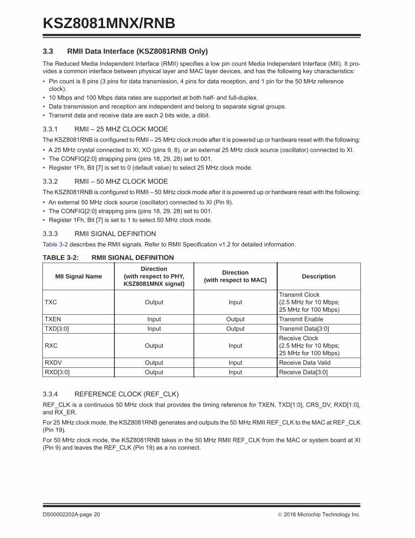
3.3 RMII Data Interface (KSZ8081RNB Only)The Reduced Media Independent Interface (RMII) specifies a low pin count Media Independent Interface (MII). It pro-vides a common interface between physical layer and MAC layer devices, and has the following key characteristics:• Pin count is 8 pins (3 pins for data transmission, 4 pins for data reception, and 1 pin for the 50 MHz reference clock).
• 10 Mbps and 100 Mbps data rates are supported at both half- and full-duplex.• Data transmission and reception are independent and belong to separate signal groups.• Transmit data and receive data are each 2 bits wide, a dibit.
3.3.1 RMII – 25 MHZ CLOCK MODEThe KSZ8081RNB is configured to RMII – 25 MHz clock mode after it is powered up or hardware reset with the following:
• A 25 MHz crystal connected to XI, XO (pins 9, 8), or an external 25 MHz clock source (oscillator) connected to XI.• The CONFIG[2:0] strapping pins (pins 18, 29, 28) set to 001.• Register 1Fh, Bit [7] is set to 0 (default value) to select 25 MHz clock mode.
3.3.2 RMII – 50 MHZ CLOCK MODEThe KSZ8081RNB is configured to RMII – 50 MHz clock mode after it is powered up or hardware reset with the following:
• An external 50 MHz clock source (oscillator) connected to XI (Pin 9).• The CONFIG[2:0] strapping pins (pins 18, 29, 28) set to 001.• Register 1Fh, Bit [7] is set to 1 to select 50 MHz clock mode.
3.3.3 RMII SIGNAL DEFINITIONTable 3-2 describes the RMII signals. Refer to RMII Specification v1.2 for detailed information.
3.3.4 REFERENCE CLOCK (REF_CLK)REF_CLK is a continuous 50 MHz clock that provides the timing reference for TXEN, TXD[1:0], CRS_DV, RXD[1:0],and RX_ER.
For 25 MHz clock mode, the KSZ8081RNB generates and outputs the 50 MHz RMII REF_CLK to the MAC at REF_CLK(Pin 19).
For 50 MHz clock mode, the KSZ8081RNB takes in the 50 MHz RMII REF_CLK from the MAC or system board at XI(Pin 9) and leaves the REF_CLK (Pin 19) as a no connect.
TABLE 3-2: RMII SIGNAL DEFINITION
MII Signal NameDirection
(with respect to PHY, KSZ8081MNX signal)
Direction (with respect to MAC) Description
TXC Output InputTransmit Clock (2.5 MHz for 10 Mbps; 25 MHz for 100 Mbps)
TXEN Input Output Transmit EnableTXD[3:0] Input Output Transmit Data[3:0]
RXC Output InputReceive Clock (2.5 MHz for 10 Mbps; 25 MHz for 100 Mbps)
RXDV Output Input Receive Data ValidRXD[3:0] Output Input Receive Data[3:0]
DS00002202A-page 20 2016 Microchip Technology Inc.

KSZ8081MNX/RNB
3.3.5 TRANSMIT ENABLE (TXEN)TXEN indicates that the MAC is presenting dibits on TXD[1:0] for transmission. It is asserted synchronously with the firstdibit of the preamble and remains asserted while all dibits to be transmitted are presented on the RMII. It is negatedbefore the first REF_CLK following the final dibit of a frame.TXEN transitions synchronously with respect to REF_CLK.
3.3.6 TRANSMIT DATA[1:0] (TXD[1:0])TXD[1:0] transitions synchronously with respect to REF_CLK. When TXEN is asserted, the PHY accepts TXD[1:0] fortransmission.
TXD[1:0] is 00 to indicate idle when TXEN is de-asserted. The PHY ignores values other than 00 on TXD[1:0] whileTXEN is de-asserted.
3.3.7 CARRIER SENSE/RECEIVE DATA VALID (CRS_DV)The PHY asserts CRS_DV when the receive medium is non-idle. It is asserted asynchronously when a carrier isdetected. This happens when squelch is passed in 10 Mbps mode, and when two non-contiguous 0s in 10 bits aredetected in 100 Mbps mode. Loss of carrier results in the de-assertion of CRS_DV.
While carrier detection criteria are met, CRS_DV remains asserted continuously from the first recovered dibit of theframe through the final recovered dibit. It is negated before the first REF_CLK that follows the final dibit. The data onRXD[1:0] is considered valid after CRS_DV is asserted. However, because the assertion of CRS_DV is asynchronousrelative to REF_CLK, the data on RXD[1:0] is 00 until receive signals are properly decoded.
3.3.8 RECEIVE DATA[1:0] (RXD[1:0])RXD[1:0] transitions synchronously with respect to REF_CLK. For each clock period in which CRS_DV is asserted,RXD[1:0] transfers two bits of recovered data from the PHY.
RXD[1:0] is 00 to indicate idle when CRS_DV is de-asserted. The MAC ignores values other than 00 on RXD[1:0] whileCRS_DV is de-asserted.
3.3.9 RECEIVE ERROR (RXER)RXER is asserted for one or more REF_CLK periods to indicate that a symbol error (for example, a coding error that aPHY can detect that may otherwise be undetectable by the MAC sub-layer) was detected somewhere in the frame beingtransferred from the PHY.
RXER transitions synchronously with respect to REF_CLK. . While CRS_DV is de-asserted, RXER has no effect on theMAC.
3.3.10 COLLISION DETECTION (COL)The MAC regenerates the COL signal of the MII from TXEN and CRS_DV.
3.3.11 RMII SIGNAL DIAGRAMThe KSZ8081RNB RMII pin connections to the MAC for 25 MHz clock mode are shown in Figure 3-3. The connectionsfor 50 MHz clock mode are shown in Figure 3-4.
2016 Microchip Technology Inc. DS00002202A-page 21

KSZ8081MNX/RNB
FIGURE 3-3: KSZ8081RNB RMII INTERFACE (25 MHZ CLOCK MODE)FIGURE 3-4: KSZ8081RNB RMII INTERFACE (50 MHZ CLOCK MODE)
KSZ8081RNB
CRS_DV
RXD[1:0]
RXER
TXD[1:0]
RMII MAC
CRS_DV
RXD[1:0]
TXD[1:0]
RX_ER
REF_CLK REF_CLK
TXEN TX_EN
XO XI
25MHzXTAL
22pF 22pF
KSZ8081RNB
CRS_DV
RXD[1:0]
RXER
TXD[1:0]
RMII MAC
CRS_DV
RXD[1:0]
TXD[1:0]
RX_ER
REF_CLK
TXEN TX_EN
XI
50MHzOSC
DS00002202A-page 22 2016 Microchip Technology Inc.
KSZ8081MNX/RNB
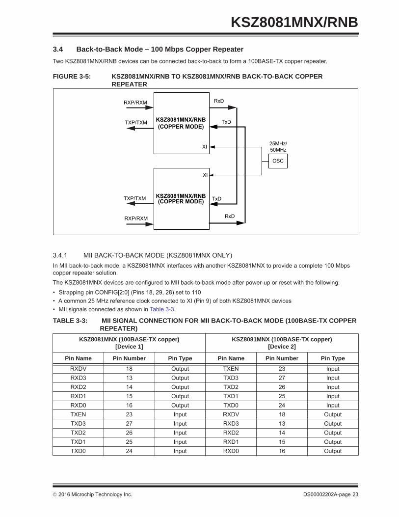
3.4 Back-to-Back Mode – 100 Mbps Copper RepeaterTwo KSZ8081MNX/RNB devices can be connected back-to-back to form a 100BASE-TX copper repeater.FIGURE 3-5: KSZ8081MNX/RNB TO KSZ8081MNX/RNB BACK-TO-BACK COPPER REPEATER
3.4.1 MII BACK-TO-BACK MODE (KSZ8081MNX ONLY)In MII back-to-back mode, a KSZ8081MNX interfaces with another KSZ8081MNX to provide a complete 100 Mbps copper repeater solution.
The KSZ8081MNX devices are configured to MII back-to-back mode after power-up or reset with the following:
• Strapping pin CONFIG[2:0] (Pins 18, 29, 28) set to 110• A common 25 MHz reference clock connected to XI (Pin 9) of both KSZ8081MNX devices• MII signals connected as shown in Table 3-3.
TABLE 3-3: MII SIGNAL CONNECTION FOR MII BACK-TO-BACK MODE (100BASE-TX COPPER REPEATER)
KSZ8081MNX (100BASE-TX copper)[Device 1]
KSZ8081MNX (100BASE-TX copper)[Device 2]
Pin Name Pin Number Pin Type Pin Name Pin Number Pin Type
RXDV 18 Output TXEN 23 InputRXD3 13 Output TXD3 27 InputRXD2 14 Output TXD2 26 InputRXD1 15 Output TXD1 25 InputRXD0 16 Output TXD0 24 InputTXEN 23 Input RXDV 18 OutputTXD3 27 Input RXD3 13 OutputTXD2 26 Input RXD2 14 OutputTXD1 25 Input RXD1 15 OutputTXD0 24 Input RXD0 16 Output
KSZ8081MNX/RNB(COPPER MODE)
RXP/RXM
TXP/TXM
RxD
TxD
RxD
TxD
OSC
XI
XI
25MHz/50MHz
TXP/TXM
RXP/RXM
(COPPER MODE)KSZ8081MNX/RNB
2016 Microchip Technology Inc. DS00002202A-page 23

KSZ8081MNX/RNB
3.5 MII Management (MIIM) InterfaceThe KSZ8081MNX/RNB supports the IEEE 802.3 MII management interface, also known as the Management DataInput/Output (MDIO) interface. This interface allows an upper-layer device, such as a MAC processor, to monitor andcontrol the state of the KSZ8081MNX/RNB. An external device with MIIM capability is used to read the PHY status and/or configure the PHY settings. More details about the MIIM interface can be found in Clause 22.2.4 of the IEEE 802.3Specification.The MIIM interface consists of the following:
• A physical connection that incorporates the clock line (MDC) and the data line (MDIO).• A specific protocol that operates across the physical connection mentioned earlier, which allows the external
controller to communicate with one or more PHY devices.• A set of 16-bit MDIO registers. Registers [0:8] are standard registers, and their functions are defined in the IEEE
802.3 Specification. The additional registers are provided for expanded functionality. See the “Register Map” section for details.
As the default, the KSZ8081MNX/RNB supports unique PHY addresses 1 to 7, and broadcast PHY address 0. The latteris defined in the IEEE 802.3 Specification, and can be used to read/write to a single KSZ8081MNX/RNB device, or writeto multiple KSZ8081MNX/RNB devices simultaneously.
PHY address 0 can optionally be disabled as the broadcast address by either hardware pin strapping (B-CAST_OFF,Pin 19) or software (Register 16h, Bit [9]), and assigned as a unique PHY address.
The PHYAD[2:0] strapping pins are used to assign a unique PHY address between 0 and 7 to each KSZ8081MNX/RNBdevice.
The MIIM interface can operates up to a maximum clock speed of 10 MHz MAC clock.
Table 3-4 shows the MII management frame format for the KSZ8081MNX/RNB.
3.6 Interrupt (INTRP)INTRP (Pin 21) is an optional interrupt signal that is used to inform the external controller that there has been a statusupdate to the KSZ8081MNX/RNB PHY register. Bits [15:8] of Register 1Bh are the interrupt control bits to enable anddisable the conditions for asserting the INTRP signal. Bits [7:0] of Register 1Bh are the interrupt status bits to indicatewhich interrupt conditions have occurred. The interrupt status bits are cleared after reading Register 1Bh.
Bit [9] of Register 1Fh sets the interrupt level to active high or active low. The default is active low.
The MII management bus option gives the MAC processor complete access to the KSZ8081MNX/RNB control and sta-tus registers. Additionally, an interrupt pin eliminates the need for the processor to poll the PHY for status change.
3.7 HP Auto MDI/MDI-XHP Auto MDI/MDI-X configuration eliminates the need to decide whether to use a straight cable or a crossover cablebetween the KSZ8081MNX/RNB and its link partner. This feature allows the KSZ8081MNX/RNB to use either type ofcable to connect with a link partner that is in either MDI or MDI-X mode. The auto-sense function detects transmit andreceive pairs from the link partner and assigns transmit and receive pairs to the KSZ8081MNX/RNB accordingly.
HP Auto MDI/MDI-X is enabled by default. It is disabled by writing a ‘1’ to Register 1Fh, Bit [13]. MDI and MDI-X modeis selected by Register 1Fh, Bit [14] if HP Auto MDI/MDI-X is disabled.
An isolation transformer with symmetrical transmit and receive data paths is recommended to support Auto MDI/MDI-X.
Table 3-5 shows how the IEEE 802.3 Standard defines MDI and MDI-X.
TABLE 3-4: MII MANAGEMENT FRAME FORMAT FOR THE KSZ8081MNX/RNB
Preamble Start of Frame
Read/Write OP
Code
PHY AddressBits [4:0]
REG AddressBits [4:0]
TA DataBits [15:0] Idle
Read 32 1’s 01 10 00AAA RRRRR Z0 DDDDDDDD_DDDDDDDD ZWrite 32 1’s 01 01 00AAA RRRRR 10 DDDDDDDD_DDDDDDDD Z
DS00002202A-page 24 2016 Microchip Technology Inc.

KSZ8081MNX/RNB
3.7.1 STRAIGHT CABLEA straight cable connects an MDI device to an MDI-X device, or an MDI-X device to an MDI device. Figure 3-6 showsa typical straight cable connection between a NIC card (MDI device) and a switch or hub (MDI-X device).
FIGURE 3-6: TYPICAL STRAIGHT CABLE CONNECTION
3.7.2 CROSSOVER CABLEA crossover cable connects an MDI device to another MDI device, or an MDI-X device to another MDI-X device.Figure 3-7 shows a typical crossover cable connection between two switches or hubs (two MDI-X devices).
FIGURE 3-7: TYPICAL CROSSOVER CABLE CONNECTION
TABLE 3-5: MDI/MDI-X PIN DEFINITIONMDI MDI-X
RJ-45 Pin Signal RJ-45 Pin Signal
1 TX+ 1 RX+2 TX– 2 RX–3 RX+ 3 TX+6 RX– 6 TX–
RECEIVE PAIR TRANSMIT PAIR
RECEIVE PAIR
1
2
3
4
5
6
7
8
1 2 3 4 5 6 7 8
TRANSMIT PAIR
MODULAR CONNECTOR (RJ-45)
NIC
STRAIGHT CABLE
10/100 ETHERNET MEDIA DEPENDENT INTERFACE
10/100 ETHERNET MEDIA DEPENDENT INTERFACE
MODULAR CONNECTOR (RJ-45)
HUB(REPEATER OR SWITCH)
RECEIVE PAIR RECEIVE PAIR
TRANSMIT PAIR
1
2
3
4
5
6
7
8
1
2
3
4
5
6
7
8
TRANSMIT PAIR
10/100 ETHERNETMEDIA DEPENDENT INTERFACE
10/100 ETHERNETMEDIA DEPENDENT INTERFACE
MODULAR CONNECTOR (RJ-45)
HUB(REPEATER OR SWITCH)
CROSSOVERCABLE
MODULAR CONNECTOR (RJ-45)
HUB(REPEATER OR SWITCH)
2016 Microchip Technology Inc. DS00002202A-page 25

KSZ8081MNX/RNB
3.8 Loopback ModeThe KSZ8081MNX/RNB supports the following loopback operations to verify analog and/or digital data paths.• Local (digital) loopback• Remote (analog) loopback
3.8.1 LOCAL (DIGITAL) LOOPBACKThis loopback mode checks the MII/RMII transmit and receive data paths between the KSZ8081MNX/RNB and theexternal MAC, and is supported for both speeds (10 Mbps/100 Mbps) at full-duplex.
The loopback data path is shown in Figure 3-8.
1. The MII/RMII MAC transmits frames to the KSZ8081MNX/RNB.2. Frames are wrapped around inside the KSZ8081MNX/RNB.3. The KSZ8081MNX/RNB transmits frames back to the MII/RMII MAC.4. Except the frames back to the RMII MAC, the transmit frames also go out from the copper port.
FIGURE 3-8: LOCAL (DIGITAL) LOOPBACK
The following programming action and register settings are used for local loopback mode.
For 10 Mbps/100 Mbps loopback,
•Set Register 0h,
Bit [14] = 1 // Enable local loopback mode
Bit [13] = 0/1 // Select 10 Mbps/100 Mbps speed
Bit [12] = 0 // Disable auto-negotiation
Bit [8] = 1 // Select full-duplex mode
The following steps should be applied if unwanted frames appear outside the copper port in the local feedback.
1. Set register 1Fh bit [3] to ‘1’ to disable the transmitter.2. Run local loopback test as above.3. Set register 1Fh bit [3] to ‘0’ to enable the transmitter.
MII/RMIIMAC
MII/RMII
AFE
(ANALOG)
KSZ8081MNX/RNB
PCS
(DIGITAL)
DS00002202A-page 26 2016 Microchip Technology Inc.

KSZ8081MNX/RNB
3.8.2 REMOTE (ANALOG) LOOPBACKThis loopback mode checks the line (differential pairs, transformer, RJ-45 connector, Ethernet cable) transmit andreceive data paths between the KSZ8081MNX/RNB and its link partner, and is supported for 100BASE-TX full-duplexmode only.The loopback data path is shown in Figure 3-9.
1. The Fast Ethernet (100BASE-TX) PHY link partner transmits frames to the KSZ8081MNX/RNB.2. Frames are wrapped around inside the KSZ8081MNX/RNB.3. The KSZ8081MNX/RNB transmits frames back to the Fast Ethernet (100BASE-TX) PHY link partner.
FIGURE 3-9: REMOTE (ANALOG) LOOPBACK
The following programming steps and register settings are used for remote loopback mode.
1.Set Register 0h,
Bits [13] = 1 // Select 100 Mbps speed
Bit [12] = 0 // Disable auto-negotiation
Bit [8] = 1 // Select full-duplex mode
or just auto-negotiate and link up at 100BASE-TX full-duplex mode with the link partner.
2.Set Register 1Fh,
Bit [2] = 1 // Enable remote loopback mode
RJ-45
RJ-45
CAT-5(UTP)
KSZ8081MNX/RNB
100BASE-TXLINK PARTNER
AFE(ANALOG)
PCS(DIGITAL)
MII/RMII
2016 Microchip Technology Inc. DS00002202A-page 27

KSZ8081MNX/RNB
3.9 LinkMD® Cable DiagnosticThe LinkMD function uses time-domain reflectometry (TDR) to analyze the cabling plant for common cabling problems.These include open circuits, short circuits, and impedance mismatches.LinkMD works by sending a pulse of known amplitude and duration down the MDI or MDI-X pair, then analyzing theshape of the reflected signal to determine the type of fault. The time duration for the reflected signal to return providesthe approximate distance to the cabling fault. The LinkMD function processes this TDR information and presents it asa numerical value that can be translated to a cable distance.
LinkMD is initiated by accessing Register 1Dh, the LinkMD Control/Status register, in conjunction with Register 1Fh, thePHY Control 2 register. The latter register is used to disable Auto MDI/MDI-X and to select either MDI or MDI-X as thecable differential pair for testing.
3.9.1 USAGEThe following is a sample procedure for using LinkMD with Registers 1Dh and 1Fh:
1. Disable auto MDI/MDI-X by writing a ‘1’ to Register 1Fh, bit [13].2. Start cable diagnostic test by writing a ‘1’ to Register 1Dh, bit [15]. This enable bit is self-clearing.3. Wait (poll) for Register 1Dh, bit [15] to return a ‘0’, and indicating cable diagnostic test is completed.4. Read cable diagnostic test results in Register 1Dh, bits [14:13]. The results are as follows:
00 = normal condition (valid test)
01 = open condition detected in cable (valid test)
10 = short condition detected in cable (valid test)
11 = cable diagnostic test failed (invalid test)
The ‘11’ case, invalid test, occurs when the device is unable to shut down the link partner. In this instance, the testis not run, since it would be impossible for the device to determine if the detected signal is a reflection of the signalgenerated or a signal from another source.
5. Get distance to fault by concatenating Register 1Dh, bits [8:0] and multiplying the result by a constant of 0.38.The distance to the cable fault can be determined by the following formula:
D (distance to cable fault) = 0.38 x (Register 1Dh, bits [8:0])
D (distance to cable fault) is expressed in meters.
Concatenated value of Registers 1Dh bits [8:0] should be converted to decimal before multiplying by 0.38.
The constant (0.38) may be calibrated for different cabling conditions, including cables with a velocity of propaga-tion that varies significantly from the norm.
3.10 NAND Tree SupportThe KSZ8081MNX/RNB provides parametric NAND tree support for fault detection between chip I/Os and board. TheNAND tree is a chain of nested NAND gates in which each KSZ8081MNX/RNB digital I/O (NAND tree input) pin is aninput to one NAND gate along the chain. At the end of the chain, the TXD1 pin provides the output for the nested NANDgates.
The NAND tree test process includes:
• Enabling NAND tree mode• Pulling all NAND tree input pins high• Driving each NAND tree input pin low, sequentially, according to the NAND tree pin order• Checking the NAND tree output to make sure there is a toggle high-to-low or low-to-high for each NAND tree input
driven low
Table 3-6 and Table 3-7 list the NAND tree pin orders for KSZ8081MNX and KSZ8081RNB, respectively.
DS00002202A-page 28 2016 Microchip Technology Inc.

KSZ8081MNX/RNB
Note 3-1 KS8081MNX supports partial NAND tree test pins. Table 3-6 lists partial NAND tree test pins. If fullNAND tree testing is required, please use KSZ8091MNX device that supports all the required pins.
3.10.1 NAND TREE I/O TESTINGUse the following procedure to check for faults on the KSZ8081MNX/RNB digital I/O pin connections to the board:
1. Enable NAND tree mode using either hardware (NAND_Tree#, Pin 21) or software (Register 16h, Bit [5]).2. Use board logic to drive all KSZ8081MNX/RNB NAND tree input pins high.3. Use board logic to drive each NAND tree input pin, in KSZ8081MNX/RNB NAND tree pin order, as follows:
a) Toggle the first pin (MDIO) from high to low, and verify that the TXD1 pin switches from high to low to indicatethat the first pin is connected properly.
b) Leave the first pin (MDIO) low.c) Toggle the second pin (MDC) from high to low, and verify that the TXD1 pin switches from low to high to
indicate that the second pin is connected properly.d) eave the first pin (MDIO) and the second pin (MDC) low.e) Continue with this sequence until all KSZ8081MNX/RNB NAND tree input pins have been toggled.
TABLE 3-6: NAND TREE TEST PIN ORDER FOR KSZ8081MNXPin Number Pin Name NAND Tree Description
11 MDIO Input12 MDC Input15 RXD1 Input16 RXD0 Input18 CRS_DV Input19 REF_CLK Input21 INTRP Input23 TXEN Input30 LED0 Input24 TXD0 Input25 TXD1 Output
TABLE 3-7: NAND TREE TEST PIN ORDER FOR KSZ8081RNBPin Number Pin Name NAND Tree Description
11 MDIO Input12 MDC Input15 RXD1 Input16 RXD0 Input18 CRS_DV Input19 REF_CLK Input21 INTRP Input23 TXEN Input31 LED1 Input30 LED0 Input24 TXD0 Input25 TXD1 Output
2016 Microchip Technology Inc. DS00002202A-page 29

KSZ8081MNX/RNB
Each KSZ8081MNX/RNB NAND tree input pin must cause the TXD1 output pin to toggle high-to-low or low-to-high toindicate a good connection. If the TXD1 pin fails to toggle when the KSZ8081MNX/RNB input pin toggles from high tolow, the input pin has a fault.3.11 Power ManagementThe KSZ8081MNX/RNB incorporates a number of power-management modes and features that provide methods toconsume less energy. These are discussed in the following sections.
3.11.1 POWER-SAVING MODEPower-saving mode is used to reduce the transceiver power consumption when the cable is unplugged. It is enabledby writing a ‘1’ to Register 1Fh, Bit [10], and is in effect when auto-negotiation mode is enabled and the cable is discon-nected (no link).
In this mode, the KSZ8081MNX/RNB shuts down all transceiver blocks, except for the transmitter, energy detect, andPLL circuits.
By default, power-saving mode is disabled after power-up.
3.11.2 ENERGY-DETECT POWER-DOWN MODEEnergy-detect power-down (EDPD) mode is used to further reduce transceiver power consumption when the cable isunplugged. It is enabled by writing a ‘0’ to Register 18h, Bit [11], and is in effect when auto-negotiation mode is enabledand the cable is disconnected (no link).
EDPD mode works with the PLL off (set by writing a ‘1’ to Register 10h, Bit [4] to automatically turn the PLL off in EDPDmode) to turn off all KSZ8081MNX/RNB transceiver blocks except the transmitter and energy-detect circuits.
Power can be reduced further by extending the time interval between transmissions of link pulses to check for the pres-ence of a link partner. The periodic transmission of link pulses is needed to ensure the KSZ8081MNX/RNB and its linkpartner, when operating in the same low-power state and with Auto MDI/MDI-X disabled, can wake up when the cableis connected between them.
By default, energy-detect power-down mode is disabled after power-up.
3.11.3 POWER-DOWN MODEPower-down mode is used to power down the KSZ8081MNX/RNB device when it is not in use after power-up. It isenabled by writing a ‘1’ to Register 0h, Bit [11].
In this mode, the KSZ8081MNX/RNB disables all internal functions except the MII management interface. TheKSZ8081MNX/RNB exits (disables) power-down mode after Register 0h, Bit [11] is set back to ‘0’.
3.11.4 SLOW-OSCILLATOR MODESlow-oscillator mode is used to disconnect the input reference crystal/clock on XI (Pin 8) and select the on-chip slowoscillator when the KSZ8081MNX/RNB device is not in use after power-up. It is enabled by writing a ‘1’ to Register 11h,Bit [5].
Slow-oscillator mode works in conjunction with power-down mode to put the KSZ8081MNX/RNB device in the lowestpower state, with all internal functions disabled except the MII management interface. To properly exit this mode andreturn to normal PHY operation, use the following programming sequence:
1. Disable slow-oscillator mode by writing a ‘0’ to Register 11h, Bit [5].2. Disable power-down mode by writing a ‘0’ to Register 0h, Bit [11].3. Initiate software reset by writing a ‘1’ to Register 0h, Bit [15].
DS00002202A-page 30 2016 Microchip Technology Inc.

KSZ8081MNX/RNB
3.12 Reference Circuit for Power and Ground ConnectionsThe KSZ8081MNX/RNB is a single 3.3V supply device with a built-in regulator to supply the 1.2V core. The power andground connections are shown in Figure 3-10 and Table 3-8 for 3.3V VDDIO.FIGURE 3-10: KSZ8081MNX/RNB POWER AND GROUND CONNECTIONS
TABLE 3-8: KSZ8081MNX/RNB POWER PIN DESCRIPTIONSPower Pin Pin Number Description
VDD_1.2 2 Decouple with 2.2 μF and 0.1 μF capacitors to ground.
VDDA_3.3 3 Connect to board’s 3.3V supply through a ferrite bead.Decouple with 22 μF and 0.1 μF capacitors to ground.
VDDIO 17 Connect to board’s 3.3V supply for 3.3V VDDIO.Decouple with 22 μF and 0.1 μF capacitors to ground.
VDDIO
KSZ8081MNX/RNB
GND
3.3V
VDDA_3.3
0.1μF2
VDD_1.2
3
FERRITEBEAD
17
1 PADDLE
2.2μF
0.1μF22μF
0.1μF22μF
2016 Microchip Technology Inc. DS00002202A-page 31
KSZ8081MNX/RNB
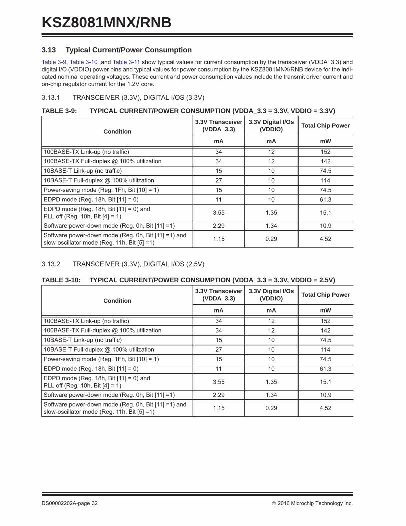
3.13 Typical Current/Power ConsumptionTable 3-9, Table 3-10 ,and Table 3-11 show typical values for current consumption by the transceiver (VDDA_3.3) anddigital I/O (VDDIO) power pins and typical values for power consumption by the KSZ8081MNX/RNB device for the indi-cated nominal operating voltages. These current and power consumption values include the transmit driver current andon-chip regulator current for the 1.2V core.3.13.1 TRANSCEIVER (3.3V), DIGITAL I/OS (3.3V)
3.13.2 TRANSCEIVER (3.3V), DIGITAL I/OS (2.5V)
TABLE 3-10: TYPICAL CURRENT/POWER CONSUMPTION (VDDA_3.3 = 3.3V, VDDIO = 2.5V)
TABLE 3-9: TYPICAL CURRENT/POWER CONSUMPTION (VDDA_3.3 = 3.3V, VDDIO = 3.3V)
Condition3.3V Transceiver
(VDDA_3.3)3.3V Digital I/Os
(VDDIO) Total Chip Power
mA mA mW
100BASE-TX Link-up (no traffic) 34 12 152100BASE-TX Full-duplex @ 100% utilization 34 12 14210BASE-T Link-up (no traffic) 15 10 74.510BASE-T Full-duplex @ 100% utilization 27 10 114Power-saving mode (Reg. 1Fh, Bit [10] = 1) 15 10 74.5EDPD mode (Reg. 18h, Bit [11] = 0) 11 10 61.3EDPD mode (Reg. 18h, Bit [11] = 0) andPLL off (Reg. 10h, Bit [4] = 1) 3.55 1.35 15.1
Software power-down mode (Reg. 0h, Bit [11] =1) 2.29 1.34 10.9Software power-down mode (Reg. 0h, Bit [11] =1) and slow-oscillator mode (Reg. 11h, Bit [5] =1) 1.15 0.29 4.52
DS00002202A-page 32 2016 Microchip Technology Inc.

KSZ8081MNX/RNB
3.13.3 TRANSCEIVER (3.3V), DIGITAL I/OS (1.8V)TABLE 3-11: TYPICAL CURRENT/POWER CONSUMPTION (VDDA_3.3 = 3.3V, VDDIO = 1.8V)
Condition3.3V Transceiver
(VDDA_3.3)1.8V Digital I/Os
(VDDIO) Total Chip Power
mA mA mW
100BASE-TX Link-up (no traffic) 34 11 132100BASE-TX Full-duplex @ 100% utilization 34 12 13410BASE-T Link-up (no traffic) 15 9.0 65.710BASE-T Full-duplex @ 100% utilization 27 9.0 105Power-saving mode (Reg. 1Fh, Bit [10] = 1) 15 9.0 65.7EDPD mode (Reg. 18h, Bit [11] = 0) 11 9.0 52.5EDPD mode (Reg. 18h, Bit [11] = 0) andPLL off (Reg. 10h, Bit [4] = 1) 4.05 1.21 15.5
Software power-down mode (Reg. 0h, Bit [11] =1) 2.79 1.21 11.4Software power-down mode (Reg. 0h, Bit [11] =1) and slow-oscillator mode (Reg. 11h, Bit [5] =1) 1.65 0.19 5.79
2016 Microchip Technology Inc. DS00002202A-page 33

KSZ8081MNX/RNB
4.0 REGISTER DESCRIPTIONS4.1 Register Map
TABLE 4-1: REGISTER MAP
Register Number (Hex) Description
0 Basic Control Register
1h Basic Status
2h PHY Identifier 1
3h PHY Identifier 2
4h Auto-Negotiation Advertisement
5h Auto-Negotiation Link Partner Ability
6h Auto-Negotiation Expansion
7h Auto-Negotiation Next Page
8h Link Partner Next Page Ability
9h Reserved
10h Digital Reserved Control
11h AFE Control 1
12h – 14h Reserved
15h RXER Counter
16h Operation Mode Strap Override
17h Operation Mode Strap Status
18h Expanded Control
19h – 1Ah Reserved
1Bh Interrupt Control/Status
1Ch Reserved
1Dh LinkMD Control/Status
1Eh PHY Control 1
1Fh PHY Control 2
DS00002202A-page 34 2016 Microchip Technology Inc.

KSZ8081MNX/RNB
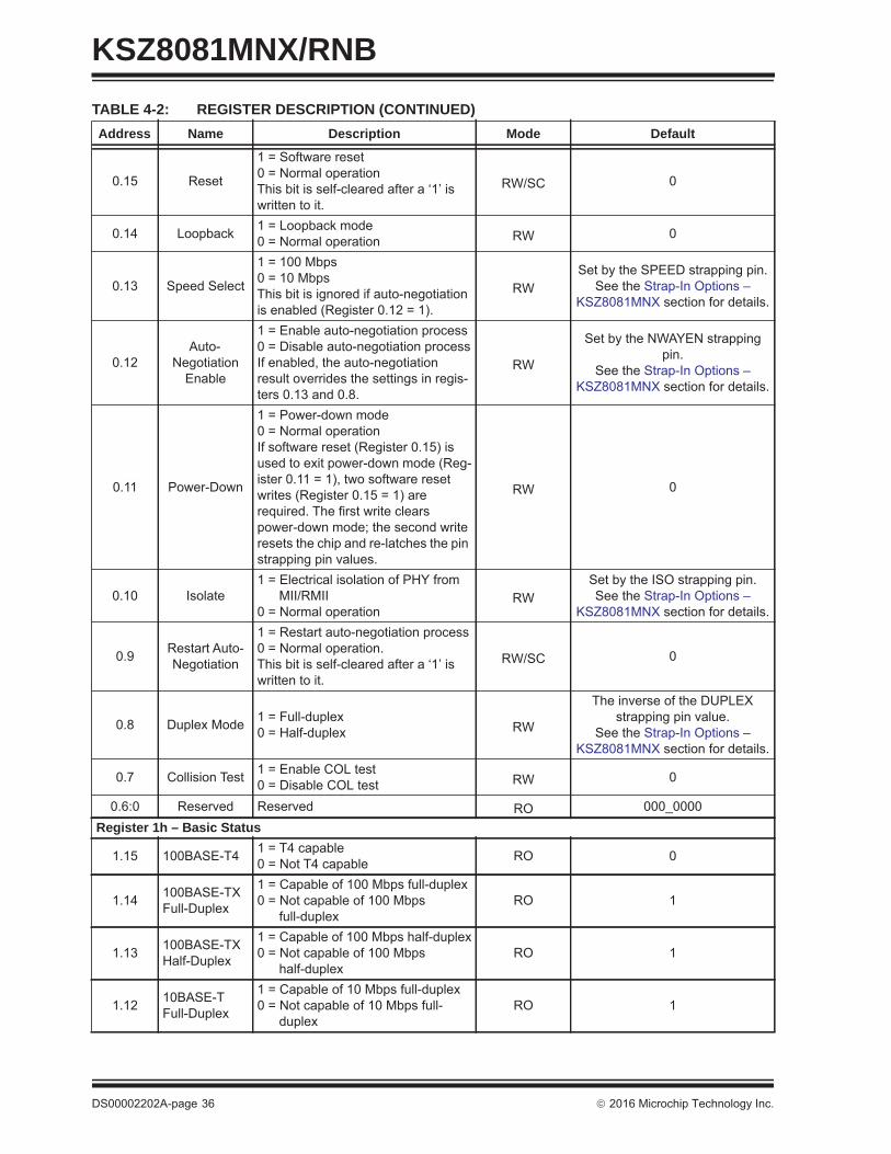
4.2 Register DescriptionTABLE 4-2: REGISTER DESCRIPTION Address Name Description Mode Default
Register 0h – Basic Control
0.15 Reset
1 = Software reset0 = Normal operationThis bit is self-cleared after a ‘1’ is written to it.
RW/SC 0
0.14 Loopback1 = Loopback mode0 = Normal operation
RW 0
0.13 Speed Select
1 = 100 Mbps0 = 10 MbpsThis bit is ignored if auto-negotiation is enabled (Register 0.12 = 1).
RWSet by the SPEED strapping pin.
See the Strap-In Options – KSZ8081MNX section for details.
0.12Auto-
Negotiation Enable
1 = Enable auto-negotiation process
0 = Disable auto-negotiation process
If enabled, the auto-negotiation result overrides the settings in registers 0.13 and 0.8.
RW
Set by the NWAYEN strapping pin.
See the Strap-In Options – KSZ8081MNX section for details.
0.11 Power-Down
1 = Power-down mode0 = Normal operationIf software reset (Register 0.15) is used to exit power-down mode (Register 0.11 = 1), two software reset writes (Register 0.15 = 1) are required. The first write clears power-down mode; the second write resets the chip and re-latches the pin strapping pin values.
RW 0
0.10 Isolate1 = Electrical isolation of PHY from
MII/RMII0 = Normal operation
RWSet by the ISO strapping pin.See the Strap-In Options –
KSZ8081MNX section for details.
0.9 Restart Auto-Negotiation
1 = Restart auto-negotiation process
0 = Normal operation.This bit is self-cleared after a ‘1’ is written to it.
RW/SC 0
0.8 Duplex Mode1 = Full-duplex0 = Half-duplex
RW
The inverse of the DUPLEX strapping pin value.
See the Strap-In Options – KSZ8081MNX section for details.
0.7 Collision Test1 = Enable COL test0 = Disable COL test
RW 0
0.6:0 Reserved Reserved RO 000_0000
2016 Microchip Technology Inc. DS00002202A-page 35
KSZ8081MNX/RNB
0.15 Reset
1 = Software reset0 = Normal operationThis bit is self-cleared after a ‘1’ is written to it.
RW/SC 0
0.14 Loopback 1 = Loopback mode0 = Normal operation RW 0
0.13 Speed Select
1 = 100 Mbps0 = 10 MbpsThis bit is ignored if auto-negotiation is enabled (Register 0.12 = 1).
RWSet by the SPEED strapping pin.
See the Strap-In Options – KSZ8081MNX section for details.
0.12Auto-
NegotiationEnable
1 = Enable auto-negotiation process0 = Disable auto-negotiation processIf enabled, the auto-negotiation result overrides the settings in regis-ters 0.13 and 0.8.
RW
Set by the NWAYEN strapping pin.
See the Strap-In Options – KSZ8081MNX section for details.
0.11 Power-Down
1 = Power-down mode0 = Normal operationIf software reset (Register 0.15) is used to exit power-down mode (Reg-ister 0.11 = 1), two software reset writes (Register 0.15 = 1) are required. The first write clears power-down mode; the second write resets the chip and re-latches the pin strapping pin values.
RW 0
0.10 Isolate1 = Electrical isolation of PHY from
MII/RMII0 = Normal operation
RWSet by the ISO strapping pin.See the Strap-In Options –
KSZ8081MNX section for details.
0.9 Restart Auto-Negotiation
1 = Restart auto-negotiation process0 = Normal operation.This bit is self-cleared after a ‘1’ is written to it.
RW/SC 0
0.8 Duplex Mode 1 = Full-duplex0 = Half-duplex RW
The inverse of the DUPLEX strapping pin value.
See the Strap-In Options – KSZ8081MNX section for details.
0.7 Collision Test 1 = Enable COL test0 = Disable COL test RW 0
0.6:0 Reserved Reserved RO 000_0000Register 1h – Basic Status
1.15 100BASE-T4 1 = T4 capable0 = Not T4 capable RO 0
1.14 100BASE-TX Full-Duplex
1 = Capable of 100 Mbps full-duplex0 = Not capable of 100 Mbps
full-duplexRO 1
1.13 100BASE-TX Half-Duplex
1 = Capable of 100 Mbps half-duplex0 = Not capable of 100 Mbps
half-duplexRO 1
1.12 10BASE-T Full-Duplex
1 = Capable of 10 Mbps full-duplex0 = Not capable of 10 Mbps full-
duplexRO 1
TABLE 4-2: REGISTER DESCRIPTION (CONTINUED)Address Name Description Mode Default
DS00002202A-page 36 2016 Microchip Technology Inc.

KSZ8081MNX/RNB
1.11 10BASE-T Half-Duplex
1 = Capable of 10 Mbps half-duplex0 = Not capable of 10 Mbps half-
duplexRO 1
1.10:7 Reserved Reserved RO 000_0
1.6 No Preamble 1 = Preamble suppression0 = Normal preamble RO 1
1.5 Auto-Negotia-tion Complete
1 = Auto-negotiation process completed
0 = Auto-negotiation process not completed
RO 0
1.4 Remote Fault 1 = Remote fault0 = No remote fault RO/LH 0
1.3 Auto-Negotia-tion Ability
1 = Can perform auto-negotiation0 = Cannot perform auto-negotiation RO 1
1.2 Link Status 1 = Link is up0 = Link is down RO/LL 0
1.1 Jabber Detect1 = Jabber detected0 = Jabber not detected (default is
low)RO/LH 0
1.0 Extended Capability
1 = Supports extended capability registers RO 1
Register 2h – PHY Identifier 1
2.15:0 PHY ID Num-ber
Assigned to the 3rd through 18th bits of the Organizationally Unique Identi-fier (OUI). KENDIN Communication’s OUI is 0010A1 (hex).
RO 0022h
Register 3h – PHY Identifier 2
3.15:10
PHY ID Num-ber
Assigned to the 19th through 24th bits of the Organizationally Unique Identifier (OUI). KENDIN Communi-cation’s OUI is 0010A1 (hex).
RO 0001_01
3.9:4 Model Number Six-bit manufacturer’s model number RO 01_0110
3.3:0Revision Num-ber
Four-bit manufacturer’s revision number RO Rev. A and Rev. A2=0x0.
Rev. A3=0x1Register 4h – Auto-Negotiation Advertisement
4.15 Next Page
1 = Next page capable0 = No next page capabilityNote: Recommended to set this bit to “0”.
RW 0
4.14 Reserved Reserved RO 0
4.13 Remote Fault 1 = Remote fault supported0 = No remote fault RW 0
4.12 Reserved Reserved RO 0
4.11:10 Pause
[00] = No pause[10] = Asymmetric pause[01] = Symmetric pause[11] = Asymmetric and symmetric
pause
RW 00
4.9 100BASE-T4 1 = T4 capable0 = No T4 capability RO 0
TABLE 4-2: REGISTER DESCRIPTION (CONTINUED)Address Name Description Mode Default
2016 Microchip Technology Inc. DS00002202A-page 37

KSZ8081MNX/RNB
4.8 100BASE-TX Full-Duplex
1 = 100 Mbps full-duplex capable0 = No 100 Mbps full-duplex
capabilityRW
Set by the SPEED strapping pin.See the Strap-In Options –
KSZ8081MNX section for details.
4.7 100BASE-TX Half-Duplex
1 = 100 Mbps half-duplex capable0 = No 100 Mbps half-duplex
capabilityRW
Set by the SPEED strapping pin.See the Strap-In Options –
KSZ8081MNX section for details.
4.6 10BASE-T Full-Duplex
1 = 10 Mbps full-duplex capable0 = No 10 Mbps full-duplex capability RW 1
4.5 10BASE-T Half-Duplex
1 = 10 Mbps half-duplex capable0 = No 10 Mbps half-duplex
capabilityRW 1
4.4:0 Selector Field [00001] = IEEE 802.3 RW 0_0001Register 5h – Auto-Negotiation Link Partner Ability
5.15 Next Page 1 = Next page capable0 = No next page capability RO 0
5.14 Acknowledge1 = Link code word received from
partner0 = Link code word not yet received
RO 0
5.13 Remote Fault 1 = Remote fault detected0 = No remote fault RO 0
5.12 Reserved Reserved RO 0
5.11:10 Pause
[00] = No pause[10] = Asymmetric pause[01] = Symmetric pause[11] = Asymmetric and symmetric
pause
RO 00
5.9 100BASE-T4 1 = T4 capable0 = No T4 capability RO 0
5.8 100BASE-TX Full-Duplex
1 = 100 Mbps full-duplex capable0 = No 100 Mbps full-duplex
capabilityRO 0
Register 5h – Auto-Negotiation Link Partner Ability
5.7 100BASE-TX Half-Duplex
1 = 100 Mbps half-duplex capable0 = No 100 Mbps half-duplex
capabilityRO 0
5.6 10BASE-T Full-Duplex
1 = 10 Mbps full-duplex capable0 = No 10 Mbps full-duplex capability RO 0
5.5 10BASE-T Half-Duplex
1 = 10 Mbps half-duplex capable0 = No 10 Mbps half-duplex
capabilityRO 0
5.4:0 Selector Field [00001] = IEEE 802.3 RO 0_0001Register 6h – Auto-Negotiation Expansion
6.15:5 Reserved Reserved RO 0000_0000_000
6.4 Parallel Detec-tion Fault
1 = Fault detected by parallel detection0 = No fault detected by parallel detection
RO/LH 0
6.3Link Partner Next Page
Able
1 = Link partner has next page capability0 = Link partner does not have next page capability
RO 0
TABLE 4-2: REGISTER DESCRIPTION (CONTINUED)Address Name Description Mode Default
DS00002202A-page 38 2016 Microchip Technology Inc.

KSZ8081MNX/RNB
6.2 Next Page Able
1 = Local device has next page capability0 = Local device does not have next page capability
RO 1
6.1 Page Received
1 = New page received0 = New page not received yet RO/LH 0
6.0Link Partner
Auto-Negotia-tion Able
1 = Link partner has auto-negotiation capability0 = Link partner does not have auto-negotiation capability
RO 0
Register 7h – Auto-Negotiation Next Page
7.15 Next Page 1 = Additional next pages will follow0 = Last page RW 0
7.14 Reserved Reserved RO 0
7.13 Message Page
1 = Message page0 = Unformatted page RW 1
7.12 Acknowledge2
1 = Will comply with message0 = Cannot comply with message RW 0
7.11 Toggle1 = Previous value of the transmitted link code word equaled logic 10 = Logic 0
RO 0
7.10:0 Message Field
11-bit wide field to encode 2048 messages RW 000_0000_0001
Register 8h – Link Partner Next Page Ability
8.15 Next Page 1 = Additional next pages will follow0 = Last page RO 0
8.14 Acknowledge 1 = Successful receipt of link word0 = No successful receipt of link word RO 0
8.13 Message Page
1 = Message page0 = Unformatted page RO 0
8.12 Acknowledge2 1 = Can act on the information0 = Cannot act on the information RO 0
8.11 Toggle
1 = Previous value of transmitted link code word equal to logic 00 = Previous value of transmitted link code word equal to logic 1
RO 0
8.10:0 Message Field 11-bit wide field to encode 2048 messages RO 000_0000_0000
Register 10h – Digital Reserved Control10.15:5 Reserved Reserved RW 0000_0000_000
10.4 PLL Off
1 = Turn PLL off automatically in EDPD mode0 = Keep PLL on in EDPD mode.See also Register 18h, Bit [11] for EDPD mode
RW 0
10.3:0 Reserved Reserved RW 0000Register 11h – AFE Control 1
11.15:6 Reserved Reserved RW 0000_0000_00
TABLE 4-2: REGISTER DESCRIPTION (CONTINUED)Address Name Description Mode Default
2016 Microchip Technology Inc. DS00002202A-page 39

KSZ8081MNX/RNB
11.5Slow-Oscilla-
tor Mode Enable
Slow-oscillator mode is used to disconnect the input reference crystal/clock on the XI pin and select the on-chip slow oscillator when the KSZ8081MNX/RNB device is not in use after power-up.1 = Enable0 = DisableThis bit automatically sets software power-down to the analog side when enabled.
RW 0
11.4:0 Reserved Reserved RW 0_0000Register 15h – RXER Counter
15.15:0 RXER Counter
Receive error counter for symbol error frames RO/SC 0000h
Register 16h – Operation Mode Strap Override
16.15 ReservedFactory Mode
0 = Normal operation1 = Factory test modeIf TXC (Pin 22) latches in a pull-up value at the de-assertion of reset, write a ‘0’ to this bit to clear Reserved Factory Mode.This bit applies only to KSZ8081MNX.
RW0
Set by the pull-up/pull-down value of TXC (Pin 22).
16.14:11 Reserved Reserved RW 000_016.10 Reserved Reserved RO 0
16.9 B-CAST_OFF Override
1 = Override strap-in for B-CAST_OFFIf bit is ‘1’, PHY Address 0 is non-broadcast.
RW 0
16.8 Reserved Reserved RW 0
16.7 MII B-to-B Override
1 = Override strap-in for MII back-to-back mode (also set Bit 0 of this reg-ister to ‘1’)This bit applies only to KSZ8081MNX.
RW 0
16.6 RMII B-to-B Override
1 = Override strap-in for RMII Back-to-Back mode (also set Bit 1 of this register to ‘1’)This bit applies only to KSZ8081RNB.
RW 0
16.5 NAND Tree Override
1 = Override strap-in for NAND tree mode RW 0
16.4:2 Reserved Reserved RW 0_00
16.1 RMII Override1 = Override strap-in for RMII modeThis bit applies only to KSZ8081RNB.
RW 0
16.0 MII Override1 = Override strap-in for MII modeThis bit applies only to KSZ8081MNX.
RW 1
TABLE 4-2: REGISTER DESCRIPTION (CONTINUED)Address Name Description Mode Default
DS00002202A-page 40 2016 Microchip Technology Inc.

KSZ8081MNX/RNB
Register 17h – Operation Mode Strap Status
17.15:13 PHYAD[2:0] Strap-In Status
[000] = Strap to PHY Address 0[001] = Strap to PHY Address 1[010] = Strap to PHY Address 2[011] = Strap to PHY Address 3[100] = Strap to PHY Address 4[101] = Strap to PHY Address 5[110] = Strap to PHY Address 6[111] = Strap to PHY Address 7
RO —
17.12:10 Reserved Reserved RO —
17.9 B-CAST_OFF Strap-In Status
1 = Strap to B-CAST_OFFIf bit is ‘1’, PHY Address 0 is non-broadcast.
RO —
17.8 Reserved Reserved RO —
17.7 MII B-to-B Strap-In Status
1 = Strap to MII back-to-back modeThis bit applies only to KSZ8081MNX.
RO —
17.6 RMII B-to-B Strap-In Status
1 = Strap to RMII Back-to-Back modeThis bit applies only to KSZ8081RNB.
RO —
17.5 NAND Tree Strap-In Status 1 = Strap to NAND tree mode RO —
17.4:2 Reserved Reserved RO —
17.1 RMII Strap-In Status
1 = Strap to RMII modeThis bit applies only to KSZ8081RNB.
RO —
17.0 MII Strap-In Status
1 = Strap to MII modeThis bit applies only to KSZ8081MNX.
RO —
Register 18h – Expanded Control18.15:12 Reserved Reserved RW 0000
18.11 EDPD Disabled
Energy-detect power-down mode1 = Disable0 = EnableSee also Register 10h, Bit [4] for PLL off.
RW 1
18.10 100BASE-TX Latency
1 = MII output is random latency0 = MII output is fixed latencyFor both settings, all bytes of received preamble are passed to the MII output.This bit applies only to KSZ8081MNX.
RW 0
18.9:7 Reserved Reserved RW 00_0
18.610BASE-T Preamble Restore
1 = Restore received preamble to MII output0 = Remove all seven bytes of pre-amble before sending frame (starting with SFD) to MII outputThis bit applies only to KSZ8081MNX,
RW 0
TABLE 4-2: REGISTER DESCRIPTION (CONTINUED)Address Name Description Mode Default
2016 Microchip Technology Inc. DS00002202A-page 41

KSZ8081MNX/RNB
18.5:0 Reserved Reserved RW 00_0000Register 1Bh – Interrupt Control/Status
1B.15Jabber
Interrupt Enable
1 = Enable jabber interrupt0 = Disable jabber interrupt RW 0
1B.14Receive Error
Interrupt Enable
1 = Enable receive error interrupt0 = Disable receive error interrupt RW 0
1B.13
Page Received Interrupt Enable
1 = Enable page received interrupt0 = Disable page received interrupt RW 0
1B.12Parallel Detect Fault Interrupt
Enable
1 = Enable parallel detect fault inter-rupt0 = Disable parallel detect fault inter-rupt
RW 0
1B.11
Link Partner Acknowledge
Interrupt Enable
1 = Enable link partner acknowledge interrupt0 = Disable link partner acknowledge interrupt
RW 0
1B.10Link-Down Interrupt Enable
1= Enable link-down interrupt0 = Disable link-down interrupt RW 0
1B.9Remote Fault
Interrupt Enable
1 = Enable remote fault interrupt0 = Disable remote fault interrupt RW 0
1B.8Link-Up Interrupt Enable
1 = Enable link-up interrupt0 = Disable link-up interrupt RW 0
1B.7 Jabber Interrupt
1 = Jabber occurred0 = Jabber did not occur RO/SC 0
1B.6 Receive Error Interrupt
1 = Receive error occurred0 = Receive error did not occur RO/SC 0
1B.5 Page Receive Interrupt
1 = Page receive occurred0 = Page receive did not occur RO/SC 0
1B.4 Parallel Detect Fault Interrupt
1 = Parallel detect fault occurred0 = Parallel detect fault did not occur RO/SC 0
1B.3Link Partner
Acknowledge Interrupt
1 = Link partner acknowledge occurred0 = Link partner acknowledge did not occur
RO/SC 0
1B.2 Link-Down Interrupt
1 = Link-down occurred0 = Link-down did not occur RO/SC 0
1B.1 Remote Fault Interrupt
1 = Remote fault occurred0 = Remote fault did not occur RO/SC 0
1B.0 Link-Up Interrupt
1 = Link-up occurred0 = Link-up did not occur RO/SC 0
TABLE 4-2: REGISTER DESCRIPTION (CONTINUED)Address Name Description Mode Default
DS00002202A-page 42 2016 Microchip Technology Inc.

KSZ8081MNX/RNB
Register 1Dh – LinkMD Control/Status
1D.15Cable Diag-nostic Test
Enable
1 = Enable cable diagnostic test. After test has completed, this bit is self-cleared.0 = Indicates cable diagnostic test (if enabled) has completed and the sta-tus information is valid for read.
RW/SC 0
1D.14:13Cable Diag-nostic Test
Result
[00] = Normal condition[01] = Open condition has been detected in cable[10] = Short condition has been detected in cable[11] = Cable diagnostic test has failed
RO 00
1D.12 Short Cable Indicator
1 = Short cable (<10 meter) has been detected by LinkMD RO 0
1D.11:9 Reserved Reserved RW 000
1D.8:0 Cable Fault Counter Distance to fault RO 0_0000_0000
Register 1Eh – PHY Control 1
1E.15:10 Reserved Reserved RO 0000_00
1E.9Enable
Pause (Flow Control)
1 = Flow control capable0 = No flow control capability
RO 0
1E.8 Link Status1 = Link is up0 = Link is down
RO 0
1E.7 Polarity Status
1 = Polarity is reversed0 = Polarity is not reversed
RO
1E.6 Reserved Reserved RO 0
1E.5 MDI/MDI-X State
1 = MDI-X0 = MDI
RO
1E.4 Energy Detect
1 = Signal present on receive differential pair0 = No signal detected on receive differential pair
RO 0
1E.3 PHY Isolate1 = PHY in isolate mode0 = PHY in normal operation
RW 0
1E.2:0Operation
Mode Indication
[000] = Still in auto-negotiation[001] = 10BASE-T half-duplex[010] = 100BASE-TX half-duplex[011] = Reserved[100] = Reserved[101] = 10BASE-T full-duplex[110] = 100BASE-TX full-duplex[111] = Reserved
RO 000
TABLE 4-2: REGISTER DESCRIPTION (CONTINUED)Address Name Description Mode Default
2016 Microchip Technology Inc. DS00002202A-page 43

KSZ8081MNX/RNB
Register 1Fh – PHY Control 2
1F.15 HP_MDIX 1 = HP Auto MDI/MDI-X mode0 = Auto MDI/MDI-X mode RW 1
1F.14 MDI/MDI-X Select
When Auto MDI/MDI-X is disabled,1 = MDI-X modeTransmit on RXP,RXM (pins 5, 4) andReceive on TXP,TXM (pins 7, 6)0 = MDI modeTransmit on TXP,TXM (pins 7, 6) andReceive on RXP,RXM (pins 5, 4)
RW 0
1F.13 Pair Swap Disable
1 = Disable Auto MDI/MDI-X0 = Enable Auto MDI/MDI-X RW 0
1F.12 Reserved Reserved RW 0
1F.11 Force Link
1 = Force link pass0 = Normal link operationThis bit bypasses the control logic and allows the transmitter to send a pattern even if there is no link.
RW 0
1F.10 Power Saving 1 = Enable power saving 0 = Disable power saving RW 0
1F.9 Interrupt Level 1 = Interrupt pin active high0 = Interrupt pin active low RW 0
1F.8 Enable Jabber 1 = Enable jabber counter0 = Disable jabber counter RW 1
1F.7RMII Refer-ence Clock
Select
1 = RMII 50 MHz clock mode; clock input to XI (Pin 9) is 50 MHz 0 = RMII 25 MHz clock mode; clock input to XI (Pin 9) is 25 MHzThis bit applies only to KSZ8081RNB.
RW 0
1F.6 Reserved Reserved RW 0
1F.5:4 LED Mode
[00] =LED1: SpeedLED0: Link/Activity[01] = LED1: ActivityLED0: Link[10], [11] = Reserved
RW 00
1F.3 Disable Transmitter
1 = Disable transmitter0 = Enable transmitter RW 0
1F.2 Remote Loopback
1 = Remote (analog) loopback is enabled0 = Normal mode
RW 0
1F.1 Enable SQE Test
1 = Enable SQE test0 = Disable SQE test RW 0
1F.0 Disable Data Scrambling
1 = Disable scrambler0 = Enable scrambler RW 0
TABLE 4-2: REGISTER DESCRIPTION (CONTINUED)Address Name Description Mode Default
DS00002202A-page 44 2016 Microchip Technology Inc.

KSZ8081MNX/RNB
5.0 OPERATIONAL CHARACTERISTICS5.1 Absolute Maximum Ratings*Supply Voltage (VIN)(VDD_1.2).................................................................................................................................................... –0.5V to +1.8V(VDDIO, VDDA_3.3) ...................................................................................................................................... –0.5V to +5.0V
Input Voltage (all inputs)............................................................................................................................ –0.5V to +5.0V
Output Voltage (all outputs)....................................................................................................................... –0.5V to +5.0V
Lead Temperature (soldering, 10s) ......................................................................................................................... 260°C
Storage Temperature (TS) ......................................................................................................................–55°C to +150°C
* Exceeding the absolute maximum ratings can damage the device. Stresses greater than the absolute maximum ratingcan cause permanent damage to the device. Operation of the device at these or any other conditions abovethose specified in the operating sections of this specification is not implied. Maximum conditions for extendedperiods may affect reliability.
5.2 Operating Ratings**Supply Voltage(VDDIO_3.3, VDDA_3.3) ........................................................................................................................ +3.135V to +3.465V(VDDIO_2.5)......................................................................................................................................... +2.375V to +2.625V(VDDIO_1.8)......................................................................................................................................... +1.710V to +1.890V
Ambient Temperature(TA, Commercial)..........................................................................................................................................0°C to +70°C(TA, Industrial) ..........................................................................................................................................–40°C to +85°CMaximum Junction Temperature (TJ max.) ...........................................................................................................+125°CThermal Resistance (TJA) ............................................................................................................................... 45.87°C/WThermal Resistance (TJC) ............................................................................................................................... 15.85°C/W** The device is not guaranteed to function outside its operating ratings.
2016 Microchip Technology Inc. DS00002202A-page 45

KSZ8081MNX/RNB
6.0 ELECTRICAL CHARACTERISTICSSymbol Parameter Condition Min. Typ. Max. Units
Supply Current (VDDIO, VDDA_3.3 = 3.3V)
IDD1_3.3V 10BASE-T Full-duplex traffic @ 100% utilization
— 41 — mA
IDD2_3.3V 100BASE-TX Full-duplex traffic @ 100% utilization
— 47 — mA
IDD3_3.3V EDPD Mode Ethernet cable disconnected (reg. 18h.11 = 0)
— 20 — mA
IDD4_3.3V Power-Down Mode Software power-down (reg. 0h.11 = 1)
— 4 — mA
CMOS Level Inputs
VIH Input High VoltageVDDIO = 3.3V 2.0 — —
VVDDIO = 2.5V 1.8 — —VDDIO = 1.8V 1.3 — —
VIL Input Low VoltageVDDIO = 3.3V — — 0.8
VVDDIO = 2.5V — — 0.7VDDIO = 1.8V — — 0.5
|IIN| Input Current VIN = GND ~ VDDIO — — 10 μACMOS Level Outputs
VOH Output High VoltageVDDIO = 3.3V 2.4 — —
VVDDIO = 2.5V 2.0 — —VDDIO = 1.8V 1.5 — —
VOL Output Low VoltageVDDIO = 3.3V — — 0.4
VVDDIO = 2.5V — — 0.4VDDIO = 1.8V — — 0.3
|Ioz| Output Tri-State Leakage — — — 10 μALED OutputILED Output Drive Current Each LED pin (LED0, LED1) — 8 — mAAll Pull-Up/Pull-Down Pins (including Strapping Pins)
pu Internal Pull-Up Resistance
VDDIO = 3.3V 30 45 73
kΩVDDIO = 2.5V 39 61 102
VDDIO = 1.8V 48 99 178
pd Internal Pull-Down Resistance
VDDIO = 3.3V 26 43 79
kΩVDDIO = 2.5V 34 59 113
VDDIO = 1.8V 53 99 200100BASE-TX Transmit (measured differentially after 1:1 transformer)
VOPeak Differential Output Volt-age
100Ω termination across dif-ferential output 0.95 — 1.05 V
VIMB Output Voltage Imbalance 100Ω termination across dif-ferential output — — 2 %
tr, tf Rise/Fall Time — 3 — 5 ns— Rise/Fall Time Imbalance — 0 — 0.5 ns— Duty Cycle Distortion — — — ±0.25 ns— Overshoot — — — 5 %— Output Jitter Peak-to-peak — 0.7 — ns
DS00002202A-page 46 2016 Microchip Technology Inc.

KSZ8081MNX/RNB
10BASE-T Transmit (measured differentially after 1:1 transformer)
VPPeak Differential Output Volt-age
100Ω termination across dif-ferential output 2.2 — 2.8 V
Jitter Added Peak-to-peak — — 3.5 nstr, tf Rise/Fall Time — — 25 — ns10BASE-T ReceiveVSQ Squelch Threshold 5 MHz square wave — 400 — mVTransmitter – Drive SettingVSET Reference Voltage of ISET R(ISET) = 6.49 kΩ — 0.65 — VREF_CLK Output
— 50 MHz RMII Clock Output Jitter
Peak-to-peak. (Applies only to KSZ8081RNB in RMII – 25 MHz clock mode)
— 300 — ps
100 Mbps Mode – Industrial Applications Parameters
— Clock Phase Delay – XI Input to MII TXC Output
XI (25 MHz clock input) to MII TXC (25 MHz clock output) delay, referenced to rising edges of both clocks. (Applies only to KSZ8081MNX in MII mode)
15 20 25 ns
tllrLink Loss Reaction (Indication) Time
Link loss detected at receive differential inputs to PHY sig-nal indication time for each of the following:1. For LED mode 00, Speed LED output changes from low (100 Mbps) to high (10 Mbps, default state for link-down).2. For LED mode 01, Link LED output changes from low (link-up) to high (link-down).3. INTRP pin asserts for link-down status change.
— 4.4 — μs
Symbol Parameter Condition Min. Typ. Max. Units
2016 Microchip Technology Inc. DS00002202A-page 47

KSZ8081MNX/RNB
7.0 TIMING DIAGRAMS7.1 MII SQE Timing (10BASE-T)
FIGURE 7-1: MII SQE TIMING (10BASE-T)
7.2 MII Transmit Timing (10BASE-T)
FIGURE 7-2: MII TRANSMIT TIMING (10BASE-T)
TABLE 7-1: MII SQE TIMING (10BASE-T) PARAMETERSTiming Parameters Description Min. Typ. Max. Units
tP TXC period — 400 — nstWL TXC pulse width low — 200 — nstWH TXC pulse width high — 200 — ns
tSQECOL (SQE) delay after TXEN de-asserted
— 2.2 — μs
tSQEP COL (SQE) pulse duration — 1.0 — μs
TABLE 7-2: MII TRANSMIT TIMING (10BASE-T) PARAMETERSTiming Parameters Description Min. Typ. Max. Units
tP TXC period — 400 — nstWL TXC pulse width low — 200 — nstWH TXC pulse width high — 200 — nstSU1 TXD[3:0] setup to rising edge of TXC 120 — — nstSU2 TXEN setup to rising edge of TXC 120 — — ns
tWL
tWH
tP
tSQE
tSQEP
TXC
TXEN
COL
CRS
TXEN
TXD[3:0]
TXC
tCRS1
tWL
tP
tHD2
tCRS2
tWH
tHD1
tSU2
tSU1
DS00002202A-page 48 2016 Microchip Technology Inc.

KSZ8081MNX/RNB
7.3 MII Receive Timing (10BASE-T)
FIGURE 7-3: MII RECEIVE TIMING (10BASE-T)
tHD1 TXD[3:0] hold from rising edge of TXC 0 — — nstHD2 TXEN hold from rising edge of TXC 0 — — nstCRS1 TXEN high to CRS asserted latency 600 — nstCRS2 TXEN low to CRS de-asserted latency 1.0 — μs
TABLE 7-3: MII RECEIVE TIMING (10BASE-T) PARAMETERSTiming Parameters Description Min. Typ. Max. Units
tP RXC period — 400 — nstWL RXC pulse width low — 200 — nstWH RXC pulse width high — 200 — ns
tOD(RXDV, RXD[3:0], RXER) output delay from rising edge of RXC
— 205 — ns
tRLAT CRS to (RXDV, RXD[3:0]) latency — 7.2 — μs
TABLE 7-2: MII TRANSMIT TIMING (10BASE-T) PARAMETERSTiming Parameters Description Min. Typ. Max. Units
CRS
RXDV
RXD[3:0]RXER
RXC
tRLAT
tOD
tP
tWL
tWH
2016 Microchip Technology Inc. DS00002202A-page 49
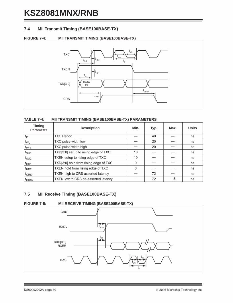
KSZ8081MNX/RNB
7.4 MII Transmit Timing (BASE100BASE-TX)FIGURE 7-4: MII TRANSMIT TIMING (BASE100BASE-TX)
7.5 MII Receive Timing (BASE100BASE-TX)
FIGURE 7-5: MII RECEIVE TIMING (BASE100BASE-TX)
TABLE 7-4: MII TRANSMIT TIMING (BASE100BASE-TX) PARAMETERSTiming
Parameter Description Min. Typ. Max. Units
tP TXC Period — 40 — nstWL TXC pulse width low — 20 — nstWH TXC pulse width high — 20 — nstSU1 TXD[3:0] setup to rising edge of TXC 10 — — nstSU2 TXEN setup to rising edge of TXC 10 — — nstHD1 TXD[3:0] hold from rising edge of TXC 0 — — nstHD2 TXEN hold from rising edge of TXC 0 — — nstCRS1 TXEN high to CRS asserted latency — 72 — nstCRS2 TXEN low to CRS de-asserted latency — 72 —S ns
CRS
TXEN
TXD[3:0]
TXC
tCRS1
tWL
tP
tHD1tSU1
tCRS2
DATAIN
tWHtHD2tSU2
CRS
RXDV
RXD[3:0]RXER
RXC
tOD
tP
tWL
tWH
tRLAT
DS00002202A-page 50 2016 Microchip Technology Inc.

KSZ8081MNX/RNB
7.6 RMII Timing
FIGURE 7-6: RMII TIMING – DATA RECEIVED FROM RMII
FIGURE 7-7: RMII TIMING – DATA INPUT TO RMII
TABLE 7-5: MII RECEIVE TIMING (BASE100BASE-TX) PARAMETERSTiming
Parameter Description Min. Typ. Max. Units
tP RXC period — 40 — nstWL RXC pulse width low — 20 — nstWH RXC pulse width high — 20 — nstOD (RXDV, RXD[3:0], RXER) output delay from ris-
ing edge of RXC 16 21 25 ns
tFLAT CRS to (RXDV, RXD[3:0] latency — 170 — ns
tCYC
REF_CLK
TXENTXD[1:0]
t1
t2
TRANSMIT TIMING
tCYC
REF_CLK
CRS_DVRXD[1:0]
RXER
tOD
RECEIVETIMING
2016 Microchip Technology Inc. DS00002202A-page 51

KSZ8081MNX/RNB
7.7 Auto-Negotiation Timing
FIGURE 7-8: AUTO-NEGOTIATION TIMING
TABLE 7-6: RMII TIMING PARAMETERS – KSZ8081RNB (25 MHZ INPUT TO XI PIN, 50 MHZ OUTPUT FROM REF_CLK PIN)
Timing Parameter Description Min. Typ. Max Units
tCYC Clock cycle — 20 — nst1 Setup time 4 — — nst2 Hold time 2 — — nstOD Output delay 7 10 13 ns
TABLE 7-7: RMII TIMING PARAMETERS – KSZ8081RNB (25 MHZ INPUT TO XI PIN)Timing Parameter Description Min. Typ. Max Units
tCYC Clock cycle — 20 — nst1 Setup time 4 — — nst2 Hold time 2 — — nstOD Output delay 8 11 13 ns
AUTO -NEGOTIATIONFAST LINK PULSE (FLP) TIMING
tPW
TX+/TX-
CLOCKPULSE
DATAPULSE
CLOCKPULSE
tPW
tCTD
tCTC
tFLPW
tBTB
TX+/TX-
DATAPULSE
FLP BURST
FLP BURST
DS00002202A-page 52 2016 Microchip Technology Inc.

KSZ8081MNX/RNB
7.8 MDC/MDIO Timing
FIGURE 7-9: MDC/MDIO TIMING
TABLE 7-8: AUTO-NEGOTIATION FAST LINK PULSE (FLP) TIMING PARAMETERSTiming Parameter Description Min. Typ. Max. Units
tBTB FLP burst to FLP burst 8 16 24 mstFLPW FLP burst width — 2 — mstPW Clock/Data pulse width — 100 — nstCTD Clock pulse to data pulse 55.5 64 69.5 μstCTC Clock pulse to clock pulse 111 128 139 μs
— Number of clock/data pulses per FLP burst 17 — 33 —
TABLE 7-9: MDC/MDIO TIMING PARAMETERSTiming
Parameter Description Min. Typ. Max. Units
fc MDC Clock Frequency — 2.5 10 MHztP MDC period — 400 — ns
tMD1 MDIO (PHY input) setup to rising edge of MDC 10 — — nstMD2 MDIO (PHY input) hold from rising edge of MDC 4 — — nstMD3 MDIO (PHY output) delay from rising edge of MDC 5 222 — ns
tMD1
VALIDDATA
MDIO(PHY INPUT)
VALIDDATA
MDC
tMD2
MDIO(PHY OUTPUT)
VALIDDATA
tMD3
tP
2016 Microchip Technology Inc. DS00002202A-page 53

KSZ8081MNX/RNB
7.9 Power-up/Reset TimingThe KSZ8081MNX/RNB reset timing requirement is summarized in Figure 7-10 and Table 7-10.FIGURE 7-10: POWER-UP/RESET TIMING
The supply voltage (VDDIO and VDDA_3.3) power-up waveform should be monotonic. The 300 μs minimum rise time isfrom 10% to 90%.
For warm reset, the reset (RST#) pin should be asserted low for a minimum of 500 μs. The strap-in pin values are readand updated at the de-assertion of reset.
After the de-assertion of reset, wait a minimum of 100 μs before starting programming on the MIIM (MDC/MDIO) inter-face.
TABLE 7-10: POWER-UP/RESET TIMING PARAMETERSParameter Description Min. Max. Units
tVR Supply voltage (VDDIO, VDDA_3.3) rise time 300 — μs
tSRStable supply voltage (VDDIO, VDDA_3.3) to reset high 10 — ms
tCS Configuration setup time 5 — nstCH Configuration hold time 5 — nstRC Reset to strap-in pin output 6 — ns
SUPPLYVOLTAGES
RST#
STRAP-INVALUE
STRAP-IN /OUTPUT PIN
tVRtSR
tCS tCH
tRC
DS00002202A-page 54 2016 Microchip Technology Inc.

KSZ8081MNX/RNB
7.10 Reset CircuitFigure 7-11 shows a reset circuit recommended for powering up the KSZ8081MNX/RNB if reset is triggered by thepower supply.FIGURE 7-11: RECOMMENDED RESET CIRCUIT
Figure 7-12 Shows a reset circuit recommended for applications where reset is driven by another device (for example,the CPU or an FPGA). The reset out RST_OUT_n from CPU/FPGA provides the warm reset after power up reset. D2is used if using different VDDIO between the switch and CPU/FPGA, otherwise, the different VDDIO will fight each other.If different VDDIO have to use in a special case, a low VF (<0.3V) diode is required (For example, VISHAY’s BAT54,MSS1P2L and so on), or a level shifter device can be used too. If Ethernet device and CPU/FPGA use same VDDIOvoltage, D2 can be removed to connect both devices directly. Usually, Ethernet device and CPU/FPGA should use sameVDDIO voltage.
FIGURE 7-12: RECOMMENDED RESET CIRCUIT FOR INTERFACING WITH CPU/FPGA RESET OUTPUT
VDDIO
D1: 1N4148
D1 R 10KKSZ8081MNX/RNB
RST#
C 10μF
VDDIO
KSZ8081MNX/RNBD1
R 10K
RST#
C 10μFD2
CPU/FPGA
RST_OUT_N
D1, D2: 1N4148
2016 Microchip Technology Inc. DS00002202A-page 55

KSZ8081MNX/RNB
7.11 Reference Circuits – LED Strap-In PinsThe pull-up, float, and pull-down reference circuits for the LED1/SPEED and LED0/NWAYEN strapping pins are shownin Figure 7-13 for 3.3V and 2.5V VDDIO.FIGURE 7-13: REFERENCE CIRCUITS FOR LED STRAPPING PINS
For using 1.8V VDDIO, should select parts with low 1.8V operation voltage and forwarding current IF about 2 mA LEDindicator. It is okay to use internal pull-up or external pull-up resistor for the LED pin pull-up strap function, and use anexternal 0.75 kΩ to 1 kΩ pull-down resistor for the LED pin pull-down strap function.
Note: If using RJ45 jacks with integrated LEDs and 1.8V VDDIO, a level shifting is required from LED 3.3V to 1.8V. Forexample, use a bipolar transistor or a level shift device.
LED PIN
220Ω4.7kΩPULL_UP
KSZ8081MNX/RXB
VDDIO = 3.3V, 2.5V
LED PIN
220ΩFLOAT
KSZ8081MNX/RXB
VDDIO = 3.3V, 2.5V
LED PIN
220ΩPULL-DOWN
KSZ8081MNX/RXB
VDDIO = 3.3V, 2.5V
1kΩ
DS00002202A-page 56 2016 Microchip Technology Inc.

KSZ8081MNX/RNB
7.12 Reference Clock – Connection and SelectionA crystal or external clock source, such as an oscillator, is used to provide the reference clock for the KSZ8081MNX/RNB. For the KSZ8081MNX in all operating modes and for the KSZ8081RNB in RMII – 25 MHz Clock Mode, the refer-ence clock is 25 MHz. The reference clock connections to XI (Pin 9) and XO (Pin 8), and the reference clock selectioncriteria, are provided in Figure 7-14 and Table 7-11.FIGURE 7-14: 25 MHZ CRYSTAL/OSCILLATOR REFERENCE CLOCK CONNECTION
Note 7-1 ±60 ppm for overtemperature crystal.
For the KSZ8081RNB in RMII – 50 MHz clock mode, the reference clock is 50 MHz. The reference clock connectionsto XI (Pin 9), and the reference clock selection criteria are provided in Figure 7-15 and Table 7-12.
FIGURE 7-15: 50 MHZ OSCILLATOR REFERENCE CLOCK CONNECTION
TABLE 7-11: 25 MHZ CRYSTAL/REFERENCE CLOCK SELECTION CRITERIACharacteristics Value Units
Frequency 25 MHzFrequency tolerance (max) (Note 7-1) ±50 ppmCrystal series resistance (typ) 40 ΩCrystal load capacitance (typ) 22 pF
TABLE 7-12: 50 MHZ OSCILLATOR/REFERENCE CLOCK SELECTION CRITERIACharacteristics Value Units
Frequency 50 MHzFrequency tolerance (maximum) ±50 ppm
NC
XI
XO
25MHz OSC±50PPM
XI
XO
25MHz XTAL±50PPM
22pF
22pF
NC
XI
XO
50MHz OSC±50PPM
2016 Microchip Technology Inc. DS00002202A-page 57
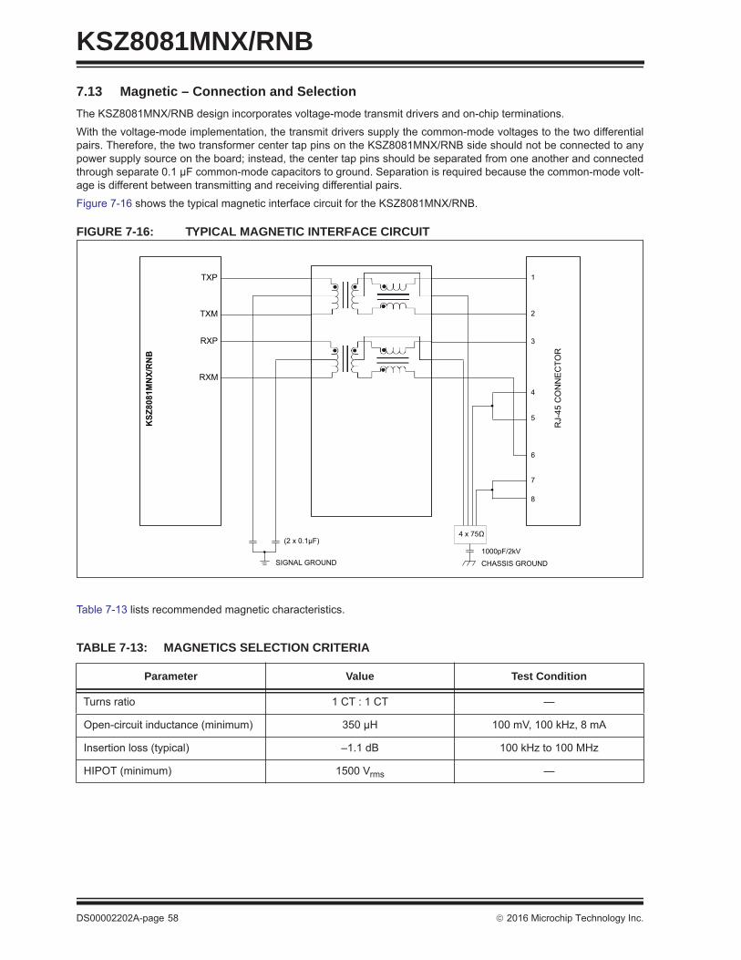
KSZ8081MNX/RNB
7.13 Magnetic – Connection and SelectionThe KSZ8081MNX/RNB design incorporates voltage-mode transmit drivers and on-chip terminations.With the voltage-mode implementation, the transmit drivers supply the common-mode voltages to the two differentialpairs. Therefore, the two transformer center tap pins on the KSZ8081MNX/RNB side should not be connected to anypower supply source on the board; instead, the center tap pins should be separated from one another and connectedthrough separate 0.1 μF common-mode capacitors to ground. Separation is required because the common-mode volt-age is different between transmitting and receiving differential pairs.
Figure 7-16 shows the typical magnetic interface circuit for the KSZ8081MNX/RNB.
FIGURE 7-16: TYPICAL MAGNETIC INTERFACE CIRCUIT
Table 7-13 lists recommended magnetic characteristics.
TABLE 7-13: MAGNETICS SELECTION CRITERIA
Parameter Value Test Condition
Turns ratio 1 CT : 1 CT —
Open-circuit inductance (minimum) 350 μH 100 mV, 100 kHz, 8 mA
Insertion loss (typical) –1.1 dB 100 kHz to 100 MHz
HIPOT (minimum) 1500 Vrms —
1
2
3
7
8
4
5
6
4 x 75Ω
1000pF/2kV R
J-45
CO
NN
EC
TOR
CHASSIS GROUND
(2 x 0.1μF)
TXP
TXM
RXP
RXM
KSZ
8081
MN
X/R
NB
SIGNAL GROUND
DS00002202A-page 58 2016 Microchip Technology Inc.

KSZ8081MNX/RNB
Table 7-14 is a list of compatible single-port magnetics with separated transformer center tap pins on the PHY chip sidethat can be used with the KSZ8081MNX/RNB.TABLE 7-14: COMPATIBLE SINGLE-PORT 10/100 MAGNETICSManufacturer Part Number Temperature Range Magnetic + RJ-45
Bel Fuse S558-5999-U7 0°C to 70°C NoBel Fuse SI-46001-F 0°C to 70°C YesBel Fuse SI-50170-F 0°C to 70°C YesDelta LF8505 0°C to 70°C NoHALO HFJ11-2450E 0°C to 70°C YesHALO TG110-E055N5 –40°C to 85°C NoLANKom LF-H41S-1 0°C to 70°C NoPulse H1102 0°C to 70°C NoPulse H1260 0°C to 70°C NoPulse HX1188 –40°C to 85°C NoPulse J00-0014 0°C to 70°C YesPulse JX0011D21NL –40°C to 85°C YesTDK TLA-6T718A 0°C to 70°C YesTranspower HB726 0°C to 70°C NoWurth/Midcom 000-7090-37R-LF1 –40°C to 85°C No
2016 Microchip Technology Inc. DS00002202A-page 59

KSZ8081MNX/RNB
DS00002202A-page 60 2016 Microchip Technology Inc.
8.0 PACKAGE OUTLINE
FIGURE 8-1: 32-LEAD QFN 5 MM × 5 MM PACKAGE AND RECOMMENDED PCB LAND PATTERN

2016 Microchip Technology Inc. DS00002202A-page 61
KSZ8081MNX/RNBAPPENDIX A: DATA SHEET REVISION HISTORY
TABLE A-1: REVISION HISTORY
Revision Section/Figure/Entry Correction
DS00002202A (10-27-16) ALL Converted Micrel document KSZ8081MNX/RNB to Microchip DS00002202A. Minor text edits through-out.
KSZ8081MNX/RNB
DS00002202A-page 62 2016 Microchip Technology Inc.
THE MICROCHIP WEB SITEMicrochip provides online support via our WWW site at www.microchip.com. This web site is used as a means to makefiles and information easily available to customers. Accessible by using your favorite Internet browser, the web site con-tains the following information:
• Product Support – Data sheets and errata, application notes and sample programs, design resources, user’s guides and hardware support documents, latest software releases and archived software
• General Technical Support – Frequently Asked Questions (FAQ), technical support requests, online discussion groups, Microchip consultant program member listing
• Business of Microchip – Product selector and ordering guides, latest Microchip press releases, listing of semi-nars and events, listings of Microchip sales offices, distributors and factory representatives
CUSTOMER CHANGE NOTIFICATION SERVICEMicrochip’s customer notification service helps keep customers current on Microchip products. Subscribers will receivee-mail notification whenever there are changes, updates, revisions or errata related to a specified product family ordevelopment tool of interest.
To register, access the Microchip web site at www.microchip.com. Under “Support”, click on “Customer Change Notifi-cation” and follow the registration instructions.
CUSTOMER SUPPORTUsers of Microchip products can receive assistance through several channels:
• Distributor or Representative• Local Sales Office• Field Application Engineer (FAE)• Technical Support
Customers should contact their distributor, representative or field application engineer (FAE) for support. Local salesoffices are also available to help customers. A listing of sales offices and locations is included in the back of this docu-ment.
Technical support is available through the web site at: http://microchip.com/support

KSZ8081MNX/RNB
PRODUCT IDENTIFICATION SYSTEMTo order or obtain information, e.g., on pricing or delivery, refer to the factory or the listed sales office.Device: KSZ8081 - 10BASE-T/100BASE-TX Physical Layer
Transceiver
Interface: M = MII, GMIIR = RMII, RGMII
Package Option: N = 32-pin QFN
Special Attribute: X = None B = REF_CLK output (power-up default)
TemperatureRange:
IA = Industrial (–40°C to +85°C)CA = Commercial (0°C to +70°C)
Examples:a) KSZ8081MNXCA
10BASE-T/100BASE-TX Physical Layer Transceiver, MII, 32-pin QFN, Commercial Temperature.
b) KSZ8081MNXIA10BASE-T/100BASE-TX Physical Layer Transceiver, MII, 32-pin QFN, Industrial Temperature.
c) KSZ8081RNBCA10BASE-T/100BASE-TX Physical Layer Transceiver, RMII, 32-pin QFN, REF_CLK output (power-up default), Commercial Temperature.
d) KSZ8081RNBIA10BASE-T/100BASE-TX Physical Layer Transceiver, RMII, 32-pin QFN, REF_CLK output (power-up default), Industrial Temperature.
PART NO. XX
Package TemperatureRange
Device
X
InterfaceOption
X
SpecialAttribute
2015 Microchip Technology Inc. DS00002202A-page 63

KSZ8081MNX/RNB
DS00002202A-page 64 2015 Microchip Technology Inc.

2016 Microchip Technology Inc. DS00002202A-page 65
Information contained in this publication regarding device applications and the like is provided only for your convenience and may besuperseded by updates. It is your responsibility to ensure that your application meets with your specifications. MICROCHIP MAKES NOREPRESENTATIONS OR WARRANTIES OF ANY KIND WHETHER EXPRESS OR IMPLIED, WRITTEN OR ORAL, STATUTORY OROTHERWISE, RELATED TO THE INFORMATION, INCLUDING BUT NOT LIMITED TO ITS CONDITION, QUALITY, PERFORMANCE,MERCHANTABILITY OR FITNESS FOR PURPOSE. Microchip disclaims all liability arising from this information and its use. Use of Micro-chip devices in life support and/or safety applications is entirely at the buyer’s risk, and the buyer agrees to defend, indemnify and holdharmless Microchip from any and all damages, claims, suits, or expenses resulting from such use. No licenses are conveyed, implicitly orotherwise, under any Microchip intellectual property rights unless otherwise stated.
Trademarks
The Microchip name and logo, the Microchip logo, AnyRate, dsPIC, FlashFlex, flexPWR, Heldo, JukeBlox, KeeLoq, KeeLoq logo, Kleer, LANCheck, LINK MD, MediaLB, MOST, MOST logo, MPLAB, OptoLyzer, PIC, PICSTART, PIC32 logo, RightTouch, SpyNIC, SST, SST Logo, SuperFlash and UNI/O are registered trademarks of Microchip Technology Incorporated in the U.S.A. and other countries.
ClockWorks, The Embedded Control Solutions Company, ETHERSYNCH, Hyper Speed Control, HyperLight Load, IntelliMOS, mTouch, Precision Edge, and QUIET-WIRE are registered trademarks of Microchip Technology Incorporated in the U.S.A.
Analog-for-the-Digital Age, Any Capacitor, AnyIn, AnyOut, BodyCom, chipKIT, chipKIT logo, CodeGuard, dsPICDEM, dsPICDEM.net, Dynamic Average Matching, DAM, ECAN, EtherGREEN, In-Circuit Serial Programming, ICSP, Inter-Chip Connectivity, JitterBlocker, KleerNet, KleerNet logo, MiWi, motorBench, MPASM, MPF, MPLAB Certified logo, MPLIB, MPLINK, MultiTRAK, NetDetach, Omniscient Code Generation, PICDEM, PICDEM.net, PICkit, PICtail, PureSilicon, RightTouch logo, REAL ICE, Ripple Blocker, Serial Quad I/O, SQI, SuperSwitcher, SuperSwitcher II, Total Endurance, TSHARC, USBCheck, VariSense, ViewSpan, WiperLock, Wireless DNA, and ZENA are trademarks of Microchip Technology Incorporated in the U.S.A. and other countries.
SQTP is a service mark of Microchip Technology Incorporated in the U.S.A.
Silicon Storage Technology is a registered trademark of Microchip Technology Inc. in other countries.
GestIC is a registered trademarks of Microchip Technology Germany II GmbH & Co. KG, a subsidiary of Microchip Technology Inc., in other countries.
All other trademarks mentioned herein are property of their respective companies.
© 2016, Microchip Technology Incorporated, Printed in the U.S.A., All Rights Reserved.
ISBN: 978-1-5224-1048-5
Note the following details of the code protection feature on Microchip devices:• Microchip products meet the specification contained in their particular Microchip Data Sheet.
• Microchip believes that its family of products is one of the most secure families of its kind on the market today, when used in the intended manner and under normal conditions.
• There are dishonest and possibly illegal methods used to breach the code protection feature. All of these methods, to our knowledge, require using the Microchip products in a manner outside the operating specifications contained in Microchip’s Data Sheets. Most likely, the person doing so is engaged in theft of intellectual property.
• Microchip is willing to work with the customer who is concerned about the integrity of their code.
• Neither Microchip nor any other semiconductor manufacturer can guarantee the security of their code. Code protection does not mean that we are guaranteeing the product as “unbreakable.”
Code protection is constantly evolving. We at Microchip are committed to continuously improving the code protection features of ourproducts. Attempts to break Microchip’s code protection feature may be a violation of the Digital Millennium Copyright Act. If such actsallow unauthorized access to your software or other copyrighted work, you may have a right to sue for relief under that Act.
Microchip received ISO/TS-16949:2009 certification for its worldwide headquarters, design and wafer fabrication facilities in Chandler and Tempe, Arizona; Gresham, Oregon and design centers in California and India. The Company’s quality system processes and procedures are for its PIC® MCUs and dsPIC® DSCs, KEELOQ® code hopping devices, Serial EEPROMs, microperipherals, nonvolatile memory and analog products. In addition, Microchip’s quality system for the design and manufacture of development systems is ISO 9001:2000 certified.
DS00002202A-page 66 2016 Microchip Technology Inc.
AMERICASCorporate Office2355 West Chandler Blvd.Chandler, AZ 85224-6199Tel: 480-792-7200 Fax: 480-792-7277Technical Support: http://www.microchip.com/supportWeb Address: www.microchip.comAtlantaDuluth, GA Tel: 678-957-9614 Fax: 678-957-1455Austin, TXTel: 512-257-3370 BostonWestborough, MA Tel: 774-760-0087 Fax: 774-760-0088ChicagoItasca, IL Tel: 630-285-0071 Fax: 630-285-0075ClevelandIndependence, OH Tel: 216-447-0464 Fax: 216-447-0643DallasAddison, TX Tel: 972-818-7423 Fax: 972-818-2924DetroitNovi, MI Tel: 248-848-4000Houston, TX Tel: 281-894-5983IndianapolisNoblesville, IN Tel: 317-773-8323Fax: 317-773-5453Los AngelesMission Viejo, CA Tel: 949-462-9523 Fax: 949-462-9608New York, NY Tel: 631-435-6000San Jose, CA Tel: 408-735-9110Canada - TorontoTel: 905-695-1980 Fax: 905-695-2078
ASIA/PACIFICAsia Pacific OfficeSuites 3707-14, 37th FloorTower 6, The GatewayHarbour City, KowloonHong KongTel: 852-2943-5100Fax: 852-2401-3431Australia - SydneyTel: 61-2-9868-6733Fax: 61-2-9868-6755China - BeijingTel: 86-10-8569-7000 Fax: 86-10-8528-2104China - ChengduTel: 86-28-8665-5511Fax: 86-28-8665-7889China - ChongqingTel: 86-23-8980-9588Fax: 86-23-8980-9500China - DongguanTel: 86-769-8702-9880 China - GuangzhouTel: 86-20-8755-8029 China - HangzhouTel: 86-571-8792-8115 Fax: 86-571-8792-8116China - Hong Kong SARTel: 852-2943-5100 Fax: 852-2401-3431China - NanjingTel: 86-25-8473-2460Fax: 86-25-8473-2470China - QingdaoTel: 86-532-8502-7355Fax: 86-532-8502-7205China - ShanghaiTel: 86-21-5407-5533 Fax: 86-21-5407-5066China - ShenyangTel: 86-24-2334-2829Fax: 86-24-2334-2393China - ShenzhenTel: 86-755-8864-2200 Fax: 86-755-8203-1760China - WuhanTel: 86-27-5980-5300Fax: 86-27-5980-5118China - XianTel: 86-29-8833-7252Fax: 86-29-8833-7256
ASIA/PACIFICChina - XiamenTel: 86-592-2388138 Fax: 86-592-2388130China - ZhuhaiTel: 86-756-3210040 Fax: 86-756-3210049India - BangaloreTel: 91-80-3090-4444 Fax: 91-80-3090-4123India - New DelhiTel: 91-11-4160-8631Fax: 91-11-4160-8632India - PuneTel: 91-20-3019-1500Japan - OsakaTel: 81-6-6152-7160 Fax: 81-6-6152-9310Japan - TokyoTel: 81-3-6880- 3770 Fax: 81-3-6880-3771Korea - DaeguTel: 82-53-744-4301Fax: 82-53-744-4302Korea - SeoulTel: 82-2-554-7200Fax: 82-2-558-5932 or 82-2-558-5934Malaysia - Kuala LumpurTel: 60-3-6201-9857Fax: 60-3-6201-9859Malaysia - PenangTel: 60-4-227-8870Fax: 60-4-227-4068Philippines - ManilaTel: 63-2-634-9065Fax: 63-2-634-9069SingaporeTel: 65-6334-8870Fax: 65-6334-8850Taiwan - Hsin ChuTel: 886-3-5778-366Fax: 886-3-5770-955Taiwan - KaohsiungTel: 886-7-213-7828Taiwan - TaipeiTel: 886-2-2508-8600 Fax: 886-2-2508-0102Thailand - BangkokTel: 66-2-694-1351Fax: 66-2-694-1350
EUROPEAustria - WelsTel: 43-7242-2244-39Fax: 43-7242-2244-393Denmark - CopenhagenTel: 45-4450-2828 Fax: 45-4485-2829France - ParisTel: 33-1-69-53-63-20 Fax: 33-1-69-30-90-79Germany - DusseldorfTel: 49-2129-3766400Germany - KarlsruheTel: 49-721-625370Germany - MunichTel: 49-89-627-144-0 Fax: 49-89-627-144-44Italy - Milan Tel: 39-0331-742611 Fax: 39-0331-466781Italy - VeniceTel: 39-049-7625286 Netherlands - DrunenTel: 31-416-690399 Fax: 31-416-690340Poland - WarsawTel: 48-22-3325737 Spain - MadridTel: 34-91-708-08-90Fax: 34-91-708-08-91Sweden - StockholmTel: 46-8-5090-4654UK - WokinghamTel: 44-118-921-5800Fax: 44-118-921-5820
Worldwide Sales and Service
06/23/16