Embed Size (px)
Citation preview

Supplementary Information for
Resistive switching mechanism of GeTe-Sb2Te3 interfacial phase change memory
and topological properties of embedded two-dimensional states
Hisao Nakamura*1, Ivan Rungger2, Stefano Sanvito3, Nobuki Inoue1, Junji Tominaga4, and Yoshihiro
Asai1
1 CD-FMat, National Institute of Advanced Industrial Science and Technology (AIST), 1-1-1 Umezono,
Tsukuba Central 2, Tsukuba, Ibaraki 305-8568, Japan
2 National Physics Laboratory, Teddington, TW11 0LW, United Kingdom
3 School of Physics, AMBER and CRANN Institute, Trinity College, Dublin 2, Ireland
4 NeRI, National Institute of Advanced Industrial Science and Technology (AIST), 1-1-1 Higashi, Tsukuba
Central 5, Tsukuba, Ibaraki 305-8565, Japan
Electronic Supplementary Material (ESI) for Nanoscale.This journal is © The Royal Society of Chemistry 2017

SI. 1. Structure parameters of the unit cell of GST-SL [(QL)2(GeTe)2]
Structure a(b) c ΔEtot
IP 4.23 27.8 0.00
P(v)
P(vl)
4.19
4.24
29.2
27.4
0.42
-0.11
FGT(v) 4.22 28.1 0.26
FGT(vl) 4.25 27.3 -0.17
Table SI. 1. Structure parameters of [(QL)2(GeTe)2] unit of GST-SL by fully relaxation of
atomic positions and lattice constants. (in Ang unit). The lattice constants of a,b and c axis are
listed. The energy ΔEtot is the energy difference of the unit cell from the energy of IP structure.
The unit is eV.
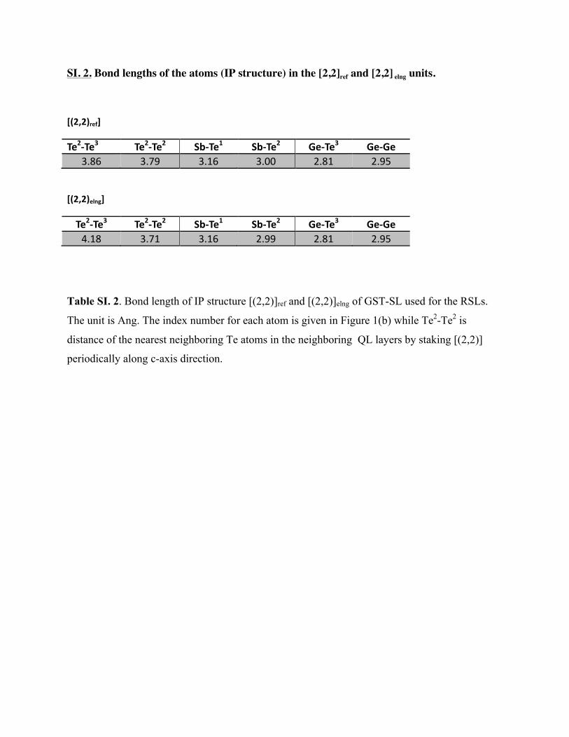
SI. 2. Bond lengths of the atoms (IP structure) in the [2,2]ref and [2,2] elng units.
[(2,2)ref]
Te2-Te3 Te2-Te2 Sb-Te1 Sb-Te2 Ge-Te3 Ge-Ge3.86 3.79 3.16 3.00 2.81 2.95
[(2,2)elng]
Te2-Te3 Te2-Te2 Sb-Te1 Sb-Te2 Ge-Te3 Ge-Ge4.18 3.71 3.16 2.99 2.81 2.95
Table SI. 2. Bond length of IP structure [(2,2)]ref and [(2,2)]elng of GST-SL used for the RSLs.
The unit is Ang. The index number for each atom is given in Figure 1(b) while Te2-Te2 is
distance of the nearest neighboring Te atoms in the neighboring QL layers by staking [(2,2)]
periodically along c-axis direction.
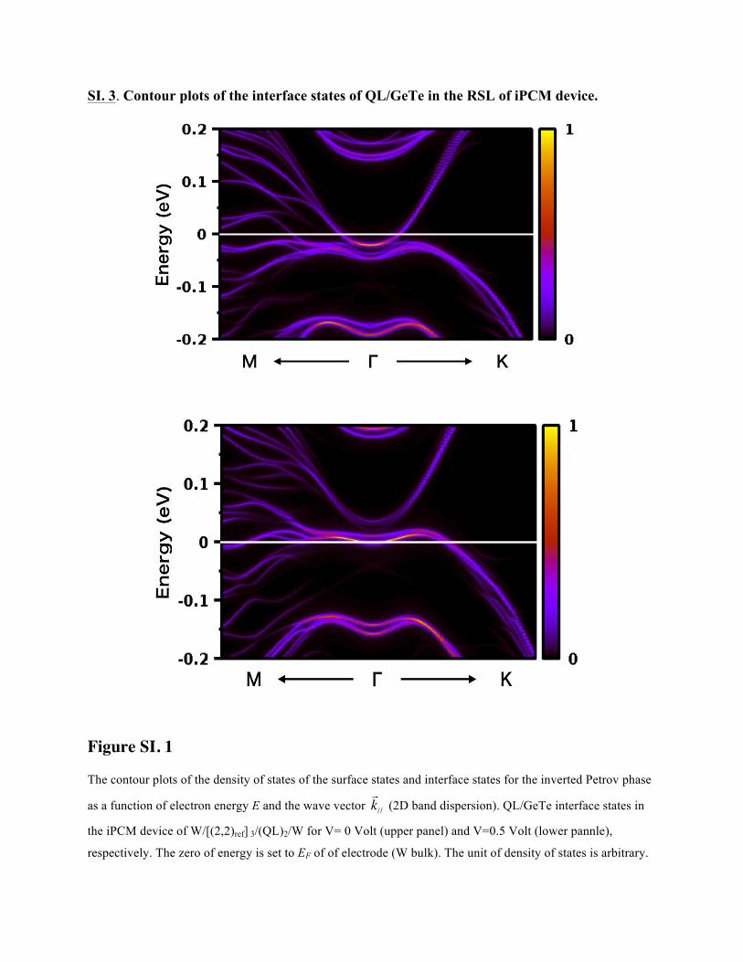
SI. 3. Contour plots of the interface states of QL/GeTe in the RSL of iPCM device.
Figure SI. 1
The contour plots of the density of states of the surface states and interface states for the inverted Petrov phase
as a function of electron energy E and the wave vector !k// (2D band dispersion). QL/GeTe interface states in
the iPCM device of W/[(2,2)ref] 3/(QL)2/W for V= 0 Volt (upper panel) and V=0.5 Volt (lower pannle),
respectively. The zero of energy is set to EF of of electrode (W bulk). The unit of density of states is arbitrary.

SI. 4. Contour plots of the transmission coefficient
In the Figure SI.2, we show the calculated transmission coefficients as a function of the energy E
and the wave vector !k// for the device model W/[(2,2)ref]3(QL)2/W. The transmission coefficient
resolved by !k// can be calculated as follows:
T (E,!k// )= Tr[ΓR(E,
!k// )G(E,
!k// )ΓR(E,
!k// )G†(E,
!k// )]
where G is the (retarded) Green’s function by the Bloch Hamiltonian H (!k// ) and ΓL/R is
i(ΣL/R − ΣL/R† ) where ΣL/R is the self-energy of the left/right leads. The upper, middle and the
lower panels are the contour plots of log10T (E,!k// ) for IP, P(v), and FGT(vl) structures,
respectively. For each structure, the plots are the result by V=0 Volt (left panel) and 0.5 Volt
(right panel), respectively.

Figure SI. 2
The upper, middle and the lower panels are the contour plots of log10T (E,!k// ) for IP, P(v), and
FGT(vl) structures, respectively. For each structure, the plots are the result when the applied bias
V is 0 Volt (left panel) and 0.5 Volt (right panel), respectively.