Embed Size (px)
Citation preview
Independent Biasing (7/14/00) Page 1
ECE 4430 - Analog Integrated Circuits and Systems P.E. Allen, 2000
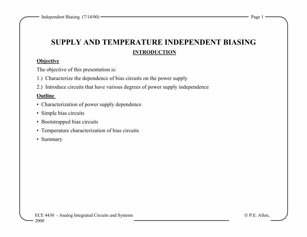
SUPPLY AND TEMPERATURE INDEPENDENT BIASING INTRODUCTION
Objective The objective of this presentation is: 1.) Characterize the dependence of bias circuits on the power supply 2.) Introduce circuits that have various degrees of power supply independence Outline • Characterization of power supply dependence • Simple bias circuits • Bootstrapped bias circuits • Temperature characterization of bias circuits • Summary

Independent Biasing (7/14/00) Page 2
ECE 4430 - Analog Integrated Circuits and Systems P.E. Allen, 2000
CHARACTERIZATION OF POWER SUPPLY DEPENDENCE
Characteristics of a Voltage or Current Reference What is a Voltage or Current Reference? A voltage or current reference is an independent voltage or current source that has a high degree of precision and stability. Requirements of a Reference Circuit: • Should be independent of power supply • Should be independent of temperature • Should be independent of processing variations • Should be independent of noise and other interference
Reference
Noise
Temperature
Power Supply
NominalValue
Fig. 4.5-1

Independent Biasing (7/14/00) Page 3
ECE 4430 - Analog Integrated Circuits and Systems P.E. Allen, 2000
Power Supply Independence How do you characterize power supply independence? Use the concept of sensitivity (we will use voltage although IREF can be substituted for VREF in the following):
SVREF
VDD =
VREF/VREFVDD/VDD
= VDDVREF
VREF
VDD
Application of sensitivity to determining power supply dependence:
VREF
VREF =
SVREF
VDD
VDDVDD
Thus, the fractional change in the reference voltage is equal to the sensitivity times the fractional change in the power supply voltage. For example, if the sensitivity is 1, then a 10% change in VDD will cause a 10% change in VREF.
Ideally, we want SVREF
VDD to be zero for power supply independence.
Independent Biasing (7/14/00) Page 4
ECE 4430 - Analog Integrated Circuits and Systems P.E. Allen, 2000
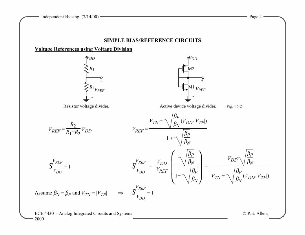
SIMPLE BIAS/REFERENCE CIRCUITS Voltage References using Voltage Division
M2
M1
VDDVDD
R1
R2
+
-
VREF
+
-
VREF
Resistor voltage divider. Active device voltage divider. Fig. 4.5-2
VREF = R2
R1+R2 VDD VREF =
VTN + βPβN
(VDD-|VTP|)
1 + βPβN
SVREF
VDD = 1 S
VREF
VDD =
VDDVREF
βP
βN
1+ βPβN
= VDD
βPβN
VTN + βPβN
(VDD-|VTP|)
Assume βN = βP and VTN = |VTP| ⇒ SVREF
VDD = 1
Independent Biasing (7/14/00) Page 5
ECE 4430 - Analog Integrated Circuits and Systems P.E. Allen, 2000
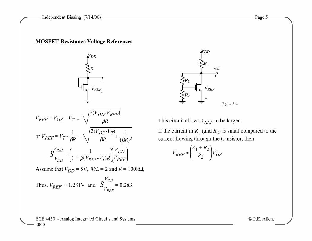
MOSFET-Resistance Voltage References
vout
VDD
+
-
R
VREF
VDD
+
-
R
VREF
R1
R2
Fig. 4.5-4
VREF = VGS = VT + 2(VDD-VREF)
βR
or VREF = VT - 1
βR + 2(VDD-VT)
βR + 1
(βR)2
SVREF
VDD =
1
1 + β(VREF-VT)R
VDD
VREF
Assume that VDD = 5V, W/L = 2 and R = 100kΩ,
Thus, VREF ≈ 1.281V and SVDD
VREF = 0.283
This circuit allows VREF to be larger.
If the current in R1 (and R2) is small compared to the current flowing through the transistor, then
VREF ≈
R1 + R2
R2 VGS
Independent Biasing (7/14/00) Page 6
ECE 4430 - Analog Integrated Circuits and Systems P.E. Allen, 2000
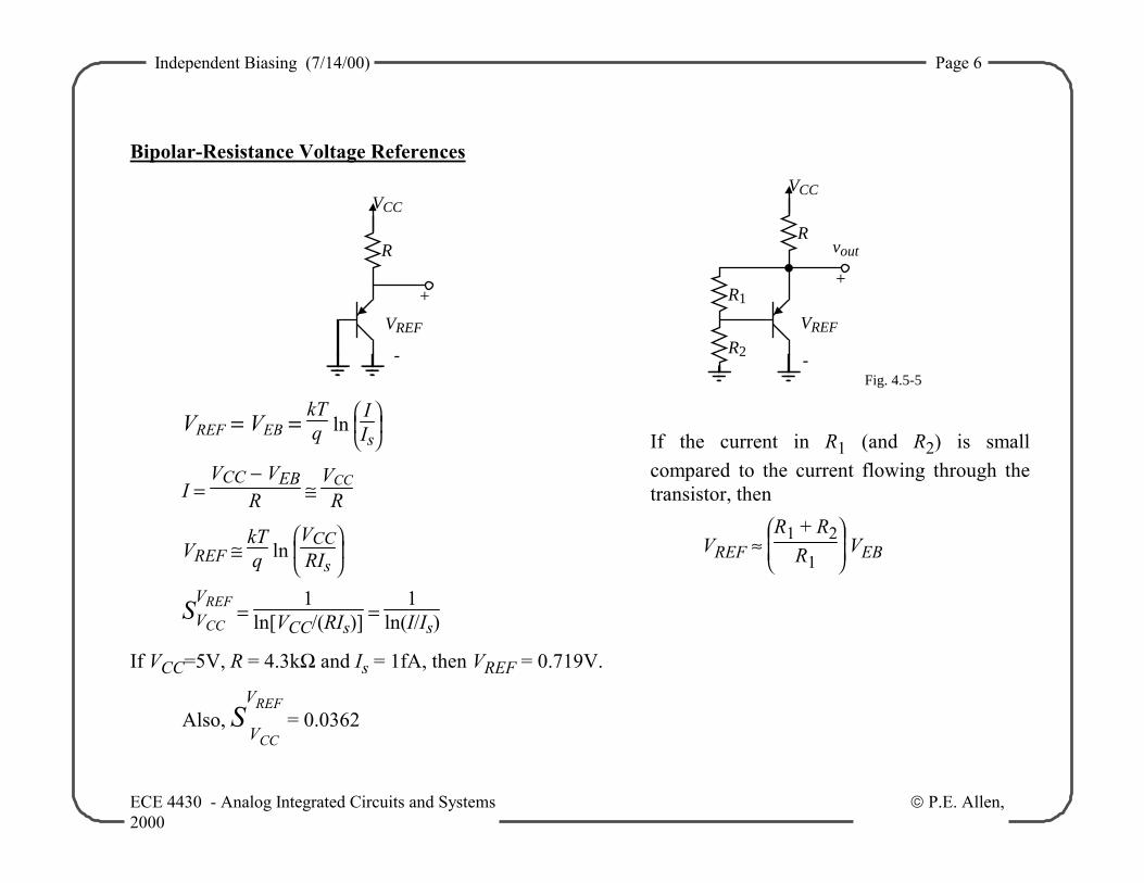
Bipolar-Resistance Voltage References
vout
VCC
+
-
R
VREF
VCC
+
-
R
VREF
R1
R2
Fig. 4.5-5
VREF = VEB = kTq ln
I
Is
I = VCC − VEB
R ≅ VCCR
VREF ≅ kTq ln
VCC
RIs
SVREFVCC
= 1
ln[VCC/(RIs)] =
1ln(I/Is)
If VCC=5V, R = 4.3kΩ and Is = 1fA, then VREF = 0.719V.
Also, SVREF
VCC = 0.0362
If the current in R1 (and R2) is small compared to the current flowing through the transistor, then
VREF ≈
R1 + R2
R1 VEB
Independent Biasing (7/14/00) Page 7
ECE 4430 - Analog Integrated Circuits and Systems P.E. Allen, 2000

Independent Biasing (7/14/00) Page 8
ECE 4430 - Analog Integrated Circuits and Systems P.E. Allen, 2000
Example 1 - Design of a Higher-Voltage Bipolar Voltage Reference Use the circuit on the previous slide to design a voltage reference having VREF = 2.5V when VCC = 5V. Assume Is = 1fA and βF = 100. Evaluate the sensitivity of VREF with respect to VCC.
Solution
Choose I (the current flowing through R) to be 100µA. Therefore R = VCC-VREF
100µA = 2.5V
100µA = 25kΩ.
Choose I1(the current flowing through R1) to be 50µA. Therefore the current flowing in the emitter is
50µA. The value of VEB = Vt ln
50µA
1fA = 0.638V.
∴ R1 = 0.638V50µA = 12.76kΩ
With 50µA in the emitter, the base current is approximately 5µA. Therefore, the current through R2 is 55µA.
Since VREF = IR2R2 + 0.638V = 2.5V, we get R2 =
2.5V-0.638V
55µA = 33.85kΩ.
The sensitivity of VREF with respect to VCC is
SVREF’
VCC =
R1+ R2
R1S
VREF
VCC =
12.76kΩ+33.85kΩ
12.76kΩ
1
ln(IQ/Is) = 3.652(0.0406) = 0.148
Independent Biasing (7/14/00) Page 9
ECE 4430 - Analog Integrated Circuits and Systems P.E. Allen, 2000
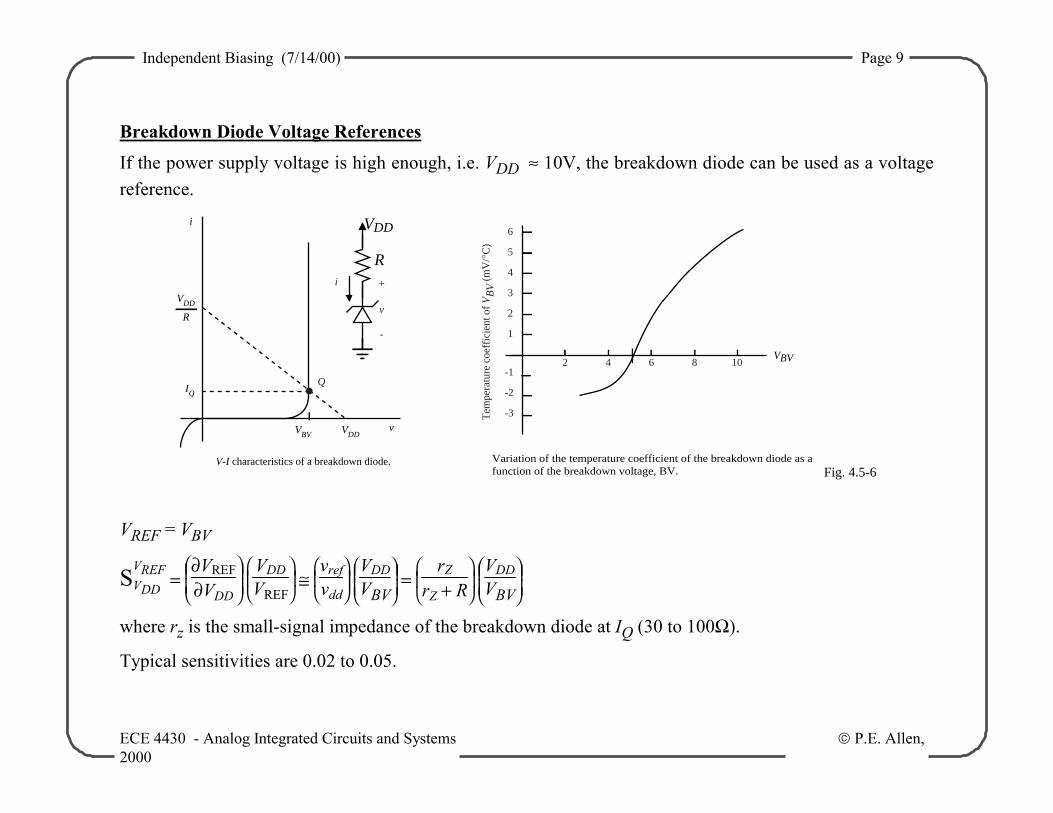
Breakdown Diode Voltage References
If the power supply voltage is high enough, i.e. VDD ≈ 10V, the breakdown diode can be used as a voltage reference.
V-I characteristics of a breakdown diode.
i
vVBV VDD
VDD
R
IQ
i +
-
v
Q
Variation of the temperature coefficient of the breakdown diode as afunction of the breakdown voltage, BV.
2 4 6 8 10
1
2
3
4
5
6
-3
-2
-1
VBV
Tem
pera
ture
coe
ffic
ient
of
VB
V (
mV
/°C
)Fig. 4.5-6
VDD
R
VREF = VBV
SVREFVDD =
∂VREF
∂VDD
VDD
VREF ≅
vref
vdd
VDD
VBV =
rZ
rZ + R
VDD
VBV
where rz is the small-signal impedance of the breakdown diode at IQ (30 to 100Ω).
Typical sensitivities are 0.02 to 0.05.

Independent Biasing (7/14/00) Page 10
ECE 4430 - Analog Integrated Circuits and Systems P.E. Allen, 2000
Note that the temperature dependence could be zero if VB was a variable.
Independent Biasing (7/14/00) Page 11
ECE 4430 - Analog Integrated Circuits and Systems P.E. Allen, 2000
BOOTSTRAPPED BIAS/REFERENCE CIRCUITS Bootstrapped Current Source So far, none of the previous references have shown very good independence from power supply. Let us now examine a technique which does achieve the desired independence. Circuit:
i
v
IQ
VQ
RI2 =
WL
I1 = (VGS1 - VT)2
M2
+
-
M1
I5
M8
VGS1
M3M4
R
I6
M5
M6
I1 I2
Startup
VDD
VGS1M7
IR02
Desiredoperatingpoint
Undesiredoperatingpoint
0V
K'N2RB
Principle:
If M3 = M4, then I1 ≈ I2. However, the M1-R loop gives VGS1 = VT1 + 2I1
KN’(W1/L1)
Solving these two equations gives I2 = VGS1
R = VT1R +
1
R 2I1
KN’(W1/L1)
The output current, Iout = I1 = I2 can be solved as Iout = VT1R +
1β1R2 +
1R
2VT1β1R +
1(β1R)2

Independent Biasing (7/14/00) Page 12
ECE 4430 - Analog Integrated Circuits and Systems P.E. Allen, 2000
which is not dependent upon the power supply.
Independent Biasing (7/14/00) Page 13
ECE 4430 - Analog Integrated Circuits and Systems P.E. Allen, 2000
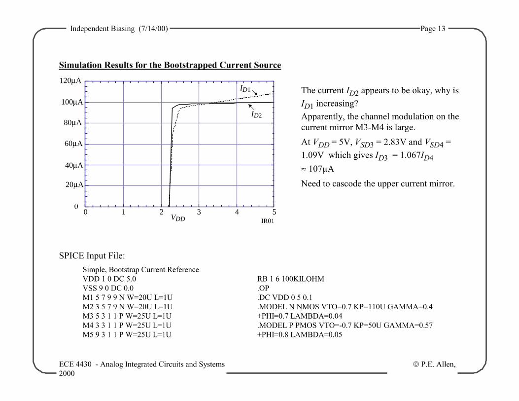
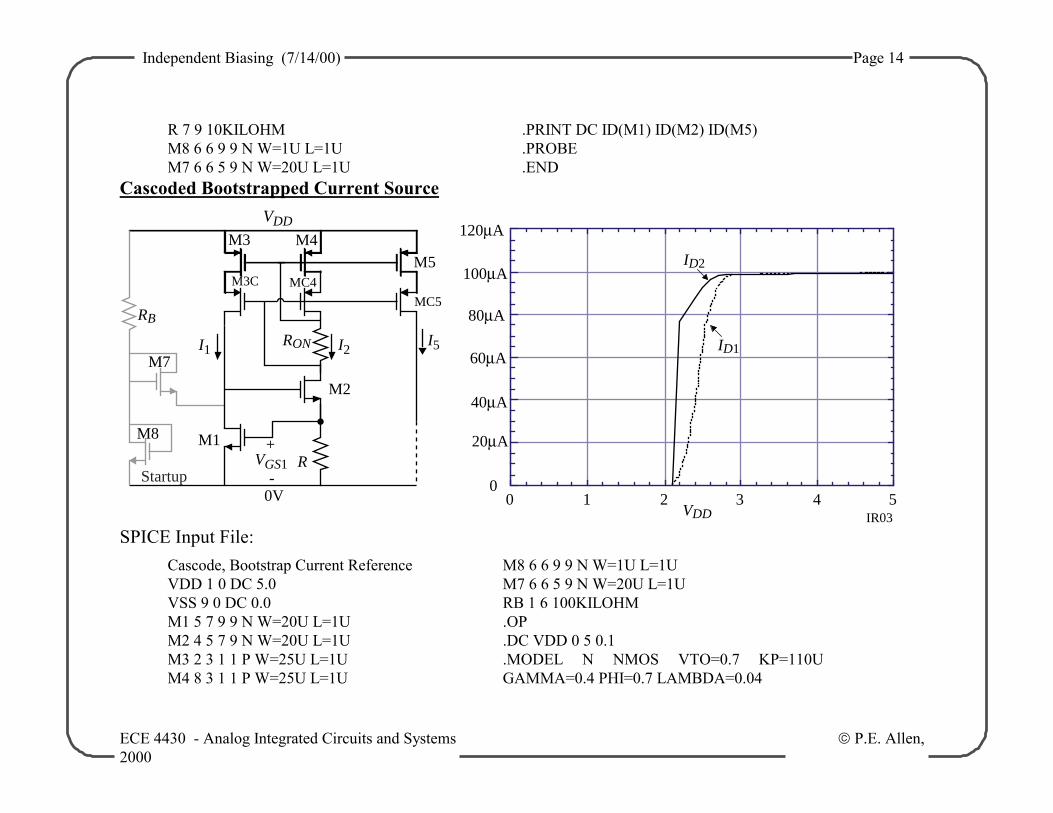
Simulation Results for the Bootstrapped Current Source The current ID2 appears to be okay, why is ID1 increasing? Apparently, the channel modulation on the current mirror M3-M4 is large. At VDD = 5V, VSD3 = 2.83V and VSD4 = 1.09V which gives ID3 = 1.067ID4 ≈ 107µA Need to cascode the upper current mirror.
SPICE Input File: Simple, Bootstrap Current Reference
VDD 1 0 DC 5.0 VSS 9 0 DC 0.0 M1 5 7 9 9 N W=20U L=1U M2 3 5 7 9 N W=20U L=1U M3 5 3 1 1 P W=25U L=1U M4 3 3 1 1 P W=25U L=1U M5 9 3 1 1 P W=25U L=1U
RB 1 6 100KILOHM .OP .DC VDD 0 5 0.1 .MODEL N NMOS VTO=0.7 KP=110U GAMMA=0.4 +PHI=0.7 LAMBDA=0.04 .MODEL P PMOS VTO=-0.7 KP=50U GAMMA=0.57 +PHI=0.8 LAMBDA=0.05
0 1 2 3 4 5VDD
120µA
100µA
80µA
60µA
40µA
20µA
0
ID1
ID2
IR01
Independent Biasing (7/14/00) Page 14
ECE 4430 - Analog Integrated Circuits and Systems P.E. Allen, 2000
R 7 9 10KILOHM M8 6 6 9 9 N W=1U L=1U M7 6 6 5 9 N W=20U L=1U
.PRINT DC ID(M1) ID(M2) ID(M5)
.PROBE
.END Cascoded Bootstrapped Current Source
0 1 2 3 4 5VDD
120µA
100µA
80µA
60µA
40µA
20µA
0
ID1
ID2
IR03
M2
+
-
M1
I5
M8
VGS1
M3 M4
R
M5
I1 I2
Startup
VDD
M7
0V
RB
M3C MC4
MC5
RON
SPICE Input File: Cascode, Bootstrap Current Reference
VDD 1 0 DC 5.0 VSS 9 0 DC 0.0 M1 5 7 9 9 N W=20U L=1U M2 4 5 7 9 N W=20U L=1U M3 2 3 1 1 P W=25U L=1U M4 8 3 1 1 P W=25U L=1U
M8 6 6 9 9 N W=1U L=1U M7 6 6 5 9 N W=20U L=1U RB 1 6 100KILOHM .OP .DC VDD 0 5 0.1 .MODEL N NMOS VTO=0.7 KP=110U GAMMA=0.4 PHI=0.7 LAMBDA=0.04
Independent Biasing (7/14/00) Page 15
ECE 4430 - Analog Integrated Circuits and Systems P.E. Allen, 2000
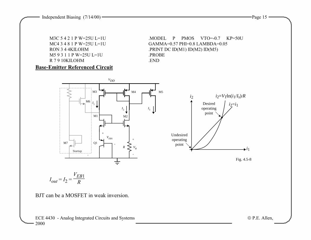
M3C 5 4 2 1 P W=25U L=1U MC4 3 4 8 1 P W=25U L=1U RON 3 4 4KILOHM M5 9 3 1 1 P W=25U L=1U R 7 9 10KILOHM
.MODEL P PMOS VTO=-0.7 KP=50U GAMMA=0.57 PHI=0.8 LAMBDA=0.05 .PRINT DC ID(M1) ID(M2) ID(M5) .PROBE .END
Base-Emitter Referenced Circuit
M2
+
-
+
-
M1
I5
M7
-
VEB1
VR
M3 M4
R
M5
I1
I2
Startup
Q1
VDD
Fig. 4.5-8
i2
i1
Desiredoperating
point
Undesiredoperating
point
i2=VTln(i1/Is)/R
i2=i1M6
Iout = I2 = VEB1
R
BJT can be a MOSFET in weak inversion.
Independent Biasing (7/14/00) Page 16
ECE 4430 - Analog Integrated Circuits and Systems P.E. Allen, 2000
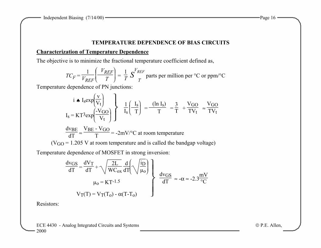
TEMPERATURE DEPENDENCE OF BIAS CIRCUITS Characterization of Temperature Dependence The objective is to minimize the fractional temperature coefficient defined as,
TCF = 1
VREF
VREF
T = 1T S
VREF
T parts per million per °C or ppm/°C
Temperature dependence of PN junctions:
i ♠ Isexp
v
Vt
Is = KT3exp
-VGO
Vt
1Is
Is
T = (ln Is)
T = 3T +
VGOTVt
≈ VGOTVt
dvBEdT ≈
VBE - VGOT = -2mV/°C at room temperature
(VGO = 1.205 V at room temperature and is called the bandgap voltage)
Temperature dependence of MOSFET in strong inversion:
dvGSdT =
dVTdT +
2LWCox
d
dT
iD
µo
µo = KT-1.5
VT(T) = VT(To) - α(T-To)
dvGSdT ≈ -α ≈ -2.3
mV°C
Resistors:

Independent Biasing (7/14/00) Page 17
ECE 4430 - Analog Integrated Circuits and Systems P.E. Allen, 2000
1R
dRdT ppm/°C
Independent Biasing (7/14/00) Page 18
ECE 4430 - Analog Integrated Circuits and Systems P.E. Allen, 2000
Bipolar-Resistance Voltage References From previous work we know that,
VREF = kTq ln
VDD - VREF
RIs
However, not only is VREF a function of T, but R and Is are also functions of T.
∴ dVREF
dT = kq ln
VDD-VREF
RIs +
kTq
RIs
VDD-VREF
-1
RIs dVREF
dT -
VDD-VREF
RIs
dR
RdT + dIs
IsdT
= VREF
T - Vt
VDD-VREF dVREF
dT - Vt
dR
RdT + dIs
IsdT = VREF-VGO
T - Vt
VDD-VREF dVREF
dT - 3VtT -
VtR
dRdT
∴ dVREF
dT =
VREF-VGOT - Vt
dRRdT -
3VtT
1 + Vt
VDD-VREF
≈ VREF-VGO
T - Vt dR
RdT - 3VtT
TCF = 1
VREF dVREF
dT = VREF-VGO
VREF·T - Vt
VREF
dRRdT -
3VtVREF·T
If VREF = 0.6V, Vt = 0.026V, and the resistor is polysilicon, then at room temperature the TCF is
TCF = 0.6-1.2050.6·300 -
0.026·0.00150.6 -
3·0.0260.6·300 = -3361x10-6-65x10-6-433x10-6 =-3859ppm/°C
VDD
+
-
R
VREF
Fig. 4.5-9
Independent Biasing (7/14/00) Page 19
ECE 4430 - Analog Integrated Circuits and Systems P.E. Allen, 2000
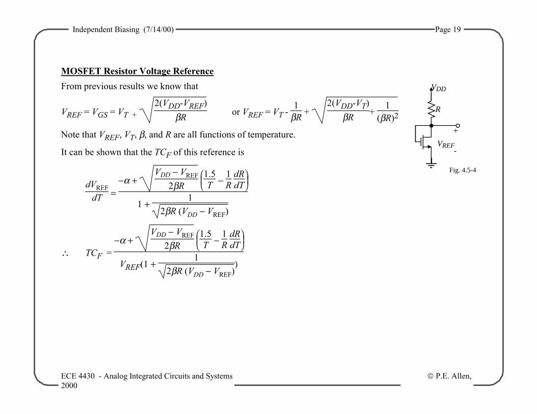
MOSFET Resistor Voltage Reference From previous results we know that
VREF = VGS = VT + 2(VDD-VREF)
βR or VREF = VT - 1
βR + 2(VDD-VT)
βR + 1
(βR)2
Note that VREF, VT, β, and R are all functions of temperature.
It can be shown that the TCF of this reference is
dVREF
dT = −α +
VDD − VREF
2βR
1.5
T − 1R
dRdT
1 + 1
2βR (VDD − VREF)
∴ TCF = −α +
VDD − VREF
2βR
1.5
T − 1R
dRdT
VREF(1 + 1
2βR (VDD − VREF))
VDD
+
-
R
VREF
Fig. 4.5-4

Independent Biasing (7/14/00) Page 20
ECE 4430 - Analog Integrated Circuits and Systems P.E. Allen, 2000
Example 1 - Calculation of MOSFET-Resistor Voltage Reference TCF Calculate the temperature coefficient of the MOSFET-Resistor voltage reference where W/L=2, VDD=5V, R=100kΩ using the parameters of Table 3.1-2. The resistor, R, is polysilicon and has a tempco of 1500 ppm/°C. Solution
First, calculate VREF . Note that βR = 220x10-6 ∞ 105 = 22V-1 and dR
RdT = 1500ppm/°C
∴ VREF = 0.7 − 122 +
2(5 − 0.7)22 +
1
222
= 1.281V
Now, dVREF
dT = −2.3∞10-3 +
5 − 1.2812(22)
1.5
300 − 1500 ∞ 10-6
1 + 1
2(22) (5 - 1.281)
= -1.189x10⁻³V/°C
The fractional temperature coefficient is given by
TCF = −1.189 ∞ 10-3
1
1.281 = −928 ppm/ C

Independent Biasing (7/14/00) Page 21
ECE 4430 - Analog Integrated Circuits and Systems P.E. Allen, 2000
Bootstrapped Current Source/Sink Gate-source referenced source:
The output current was given as, Iout = VT1R +
1β1R2 +
1R
2VT1β1R +
1(β1R)2
Although we could grind out the derivative of Iout with respect to T, the temperature performance of this circuit is not that good to spend the time to do so. Therefore, let us assume that VGS1 ≈ VT1 which gives
Iout ≈ VT1R ⇒
dIoutdT =
1R
dVT1dT -
1R2
dRdT
In the resistor is polysilicon, then
TCF = 1
Iout dIoutdT =
1VT1
dVT1dT -
1R
dRdT =
-αVT1
- 1R
dRdT =
-2.3x10⁻³
0.7 - 1.5x10-3 = -4786ppm/°C
Base-emitter referenced source:
The output current was given as, Iout = I2 = VBE1
R
The TCF = 1
VBE1 dVBE1
dT - 1R
dRdT
If VBE1 = 0.6V and the resistor is poly, then the TCF = 1
0.6 (-2x10⁻³) - 1.5x10-3 = -4833ppm/°C.

Independent Biasing (7/14/00) Page 22
ECE 4430 - Analog Integrated Circuits and Systems P.E. Allen, 2000
Zero Temperature Coefficient (ZTC) Point for MOSFETs For a given value of gate-source voltage, the drain current of the MOSFET will be independent of temperature. Consider the following circuit:
Assume that the transistor is saturated and that:
µ = µo
T
To
-1.5 and VT(T) = VT(To) + α(T-To)
where α = -0.0023V/°C and To = 27°C
∴ ID(T) = µoCoxW
2L
T
To
-1.5[VGS - VT0 - α(T-To)]2
dIDdT =
-1.5µoCox2To
T
To
-2.5[VGS - VT0 - α(T-To)]2 + αµoCox
T
To
-1.5[VGS - VT0 - α(T-To)] = 0
∴ VGS - VT0 - α(T-To) = -4Tα
3 ⇒ VGS(ZTC) = VT0 - αTo - αΤ3
Let K’ = 10µA/V2, W/L = 5 and VT0 = 0.71V.
At T = 27°C (300°K), VGS(ZTC) = 0.71 - (-0.0023)(300°K) -(0.333)(-0.0023)(300°K) = 1.63V
At T = 27°C (300°K), ID = (10µA/V2)(5/2)(1.63-0.71)2 = 21.2µA
At T = 200°C (473°K), VGS(ZTC) = 0.71 - (-0.0023)(300°K) -(0.333)(-0.0023)(473°K) = 1.76V
ID
VGS
Fig. 4.5-12
Independent Biasing (7/14/00) Page 23
ECE 4430 - Analog Integrated Circuits and Systems P.E. Allen, 2000
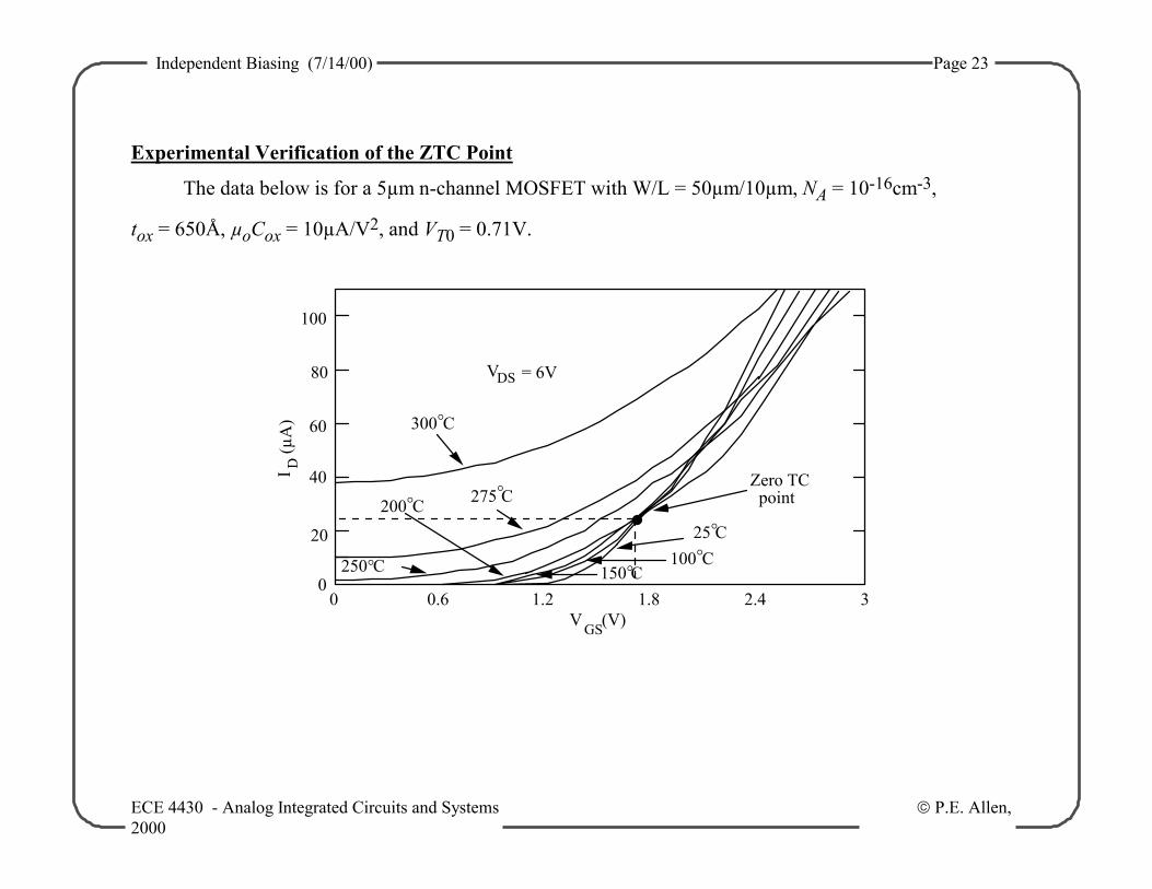
Experimental Verification of the ZTC Point
The data below is for a 5µm n-channel MOSFET with W/L = 50µm/10µm, NA = 10-16cm-3,
tox = 650Å, µoCox = 10µA/V2, and VT0 = 0.71V.
0
20
40
60
80
100
0 0.6 1.2 1.8 2.4 3
300°C
275°C
250°C
200°C
150°C100°C
25°C
Zero TC point
V GS(V)
I D(µ
A)
VDS = 6V
Independent Biasing (7/14/00) Page 24
ECE 4430 - Analog Integrated Circuits and Systems P.E. Allen, 2000
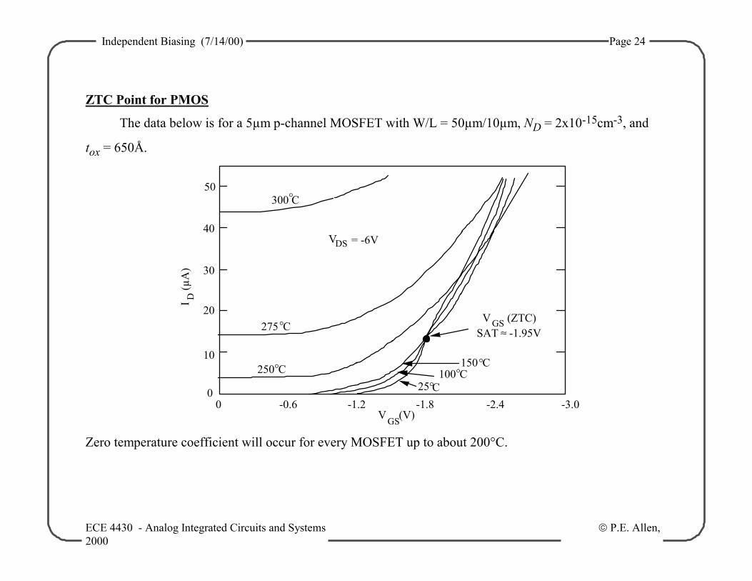
ZTC Point for PMOS
The data below is for a 5µm p-channel MOSFET with W/L = 50µm/10µm, ND = 2x10-15cm-3, and
tox = 650Å.
0
10
20
30
40
50
0 -0.6 -1.2 -1.8 -2.4 -3.0
300°C
275°C
250°C 150°C100°C
25°C
V GS (ZTC)SAT ≈ -1.95V
VGS(V)
I D(µ
A)
VDS = -6V
Zero temperature coefficient will occur for every MOSFET up to about 200°C.
Independent Biasing (7/14/00) Page 25
ECE 4430 - Analog Integrated Circuits and Systems P.E. Allen, 2000
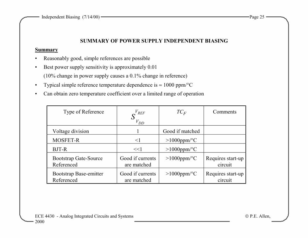
SUMMARY OF POWER SUPPLY INDEPENDENT BIASING Summary • Reasonably good, simple references are possible • Best power supply sensitivity is approximately 0.01 (10% change in power supply causes a 0.1% change in reference)
• Typical simple reference temperature dependence is ≈ 1000 ppm/°C • Can obtain zero temperature coefficient over a limited range of operation
Type of Reference S
VREF
VDD
TCF Comments
Voltage division 1 Good if matched
MOSFET-R <1 >1000ppm/°C
BJT-R <<1 >1000ppm/°C
Bootstrap Gate-Source Referenced
Good if currents are matched
>1000ppm/°C Requires start-up circuit
Bootstrap Base-emitter Referenced
Good if currents are matched
>1000ppm/°C Requires start-up circuit

Independent Biasing (7/14/00) Page 26
ECE 4430 - Analog Integrated Circuits and Systems P.E. Allen, 2000
Independent Biasing (7/14/00) Page 27
ECE 4430 - Analog Integrated Circuits and Systems P.E. Allen, 2000