Embed Size (px)
Citation preview
Instructions for use
Title Surface-related operation instabilities of GaN HEMTs and their control using Al2O3-based MOS structures
Author(s) 西口, 賢弥
Citation 北海道大学. 博士(工学) 甲第13083号
Issue Date 2018-03-22
DOI 10.14943/doctoral.k13083
Doc URL http://hdl.handle.net/2115/70528
Type theses (doctoral)
File Information Kenya_Nishiguchi.pdf
Hokkaido University Collection of Scholarly and Academic Papers : HUSCAP
博士論文
Surface-related operation instabilities of GaN HEMTs and
their control using Al2O3-based MOS structures
GaN HEMTにおける表面起因の動作不安定性と Al2O3
MOS構造を用いた制御
Kenya Nishiguchi
西口 賢弥
Graduate School of Information Science and Technology
Hokkaido University
北海道大学大学院 情報科学研究科
February, 2018

3
Acknowledgements
First of all, I would like to thank my supervisor, Prof. Tamotsu Hashizume. He
guided and adviced me sincerely throughout my bachelor, master, and doctoral
courses. I wanted to give up to graduate doctoral course many times. However, I
could get finally great results and knowledge about my research theme. These six
years under his direction are irreplaceable for me. He is the best professor.
I am thankful to Prof. Takashi Fukui, Prof. Eiichi Sano, Prof. Junichi Motohisa,
Prof. Shinjiro Hara, and Prof. Katsuhiro Tomioka for helping me study in RCIQE.
Furthermore, I wish to thank to thank to Prof. Masamichi Akazawa, Prof. Taketomo
Sato, and Prof. Seiya Kasai, the supervisors of our seminar group, for advising and
discussing me during my study.
I wish to thank to my ex-colleagues, Dr. Kota Ohi and Dr. Yujin Hori. They
advised me that the importance of doctoral course. In addition, I am thankful to
Mr. Yutaka Senzaki. I worked hard with him. Furthermore, I am thankful to Dr.
Joel T. Asubar and Dr. Zenji Yatabe. They helped me many times when I was
depressed.
I wish to thank the current members of “Hashizume-group”, Dr. Maciek Matys,
Mr. Shiro Ozaki, Mr. Shota Kaneki, Mr. Shota Toiya, Yuji Ando, Tatsuya Oyobiki,
and Syota Sasaki. They helped my research.
I would like to thank to Dr. Marchin Miczek and Dr. Junji Kotani. Each of them
developed a very wonderful simulator by using C language. Kotani’s simulator
taught me how to calculate potential distribution and TFE curret. And, Marchin’s
simulator taught me how to calculate C-V characteristics with interface states. I
developed C-V calculation simulator based on both programs. This is the most
important property of my university school life.
I wish to thank to Prof. Testu Kachi of Nagoya Univ., Dr. Naoki Hara of Fujitsu

4 Acknowledgements
Lab., Dr. Masataka Higashiwaki of National Institute of Information and Communi-
cations Technology (NICT), and Dr. Yasuo Koide of National Institute for Materials
Science (NIMS). They discussed and advised me about my research theme.
I really appreciate to Dr. Hajime Fujikura, Dr. Masafumi Horikiri, and members
of SCIOCS, Tetsuo Narita and members of Toyota Central Research and Develop-
ment Laboratories, Inc. They provided very high quality epilayers for our group.
I really appreciate Dr. Dagmar Gregusova for sharing a lot of wonderful time
with me throughout the collaboration reseach and many conferences. Furthemore,
I would like to express many thanks to Prof. Jan Kuzmik, Dr. Milan Tapajna, and
members of Slovak Academy of Sciences, for always discussing and advising me very
kindly.
I would like to thank to Prof. Bouguslawa Adamowicz, and members of Silesian
University of Technology, for giving me the opportunities to have the collaboration
works with you.
I really appreciate Kentaro Sasaki and Ryutaro Kodaira. They are best colleague.
最後になりましたが、私の学位取得を最後まで応援してくださった両親、妹、
そして妻に深く感謝申し上げます。
February, 2018 at RCIQE
Kenya Nishiguchi
5
Contents
Chapter 1 Introduction 7
1.1 Background . . . . . . . . . . . . . . . . . . . . . . . . . . . . . 7
1.2 Benefits of Using Gallium Nitride (GaN) . . . . . . . . . . . . . 9
1.3 GaN-based High Electron Mobility Transistors (HEMTs) . . . . 12
1.4 Merits of Metal-Insulator-Semiconductor (MIS) Structure . . . 13
1.5 Several Issues of GaN-based HEMTs . . . . . . . . . . . . . . . 15
1.6 Purpose of this Work . . . . . . . . . . . . . . . . . . . . . . . . 18
1.7 Outline . . . . . . . . . . . . . . . . . . . . . . . . . . . . . . . 18
References 21
Chapter 2 Physical properties of GaN 25
2.1 Basic Properties of III-N Semiconductor Materials . . . . . . . 25
2.2 The state of the art of Growth Method and Quality of GaN
Crystal . . . . . . . . . . . . . . . . . . . . . . . . . . . . . . . 26
2.3 AlGaN/GaN heterojunction . . . . . . . . . . . . . . . . . . . . 27
References 35
Chapter 3 Electronic States at Interface or Surface of Semicon-
ductor 37
3.1 Introduction . . . . . . . . . . . . . . . . . . . . . . . . . . . . 37
3.2 Fermi level Pinning and it’s Origin . . . . . . . . . . . . . . . . 37
3.3 Charge neutrality level . . . . . . . . . . . . . . . . . . . . . . . 38
3.4 Metal-induced gap state model (MIGS) . . . . . . . . . . . . . 39
3.5 Disorder-Induced Gap State Model (DIGS) . . . . . . . . . . . 39
3.6 Unified defect model (UDM) . . . . . . . . . . . . . . . . . . . 41
6 Contents
3.7 Influence of interface states at the insulator/GaN interface on
the capacitance-voltage behavior of insulator/GaN MOS struc-
tures . . . . . . . . . . . . . . . . . . . . . . . . . . . . . . . . . 41
3.8 Theoretical C-V curves of the Al2O3/GaN structure . . . . . . 44
3.9 Special Case of Interface States distributed both in energy and
space . . . . . . . . . . . . . . . . . . . . . . . . . . . . . . . . 48
References 55
Chapter 4 Evaluation of surface charging at AlGaN surface using
a dual-gate structure 59
4.1 Background . . . . . . . . . . . . . . . . . . . . . . . . . . . . . 59
4.2 Device structure and fabrication process . . . . . . . . . . . . . 60
4.3 Results and discussions . . . . . . . . . . . . . . . . . . . . . . 61
4.4 Conclusion . . . . . . . . . . . . . . . . . . . . . . . . . . . . . 68
References 69
Chapter 5 Current linearity and operation stability in GaN MIS
HEMTs 71
5.1 Background . . . . . . . . . . . . . . . . . . . . . . . . . . . . . 71
5.2 Device Fabrication Processes . . . . . . . . . . . . . . . . . . . 72
5.3 Extremely Decreased Electronic States at Al2O3/n-GaN Inter-
face by Reverse-Bias Annealing . . . . . . . . . . . . . . . . . . 73
5.4 Results and Discussion . . . . . . . . . . . . . . . . . . . . . . . 76
5.5 Conclusions . . . . . . . . . . . . . . . . . . . . . . . . . . . . . 87
References 89
Chapter 6 Conclusion 93
7
Chapter 1
Introduction
1.1 Background
In recent years, the technological innovation in the field of information technology
has been remarkable. The spread of information devices such as personal computers,
the expansion of the role of the Internet and the spread of satellite broadcasting are
progressing rapidly. However, there are several problems in the field of information
technology.
1.1.1 Volume of mobile communication traffic
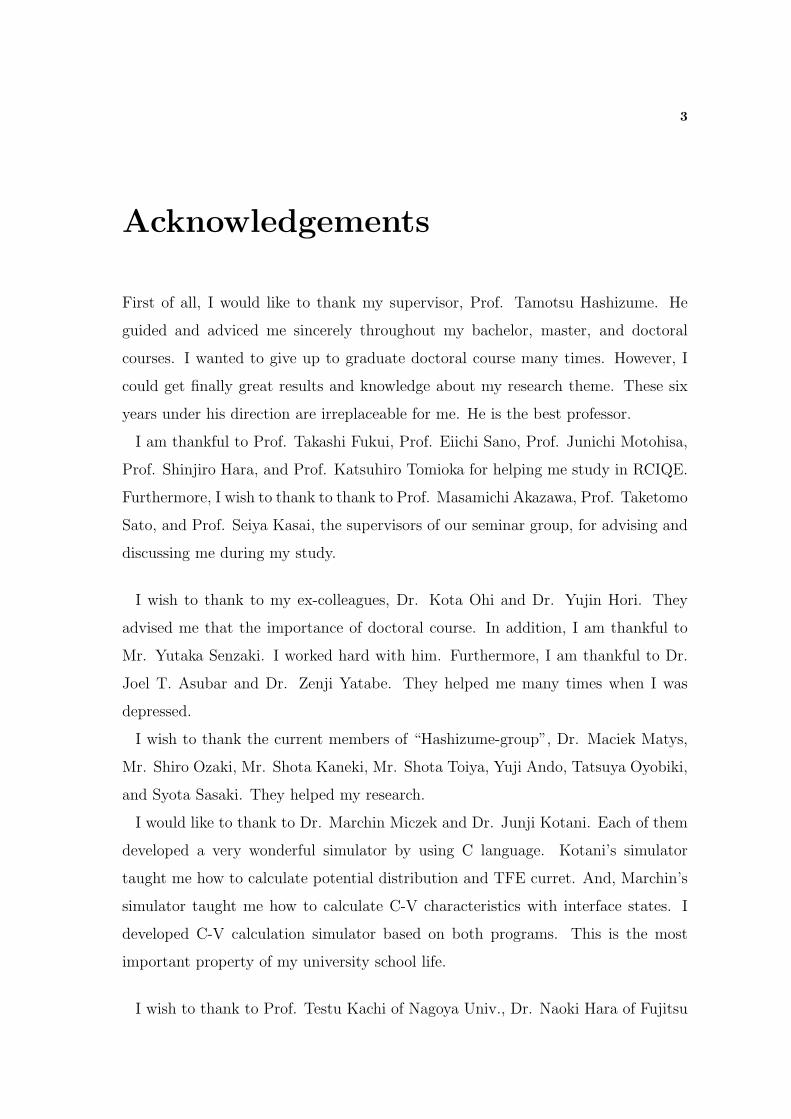
The volume of communication traffic has been increasing worldwide with the rapid
spread of smartphones in recent years. The global volume of communication traffic
is expected to reach 30×1018 bytes/month in 2020 as shown in Figure 1.1. Increases
in communication facilities, speed, and capacity are thus required.
Figure 1.1. Predicted global volume of mobile communication.
The frequency band used for mobile communication in Japan is 700 MHz–2 GHz.
8 Chapter 1 Introduction
However, 5 GHz will be used in future [1]. Increasing the communication frequency
can increase the speed and capacity of mobile communications. However, a dis-
advantage of using a high frequency in long-distance communication is the large
degradation in the atmosphere. In addition, obstacles such as buildings adversely
affect mobile communications. To solve these problems, it is necessary to improve
the power of communication amplifiers used in base stations.
There is another problem in backhaul, that is, the intermediate links between base
stations. The frequency band used for backhaul is extremely high, 40 to 50 GHz.
In addition, the frequency band used for backhaul depends on that used for mobile
communication.
1.1.2 Radars
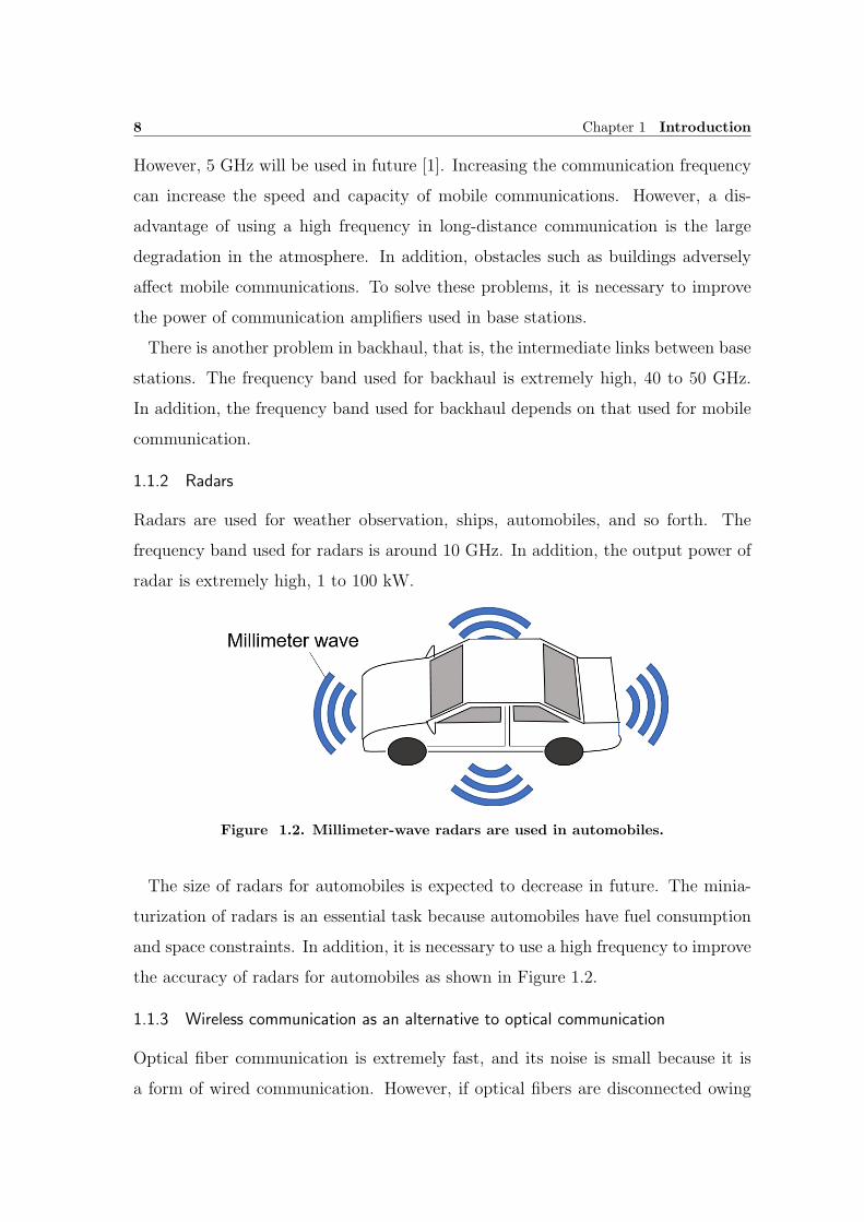
Radars are used for weather observation, ships, automobiles, and so forth. The
frequency band used for radars is around 10 GHz. In addition, the output power of
radar is extremely high, 1 to 100 kW.
Figure 1.2. Millimeter-wave radars are used in automobiles.
The size of radars for automobiles is expected to decrease in future. The minia-
turization of radars is an essential task because automobiles have fuel consumption
and space constraints. In addition, it is necessary to use a high frequency to improve
the accuracy of radars for automobiles as shown in Figure 1.2.
1.1.3 Wireless communication as an alternative to optical communication
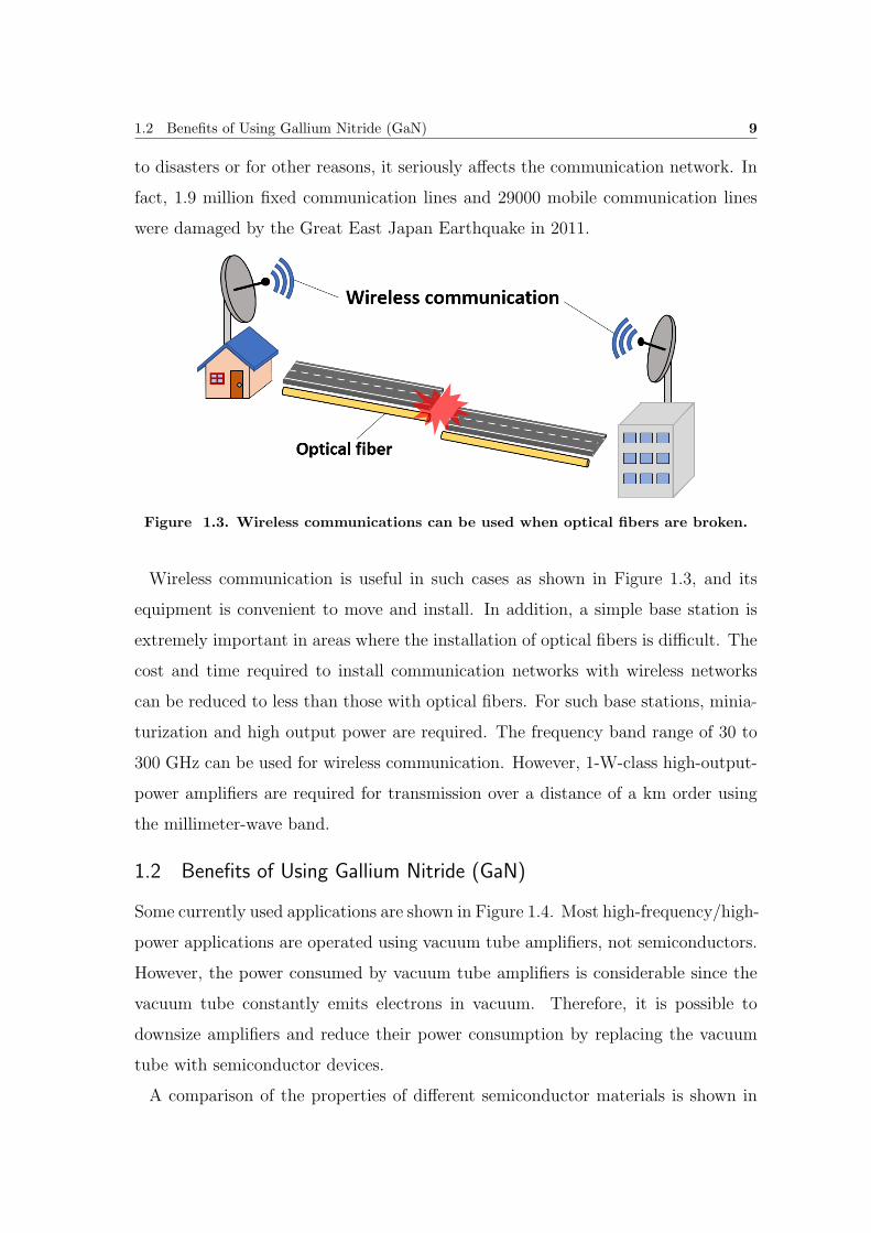
Optical fiber communication is extremely fast, and its noise is small because it is
a form of wired communication. However, if optical fibers are disconnected owing
1.2 Benefits of Using Gallium Nitride (GaN) 9
to disasters or for other reasons, it seriously affects the communication network. In
fact, 1.9 million fixed communication lines and 29000 mobile communication lines
were damaged by the Great East Japan Earthquake in 2011.
Figure 1.3. Wireless communications can be used when optical fibers are broken.
Wireless communication is useful in such cases as shown in Figure 1.3, and its
equipment is convenient to move and install. In addition, a simple base station is
extremely important in areas where the installation of optical fibers is difficult. The
cost and time required to install communication networks with wireless networks
can be reduced to less than those with optical fibers. For such base stations, minia-
turization and high output power are required. The frequency band range of 30 to
300 GHz can be used for wireless communication. However, 1-W-class high-output-
power amplifiers are required for transmission over a distance of a km order using
the millimeter-wave band.
1.2 Benefits of Using Gallium Nitride (GaN)
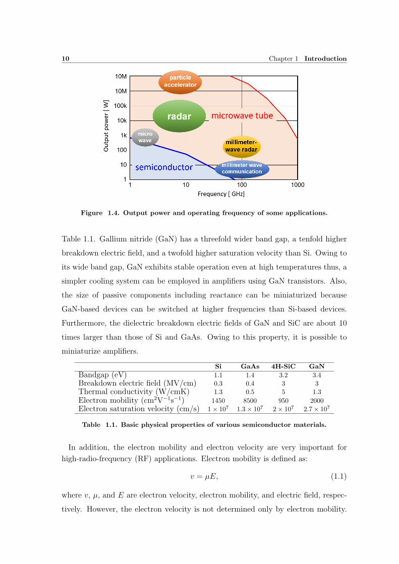
Some currently used applications are shown in Figure 1.4. Most high-frequency/high-
power applications are operated using vacuum tube amplifiers, not semiconductors.
However, the power consumed by vacuum tube amplifiers is considerable since the
vacuum tube constantly emits electrons in vacuum. Therefore, it is possible to
downsize amplifiers and reduce their power consumption by replacing the vacuum
tube with semiconductor devices.
A comparison of the properties of different semiconductor materials is shown in
10 Chapter 1 Introduction
Figure 1.4. Output power and operating frequency of some applications.
Table 1.1. Gallium nitride (GaN) has a threefold wider band gap, a tenfold higher
breakdown electric field, and a twofold higher saturation velocity than Si. Owing to
its wide band gap, GaN exhibits stable operation even at high temperatures thus, a
simpler cooling system can be employed in amplifiers using GaN transistors. Also,
the size of passive components including reactance can be miniaturized because
GaN-based devices can be switched at higher frequencies than Si-based devices.
Furthermore, the dielectric breakdown electric fields of GaN and SiC are about 10
times larger than those of Si and GaAs. Owing to this property, it is possible to
miniaturize amplifiers.
Si GaAs 4H-SiC GaN
Bandgap (eV) 1.1 1.4 3.2 3.4
Breakdown electric field (MV/cm) 0.3 0.4 3 3
Thermal conductivity (W/cmK) 1.3 0.5 5 1.3
Electron mobility (cm2V−1s−1) 1450 8500 950 2000
Electron saturation velocity (cm/s) 1× 10⁷ 1.3× 10⁷ 2× 10⁷ 2.7× 10⁷
Table 1.1. Basic physical properties of various semiconductor materials.
In addition, the electron mobility and electron velocity are very important for
high-radio-frequency (RF) applications. Electron mobility is defined as:
v = µE, (1.1)
where v, µ, and E are electron velocity, electron mobility, and electric field, respec-
tively. However, the electron velocity is not determined only by electron mobility.
1.2 Benefits of Using Gallium Nitride (GaN) 11
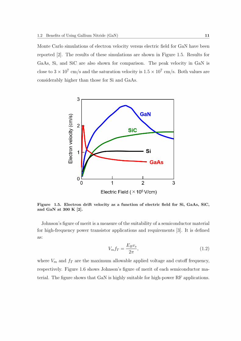
Monte Carlo simulations of electron velocity versus electric field for GaN have been
reported [2]. The results of these simulations are shown in Figure 1.5. Results for
GaAs, Si, and SiC are also shown for comparison. The peak velocity in GaN is
close to 3× 107 cm/s and the saturation velocity is 1.5× 107 cm/s. Both values are
considerably higher than those for Si and GaAs.
Figure 1.5. Electron drift velocity as a function of electric field for Si, GaAs, SiC,and GaN at 300 K [2].
Johnson’s figure of merit is a measure of the suitability of a semiconductor material
for high-frequency power transistor applications and requirements [3]. It is defined
as:
VmfT =EBvs2π
, (1.2)
where Vm and fT are the maximum allowable applied voltage and cutoff frequency,
respectively. Figure 1.6 shows Johnson’s figure of merit of each semiconductor ma-
terial. The figure shows that GaN is highly suitable for high-power RF applications.
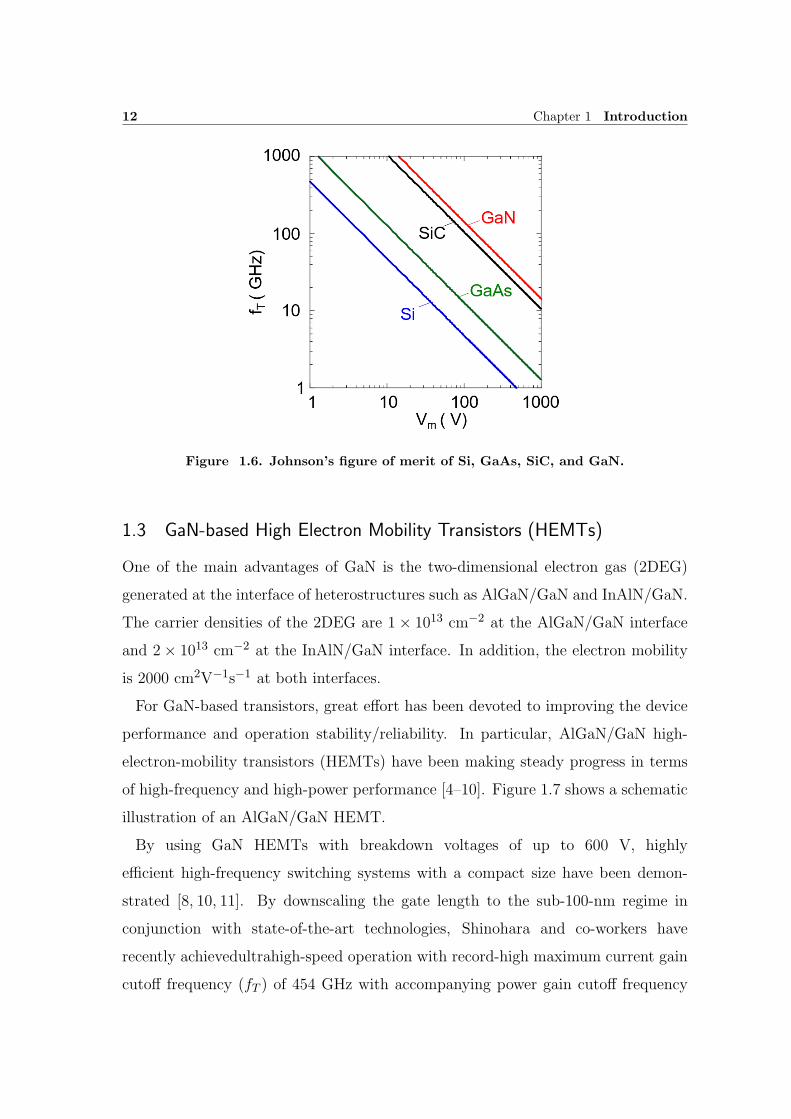
12 Chapter 1 Introduction
Figure 1.6. Johnson’s figure of merit of Si, GaAs, SiC, and GaN.
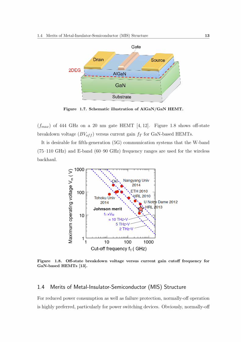
1.3 GaN-based High Electron Mobility Transistors (HEMTs)
One of the main advantages of GaN is the two-dimensional electron gas (2DEG)
generated at the interface of heterostructures such as AlGaN/GaN and InAlN/GaN.
The carrier densities of the 2DEG are 1× 1013 cm−2 at the AlGaN/GaN interface
and 2× 1013 cm−2 at the InAlN/GaN interface. In addition, the electron mobility
is 2000 cm2V−1s−1 at both interfaces.
For GaN-based transistors, great effort has been devoted to improving the device
performance and operation stability/reliability. In particular, AlGaN/GaN high-
electron-mobility transistors (HEMTs) have been making steady progress in terms
of high-frequency and high-power performance [4–10]. Figure 1.7 shows a schematic
illustration of an AlGaN/GaN HEMT.
By using GaN HEMTs with breakdown voltages of up to 600 V, highly
efficient high-frequency switching systems with a compact size have been demon-
strated [8, 10, 11]. By downscaling the gate length to the sub-100-nm regime in
conjunction with state-of-the-art technologies, Shinohara and co-workers have
recently achievedultrahigh-speed operation with record-high maximum current gain
cutoff frequency (fT ) of 454 GHz with accompanying power gain cutoff frequency
1.4 Merits of Metal-Insulator-Semiconductor (MIS) Structure 13
Figure 1.7. Schematic illustration of AlGaN/GaN HEMT.
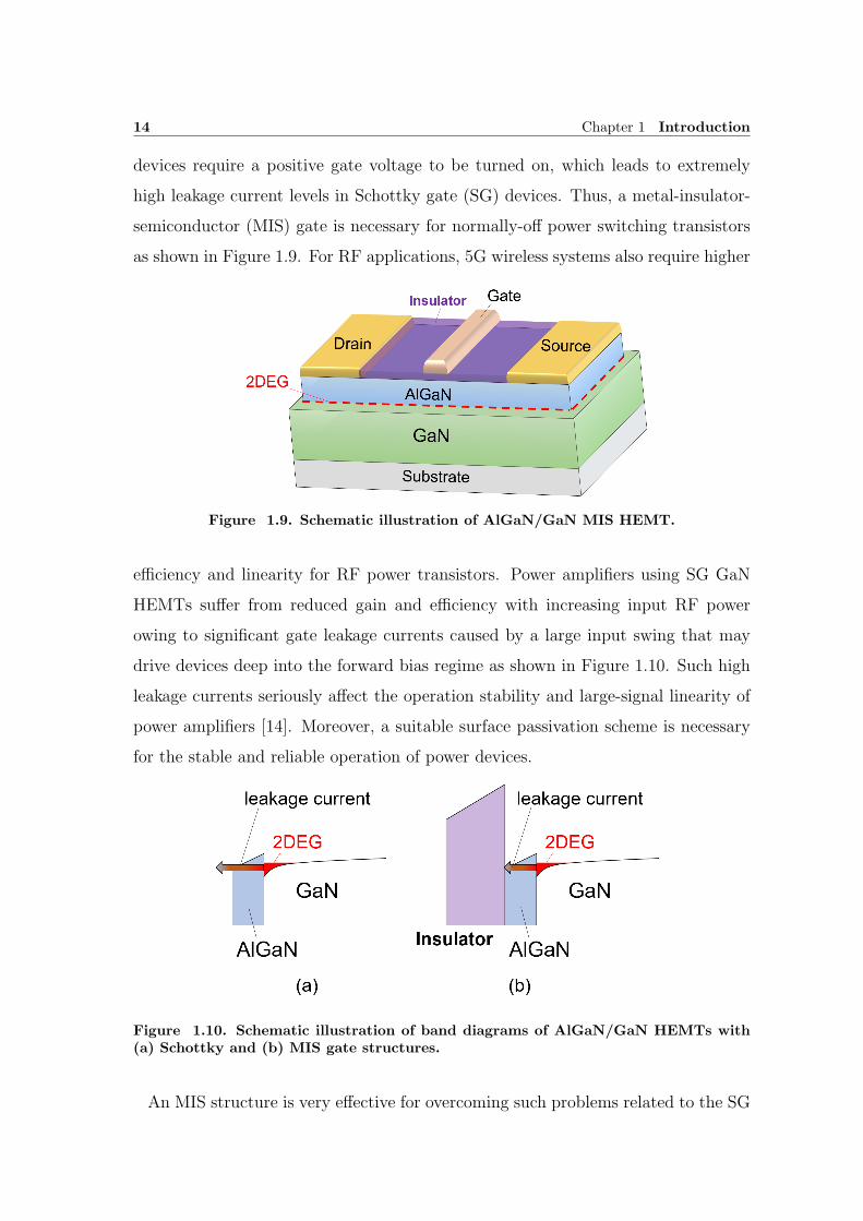
(fmax) of 444 GHz on a 20 nm gate HEMT [4, 12]. Figure 1.8 shows off-state
breakdown voltage (BVoff ) versus current gain fT for GaN-based HEMTs.
It is desirable for fifth-generation (5G) communication systems that the W-band
(75–110 GHz) and E-band (60–90 GHz) frequency ranges are used for the wireless
backhaul.
Figure 1.8. Off-state breakdown voltage versus current gain cutoff frequency forGaN-based HEMTs [13].
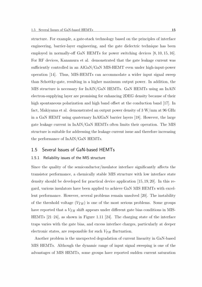
1.4 Merits of Metal-Insulator-Semiconductor (MIS) Structure
For reduced power consumption as well as failure protection, normally-off operation
is highly preferred, particularly for power switching devices. Obviously, normally-off
14 Chapter 1 Introduction
devices require a positive gate voltage to be turned on, which leads to extremely
high leakage current levels in Schottky gate (SG) devices. Thus, a metal-insulator-
semiconductor (MIS) gate is necessary for normally-off power switching transistors
as shown in Figure 1.9. For RF applications, 5G wireless systems also require higher
Figure 1.9. Schematic illustration of AlGaN/GaN MIS HEMT.
efficiency and linearity for RF power transistors. Power amplifiers using SG GaN
HEMTs suffer from reduced gain and efficiency with increasing input RF power
owing to significant gate leakage currents caused by a large input swing that may
drive devices deep into the forward bias regime as shown in Figure 1.10. Such high
leakage currents seriously affect the operation stability and large-signal linearity of
power amplifiers [14]. Moreover, a suitable surface passivation scheme is necessary
for the stable and reliable operation of power devices.
Figure 1.10. Schematic illustration of band diagrams of AlGaN/GaN HEMTs with(a) Schottky and (b) MIS gate structures.
An MIS structure is very effective for overcoming such problems related to the SG
1.5 Several Issues of GaN-based HEMTs 15
structure. For example, a gate-stack technology based on the principles of interface
engineering, barrier-layer engineering, and the gate dielectric technique has been
employed in normally-off GaN HEMTs for power switching devices [8, 10, 15, 16].
For RF devices, Kanamura et al. demonstrated that the gate leakage current was
sufficiently controlled in an AlGaN/GaN MIS-HEMT even under high-input-power
operation [14]. Thus, MIS-HEMTs can accommodate a wider input signal sweep
than Schottky-gate, resulting in a higher maximum output power. In addition, the
MIS structure is necessary for InAlN/GaN HEMTs. GaN HEMTs using an InAlN
electron-supplying layer are promising for enhancing 2DEG density because of their
high spontaneous polarization and high band offset at the conduction band [17]. In
fact, Makiyama et al. demonstrated an output power density of 3 W/mm at 96 GHz
in a GaN HEMT using quaternary InAlGaN barrier layers [18]. However, the large
gate leakage current in InAlN/GaN HEMTs often limits their operation. The MIS
structure is suitable for addressing the leakage current issue and therefore increasing
the performance of InAlN/GaN HEMTs.
1.5 Several Issues of GaN-based HEMTs
1.5.1 Reliability issues of the MIS structure
Since the quality of the semiconductor/insulator interface significantly affects the
transistor performance, a chemically stable MIS structure with low interface state
density should be developed for practical device application [15, 19, 20]. In this re-
gard, various insulators have been applied to achieve GaN MIS HEMTs with excel-
lent performance. However, several problems remain unsolved [20]. The instability
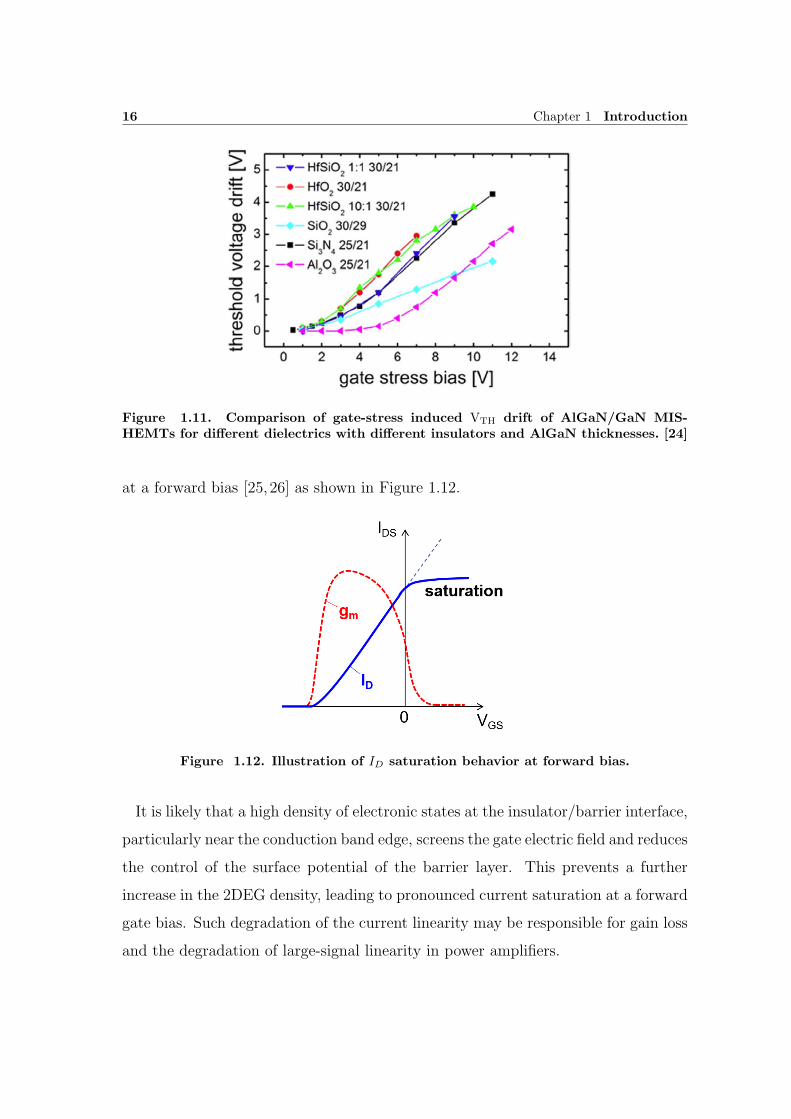
of the threshold voltage (VTH) is one of the most serious problems. Some groups
have reported that a VTH shift appears under different gate bias conditions in MIS-
HEMTs [21–24], as shown in Figure 1.11 [24]. The charging state of the interface
traps varies with the gate bias, and excess interface charges, particularly at deeper
electronic states, are responsible for such VTH fluctuation.
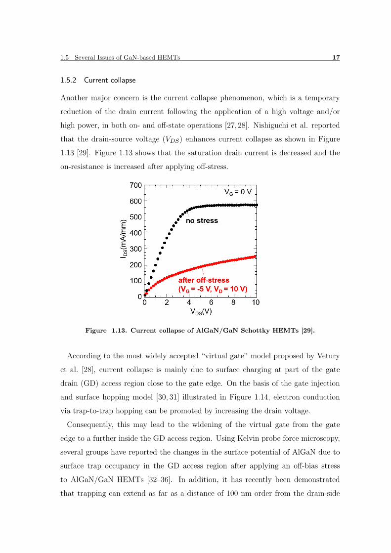
Another problem is the unexpected degradation of current linearity in GaN-based
MIS HEMTs. Although the dynamic range of input signal sweeping is one of the
advantages of MIS HEMTs, some groups have reported sudden current saturation
16 Chapter 1 Introduction
Figure 1.11. Comparison of gate-stress induced VTH drift of AlGaN/GaN MIS-HEMTs for different dielectrics with different insulators and AlGaN thicknesses. [24]
at a forward bias [25,26] as shown in Figure 1.12.
Figure 1.12. Illustration of ID saturation behavior at forward bias.
It is likely that a high density of electronic states at the insulator/barrier interface,
particularly near the conduction band edge, screens the gate electric field and reduces
the control of the surface potential of the barrier layer. This prevents a further
increase in the 2DEG density, leading to pronounced current saturation at a forward
gate bias. Such degradation of the current linearity may be responsible for gain loss
and the degradation of large-signal linearity in power amplifiers.
1.5 Several Issues of GaN-based HEMTs 17
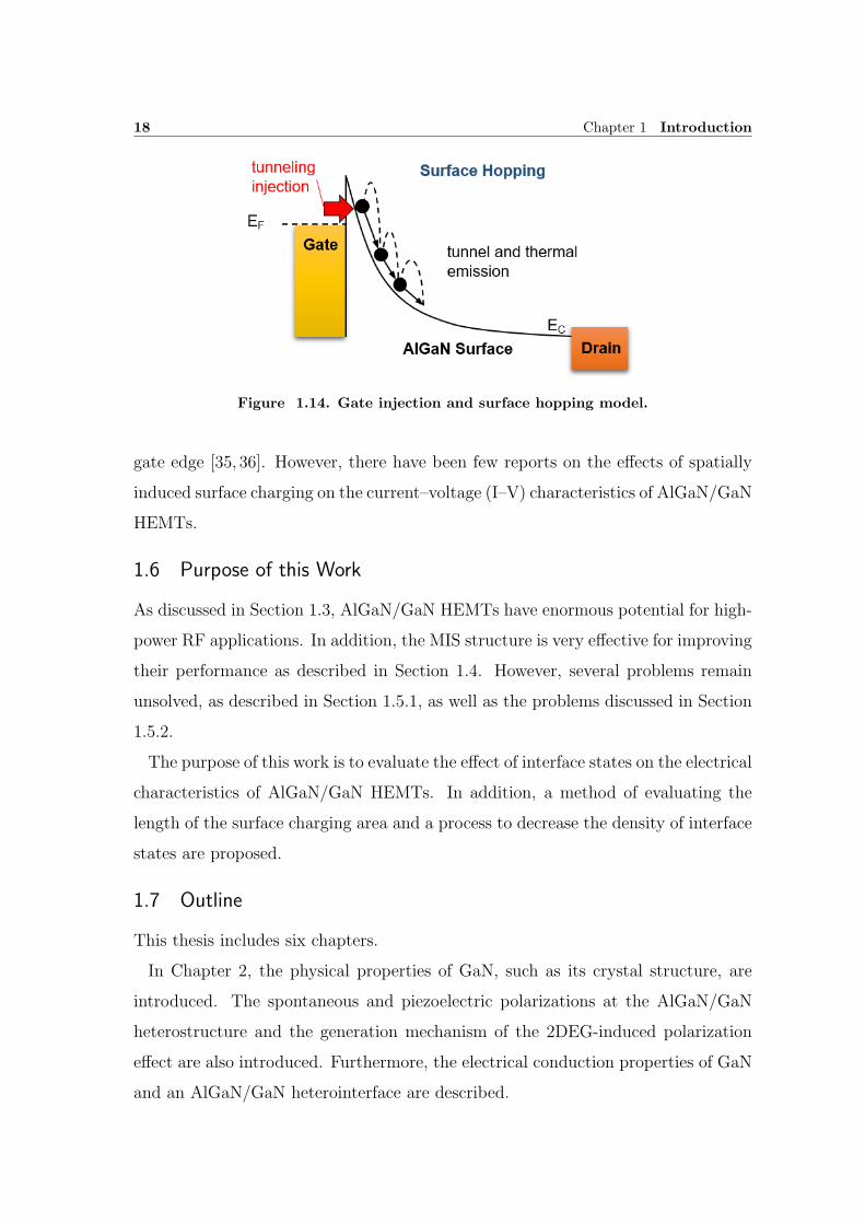
1.5.2 Current collapse
Another major concern is the current collapse phenomenon, which is a temporary
reduction of the drain current following the application of a high voltage and/or
high power, in both on- and off-state operations [27, 28]. Nishiguchi et al. reported
that the drain-source voltage (VDS) enhances current collapse as shown in Figure
1.13 [29]. Figure 1.13 shows that the saturation drain current is decreased and the
on-resistance is increased after applying off-stress.
Figure 1.13. Current collapse of AlGaN/GaN Schottky HEMTs [29].
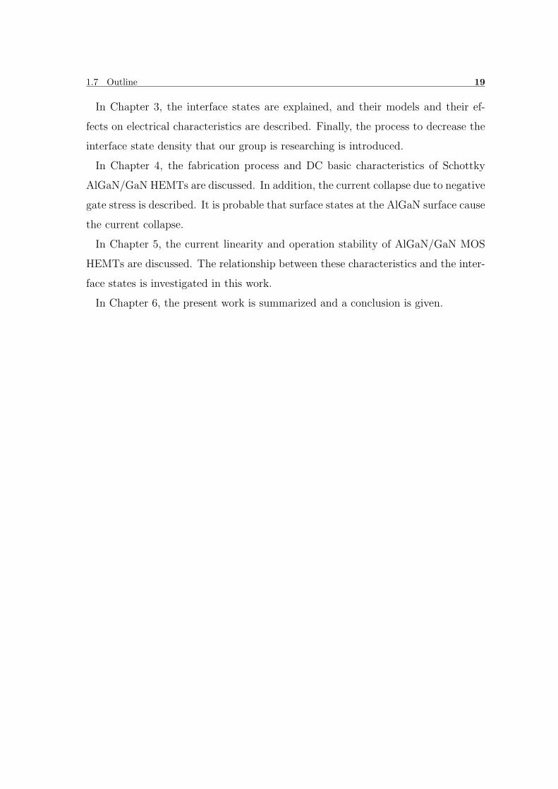
According to the most widely accepted “virtual gate” model proposed by Vetury
et al. [28], current collapse is mainly due to surface charging at part of the gate
drain (GD) access region close to the gate edge. On the basis of the gate injection
and surface hopping model [30, 31] illustrated in Figure 1.14, electron conduction
via trap-to-trap hopping can be promoted by increasing the drain voltage.
Consequently, this may lead to the widening of the virtual gate from the gate
edge to a further inside the GD access region. Using Kelvin probe force microscopy,
several groups have reported the changes in the surface potential of AlGaN due to
surface trap occupancy in the GD access region after applying an off-bias stress
to AlGaN/GaN HEMTs [32–36]. In addition, it has recently been demonstrated
that trapping can extend as far as a distance of 100 nm order from the drain-side
18 Chapter 1 Introduction
Figure 1.14. Gate injection and surface hopping model.
gate edge [35, 36]. However, there have been few reports on the effects of spatially
induced surface charging on the current–voltage (I–V) characteristics of AlGaN/GaN
HEMTs.
1.6 Purpose of this Work
As discussed in Section 1.3, AlGaN/GaN HEMTs have enormous potential for high-
power RF applications. In addition, the MIS structure is very effective for improving
their performance as described in Section 1.4. However, several problems remain
unsolved, as described in Section 1.5.1, as well as the problems discussed in Section
1.5.2.
The purpose of this work is to evaluate the effect of interface states on the electrical
characteristics of AlGaN/GaN HEMTs. In addition, a method of evaluating the
length of the surface charging area and a process to decrease the density of interface
states are proposed.
1.7 Outline
This thesis includes six chapters.
In Chapter 2, the physical properties of GaN, such as its crystal structure, are
introduced. The spontaneous and piezoelectric polarizations at the AlGaN/GaN
heterostructure and the generation mechanism of the 2DEG-induced polarization
effect are also introduced. Furthermore, the electrical conduction properties of GaN
and an AlGaN/GaN heterointerface are described.
1.7 Outline 19
In Chapter 3, the interface states are explained, and their models and their ef-
fects on electrical characteristics are described. Finally, the process to decrease the
interface state density that our group is researching is introduced.
In Chapter 4, the fabrication process and DC basic characteristics of Schottky
AlGaN/GaN HEMTs are discussed. In addition, the current collapse due to negative
gate stress is described. It is probable that surface states at the AlGaN surface cause
the current collapse.
In Chapter 5, the current linearity and operation stability of AlGaN/GaN MOS
HEMTs are discussed. The relationship between these characteristics and the inter-
face states is investigated in this work.
In Chapter 6, the present work is summarized and a conclusion is given.

21
References
[1] T. Hashizume, K. Nishiguchi, S. Kaneki, J. Kuzmik, and Z. Yatabe, Mater. Sci.
Semicond. Process. (2017).
[2] S. C. Jain, M. Willander, J. Narayan, and R. Van Overstraeten, J. Appl. Phys.
87, 965 (2000).
[3] E. O. Johnson, RCA Rev. 26, 163 (1965).
[4] K. Shinohara, D.C. Regan, Y. Tang, A. L. Corrion, D.F. Brown, J.C. Wong,
J.F. Robinson, H.H. Fung, A. Schmitz, T.C. Oh, S.J. Kim, P.S. Chen, R.G.
Nagele, A.D. Margomenos, and M. Micovic, IEEE Trans. Electron Devices 60,
2983 (2013).
[5] D.S. Lee, Z. Liu, and T. Palacios, Jpn. J. Appl. Phys. 53, 100212 (2014).
[6] T. Ueda, M. Ishida, T. Tanaka, and D. Ueda, Jpn. J. Appl. Phys. 53, 100214
(2014).
[7] T. Kachi, Jpn. J. Appl. Phys. 53, 100210 (2014).
[8] F. Roccaforte, P. Fiorenza, G. Greco, R.L. Nigro, F. Giannazzo, A. Patti, and
M. Saggio, Phys. Status Solidi A 211, 2063 (2014).
[9] M. Kuzuhara and H. Tokuda, IEEE Trans. Electron Devices 62, 405 (2015).
[10] K.J. Chen, O. Haeberlen, A. Lidow, C. l. Tsai, T. Ueda, Y. Uemoto, and Y.
Wu, IEEE Trans. Electron Devices 64, 779 (2017).
[11] E. A. Jones, F. Wang, and D. Costinett, IEEE J. Emerging and Selected Topics
in Power Electronics 4, 707 (2016).
[12] Y. Tang, K. Shinohara, D. Regan, A. Corrion, D. Brown, J. Wong, A. Schmitz,
H. Fung, S. Kim, and M. Micovic, IEEE Electron Device Lett. 36, 549 (2015).
[13] K. Kobayashi, S. Hatakeyama, T. Yoshida, Y. Yabe, D. Piedra, T. Palacios, T.
Otsuji, and T. Suemitsu, Appl. Phys. Express 7, 096501 (2014).
[14] M. Kanamura, T. Kikkawa, T. Iwai, K. Imanishi, T. Kubo, and K. Joshin,
IEDM Tech. Dig., 2005, p. 572.
22 References
[15] F. Roccaforte, P. Fiorenza, G. Greco, M. Vivona, R. L. Nigro, F. Giannazzo,
A. Patti, and M. Saggio, Appl. Surf. Sci. 301, 9 (2014).
[16] S. Yang, S. Liu, C. Liu, M. Hua, and K.J. Chen, Semicond. Sci. Technol. 31,
024001 (2016).
[17] J. Kuzmik, IEEE Electron Device Lett. 22, 510 (2001).
[18] K. Makiyama, S. Ozaki, T. Ohki, N. Okamoto, Y. Minoura, Y. Niida, Y. Ka-
mada, K. Joshin, K. Watanabe, and Y. Miyamoto, IEDM Tech. Dig., 2015, p.
213.
[19] Z. Yatabe, Y. Hori, W. Ma, J.T. Asubar, M. Akazawa, T. Sato, and T.
Hashizume, Jpn. J. Appl. Phys. 53, 100213 (2014).
[20] Z. Yatabe, J.T. Asubar, and T. Hashizume, J. Phys. D 49, 393001 (2016).
[21] Y. Lu, S. Yang, Q. Jiang, Z. Tang, B. Li, and K.J. Chen, Phys. Status Solidi C
10, 1397 (2013).
[22] M. Tapajna, M. Jurkovic, L. Valik, S. Hascik, D. Gregusova, F. Brunner, E.-M.
Cho, and J. Kuzmik, Appl. Phys. Lett. 102, 243509 (2013).
[23] D.W. Johnson, R.T.P. Lee, R.J.W. Hill, M.H. Wong, G. Bersuker, E.L. Piner,
P.D. Kirsch, and H.R. Harris, IEEE Trans. Electron Devices 60, 3197 (2013).
[24] P. Lagger, P. Steinschifter, M. Reiner, M. Stadtmuller, G. Denifl, A. Naumann,
J. Muller, L. Wilde, J. Sundqvist, D. Pogany, and C. Ostermaier, Appl. Phys.
Lett. 105, 033512 (2014).
[25] Z. Zhang, W. Li, K. Fu, G. Yu, X. Zhang, Y. Zhao, S. Sun, L. Song, X. Deng,
Z. Xing, L. Yang, R. Ji, C. Zeng, Y. Fan, Z. Dong, Y. Cai, and B. Zhang, IEEE
Electron Device Lett. 38, 236 (2017).
[26] X. Lu, K. Yu, H. Jiang, A. Zhang, and K.M. Lau, IEEE Trans. Electron Devices
64, 824 (2017).
[27] M. A. Khan, M. S. Shur, Q. C. Chen, and J. N. Kuznia, Electron. Lett. 30,
2175 (1994).
[28] R. Vetury, N. Q. Zhang, S. Keller, and U. K. Mishra, IEEE Trans. Electron
Devices 48, 560 (2001).
[29] K. Nishiguchi, J. T. Asubar, and T. Hashizume, Jpn. J. Appl. Phys. 53, 070301
(2014).
23
[30] R. J. Trew, D. S. Green, and J. B. Shealy, IEEE Microwave Mag. 10 [4], 116
(2009).
[31] J. Kotani, M. Tajima, S. Kasai, and T. Hashizume, Appl. Phys. Lett. 91, 093501
(2007).
[32] G. Koley, V. Tilak, L. F. Eastman, and M. G. Spencer, IEEE Trans. Electron
Devices 50, 886 (2003).
[33] K. Nakagami, Y. Ohno, S. Kishimoto, K. Maezawa, and T. Mizutani, Appl.
Phys. Lett. 85, 6028 (2004).
[34] S. Kamiya, M. Iwami, T. Tsuchiya, M. Kurouchi, J. Kikawa, T. Yamada, A.
Wakejima, H. Miyamoto, A. Suzuki, A. Hinoki, T. Araki, and Y. Nanishi, Appl.
Phys. Lett. 90, 213511 (2007).
[35] S. DasGupta, L. B. Biedermann, M. Sun, R. Kaplar, M. Marinella, K. R.
Zavadil, S. Atcitty, and T. Palacios, Appl. Phys. Lett. 101, 243506 (2012).
[36] D. W. Cardwell, A. R. Arehart, C. Poblenz, Y. Pei, J. S. Speck, U. K. Mishra,
S. A. Ringel, and J. P. Pelz, Appl. Phys. Lett. 100, 193507 (2012).

25
Chapter 2
Physical properties of GaN
2.1 Basic Properties of III-N Semiconductor Materials
2.1.1 Crystal Structure
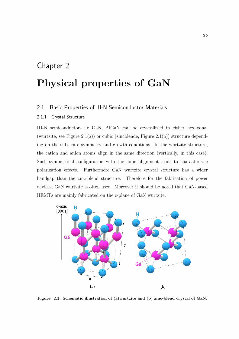
III-N semiconductors i.e GaN, AlGaN can be crystallized in either hexagonal
(wurtzite, see Figure 2.1(a)) or cubic (zincblende, Figure 2.1(b)) structure depend-
ing on the substrate symmetry and growth conditions. In the wurtzite structure,
the cation and anion atoms align in the same direction (vertically, in this case).
Such symmetrical configuration with the ionic alignment leads to characteristic
polarization effects. Furthermore GaN wurtzite crystal structure has a wider
bandgap than the zinc-blend structure. Therefore for the fabrication of power
devices, GaN wurtzite is often used. Moreover it should be noted that GaN-based
HEMTs are mainly fabricated on the c-plane of GaN wurtzite.
Figure 2.1. Schematic illustration of (a)wurtzite and (b) zinc-blend crystal of GaN.
26 Chapter 2 Physical properties of GaN
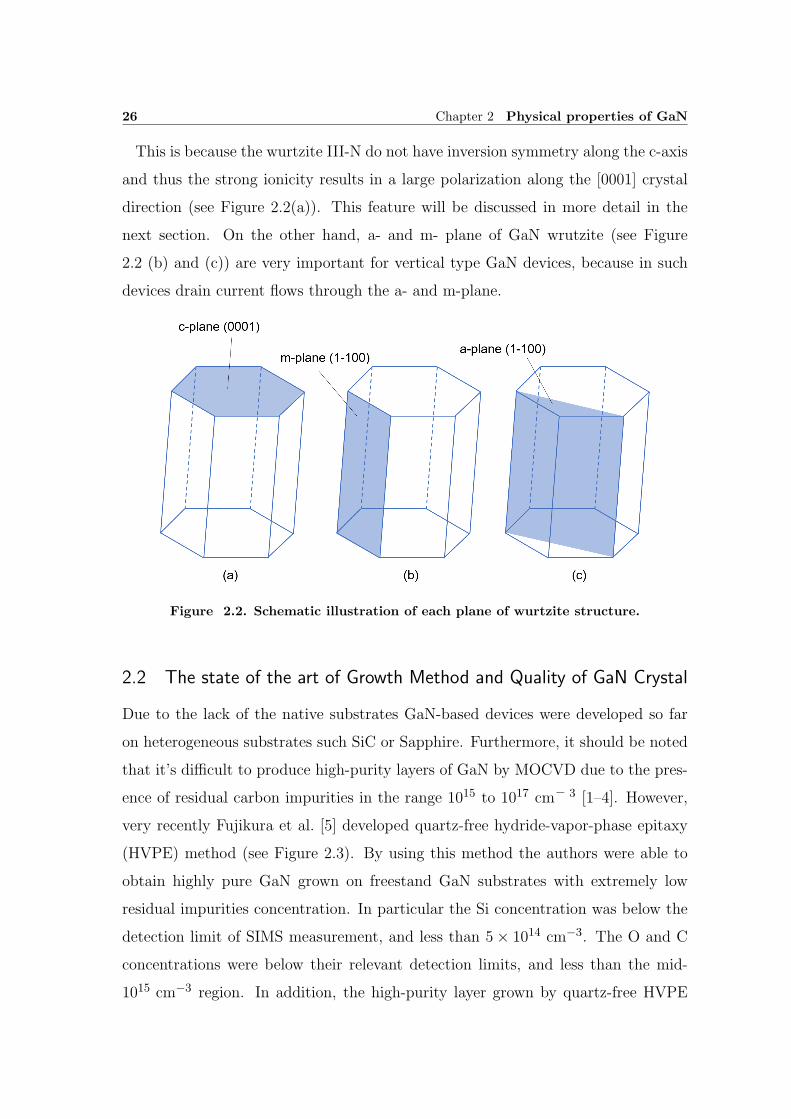
This is because the wurtzite III-N do not have inversion symmetry along the c-axis
and thus the strong ionicity results in a large polarization along the [0001] crystal
direction (see Figure 2.2(a)). This feature will be discussed in more detail in the
next section. On the other hand, a- and m- plane of GaN wrutzite (see Figure
2.2 (b) and (c)) are very important for vertical type GaN devices, because in such
devices drain current flows through the a- and m-plane.
Figure 2.2. Schematic illustration of each plane of wurtzite structure.
2.2 The state of the art of Growth Method and Quality of GaN Crystal
Due to the lack of the native substrates GaN-based devices were developed so far
on heterogeneous substrates such SiC or Sapphire. Furthermore, it should be noted
that it’s difficult to produce high-purity layers of GaN by MOCVD due to the pres-
ence of residual carbon impurities in the range 1015 to 1017 cm- 3 [1–4]. However,
very recently Fujikura et al. [5] developed quartz-free hydride-vapor-phase epitaxy
(HVPE) method (see Figure 2.3). By using this method the authors were able to
obtain highly pure GaN grown on freestand GaN substrates with extremely low
residual impurities concentration. In particular the Si concentration was below the
detection limit of SIMS measurement, and less than 5× 1014 cm−3. The O and C
concentrations were below their relevant detection limits, and less than the mid-
1015 cm−3 region. In addition, the high-purity layer grown by quartz-free HVPE
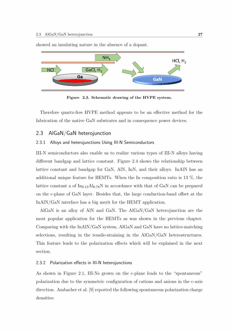
2.3 AlGaN/GaN heterojunction 27
showed an insulating nature in the absence of a dopant.
Figure 2.3. Schematic drawing of the HVPE system.
Therefore quartz-free HVPE method appears to be an effective method for the
fabrication of the native GaN substrates and in consequence power devices.
2.3 AlGaN/GaN heterojunction
2.3.1 Alloys and heterojunctions Using III-N Semiconductors
III-N semiconductors also enable us to realize various types of III-N alloys having
different bandgap and lattice constant. Figure 2.4 shows the relationship between
lattice constant and bandgap for GaN, AlN, InN, and their alloys. InAlN has an
additional unique feature for HEMTs. When the In composition ratio is 13 %, the
lattice constant a of In0.13Al0.78N in accordance with that of GaN can be prepared
on the c-plane of GaN layer. Besides that, the large conduction-band offset at the
InAlN/GaN interface has a big merit for the HEMT application.
AlGaN is an alloy of AlN and GaN. The AlGaN/GaN heterojunction are the
most popular application for the HEMTs as was shown in the previous chapter.
Comparing with the InAlN/GaN system, AlGaN and GaN have no lattice-matching
selections, resulting in the tensile-straining in the AlGaN/GaN heterostructures.
This feature leads to the polarization effects which will be explained in the next
section.
2.3.2 Polarization effects in III-N heterojunctions
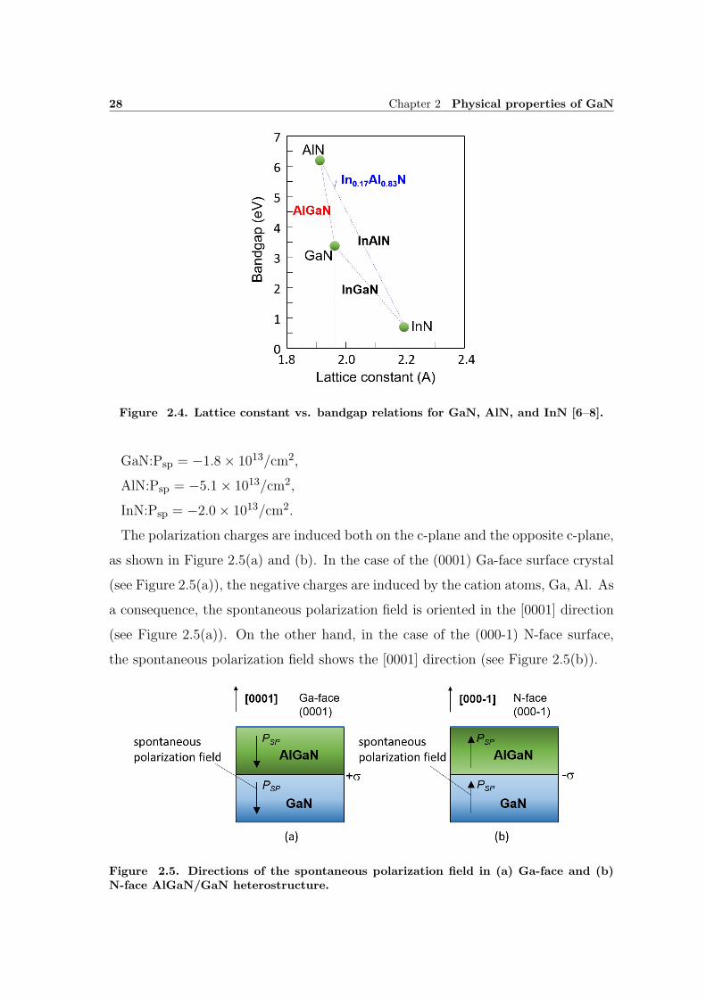
As shown in Figure 2.1, III-Ns grown on the c-plane leads to the “spontaneous”
polarization due to the symmetric configuration of cations and anions in the c-axis
direction. Ambacher et al. [9] reported the following spontaneous polarization charge
densities:
28 Chapter 2 Physical properties of GaN
Figure 2.4. Lattice constant vs. bandgap relations for GaN, AlN, and InN [6–8].
GaN:Psp = −1.8× 10¹³/cm2,
AlN:Psp = −5.1× 10¹³/cm2,
InN:Psp = −2.0× 10¹³/cm2.
The polarization charges are induced both on the c-plane and the opposite c-plane,
as shown in Figure 2.5(a) and (b). In the case of the (0001) Ga-face surface crystal
(see Figure 2.5(a)), the negative charges are induced by the cation atoms, Ga, Al. As
a consequence, the spontaneous polarization field is oriented in the [0001] direction
(see Figure 2.5(a)). On the other hand, in the case of the (000-1) N-face surface,
the spontaneous polarization field shows the [0001] direction (see Figure 2.5(b)).
Figure 2.5. Directions of the spontaneous polarization field in (a) Ga-face and (b)N-face AlGaN/GaN heterostructure.
2.3 AlGaN/GaN heterojunction 29
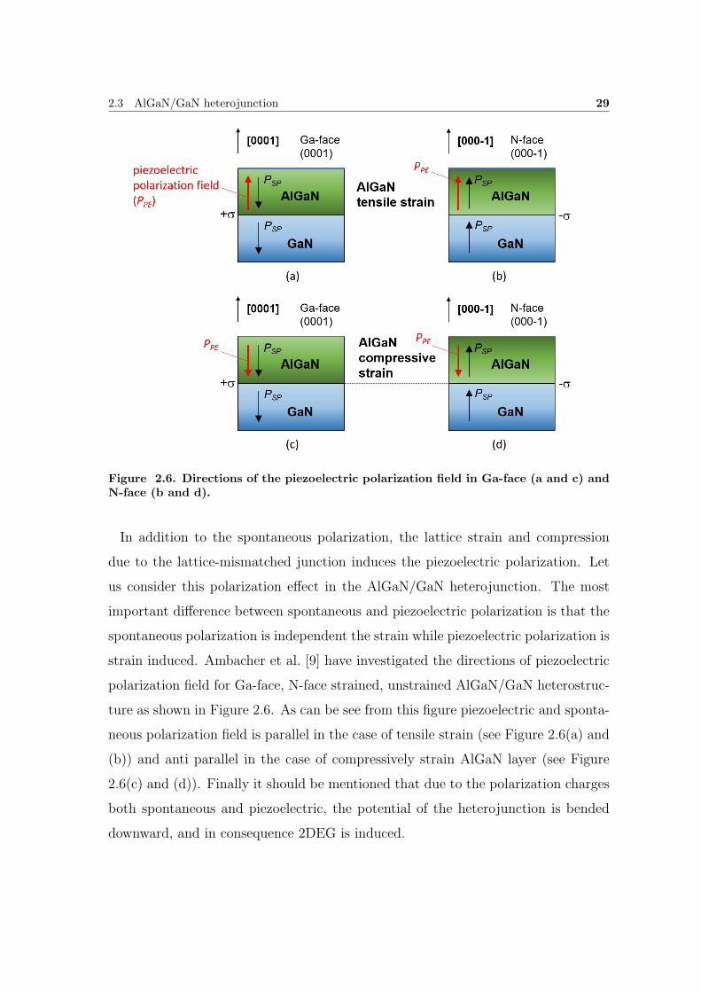
Figure 2.6. Directions of the piezoelectric polarization field in Ga-face (a and c) andN-face (b and d).
In addition to the spontaneous polarization, the lattice strain and compression
due to the lattice-mismatched junction induces the piezoelectric polarization. Let
us consider this polarization effect in the AlGaN/GaN heterojunction. The most
important difference between spontaneous and piezoelectric polarization is that the
spontaneous polarization is independent the strain while piezoelectric polarization is
strain induced. Ambacher et al. [9] have investigated the directions of piezoelectric
polarization field for Ga-face, N-face strained, unstrained AlGaN/GaN heterostruc-
ture as shown in Figure 2.6. As can be see from this figure piezoelectric and sponta-
neous polarization field is parallel in the case of tensile strain (see Figure 2.6(a) and
(b)) and anti parallel in the case of compressively strain AlGaN layer (see Figure
2.6(c) and (d)). Finally it should be mentioned that due to the polarization charges
both spontaneous and piezoelectric, the potential of the heterojunction is bended
downward, and in consequence 2DEG is induced.
30 Chapter 2 Physical properties of GaN
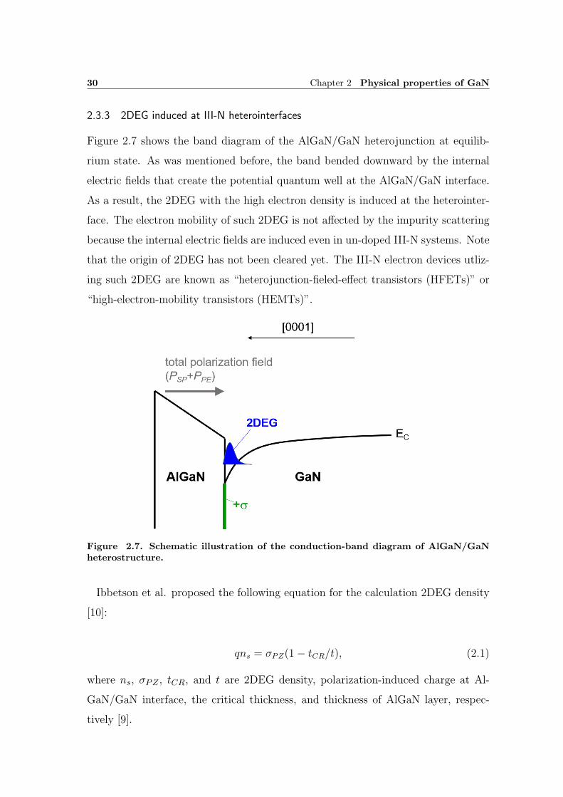
2.3.3 2DEG induced at III-N heterointerfaces
Figure 2.7 shows the band diagram of the AlGaN/GaN heterojunction at equilib-
rium state. As was mentioned before, the band bended downward by the internal
electric fields that create the potential quantum well at the AlGaN/GaN interface.
As a result, the 2DEG with the high electron density is induced at the heterointer-
face. The electron mobility of such 2DEG is not affected by the impurity scattering
because the internal electric fields are induced even in un-doped III-N systems. Note
that the origin of 2DEG has not been cleared yet. The III-N electron devices utliz-
ing such 2DEG are known as “heterojunction-fieled-effect transistors (HFETs)” or
“high-electron-mobility transistors (HEMTs)”.
Figure 2.7. Schematic illustration of the conduction-band diagram of AlGaN/GaNheterostructure.
Ibbetson et al. proposed the following equation for the calculation 2DEG density
[10]:
qns = σPZ(1− tCR/t), (2.1)
where ns, σPZ , tCR, and t are 2DEG density, polarization-induced charge at Al-
GaN/GaN interface, the critical thickness, and thickness of AlGaN layer, respec-
tively [9].
2.3 AlGaN/GaN heterojunction 31
The spontaneous polarization of AlGaN is calculated as follows:
PAlxGa1−xNSP = PAlN
SP x+ PGaNSP (1− x), (2.2)
where PAlNSP and PGaN
SP are spontaneous polarization of AlN and GaN, respectively.
The difference between spontaneous polarization of AlxGa1−xN and GaN ∆PSP is
calculated as follows:
∆PSP = PAlxGa1−xNSP − PGaN
SP . (2.3)
In order to obtain ∆PSP , it is necessary first calculated lattice constants. The
lattice constant of AlGaN can be calculated as follows:
aAlxGa1−xN = aAlNx+ aGaN(1− x), (2.4)
where aAlN and aGaN are a-lattice constants of AlN and GaN, respectively.
The elastic constant of AlGaN is calculated as follows:
C13(AlxGa1−xN) = C13(AlN)x+ C13(GaN)(1− x), (2.5)
C33(AlxGa1−xN) = C33(AlN)x+ C33(GaN)(1− x), (2.6)
where C13,33(AlN,GaN) are elastic constants of AlN and GaN, respectively.
The piezoelectric constant of AlGaN is calculated as follows:
e13(AlxGa1−xN) = e13(AlN)x+ e13(GaN)(1− x), (2.7)
e33(AlxGa1−xN) = e33(AlN)x+ e33(GaN)(1− x), (2.8)
where e13,33(AlN,GaN) are piezoelectric constants of AlN and GaN, respectively.
Using equation 2.2–2.8, the piezoelectric polarization charge can be calculated as
follows:
PAlxGa1−xNPE = 2(
aGaN − aAlxGa1−xN
aAlxGa1−xN)(e31(AlxGa1−xN) − e33(AlxGa1−xN)
C13(AlxGa1−xN)
C33(AlxGa1−xN)) (2.9)
The total polarization sheet charge density is defined by:
Ptotal = PAlxGa1−xNPE +∆PSP . (2.10)
For the Al composition equal to 20 %, Ptotal is 1.13 × 1013 cm−2, which is one
order of magnitude higher than the inversion carrier densities at Si and SiC MOS
interfaces.
Using In0.17Al0.83N as a barrier layer of HEMTs, the lattice-matched InAlN/GaN
heterojunction shows the PPE of zero. However, the higher PSP of the InAlN gives
32 Chapter 2 Physical properties of GaN
C33(GPa) C13(GPz) e33(Cm−2) e31(Cm
−2)GaN 415a 83a 0.65b −0.33b
AlN 373a 108a 1.55c −0.58c
aRef. [11], bRef. [12], cRef. [13]
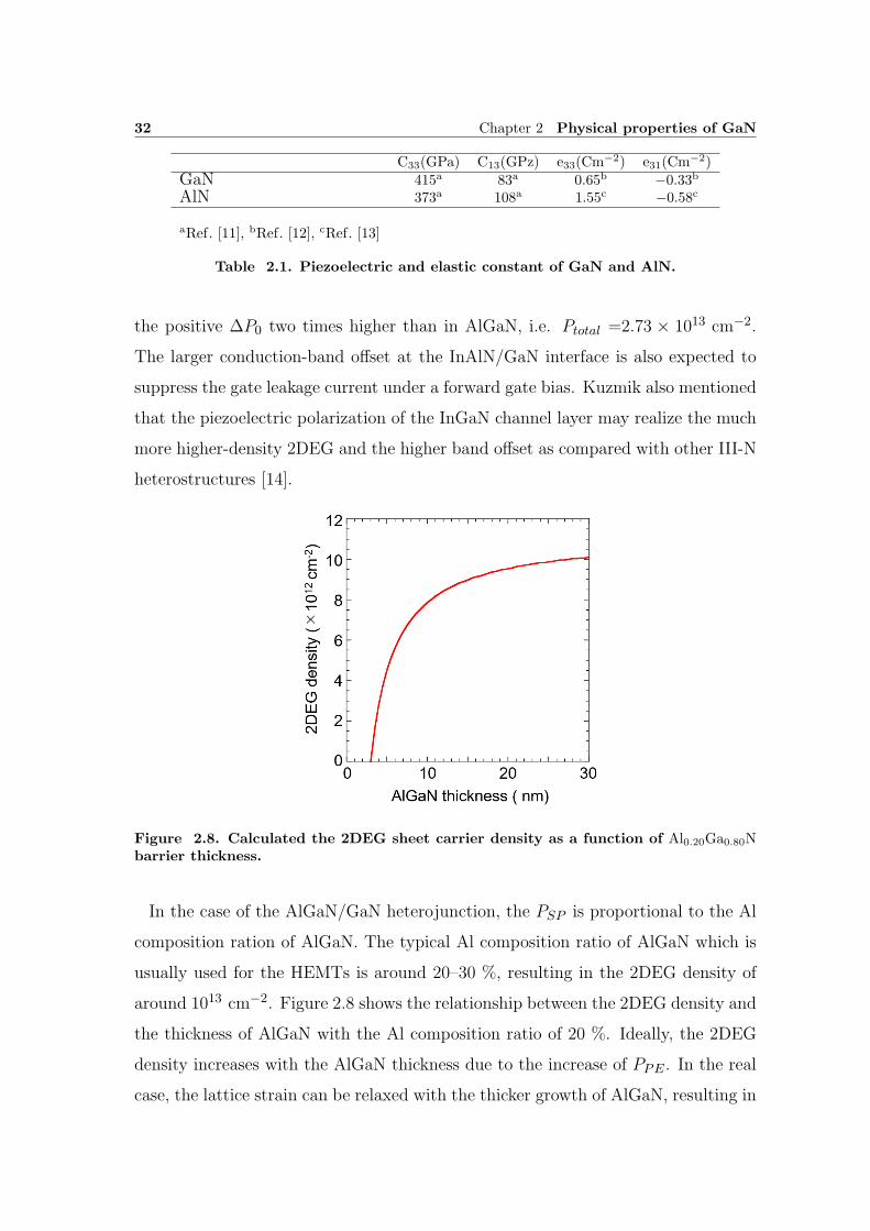
Table 2.1. Piezoelectric and elastic constant of GaN and AlN.
the positive ∆P0 two times higher than in AlGaN, i.e. Ptotal =2.73 × 1013 cm−2.
The larger conduction-band offset at the InAlN/GaN interface is also expected to
suppress the gate leakage current under a forward gate bias. Kuzmik also mentioned
that the piezoelectric polarization of the InGaN channel layer may realize the much
more higher-density 2DEG and the higher band offset as compared with other III-N
heterostructures [14].
Figure 2.8. Calculated the 2DEG sheet carrier density as a function of Al0.20Ga0.80Nbarrier thickness.
In the case of the AlGaN/GaN heterojunction, the PSP is proportional to the Al
composition ration of AlGaN. The typical Al composition ratio of AlGaN which is
usually used for the HEMTs is around 20–30 %, resulting in the 2DEG density of
around 1013 cm−2. Figure 2.8 shows the relationship between the 2DEG density and
the thickness of AlGaN with the Al composition ratio of 20 %. Ideally, the 2DEG
density increases with the AlGaN thickness due to the increase of PPE . In the real
case, the lattice strain can be relaxed with the thicker growth of AlGaN, resulting in
2.3 AlGaN/GaN heterojunction 33
the saturation of the 2DEG density. Furthermore, the thinner AlGaN also relaxes
the compression of itself, leading to decrease of PPE . As a consequence, when ∆P0
is zero, the heterojunction system does not create the 2DEG channel. Therefore in
the case of the AlGaN/GaN heterostructure, the 2DEG density can be modulated
by the Al composition ration and the thickness of AlGaN barrier layer.

35
References
[1] I. C. Kizilyalli, A. P. Edwards, O. Aktas, T. Prunty, and D. Bour, IEEE Trans.
Electron Devices 62, 414 (2015).
[2] T. Tanaka, N. Kaneda, T. Mishim, Y. Kihara, T. Aoki, and K. Shiojima, Jpn.
J. Appl. Phys. 54, 041002 (2015).
[3] J. A. Freitas, Jr., M. A. Mastro, E. A. Imhoff, M. J. Tadjer, C. R. Eddy, Jr.,
and F. J. Kub, J. Cryst. Growth 312, 2616 (2010).
[4] Q. Mao, J. Liu, X. Wu, J. Zhang, C. Xiong, C. Mo, M. Zhang, and F. Jiang, J.
Semicond. 36, 093003 (2015).
[5] H. Fujikura, T. Konno, T. Yoshida, and F. Horikiri, Jpn. J. Appl. Phys. 56,
085503 (2017).
[6] S. Fujita, Jpn. J. Appl. Phys. 54, 030101 (2015).
[7] J. Kuzmik, G. Pozzovivo, C. Ostermaier, G. Strasser, D. Pogany, E. Gornik, J.
-F. Carlin, M. Gonschorek, E. Feltin, and N. Grandjean, J. Appl. Phys. 106,
124503 (2009).
[8] F. Medjdoub, J.-F. Carlin, M. Gonschorek, E. Feltin, M. A. Py, D. Ducatteau,
C. Gaquire, N. Grandjean, and E. Kohn, Tech. Dig.-Int. Electron Devices Meet.,
December 2006, p. 1.
[9] O. Ambacher, J. Smart, J. R. Shealy, N. G. Weimann, K. Chu, M. Murphy, W.
J. Schaff, L. F. Eastman, R. Dimitrov, L. Wittmer, M. Stutzmann, W. Rieger,
and J. Hilsenbeck, J. Appl. Phys. 85, 3222 (1999).
[10] J. P. Ibbetson, P. T. Fini, K. D. Ness, S. P. DenBaars, J. S. Speck, and U. K.
Mishra, Appl. Phys. Lett. 77, 250 (2000).
[11] A. Zoroddu, F. Bernardini, and P. Ruggerone, Phys. Rev. B 64, 045208 (2001).
[12] M. A. Littlejohn, J. R. Hauser, and T. H. Glisson, Appl. Phys. Lett. 26, 625
(1975).
[13] K. Tsubouchi, K. Sugai, and N. Mikoshiba, IEEE Ultrason. Symp. 1, 375 (1981).

36 References
[14] J. Kuzmik, IEEE Electron Device Lett. 22, 510 (2011).
37
Chapter 3
Electronic States at Interface or
Surface of Semiconductor
3.1 Introduction
Nowdays, Metal/Semiconductor(M-S), Semiconductor/Semiconductor(S-S), and
Insulator/Semiconductor(I-S) interfaces are basic components of semiconductor
devices. It is extremely important to control the properties of such interfaces,
because they strongly influence the performance of semiconductor devices.
Therefore the purpose of this chapter is to review the present status of the various
approaches to understand the Interface states. First a brief survey of the models on
Fermi level pinning is presented.
3.2 Fermi level Pinning and it’s Origin
The basic idea about band alignment at M-S interface is to align the bands naturally
with each other, keeping the energy distance of each band from the vacuum level
unchanged at the interface. This is the well-know Mott-Schottky limit. However,
in reality a strong tendency of the metal Fermi level aligning with a characteristic
energy position, E0 (see Figure 3.1), of the semiconductor exists, making the value of
Schottky barrier heights (SBH) independent or weakly dependent on the metal work
function. This is so-called “Fermi level pinning”. How strongly the barrier height ϕB,
depends on the metal work function, ϕm, is usually expressed phenomenologically
in terms of the interface index S defined by:
S =dϕB
dϕm
. (3.1)
Using S, SBH can be expressed as:
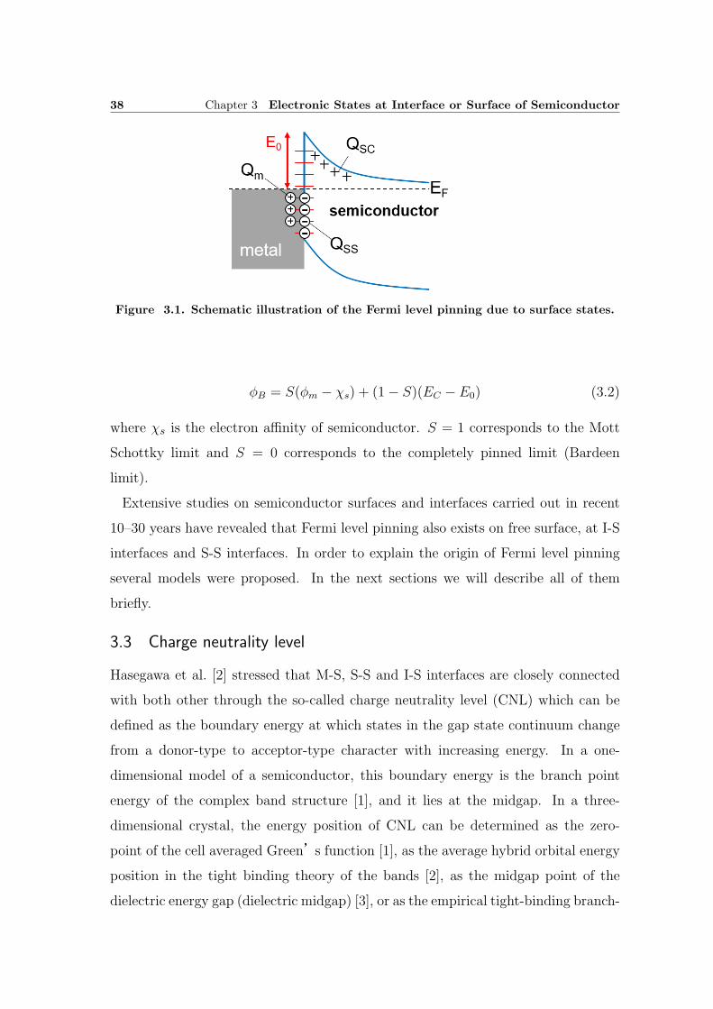
38 Chapter 3 Electronic States at Interface or Surface of Semiconductor
Figure 3.1. Schematic illustration of the Fermi level pinning due to surface states.
ϕB = S(ϕm − χs) + (1− S)(EC − E0) (3.2)
where χs is the electron affinity of semiconductor. S = 1 corresponds to the Mott
Schottky limit and S = 0 corresponds to the completely pinned limit (Bardeen
limit).
Extensive studies on semiconductor surfaces and interfaces carried out in recent
10–30 years have revealed that Fermi level pinning also exists on free surface, at I-S
interfaces and S-S interfaces. In order to explain the origin of Fermi level pinning
several models were proposed. In the next sections we will describe all of them
briefly.
3.3 Charge neutrality level
Hasegawa et al. [2] stressed that M-S, S-S and I-S interfaces are closely connected
with both other through the so-called charge neutrality level (CNL) which can be
defined as the boundary energy at which states in the gap state continuum change
from a donor-type to acceptor-type character with increasing energy. In a one-
dimensional model of a semiconductor, this boundary energy is the branch point
energy of the complex band structure [1], and it lies at the midgap. In a three-
dimensional crystal, the energy position of CNL can be determined as the zero-
point of the cell averaged Green’s function [1], as the average hybrid orbital energy
position in the tight binding theory of the bands [2], as the midgap point of the
dielectric energy gap (dielectric midgap) [3], or as the empirical tight-binding branch-
3.4 Metal-induced gap state model (MIGS) 39
point energy [4].
The roles of the CNL at the interface are the following: (1) the reference energy
for band line-up at the S-S interface (2) the Fermi level pinning point at the M-
S interface in the Bardeen limit, and (3) the Fermi level pinning point at the I-
S interface. Thus, it is an energy reference point of fundamental importance for
interfaces. .
3.4 Metal-induced gap state model (MIGS)
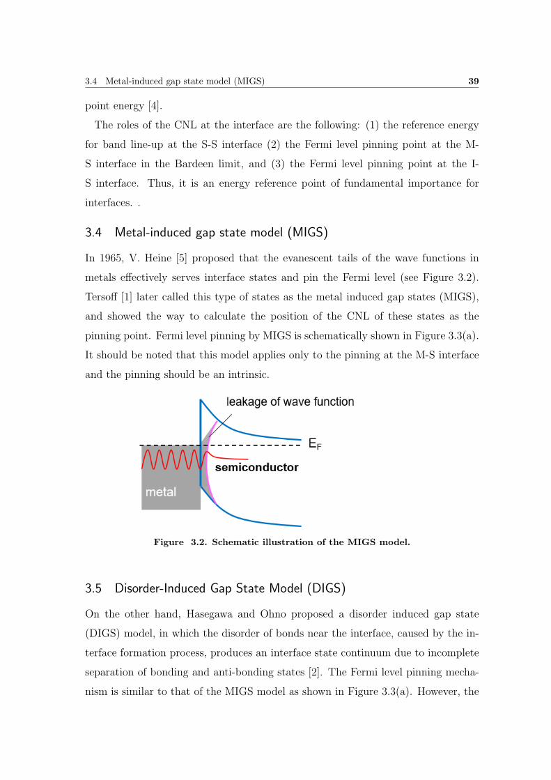
In 1965, V. Heine [5] proposed that the evanescent tails of the wave functions in
metals effectively serves interface states and pin the Fermi level (see Figure 3.2).
Tersoff [1] later called this type of states as the metal induced gap states (MIGS),
and showed the way to calculate the position of the CNL of these states as the
pinning point. Fermi level pinning by MIGS is schematically shown in Figure 3.3(a).
It should be noted that this model applies only to the pinning at the M-S interface
and the pinning should be an intrinsic.
Figure 3.2. Schematic illustration of the MIGS model.
3.5 Disorder-Induced Gap State Model (DIGS)
On the other hand, Hasegawa and Ohno proposed a disorder induced gap state
(DIGS) model, in which the disorder of bonds near the interface, caused by the in-
terface formation process, produces an interface state continuum due to incomplete
separation of bonding and anti-bonding states [2]. The Fermi level pinning mecha-
nism is similar to that of the MIGS model as shown in Figure 3.3(a). However, the
40 Chapter 3 Electronic States at Interface or Surface of Semiconductor
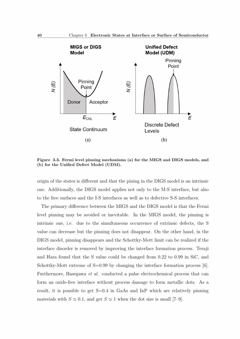
Figure 3.3. Fermi level pinning mechanisms (a) for the MIGS and DIGS models, and(b) for the Unified Defect Model (UDM).
origin of the states is different and that the pining in the DIGS model is an intrinsic
one. Additionally, the DIGS model applies not only to the M-S interface, but also
to the free surfaces and the I-S interfaces as well as to defective S-S interfaces.
The primary difference between the MIGS and the DIGS model is that the Fermi
level pinning may be avoided or inevitable. In the MIGS model, the pinning is
intrinsic one, i.e. due to the simultaneous occurrence of extrinsic defects, the S
value can decrease but the pinning does not disappear. On the other hand, in the
DIGS model, pinning disappears and the Schottky-Mott limit can be realized if the
interface disorder is removed by improving the interface formation process. Teraji
and Hara found that the S value could be changed from 0.22 to 0.99 in SiC, and
Schottky-Mott extreme of S=0.99 by changing the interface formation process [6].
Furthermore, Hasegawa et al. conducted a pulse electrochemical process that can
form an oxide-free interface without process damage to form metallic dots. As a
result, it is possible to get S=0.4 in GaAs and InP which are relatively pinning
materials with S ≃ 0.1, and get S ≃ 1 when the dot size is small [7–9].
3.6 Unified defect model (UDM) 41
3.6 Unified defect model (UDM)
As another model of extrinsic pinning, Spicer et al. [10] proposed a unified defect
model (UDM) in which near-interface discreet levels on the semiconductor side due
to processing induced native defects serve as the pinning states as shown in Figure
3.3(b). The UDM model applies not only to the M-S interface but also to the free
surface and I-S interface. The UDM model is a persuasive model but it dose not
give the experimentally observed pinning positions.
3.7 Influence of interface states at the insulator/GaN interface on the
capacitance-voltage behavior of insulator/GaN MOS structures
As was mentioned before, interface states at the I-S interface has serious implications
for the performance of GaN based devices. Therefore in the following chapters,
we will discuss the influence of the interface states on the GaN MIS structure.
Furthermore, we demonstrate a novel method for the control of the interface state
densities which was developed in our group in 2017.
3.7.1 Theoretical approach for the simulation of the GaN based MOS C-V character-
istics
In this chapter, we introduced the theoretical framework for the modeling of the
GaN based MOS C-V characteristics.
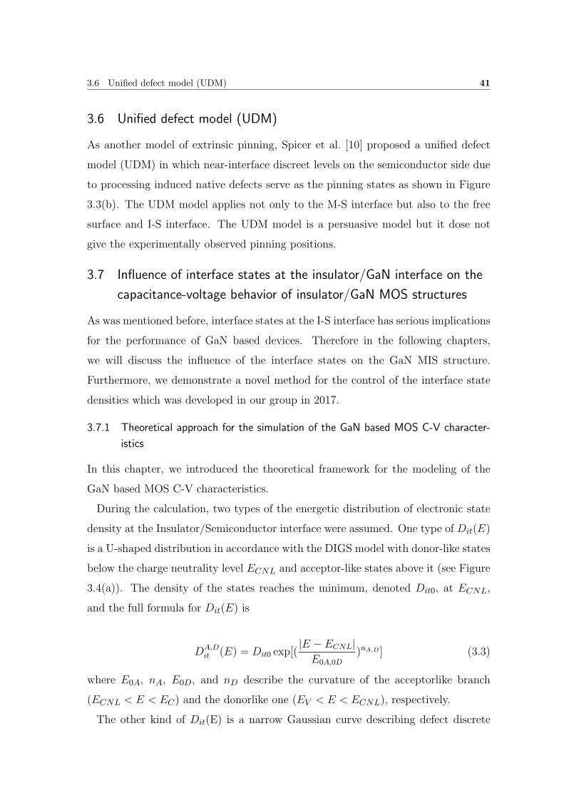
During the calculation, two types of the energetic distribution of electronic state
density at the Insulator/Semiconductor interface were assumed. One type of Dit(E)
is a U-shaped distribution in accordance with the DIGS model with donor-like states
below the charge neutrality level ECNL and acceptor-like states above it (see Figure
3.4(a)). The density of the states reaches the minimum, denoted Dit0, at ECNL,
and the full formula for Dit(E) is
DA,Dit (E) = Dit0 exp[(
|E − ECNL|E0A,0D
)nA,D ] (3.3)
where E0A, nA, E0D, and nD describe the curvature of the acceptorlike branch
(ECNL < E < EC) and the donorlike one (EV < E < ECNL), respectively.
The other kind of Dit(E) is a narrow Gaussian curve describing defect discrete
42 Chapter 3 Electronic States at Interface or Surface of Semiconductor
states (see Figure 3.4(b)),
DA,Dit Discrete(E) = Dit max exp[−4 log 2(
E − EA,D
FWHM)2] (3.4)
where Dit max is the maximum density, EA,D is the energetic location of the level,
and FWHM is the full width at half maximum of the Gaussian curve. In GaN, the
donorlike discrete state at ED = EC - 0.37 eV, which is probably related to the
N-vacancy defect [11,12], and the acceptorlike state at EA = EV + 1.0 eV, which is
related to the Ga vacancy [13,14].
Figure 3.4. Schematic illustration of (a) continuous and (b) discrete level of interfacestates.
Under the assumption that all interface states are in the thermal equilibrium with
the semiconductor, the charge in the interface traps is determined by the Fermi-Dirac
distribution f(E):
f(E) =1
1 + exp(E−EC
kT)
(3.5)
where k is the Boltzmann constant, T is temperature, and EC is the conduction
band minimum.
The occupied acceptor-like states produce negative charges, and unoccupied
donor-like states produce positive charges. The charge in the interface traps can be
expressed using the following formula:
Qit = q
∫ EC
EV
DDit (E)[1− f(E)]dE − q
∫ EC
EV
DAit(E)f(E)dE, (3.6)
where q is the elementary charge, EV is the valence band maximum, DDit and DA
it
are the density of donor-like and acceptor-like states.
3.7 Influence of interface states at the insulator/GaN interface on the capacitance-voltage behavior of insulator/GaNMOS structures43
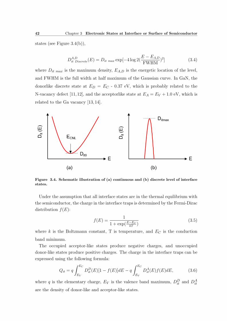
However, eq. 3.6 should be modified in order to consider the slow electron emission
from the deep interface traps [15]. Due to the wide bandgap of GaN and AlGaN, the
time constant of electron emission from the deep interface states reaches very large
values. For example, Figure 3.5 shows the calculated time constant τ as a function
of the trap energy E according to the following Shockley-Read-Hall equation:
τ =1
NCνσexp(
EC − E
kT). (3.7)
where NC , ν, and σ are the effective density of states in the conduction band, the
thermal velocity of electrons, and the capture cross section of the trap, respectively.
Figure 3.5. Time constant of electron emission from the interface traps to the con-duction band.
As can be see from Figure 3.5, for E = EC − 0.7 eV, τ is approximately equal to
100 s. On the other hand, for E = EC − 1.6 eV (midgap of GaN), τ is estimated to
be several years at room temperature. This means that only a limited number of the
interface states can be detected during the standard C-V measurements. Therefore
it is necessary to take this effect to accurately simulate C-V characteristics of GaN
based MIS structure. In this order, first we introduced the parameter ηe, which
describes efficiency emission of electrons from the trap at energy E. Based on the
SRH model, ηe can be calculated as follows:
ηe = 1− exp[−tNCνσ exp(E − EC
kT)]. (3.8)
44 Chapter 3 Electronic States at Interface or Surface of Semiconductor
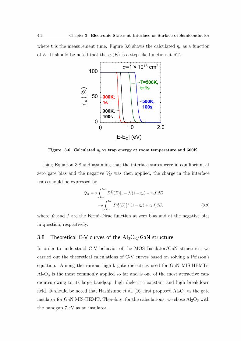
where t is the measurement time. Figure 3.6 shows the calculated ηe as a function
of E. It should be noted that the ηe(E) is a step like function at RT.
Figure 3.6. Calculated ηe vs trap energy at room temperature and 500K.
Using Equation 3.8 and assuming that the interface states were in equilibrium at
zero gate bias and the negative VG was then applied, the charge in the interface
traps should be expressed by
Qit = q
∫ EC
EV
DDit (E)[1− f0(1− ηe)− ηef ]dE
−q
∫ EC
EV
DAit(E)[f0(1− ηe) + ηef ]dE, (3.9)
where f0 and f are the Fermi-Dirac function at zero bias and at the negative bias
in question, respectively.
3.8 Theoretical C-V curves of the Al2O3/GaN structure
In order to understand C-V behavior of the MOS Insulator/GaN structures, we
carried out the theoretical calculations of C-V curves based on solving a Poisson’s
equation. Among the various high-k gate dielectrics used for GaN MIS-HEMTs,
Al2O3 is the most commonly applied so far and is one of the most attractive can-
didates owing to its large bandgap, high dielectric constant and high breakdown
field. It should be noted that Hashizume et al. [16] first proposed Al2O3 as the gate
insulator for GaN MIS-HEMT. Therefore, for the calculations, we chose Al2O3 with
the bandgap 7 eV as an insulator.
3.8 Theoretical C-V curves of the Al2O3/GaN structure 45
We assumed that in the Al2O3 layer the Poisson’s equation becomes the Laplace’s
equation:
d2V
dx2= 0. (3.10)
Furthermore, we assumed that in AlGaN and GaN layers the Poisson’s equation
takes the following form:
d2V
dx2= − q
ε0εsem(ND − n) , (3.11)
where q > 0 is the elementary charge, ε0 is the vacuum permittivity, εsem is the
relative permittivity of a semiconductor, n is the electron density and ND is the
concentration of fully ionized donor dopants.
The above equations 3.10–3.11 were solved self-consistently using the finite element
SOR method with the following boundary conditions:
• Dirichlet type boundary conditions at the contacts.
• Neumann type boundary conditions at the Al2O3/GaN interface determined
by the density of the interface state charge (Qit). In particular, the boundary
conditions at the Al2O3/GaN interface are expressed as:
ε0εsemdV
dx|sem − ε0εins
dV
dx|ins = Qit +Qfix (3.12)
where εins is the insulator (Al2O3) dielectric constant; Qit and Qfix are the sheet
density of the interface trap charge (given by Equation 3.9) and interface fixed
charge, respectively.
The solution of model equations are the in-depth distributions V (x) and n(x). The
solution was obtained for the bias VG and VG+VAC , where VAC is the amplitude of
the AC signal. On this basis, we calculated the total charge in the whole structure
for these biases, i.e., Q(VG) and Q(VG+VAC) and finally the differential capacitance
C using the following formula:
C =Q(VG)−Q(VG + VAC)
VAC
. (3.13)
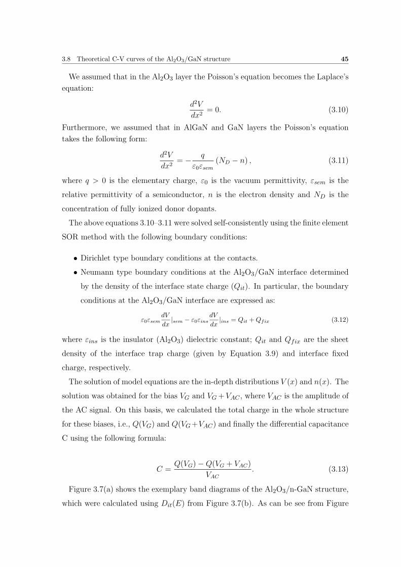
Figure 3.7(a) shows the exemplary band diagrams of the Al2O3/n-GaN structure,
which were calculated using Dit(E) from Figure 3.7(b). As can be see from Figure
46 Chapter 3 Electronic States at Interface or Surface of Semiconductor
Figure 3.7. (a)Calculated potential distribution of Al2O3/n-GaN MOS diode and(b)interface states distributions used in calculation. Etm is the deepest energy of thestate which can respond during the C-V sweeping time.
3.7(a) with the increasing Dit, the band bending increases because interface state
charge become more negative as shown in Figure 3.7(b).
3.8.1 Impact of continuous interface states on the C-V curves
In this section, we study the effect of the continuous interface states on the C-V
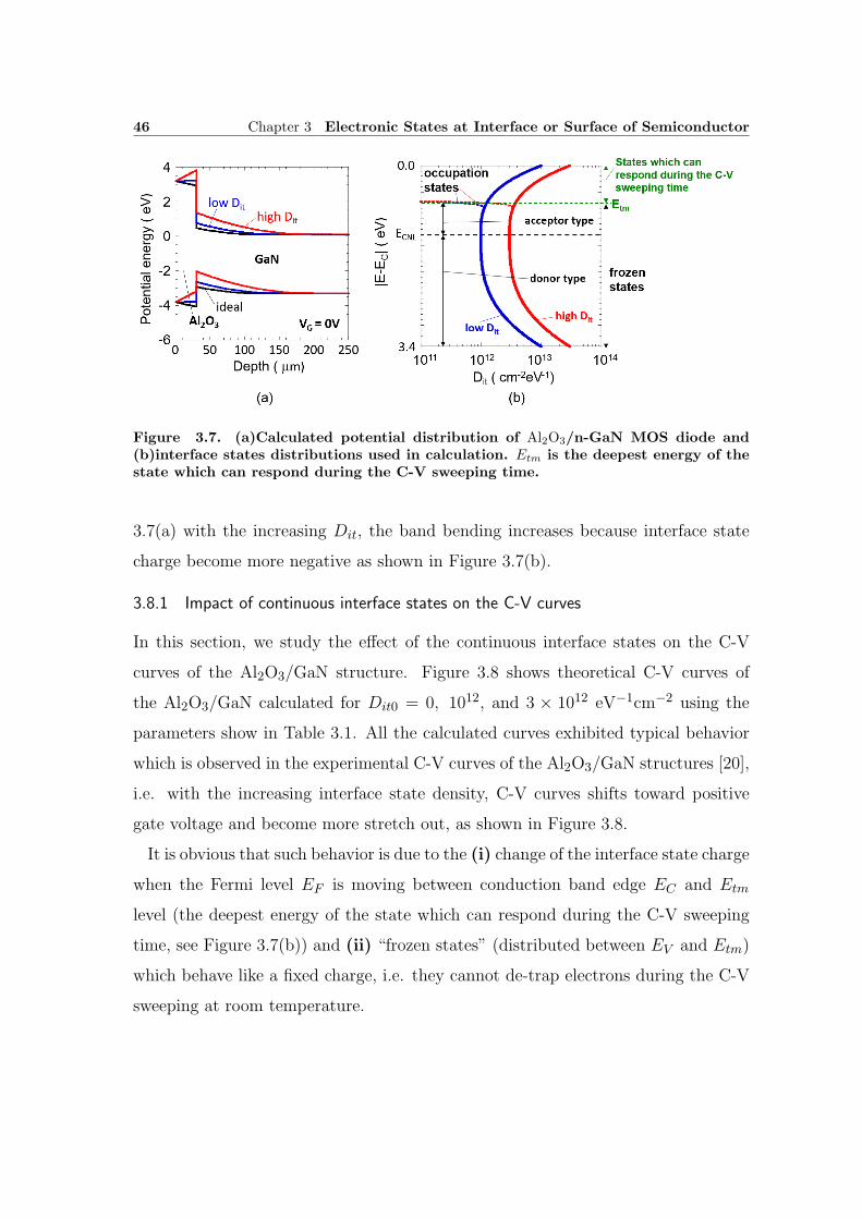
curves of the Al2O3/GaN structure. Figure 3.8 shows theoretical C-V curves of
the Al2O3/GaN calculated for Dit0 = 0, 1012, and 3 × 10¹² eV−1cm−2 using the
parameters show in Table 3.1. All the calculated curves exhibited typical behavior
which is observed in the experimental C-V curves of the Al2O3/GaN structures [20],
i.e. with the increasing interface state density, C-V curves shifts toward positive
gate voltage and become more stretch out, as shown in Figure 3.8.
It is obvious that such behavior is due to the (i) change of the interface state charge
when the Fermi level EF is moving between conduction band edge EC and Etm
level (the deepest energy of the state which can respond during the C-V sweeping
time, see Figure 3.7(b)) and (ii) “frozen states” (distributed between EV and Etm)
which behave like a fixed charge, i.e. they cannot de-trap electrons during the C-V
sweeping at room temperature.
3.8 Theoretical C-V curves of the Al2O3/GaN structure 47
Figure 3.8. Theoretical C-V curves calculated for a Al2O3/GaN MOS diode.
Table 3.1. Parameters used in the calculations. m0 is the mass of a free electron, qis the elementary charge.
Parameter name Symbol (unit) Numerical value (material or interface)Effective mass of electron me/m0 0.20 (GaN)Relative permittivity ε 9.5 (GaN)
9.0 (Al2O3)Donor concentration ND (cm−3) 5× 10¹⁶
Surface barrier height ϕs (eV) 3.4 (Ni/Al2O3) [17]Charge neutrality level ECNL EC - 1.3 eV (Al2O3/GaN) [18]Capture cross section σ (cm2) 1× 10⁻¹⁶ [19]of interface statesC-V Measurement duration t (s) 100
3.8.2 Effect of discrete interface states on the C-V curves
In this section we discuss the influence of the discrete interface states on the C-V
curves of the Al2O3/GaN structure. Figure 3.9(a) shows theoretical C-V curves of
the Al2O3/GaN structure calculated assuming the discrete level (shown in Figure
3.9(b)) and parameters from Table 3.1.
As one can see from Figure 3.9(a) acceptor-type discrete level acts like a fixed
charge at the Al2O3/GaN interface and mainly shift the C-V curve toward a more
positive voltages. On the other hand, donor-type discrete level has negligible impact
on the C-V curves. It should be noted that such behavior is quite different from
that observed in the case of the continuous interface states (see Figure 3.8). This
can be explained as follows. Namely as can be see from Figure 3.9(b) the discrete
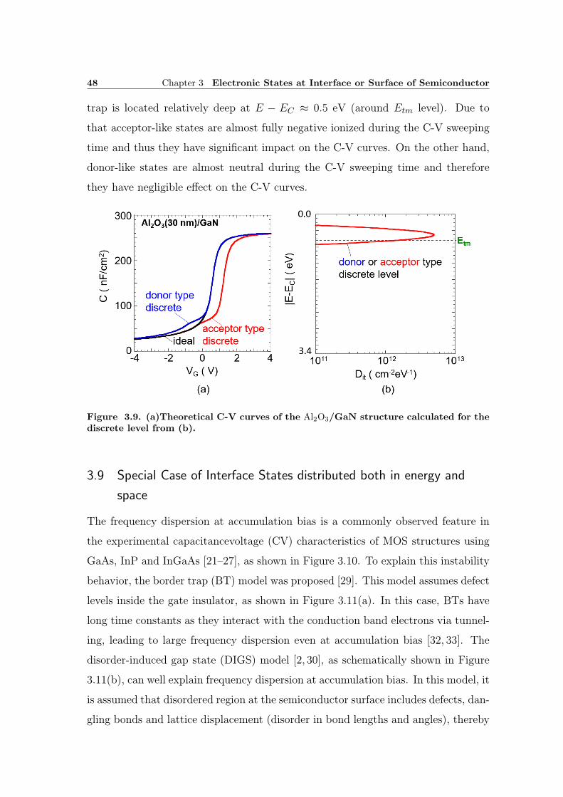
48 Chapter 3 Electronic States at Interface or Surface of Semiconductor
trap is located relatively deep at E − EC ≈ 0.5 eV (around Etm level). Due to
that acceptor-like states are almost fully negative ionized during the C-V sweeping
time and thus they have significant impact on the C-V curves. On the other hand,
donor-like states are almost neutral during the C-V sweeping time and therefore
they have negligible effect on the C-V curves.
Figure 3.9. (a)Theoretical C-V curves of the Al2O3/GaN structure calculated for thediscrete level from (b).
3.9 Special Case of Interface States distributed both in energy and
space
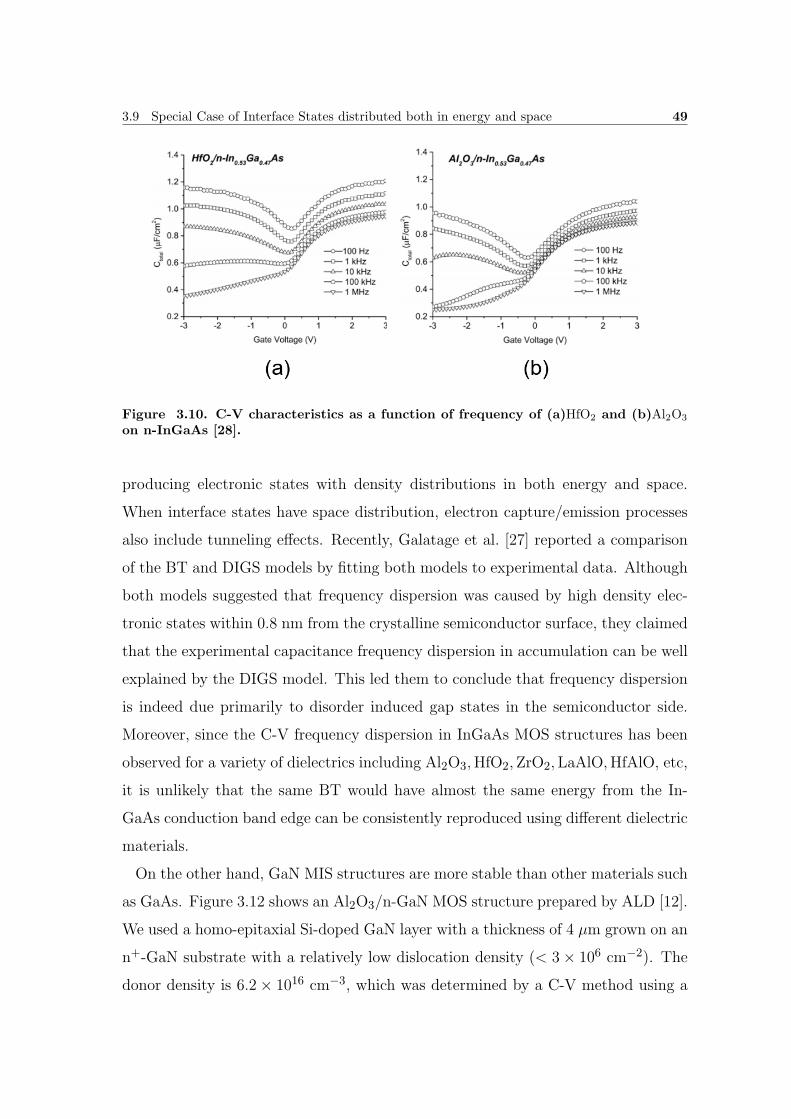
The frequency dispersion at accumulation bias is a commonly observed feature in
the experimental capacitancevoltage (CV) characteristics of MOS structures using
GaAs, InP and InGaAs [21–27], as shown in Figure 3.10. To explain this instability
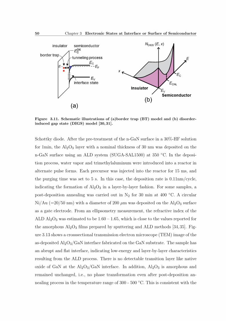
behavior, the border trap (BT) model was proposed [29]. This model assumes defect
levels inside the gate insulator, as shown in Figure 3.11(a). In this case, BTs have
long time constants as they interact with the conduction band electrons via tunnel-
ing, leading to large frequency dispersion even at accumulation bias [32, 33]. The
disorder-induced gap state (DIGS) model [2, 30], as schematically shown in Figure
3.11(b), can well explain frequency dispersion at accumulation bias. In this model, it
is assumed that disordered region at the semiconductor surface includes defects, dan-
gling bonds and lattice displacement (disorder in bond lengths and angles), thereby
3.9 Special Case of Interface States distributed both in energy and space 49
Figure 3.10. C-V characteristics as a function of frequency of (a)HfO2 and (b)Al2O3
on n-InGaAs [28].
producing electronic states with density distributions in both energy and space.
When interface states have space distribution, electron capture/emission processes
also include tunneling effects. Recently, Galatage et al. [27] reported a comparison
of the BT and DIGS models by fitting both models to experimental data. Although
both models suggested that frequency dispersion was caused by high density elec-
tronic states within 0.8 nm from the crystalline semiconductor surface, they claimed
that the experimental capacitance frequency dispersion in accumulation can be well
explained by the DIGS model. This led them to conclude that frequency dispersion
is indeed due primarily to disorder induced gap states in the semiconductor side.
Moreover, since the C-V frequency dispersion in InGaAs MOS structures has been
observed for a variety of dielectrics including Al2O3,HfO2,ZrO2,LaAlO,HfAlO, etc,
it is unlikely that the same BT would have almost the same energy from the In-
GaAs conduction band edge can be consistently reproduced using different dielectric
materials.
On the other hand, GaN MIS structures are more stable than other materials such
as GaAs. Figure 3.12 shows an Al2O3/n-GaN MOS structure prepared by ALD [12].
We used a homo-epitaxial Si-doped GaN layer with a thickness of 4 µm grown on an
n+-GaN substrate with a relatively low dislocation density (< 3× 106 cm−2). The
donor density is 6.2× 1016 cm−3, which was determined by a C-V method using a
50 Chapter 3 Electronic States at Interface or Surface of Semiconductor
Figure 3.11. Schematic illustrations of (a)border trap (BT) model and (b) disorder-induced gap state (DIGS) model [30, 31].
Schottky diode. After the pre-treatment of the n-GaN surface in a 30%-HF solution
for 1min, the Al2O3 layer with a nominal thickness of 30 nm was deposited on the
n-GaN surface using an ALD system (SUGA-SAL1500) at 350 C. In the deposi-
tion process, water vapor and trimethylaluminum were introduced into a reactor in
alternate pulse forms. Each precursor was injected into the reactor for 15 ms, and
the purging time was set to 5 s. In this case, the deposition rate is 0.11nm/cycle,
indicating the formation of Al2O3 in a layer-by-layer fashion. For some samples, a
post-deposition annealing was carried out in N2 for 30 min at 400 C. A circular
Ni/Au (=20/50 nm) with a diameter of 200 µm was deposited on the Al2O3 surface
as a gate electrode. From an ellipsometry measurement, the refractive index of the
ALD Al2O3 was estimated to be 1.60 – 1.65, which is close to the values reported for
the amorphous Al2O3 films prepared by sputtering and ALD methods [34,35]. Fig-
ure 3.13 shows a crosssectional transmission electron microscope (TEM) image of the
as-deposited Al2O3/GaN interface fabricated on the GaN substrate. The sample has
an abrupt and flat interface, indicating low-energy and layer-by-layer characteristics
resulting from the ALD process. There is no detectable transition layer like native
oxide of GaN at the Al2O3/GaN interface. In addition, Al2O3 is amorphous and
remained unchanged, i.e., no phase transformation even after post-deposition an-
nealing process in the temperature range of 300 - 500 C. This is consistent with the
3.9 Special Case of Interface States distributed both in energy and space 51
Figure 3.12. Schematic illustration of the Al2O3/n-GaN MOS structure fabricated onthe GaN substrate.
fact that the phase transformation of Al2O3 films from amorphous to crystalline hap-
pens at temperature of 800 C or higher. Figure 3.14 shows the room-temperature
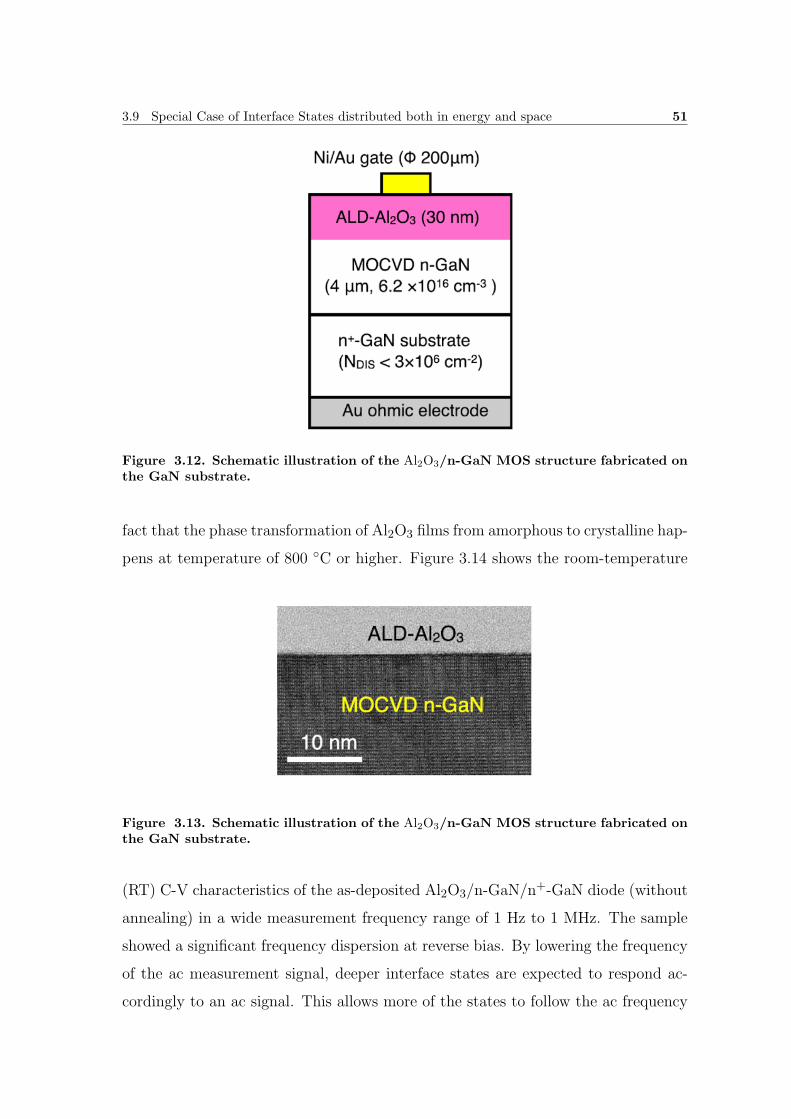
Figure 3.13. Schematic illustration of the Al2O3/n-GaN MOS structure fabricated onthe GaN substrate.
(RT) C-V characteristics of the as-deposited Al2O3/n-GaN/n+-GaN diode (without
annealing) in a wide measurement frequency range of 1 Hz to 1 MHz. The sample
showed a significant frequency dispersion at reverse bias. By lowering the frequency
of the ac measurement signal, deeper interface states are expected to respond ac-
cordingly to an ac signal. This allows more of the states to follow the ac frequency
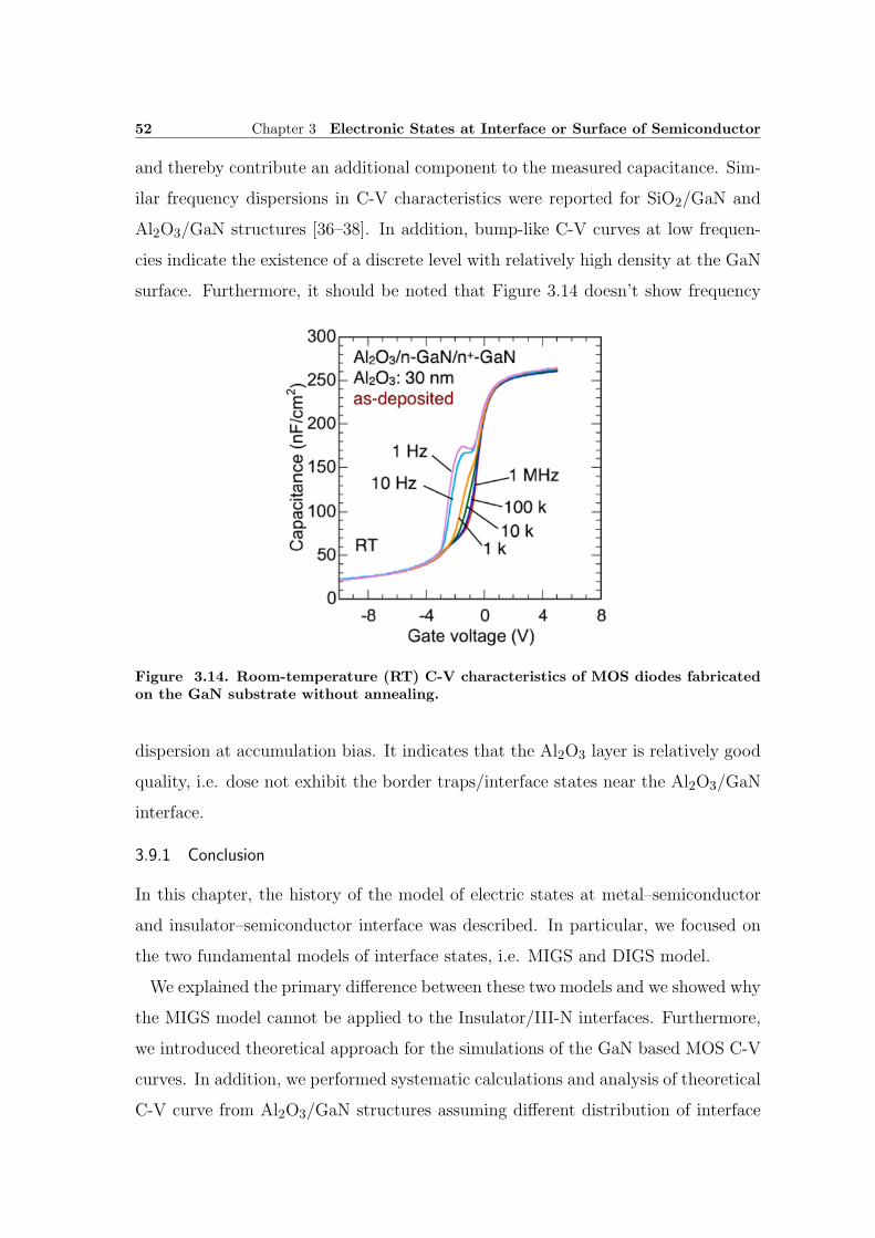
52 Chapter 3 Electronic States at Interface or Surface of Semiconductor
and thereby contribute an additional component to the measured capacitance. Sim-
ilar frequency dispersions in C-V characteristics were reported for SiO2/GaN and
Al2O3/GaN structures [36–38]. In addition, bump-like C-V curves at low frequen-
cies indicate the existence of a discrete level with relatively high density at the GaN
surface. Furthermore, it should be noted that Figure 3.14 doesn’t show frequency
Figure 3.14. Room-temperature (RT) C-V characteristics of MOS diodes fabricatedon the GaN substrate without annealing.
dispersion at accumulation bias. It indicates that the Al2O3 layer is relatively good
quality, i.e. dose not exhibit the border traps/interface states near the Al2O3/GaN
interface.
3.9.1 Conclusion
In this chapter, the history of the model of electric states at metal–semiconductor
and insulator–semiconductor interface was described. In particular, we focused on
the two fundamental models of interface states, i.e. MIGS and DIGS model.
We explained the primary difference between these two models and we showed why
the MIGS model cannot be applied to the Insulator/III-N interfaces. Furthermore,
we introduced theoretical approach for the simulations of the GaN based MOS C-V
curves. In addition, we performed systematic calculations and analysis of theoretical
C-V curve from Al2O3/GaN structures assuming different distribution of interface

3.9 Special Case of Interface States distributed both in energy and space 53
states at the Al2O3/GaN interface.

55
References
[1] J. Tersoff, Phys. Rev. Lett. 52, 465 (1984).
[2] H. Hasegawa and H. Ohno, J. Vac. Sci. Technol. B4, 1130 (1986).
[3] M. Cardona and N. E. Christensen, Phys. Rev. B 35, 6182 (1987).
[4] W. Monch, J. Appl. Phys. 80, 5076 (1996).
[5] V. Heine, Phys. Rev. 138, A1689 (1965).
[6] T. Teraji and S. Hara, Phys. Rev. B70, 035312 (2004).
[7] H. Hasegawa, T. Sato and C. Kaneshiro, J. Vac. Sci. Technol. B17, 1856 (1999).
[8] T. Sato, S. Kasai and H. Hasegawa, Appl. Surf. Sci. 175/176, 181 (2001).
[9] H. Hasegawa, T. Sato and S. Kasai, Appl. Surf. Sci. 166, 92 (2000).
[10] W. E Spicer, I. Lindau, P. R. Skeath and C. Y. Su, J. Vac. Sci. Technol. 17,
1019 (1980).
[11] E. Yamaguchi and M. R. Junnarkar, J. Cryst. Growth 189-190, 570 (1998).
[12] J. Kotani, S. Kasai, T. Hashizume, and H. Hasegawa, J. Vac. Sci. Technol. B
23, 1799 (2005).
[13] J. Neugebauer and C. G. Van de Walle, Appl. Phys. Lett. 69, 503 (1996).
[14] U. Kaufmann, M. Kunzer, H. Obloh, M. Maier, Ch. Manz, A. Ramakrishnan,
and B. Santic, Phys. Rev. B 59, 5561 (1999).
[15] W. Shockley and W. T. Read, Phys. Rev. 87, 835 (1952); R. N. Hall, ibid. 87,
387 (1952).
[16] T. Hashizume, S. Ootomo, T. Inagaki, and H. Hasegawa, J. Vac. Sci. Technol.
B 21, 1828 (2003).
[17] E. Bersch, S. Rangan, and R. A. Bartynski, Phys. Rev. B 78, 085114 (2008).
[18] W. Monch, J. Appl. Phys. 109, 113724 (2011).
[19] M. Miczek, C. Mizue, T. Hashizume, and B. Adamowicz, J. Appl. Phys. 103,
104510 (2008).
[20] S. Kaneki, J. Ohira, S. Toiya, Z. Yatabe, J. T. Asubar, and T. Hashizume,
56 References
Appl. Phys. Lett. 109, 162104 (2016).
[21] H. Hasegawa and T. Sawada, IEEE Trans. Electron Devices 27, 1055 (1980).
[22] C. L. Hinkle, A. M. Sonnet, M. Milojevic, F. S. Aguirre-Tostado, H. C. Kim,
J. Kim, R. M. Wallace, and E. M. Vogel, Appl. Phys. Lett. 93, 113506 (2008).
[23] R. V. Galatage, H. Dong, D. M. Zhernokletov, B. Brennan, C. L. Hinkle, R. M.
Wallace, and E. M. Vogel, Appl. Phys. Lett. 99, 172901 (2011).
[24] Y. Xuan, Y. Q. Wu, H. C. Lin, T. Shen, and P. D. Ye, IEEE Electron Device
Lett. 28, 935 (2007).
[25] N. Goel, P. Majhi, W. Tsai, M. Warusawithana, D. G. Schlom, M. B. Santos,
J. S. Harris, and Y. Nishi, Appl. Phys. Lett. 91, 093509 (2007).
[26] S. Koveshnikov, N. Goel, P. Majhi, H. Wen, M. B. Santos, S. Oktyabrsky, V.
Tokranov, R. Kambhampati, R. Moore, F. Zhu, J. Lee, and W. Tsai, Appl.
Phys. Lett. 92, 222904 (2008).
[27] R. V. Galatage, D. M. Zhernokletov, H. Dong, B. Brennan, C. L. Hinkle, R. M.
Wallace, and E. M. Vogel, J. Appl. Phys. 116, 014504 (2014).
[28] G. Jiao, C. Yao, Y. Xuan, D. Huang, P. D. Ye, and M.-F. Li, IEEE Trans.
Electron Devices 59, 1661 (2012).
[29] Y. Yuan, L. Wang, B. Yu, B. Shin, J. Ahn, P. C. McIntyre, P. M. Asbeck, M.
J. W. Rodwell, and Y. Taur, IEEE Electron Device Lett. 32, 485 (2011).
[30] L. He, H. Hasegawa, T. Sawada, and H. Ohno, J. Appl. Phys. 63, 2120 (1988).
[31] Z. Yatabe, J. T. Asubar, and T. Hashizume, J. Appl. D 49, 393001 (2016).
[32] H.-P. Chen, Y. Yuan, B. Yu, J. Ahn, P. C. McIntyre, P. M. Asbeck, M. J. W.
Rodwell, and Y. Taur, IEEE Trans. Electron Devices 59, 2383 (2012).
[33] G. Brammertz, A. Alian, D. H.-C. Lin, M. Meuris, M. Caymax, and W.-E.
Wang, IEEE Trans. Electron. Devices 58, 3890 (2011).
[34] Y. Jin, K. Saito, M. Shimada, and T. Ono, J. Vac. Sci. Technol., B 21, 942
(2003).
[35] S. K. Kim, S. W. Lee, C. S. Hwang, Y. S. Min, J. Y. Won, and J. Jeong, J.
Electrochem. Soc. 153, F69 (2006).
[36] B. Gaffey, L. J. Guido, X. W. Wang, and T. P. Ma, IEEE Trans. Electron
Devices 48, 458 (2001).
57
[37] K. Matocha, R. J. Gutmann, and T. P. Chow, IEEE Trans. Electron Devices
50, 1200 (2003).
[38] R. D. Long, A. Hazeghi, M. Gunji, Y. Nishi, and P. C. McIntyre, Appl. Phys.
Lett. 101, 241606 (2012).

59
Chapter 4
Evaluation of surface charging at
AlGaN surface using a dual-gate
structure
4.1 Background
In “Introduction”, the background of this chapter was described. However, in this
chapter, the background is rewritten more precisely.
There are several remaining stability issues impeding the widespread deployment
of GaN-based devices. One of the major concern is the current collapse phenomenon
which is the temporary reduction of drain current following the application of high
voltage and/or high power at both on- and off-state operations [1, 2]. According to
the most widely accepted“virtual gate”model proposed by Vetury et al. [2], cur-
rent collapse is mainly due to surface charging at a portion of the gate-drain (G-D)
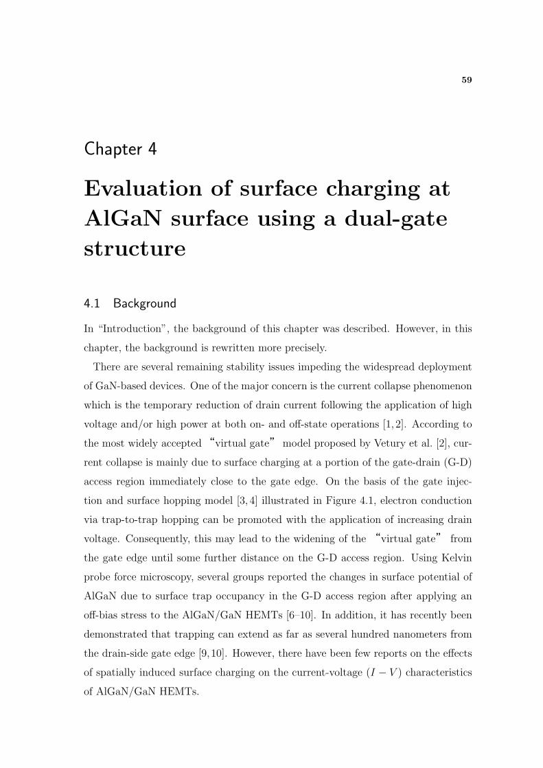
access region immediately close to the gate edge. On the basis of the gate injec-
tion and surface hopping model [3, 4] illustrated in Figure 4.1, electron conduction
via trap-to-trap hopping can be promoted with the application of increasing drain
voltage. Consequently, this may lead to the widening of the “virtual gate” from
the gate edge until some further distance on the G-D access region. Using Kelvin
probe force microscopy, several groups reported the changes in surface potential of
AlGaN due to surface trap occupancy in the G-D access region after applying an
off-bias stress to the AlGaN/GaN HEMTs [6–10]. In addition, it has recently been
demonstrated that trapping can extend as far as several hundred nanometers from
the drain-side gate edge [9,10]. However, there have been few reports on the effects
of spatially induced surface charging on the current-voltage (I − V ) characteristics
of AlGaN/GaN HEMTs.
60Chapter 4 Evaluation of surface charging at AlGaN surface using a dual-gate structure
Figure 4.1. Gate injection and surface hopping model [5].
Accordingly in one of our previous works [11], we investigated the effect of local
bias stress on access regions of AlGaN/GaN HEMTs using a dual-gate structure. In
this present communication, using the similar dual-gate architecture, we extend our
investigation to the effect of pulsed bias stress on the I − V characteristics under
which power devices in power inverter circuits are normally subjected to. The dual-
gate structure enables us to characterize the effects on the I − V characteristics
of AlGaN/GaN HEMTs of spatially induced surface charging on the access region
from the gate edges to the drain and source electrodes. We also probe the possibility
that surface charging immediately adjacent to the gate may also lead to threshold
voltage (VTH) shift.
4.2 Device structure and fabrication process
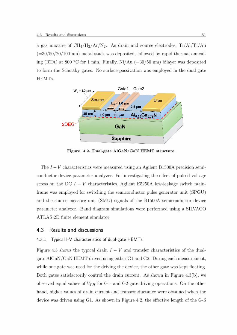
Figure 4.2 shows a schematic illustration of a dual-gate AlGaN/GaN HEMT used
in this study. The gate length (LG) and width (WG) are 1.0 and 60 µm, respec-
tively. The G1-G2 inter-gate distance is 0.5 µm. We used an Al0.25Ga0.75N/GaN
heterostructure grown on a sapphire substrate by metal-organic chemical vapor de-
position. The thicknesses of GaN and AlGaN layers are 2 µm and 25 nm, re-
spectively. Typical values of the carrier concentration and the sheet resistance are
9.0× 1012cm−2 and 470 Ω/sq, respectively. The device isolation was carried out by
reactive ion-beam etching assisted with electron-cyclotron-resonance plasma using
4.3 Results and discussions 61
a gas mixture of CH4/H2/Ar/N2. As drain and source electrodes, Ti/Al/Ti/Au
(=30/50/20/100 nm) metal stack was deposited, followed by rapid thermal anneal-
ing (RTA) at 800 C for 1 min. Finally, Ni/Au (=30/50 nm) bilayer was deposited
to form the Schottky gates. No surface passivation was employed in the dual-gate
HEMTs.
Figure 4.2. Dual-gate AlGaN/GaN HEMT structure.
The I−V characteristics were measured using an Agilent B1500A precision semi-
conductor device parameter analyzer. For investigating the effect of pulsed voltage
stress on the DC I − V characteristics, Agilent E5250A low-leakage switch main-
frame was employed for switching the semiconductor pulse generator unit (SPGU)
and the source measure unit (SMU) signals of the B1500A semiconductor device
parameter analyzer. Band diagram simulations were performed using a SILVACO
ATLAS 2D finite element simulator.
4.3 Results and discussions
4.3.1 Typical I-V characteristics of dual-gate HEMTs
Figure 4.3 shows the typical drain I − V and transfer characteristics of the dual-
gate AlGaN/GaN HEMT driven using either G1 and G2. During each measurement,
while one gate was used for the driving the device, the other gate was kept floating.
Both gates satisfactorily control the drain current. As shown in Figure 4.3(b), we
observed equal values of VTH for G1- and G2-gate driving operations. On the other
hand, higher values of drain current and transconductance were obtained when the
device was driven using G1. As shown in Figure 4.2, the effective length of the G-S
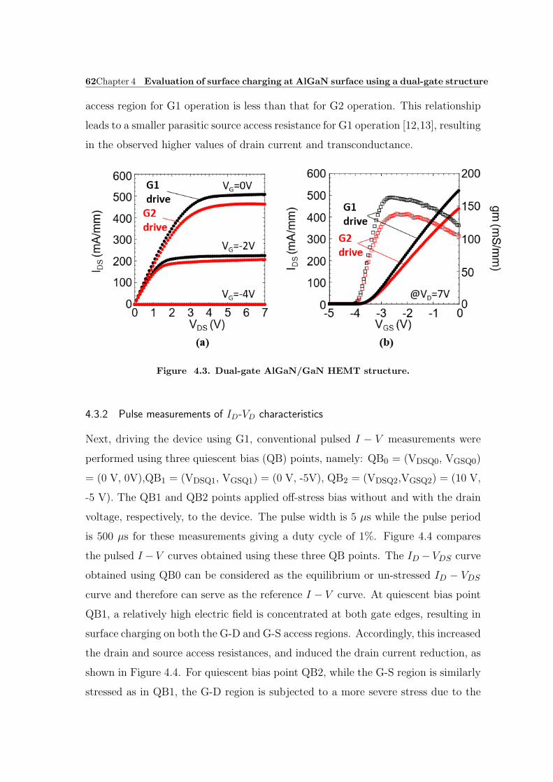
62Chapter 4 Evaluation of surface charging at AlGaN surface using a dual-gate structure
access region for G1 operation is less than that for G2 operation. This relationship
leads to a smaller parasitic source access resistance for G1 operation [12,13], resulting
in the observed higher values of drain current and transconductance.
Figure 4.3. Dual-gate AlGaN/GaN HEMT structure.
4.3.2 Pulse measurements of ID-VD characteristics
Next, driving the device using G1, conventional pulsed I − V measurements were
performed using three quiescent bias (QB) points, namely: QB0 = (VDSQ0, VGSQ0)
= (0 V, 0V),QB1 = (VDSQ1, VGSQ1) = (0 V, -5V), QB2 = (VDSQ2,VGSQ2) = (10 V,
-5 V). The QB1 and QB2 points applied off-stress bias without and with the drain
voltage, respectively, to the device. The pulse width is 5 µs while the pulse period
is 500 µs for these measurements giving a duty cycle of 1%. Figure 4.4 compares
the pulsed I − V curves obtained using these three QB points. The ID − VDS curve
obtained using QB0 can be considered as the equilibrium or un-stressed ID − VDS
curve and therefore can serve as the reference I − V curve. At quiescent bias point
QB1, a relatively high electric field is concentrated at both gate edges, resulting in
surface charging on both the G-D and G-S access regions. Accordingly, this increased
the drain and source access resistances, and induced the drain current reduction, as
shown in Figure 4.4. For quiescent bias point QB2, while the G-S region is similarly
stressed as in QB1, the G-D region is subjected to a more severe stress due to the
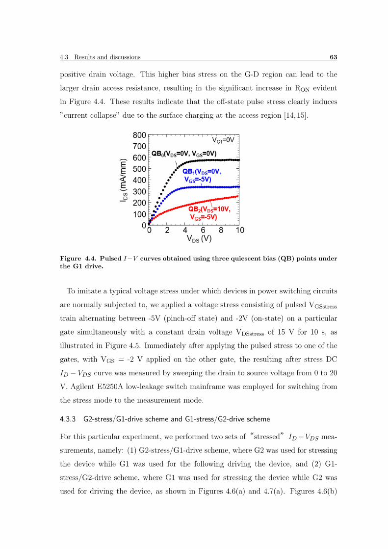
4.3 Results and discussions 63
positive drain voltage. This higher bias stress on the G-D region can lead to the
larger drain access resistance, resulting in the significant increase in RON evident
in Figure 4.4. These results indicate that the off-state pulse stress clearly induces
”current collapse” due to the surface charging at the access region [14,15].
Figure 4.4. Pulsed I−V curves obtained using three quiescent bias (QB) points underthe G1 drive.
To imitate a typical voltage stress under which devices in power switching circuits
are normally subjected to, we applied a voltage stress consisting of pulsed VGSstress
train alternating between -5V (pinch-off state) and -2V (on-state) on a particular
gate simultaneously with a constant drain voltage VDSstress of 15 V for 10 s, as
illustrated in Figure 4.5. Immediately after applying the pulsed stress to one of the
gates, with VGS = -2 V applied on the other gate, the resulting after stress DC
ID − VDS curve was measured by sweeping the drain to source voltage from 0 to 20
V. Agilent E5250A low-leakage switch mainframe was employed for switching from
the stress mode to the measurement mode.
4.3.3 G2-stress/G1-drive scheme and G1-stress/G2-drive scheme
For this particular experiment, we performed two sets of“stressed”ID−VDS mea-
surements, namely: (1) G2-stress/G1-drive scheme, where G2 was used for stressing
the device while G1 was used for the following driving the device, and (2) G1-
stress/G2-drive scheme, where G1 was used for stressing the device while G2 was
used for driving the device, as shown in Figures 4.6(a) and 4.7(a). Figures 4.6(b)
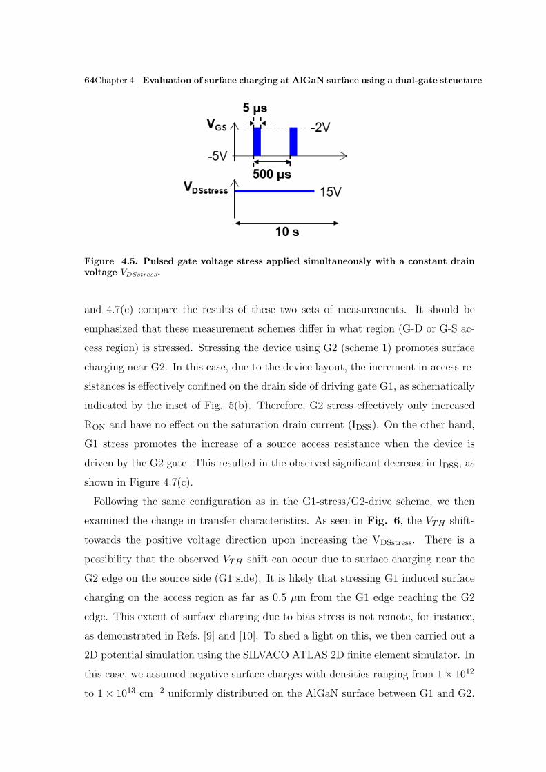
64Chapter 4 Evaluation of surface charging at AlGaN surface using a dual-gate structure
Figure 4.5. Pulsed gate voltage stress applied simultaneously with a constant drainvoltage VDSstress.
and 4.7(c) compare the results of these two sets of measurements. It should be
emphasized that these measurement schemes differ in what region (G-D or G-S ac-
cess region) is stressed. Stressing the device using G2 (scheme 1) promotes surface
charging near G2. In this case, due to the device layout, the increment in access re-
sistances is effectively confined on the drain side of driving gate G1, as schematically
indicated by the inset of Fig. 5(b). Therefore, G2 stress effectively only increased
RON and have no effect on the saturation drain current (IDSS). On the other hand,
G1 stress promotes the increase of a source access resistance when the device is
driven by the G2 gate. This resulted in the observed significant decrease in IDSS, as
shown in Figure 4.7(c).
Following the same configuration as in the G1-stress/G2-drive scheme, we then
examined the change in transfer characteristics. As seen in Fig. 6, the VTH shifts
towards the positive voltage direction upon increasing the VDSstress. There is a
possibility that the observed VTH shift can occur due to surface charging near the
G2 edge on the source side (G1 side). It is likely that stressing G1 induced surface
charging on the access region as far as 0.5 µm from the G1 edge reaching the G2
edge. This extent of surface charging due to bias stress is not remote, for instance,
as demonstrated in Refs. [9] and [10]. To shed a light on this, we then carried out a
2D potential simulation using the SILVACO ATLAS 2D finite element simulator. In
this case, we assumed negative surface charges with densities ranging from 1× 10¹²
to 1× 1013 cm−2 uniformly distributed on the AlGaN surface between G1 and G2.
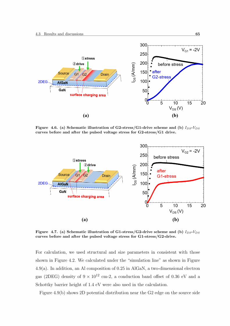
4.3 Results and discussions 65
Figure 4.6. (a) Schematic illustration of G2-stress/G1-drive scheme and (b) IDS-VDS
curves before and after the pulsed voltage stress for G2-stress/G1 drive.
Figure 4.7. (a) Schematic illustration of G1-stress/G2-drive scheme and (b) IDS-VDS
curves before and after the pulsed voltage stress for G1-stress/G2-drive.
For calculation, we used structural and size parameters in consistent with those
shown in Figure 4.2. We calculated under the “simulation line” as shown in Figure
4.9(a). In addition, an Al composition of 0.25 in AlGaN, a two-dimensional electron
gas (2DEG) density of 9 × 1012 cm-2, a conduction band offset of 0.36 eV and a
Schottky barrier height of 1.4 eV were also used in the calculation.
Figure 4.9(b) shows 2D potential distribution near the G2 edge on the source side
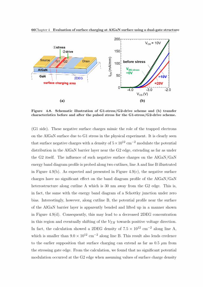
66Chapter 4 Evaluation of surface charging at AlGaN surface using a dual-gate structure
Figure 4.8. Schematic illustration of G1-stress/G2-drive scheme and (b) transfercharacteristics before and after the pulsed stress for the G1-stress/G2-drive scheme.
(G1 side). These negative surface charges mimic the role of the trapped electrons
on the AlGaN surface due to G1 stress in the physical experiment. It is clearly seen
that surface negative charges with a density of 5×1012 cm−2 modulate the potential
distribution in the AlGaN barrier layer near the G2 edge, extending as far as under
the G2 itself. The influence of such negative surface charges on the AlGaN/GaN
energy band diagram profile is probed along two cutlines, line A and line B illustrated
in Figure 4.9(b). As expected and presented in Figure 4.9(c), the negative surface
charges have no significant effect on the band diagram profile of the AlGaN/GaN
heterostructure along cutline A which is 30 nm away from the G2 edge. This is,
in fact, the same with the energy band diagram of a Schottky junction under zero
bias. Interestingly, however, along cutline B, the potential profile near the surface
of the AlGaN barrier layer is apparently bended and lifted up in a manner shown
in Figure 4.9(d). Consequently, this may lead to a decreased 2DEG concentration
in this region and eventually shifting of the VTH towards positive voltage direction.
In fact, the calculation showed a 2DEG density of 7.5 × 1012 cm−2 along line A,
which is smaller than 9.0× 1012 cm−2 along line B. This result also lends credence
to the earlier supposition that surface charging can extend as far as 0.5 µm from
the stressing gate edge. From the calculation, we found that no significant potential
modulation occurred at the G2 edge when assuming values of surface charge density
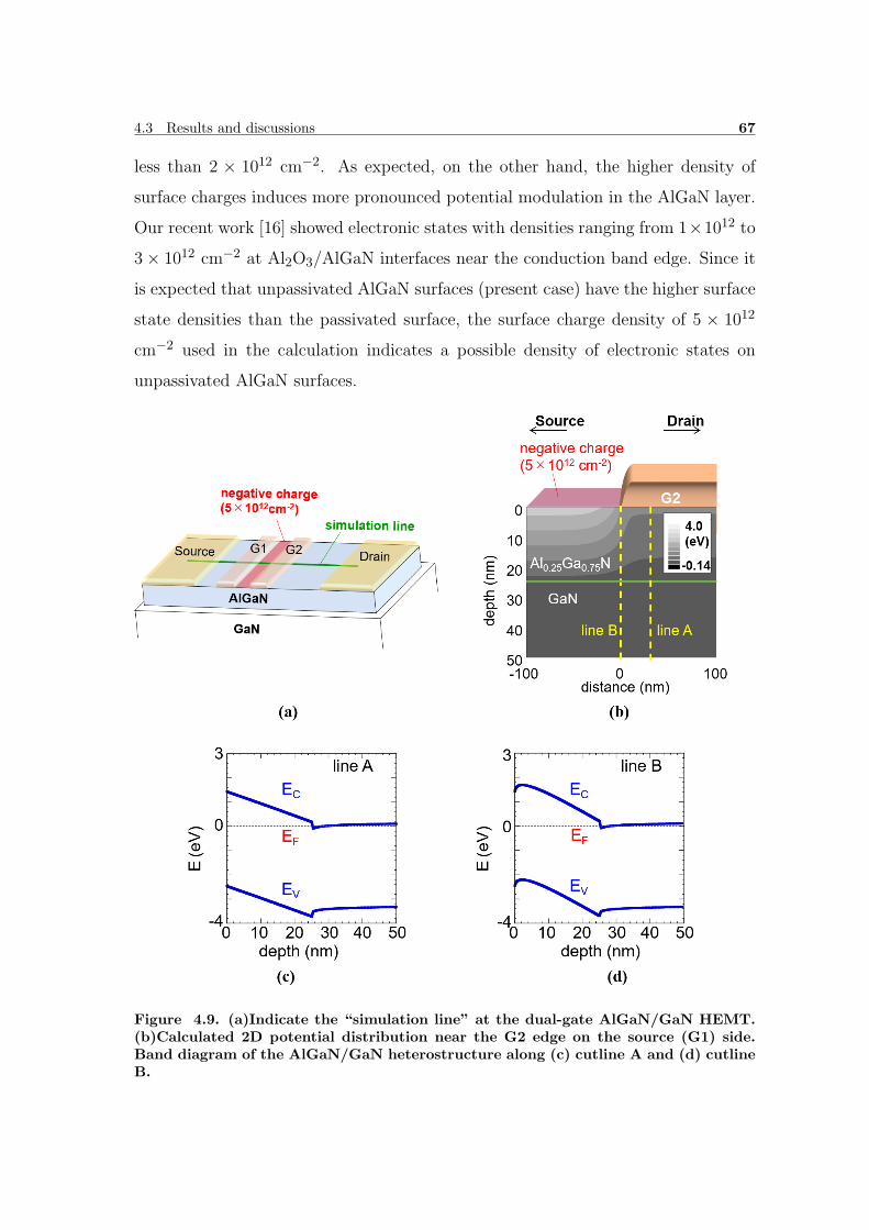
4.3 Results and discussions 67
less than 2 × 1012 cm−2. As expected, on the other hand, the higher density of
surface charges induces more pronounced potential modulation in the AlGaN layer.
Our recent work [16] showed electronic states with densities ranging from 1×10¹² to
3× 1012 cm−2 at Al2O3/AlGaN interfaces near the conduction band edge. Since it
is expected that unpassivated AlGaN surfaces (present case) have the higher surface
state densities than the passivated surface, the surface charge density of 5 × 10¹²
cm−2 used in the calculation indicates a possible density of electronic states on
unpassivated AlGaN surfaces.
Figure 4.9. (a)Indicate the “simulation line” at the dual-gate AlGaN/GaN HEMT.(b)Calculated 2D potential distribution near the G2 edge on the source (G1) side.Band diagram of the AlGaN/GaN heterostructure along (c) cutline A and (d) cutlineB.
68Chapter 4 Evaluation of surface charging at AlGaN surface using a dual-gate structure
In the G2-stress/G1-drive scheme corresponding to the IDS−VDS curves in Figure
4.6(b), on the other hand, no VTH shift was observed. The electric field on the gate
edge of the source side is much lower than that on the drain side. Thus stressing G2
induced a weak extension of surface charging on the source side, as schematically
shown in Figure 4.6(a). Therefore, the surface charging region is sufficiently far from
the G1 edges, leading to no VTH shift during G1 drive operation after the G2 stress.
The calculation indicates that no significant potential modulation occurs when the
surface charging region is 50 nm far from the gate edge, even though the surface
charge density is 5× 1012 cm−2 or higher.
4.4 Conclusion
In summary, we have evaluated off-bias-stress spatially induced surface charging
effects using a dual-gate HEMT structure. Pulsed voltage stress on the G-D access
region leads only to increase in RON of the device. On the other hand, pulsed
voltage stress on the G-S region leads not only to increase in RON but also to
decrease in IDSS. In the case of the G1-stress/G2-drive operation, we observed a
clear VTH shift towards the positive voltage direction upon increasing the VDSstress.
The 2D potential simulation indicated that surface negative charges induced by the
G1 stress modulate the potential distribution in the AlGaN barrier layer near the G2
edge where the potential near the surface of the AlGaN barrier layer are apparently
bended and lifted. Consequently, this may lead to a decreased 2DEG concentration
in this region and eventually shifting of the VTH towards positive voltage direction.
It was also found that such surface charging can extend as far as 0.5 µm from the
stressing gate edge. For accrual device technology, we will have to investigate effects
of a surface passivation [17] and/or a field plate structures [18,19] on surface charging
region at the AlGaN surface.
69
References
[1] M. A. Khan, M. S. Shur, Q. C. Chen, and J. N. Kuznia, Electron. Lett. 30,
2175 (1994).
[2] R. Vetury, N. Q. Zhang, S. Keller, and U. K. Mishra, IEEE Trans. Electron
Devices 48, 560 (2001).
[3] R. J. Trew, D. S. Green, and J. B. Shealy, IEEE Microwave Mag. 10 [4], 116
(2009).
[4] J. Kotani, M. Tajima, S. Kasai, and T. Hashizume, Appl. Phys. Lett. 91, 093501
(2007).
[5] U. K. Mishra, L. Shen, T. E. Kazior, and Y.-F. Wu, Proc. IEEE 96, 287 (2008).
[6] G. Koley, V. Tilak, L. F. Eastman, and M. G. Spencer, IEEE Trans. Electron
Devices 50, 886 (2003).
[7] K. Nakagami, Y. Ohno, S. Kishimoto, K. Maezawa, and T. Mizutani, Appl.
Phys. Lett. 85, 6028 (2004).
[8] S. Kamiya, M. Iwami, T. Tsuchiya, M. Kurouchi, J. Kikawa, T. Yamada, A.
Wakejima, H. Miyamoto, A. Suzuki, A. Hinoki, T. Araki, and Y. Nanishi, Appl.
Phys. Lett. 90, 213511 (2007).
[9] S. DasGupta, L. B. Biedermann, M. Sun, R. Kaplar, M. Marinella, K. R.
Zavadil, S. Atcitty, and T. Palacios, Appl. Phys. Lett. 101, 243506 (2012).
[10] D. W. Cardwell, A. R. Arehart, C. Poblenz, Y. Pei, J. S. Speck, U. K. Mishra,
S. A. Ringel, and J. P. Pelz, Appl. Phys. Lett. 100, 193507 (2012).
[11] M. Tajima and T. Hashizume, Jpn. J. Appl. Phys. 50, 061001 (2011).
[12] S. Russo and A. D. Carlo, IEEE Trans. Electron Devices 54, 1071 (2007).
[13] C. Y. Lu, E. B. Treidel, O. Hilt, R. Lossy, N. Chaturvedi, E. Y. Chang, J.
Wurfl, and G. Trankle, Semicond. Sci. Technol. 25, 075005 (2010).
[14] G. Meneghesso, F. Rampazzo, P. Kordos, G. Verzellesi, and E. Zanoni, IEEE
Trans. Electron Devices 53, 2932 (2006).
70 References
[15] G. Meneghesso, G. Verzellesi, F. Danesin, F. Rampazzo, F. Zanon, A. Tazzoli,
M. Meneghini, and E. Zanoni, IEEE Trans. Device Mater. Reliab. 8, 332 (2008).
[16] C. Mizue, Y. Hori, M. Miczek, and T. Hashizume, Jpn. J. Appl. Phys. 50,
021001 (2011).
[17] T. Hashizume, S. Ootomo, T. Inagaki, and H. Hasegawa, J. Vac. Sci. Technol.
B 21, 1828 (2003).
[18] S. Karmalkar and U. K. Mishra, IEEE Trans. Electron Devices 48, 1515 (2001).
[19] Y. Ando, Y. Okamoto, H. Miyamoto, T. Nakayama, T. Inoue, and M. Kuzuhara,
IEEE Electron Device Lett. 24, 289 (2003).
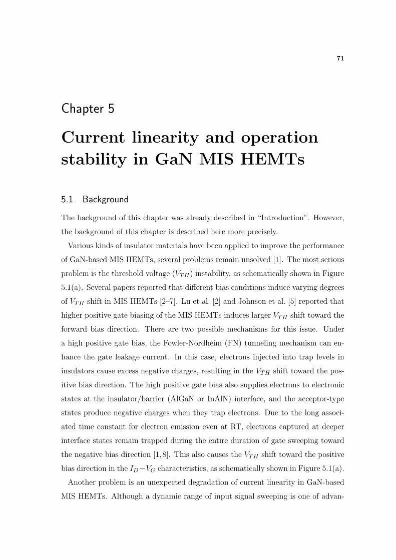
71
Chapter 5
Current linearity and operation
stability in GaN MIS HEMTs
5.1 Background
The background of this chapter was already described in “Introduction”. However,
the background of this chapter is described here more precisely.
Various kinds of insulator materials have been applied to improve the performance
of GaN-based MIS HEMTs, several problems remain unsolved [1]. The most serious
problem is the threshold voltage (VTH) instability, as schematically shown in Figure
5.1(a). Several papers reported that different bias conditions induce varying degrees
of VTH shift in MIS HEMTs [2–7]. Lu et al. [2] and Johnson et al. [5] reported that
higher positive gate biasing of the MIS HEMTs induces larger VTH shift toward the
forward bias direction. There are two possible mechanisms for this issue. Under
a high positive gate bias, the Fowler-Nordheim (FN) tunneling mechanism can en-
hance the gate leakage current. In this case, electrons injected into trap levels in
insulators cause excess negative charges, resulting in the VTH shift toward the pos-
itive bias direction. The high positive gate bias also supplies electrons to electronic
states at the insulator/barrier (AlGaN or InAlN) interface, and the acceptor-type
states produce negative charges when they trap electrons. Due to the long associ-
ated time constant for electron emission even at RT, electrons captured at deeper
interface states remain trapped during the entire duration of gate sweeping toward
the negative bias direction [1,8]. This also causes the VTH shift toward the positive
bias direction in the ID−VG characteristics, as schematically shown in Figure 5.1(a).
Another problem is an unexpected degradation of current linearity in GaN-based
MIS HEMTs. Although a dynamic range of input signal sweeping is one of advan-
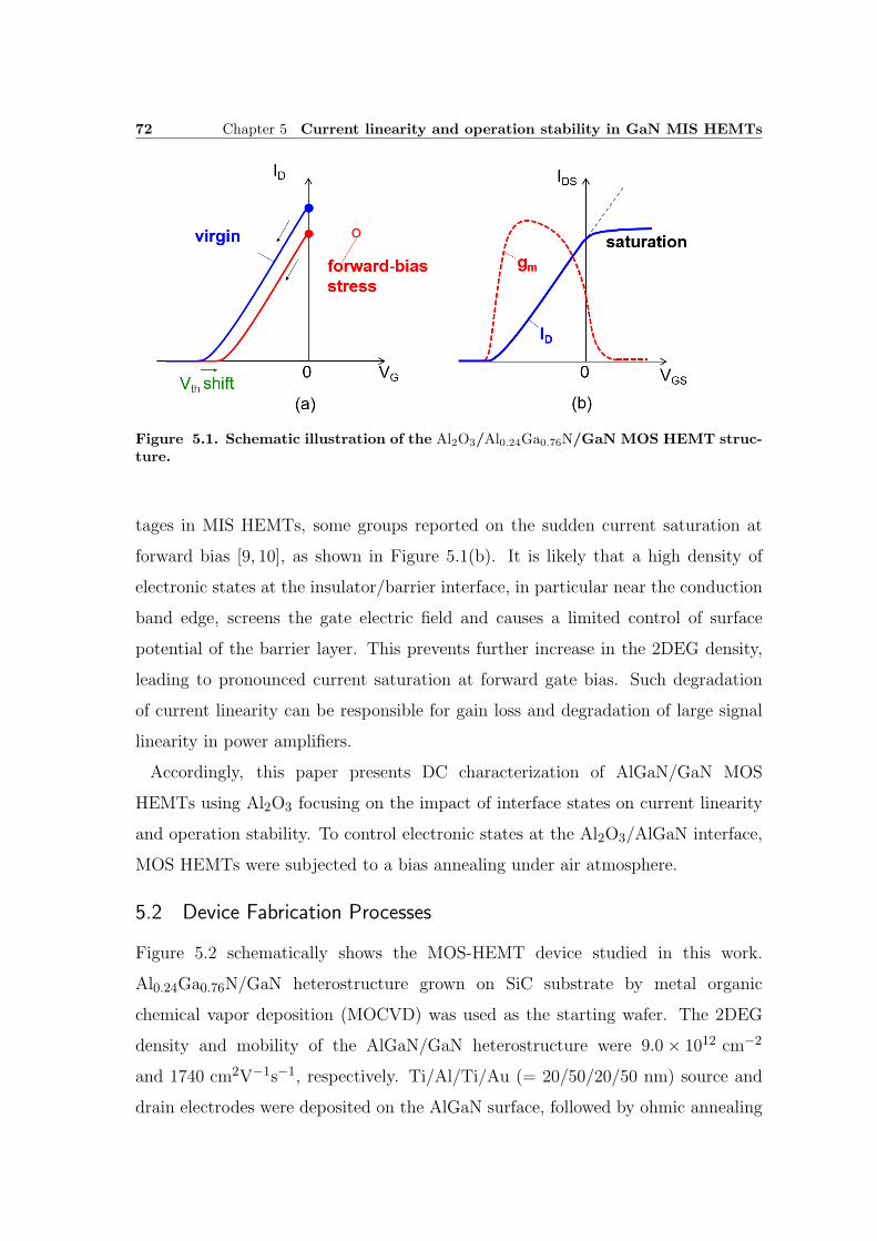
72 Chapter 5 Current linearity and operation stability in GaN MIS HEMTs
Figure 5.1. Schematic illustration of the Al2O3/Al0.24Ga0.76N/GaN MOS HEMT struc-ture.
tages in MIS HEMTs, some groups reported on the sudden current saturation at
forward bias [9, 10], as shown in Figure 5.1(b). It is likely that a high density of
electronic states at the insulator/barrier interface, in particular near the conduction
band edge, screens the gate electric field and causes a limited control of surface
potential of the barrier layer. This prevents further increase in the 2DEG density,
leading to pronounced current saturation at forward gate bias. Such degradation
of current linearity can be responsible for gain loss and degradation of large signal
linearity in power amplifiers.
Accordingly, this paper presents DC characterization of AlGaN/GaN MOS
HEMTs using Al2O3 focusing on the impact of interface states on current linearity
and operation stability. To control electronic states at the Al2O3/AlGaN interface,
MOS HEMTs were subjected to a bias annealing under air atmosphere.
5.2 Device Fabrication Processes
Figure 5.2 schematically shows the MOS-HEMT device studied in this work.
Al0.24Ga0.76N/GaN heterostructure grown on SiC substrate by metal organic
chemical vapor deposition (MOCVD) was used as the starting wafer. The 2DEG
density and mobility of the AlGaN/GaN heterostructure were 9.0× 1012 cm−2
and 1740 cm2V−1s−1, respectively. Ti/Al/Ti/Au (= 20/50/20/50 nm) source and
drain electrodes were deposited on the AlGaN surface, followed by ohmic annealing
5.3 Extremely Decreased Electronic States at Al2O3/n-GaN Interface by Reverse-Bias Annealing73
at 830 C for 1 min in N2 ambient. As a surface protection layer during ohmic
annealing, a 20-nm-thick SiN film was deposited to prevent damage to the AlGaN
surface [11]. After the ohmic metallization process, the SiN film was removed
using a buffered HF solution. An Al2O3 layer with a nominal thickness of 30 nm
was then deposited on the AlGaN surface using an atomic layer deposition (ALD)
system (SUGA-SAL1500) at 300 C. In the deposition process, water vapor and
trimethylaluminum were introduced into a reactor in alternate pulse forms. Each
precursor was injected into the reactor for 15 ms, and the purging time was set to
5 s. In this case, the deposition rate is 0.11 nm/cycle, facilitating the formation of
Al2O3 in a layer-by-layer fashion. Finally, the device fabrication was completed by
electron beam evaporation of Ni/Au bilayer and subsequent lift-off process to form
the gate electrode. The gate length, gate width, and gate-drain distance were 5,
100, and 10 µm, respectively.
Figure 5.2. Schematic illustration of the Al2O3/Al0.24Ga0.76N/GaN MOS HEMT struc-ture.
5.3 Extremely Decreased Electronic States at Al2O3/n-GaN Interface
by Reverse-Bias Annealing
The process of our group to decrease the interface state density is proposed in
this section. To improve the interface properties of GaN MIS structures, we have
carried out various kinds of control processes including post-deposition and post-

74 Chapter 5 Current linearity and operation stability in GaN MIS HEMTs
metallization annealing processes. As described in Ref. [12], Al2O3/GaN/n+-GaN
MOS diodes described in chapter 3.9 were applied a standard post-deposition an-
nealing at 400-700 C in N2 for 30 min. It was effective in decreasing state densi-
ties at the Al2O3/GaN interface. Even in this case, the interface state density of
5× 1011cm−1eV−1 or higher remained, indicating that the post-deposition annealing
is insufficient for controlling interface states.
However, we then found that the “reverse-bias annealing” in air, at 300 C, and
under reverse voltage (-10 V) is more effective in achieving excellent C-V charac-
teristics with negligible frequency dispersion , as shown in Figure 5.3(a). The C-V
Figure 5.3. (a)Room-temperature (RT) C-V characteristics of MOS diodes fabricatedon the GaN substrate with reverse-bias annealing and (b)interface state density (Dit)distributions determined by applying the Terman method to 1-MHz C-V results forAl2O3/GaN/n+-GaN.
curves of the bias-annealed sample are very close to the calculated curve (broken
line) with no such bump-like behavior in a very wide frequency range of 1 Hz - 1
MHz. There is a difference of flat-band voltage (VFB) between samples without
and with the reverse-bias annealing. Again, on the one hand, the annealed sample
exhibited a VFB very close to the calculated value; while, on the other hand, the
as-deposited sample showed a VFB shift toward the negative bias direction, probably
due to excess positive charges arising from donor-type interface states and/or defect
levels in the bulk Al2O3. As mentioned below, the bias-annealing process decreased
5.3 Extremely Decreased Electronic States at Al2O3/n-GaN Interface by Reverse-Bias Annealing75
such states and levels, resulting in the VFB recovery to the expected value.
Figure 5.3(b) shows the interface state density distributions of Al2O3/GaN in-
terfaces determined by applying the Terman method to 1 MHz CV results for the
Al2O3/n-GaN/n+-GaN structure. Note that the time constant of electron emission
is extremely long at RT for interface states with deep energies relative to the con-
duction band edge. We thus plotted the evaluated data within the range EC - 0.8
eV in Figure 5.3(b). The as-deposited sample exhibited relatively high state densi-
ties in the range of 1012 cm−2eV−1. In addition, a peak corresponding to a density
of 2× 1012 cm−2eV−1 appeared at around EC - 0.6 eV, probably arising from a
discrete trap related to the nitrogen-vacancy defects [13–15]. After post-deposition
annealing at 400 C, the interface state density was decreased. Even in this case,
however, the state densities of 5× 1011 cm−2eV−1 or higher remained. On the other
hand, the reverse-bias annealing in air at 300 C for 3 h resulted in a significant
reduction in state density. In fact, the reverse-bias-annealed sample showed a state
density below the detection limit (< 1× 1011 cm−2eV−1) except for those energies
near the conduction band edge, corresponding to nearly ideal C-V curves without
frequency dispersion as shown in Figure 5.3(a).
Figure 5.4 shows the C-V characteristics measured at 200 C for the Al2O3/n-
GaN/n+-GaN structure with the reverse-bias annealing. For high temperature C-V
measurements, it is expected that deeper interface states can respond both to bias
sweeping and ac signal modulation, causing changes in C-V characteristics compared
with those measured at RT. In fact, Matocha et al., [16,17] Ooyama et al., [18] and
Long et al. [19] reported significant stretch-out of C-V curves, bump-like C-V behav-
ior, and enhanced frequency dispersion for SiO2/GaN and Al2O3/GaN structures
at measurement temperatures from 175 to 300 C. Such unstable C-V behavior at
high temperatures indicates that relatively high-density interface states can cause
operation instability in GaN-based MOSFETs. In our reverse-bias annealed sam-
ple, however, the high-temperature C-V behavior remained almost unchanged, as
compared with the RT C-V curves shown in Figure 5.4. In particular, negligible
frequency dispersion and the same C-V slope were observed even at high tempera-
ture of 200 C. These results indicate that the present process applied on a MOS
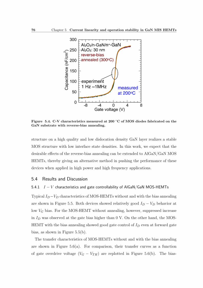
76 Chapter 5 Current linearity and operation stability in GaN MIS HEMTs
Figure 5.4. C-V characteristics measured at 200 C of MOS diodes fabricated on theGaN substrate with reverse-bias annealing.
structure on a high quality and low dislocation density GaN layer realizes a stable
MOS structure with low interface state densities. In this work, we expect that the
desirable effects of the reverse-bias annealing can be extended to AlGaN/GaN MOS
HEMTs, thereby giving an alternative method in pushing the performance of these
devices when applied in high power and high frequency applications.
5.4 Results and Discussion
5.4.1 I − V characteristics and gate controllability of AlGaN/GaN MOS-HEMTs
Typical ID−VD characteristics of MOS-HEMTs without and with the bias annealing
are shown in Figure 5.5. Both devices showed relatively good ID − VD behavior at
low VG bias. For the MOS-HEMT without annealing, however, suppressed increase
in ID was observed at the gate bias higher than 0 V. On the other hand, the MOS-
HEMT with the bias annealing showed good gate control of ID even at forward gate
bias, as shown in Figure 5.5(b).
The transfer characteristics of MOS-HEMTs without and with the bias annealing
are shown in Figure 5.6(a). For comparison, their transfer curves as a function
of gate overdrive voltage (VG − VTH) are replotted in Figure 5.6(b). The bias-
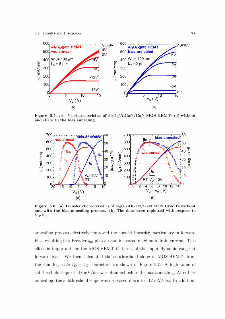
5.4 Results and Discussion 77
Figure 5.5. ID − VD characteristics of Al2O3/AlGaN/GaN MOS HEMTs (a) withoutand (b) with the bias annealing.
Figure 5.6. (a) Transfer characteristics of Al2O3/AlGaN/GaN MOS HEMTs withoutand with the bias annealing process. (b) The data were replotted with respect toVG-Vth.
annealing process effectively improved the current linearity, particulary in forward
bias, resulting in a broader gm plateau and increased maximum drain current. This
effect is important for the MOS-HEMT in terms of the input dynamic range at
forward bias. We then calculated the subthreshold slope of MOS-HEMTs from
the semi-log scale ID − VG characteristics shown in Figure 5.7. A high value of
subthreshold slope of 148 mV/dec was obtained before the bias annealing. After bias
annealing, the subthreshold slope was decreased down to 112 mV/dec. In addition,
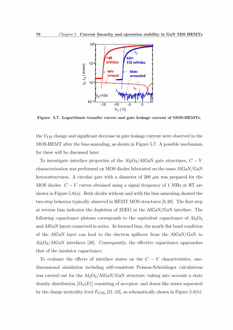
78 Chapter 5 Current linearity and operation stability in GaN MIS HEMTs
Figure 5.7. Logarithmic transfer curves and gate leakage current of MOS-HEMTs.
the VTH change and significant decrease in gate leakage current were observed in the
MOS-HEMT after the bias annealing, as shown in Figure 5.7. A possible mechanism
for these will be discussed later.
To investigate interface properties of the Al2O3/AlGaN gate structures, C − V
characterization was performed on MOS diodes fabricated on the same AlGaN/GaN
heterostructures. A circular gate with a diameter of 200 µm was prepared for the
MOS diodes. C − V curves obtained using a signal frequency of 1 MHz at RT are
shown in Figure 5.8(a). Both diodes without and with the bias annealing showed the
two-step behavior typically observed in HEMT MOS structures [8,20]. The first step
at reverse bias indicates the depletion of 2DEG at the AlGaN/GaN interface. The
following capacitance plateau corresponds to the equivalent capacitance of Al2O3
and AlGaN layers connected in series. At forward bias, the nearly flat band condition
of the AlGaN layer can lead to the electron spillover from the AlGaN/GaN to
Al2O3/AlGaN interfaces [20]. Consequently, the effective capacitance approaches
that of the insulator capacitance.
To evaluate the effects of interface states on the C − V characteristics, one-
dimensional simulation including self-consistent Poisson-Schrodinger calculations
was carried out for the Al2O3/AlGaN/GaN structure, taking into account a state
density distribution [Dit(E)] consisting of acceptor- and donor-like states separated
by the charge neutrality level ECNL [21–23], as schematically shown in Figure 5.8(b).
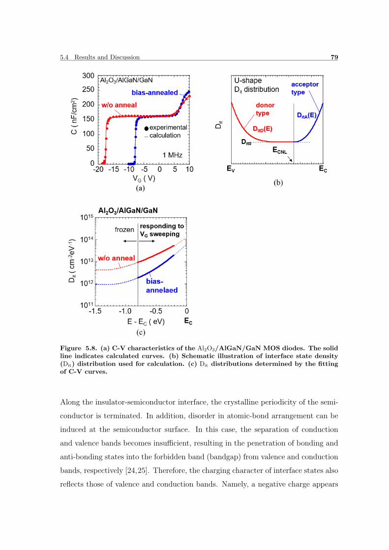
5.4 Results and Discussion 79
Figure 5.8. (a) C-V characteristics of the Al2O3/AlGaN/GaN MOS diodes. The solidline indicates calculated curves. (b) Schematic illustration of interface state density(Dit) distribution used for calculation. (c) Dit distributions determined by the fittingof C-V curves.
Along the insulator-semiconductor interface, the crystalline periodicity of the semi-
conductor is terminated. In addition, disorder in atomic-bond arrangement can be
induced at the semiconductor surface. In this case, the separation of conduction
and valence bands becomes insufficient, resulting in the penetration of bonding and
anti-bonding states into the forbidden band (bandgap) from valence and conduction
bands, respectively [24,25]. Therefore, the charging character of interface states also
reflects those of valence and conduction bands. Namely, a negative charge appears
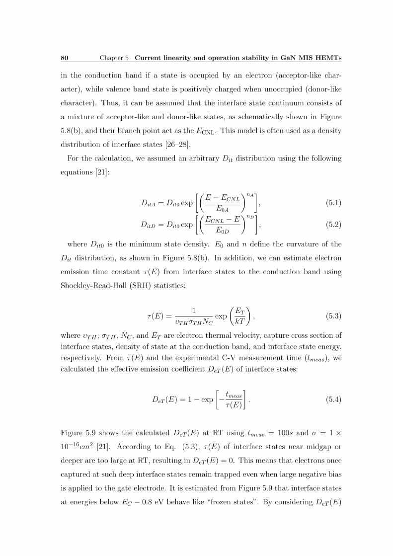
80 Chapter 5 Current linearity and operation stability in GaN MIS HEMTs
in the conduction band if a state is occupied by an electron (acceptor-like char-
acter), while valence band state is positively charged when unoccupied (donor-like
character). Thus, it can be assumed that the interface state continuum consists of
a mixture of acceptor-like and donor-like states, as schematically shown in Figure
5.8(b), and their branch point act as the ECNL. This model is often used as a density
distribution of interface states [26–28].
For the calculation, we assumed an arbitrary Dit distribution using the following
equations [21]:
DitA = Dit0 exp
[(E − ECNL
E0A
)nA], (5.1)
DitD = Dit0 exp
[(ECNL − E
E0D
)nD], (5.2)
where Dit0 is the minimum state density. E0 and n define the curvature of the
Dit distribution, as shown in Figure 5.8(b). In addition, we can estimate electron
emission time constant τ(E) from interface states to the conduction band using
Shockley-Read-Hall (SRH) statistics:
τ(E) =1
υTHσTHNC
exp
(ET
kT
), (5.3)
where υTH , σTH , NC , and ET are electron thermal velocity, capture cross section of
interface states, density of state at the conduction band, and interface state energy,
respectively. From τ(E) and the experimental C-V measurement time (tmeas), we
calculated the effective emission coefficient DeT (E) of interface states:
DeT (E) = 1− exp
[− tmeas
τ(E)
]. (5.4)
Figure 5.9 shows the calculated DeT (E) at RT using tmeas = 100s and σ = 1 ×
10−16cm2 [21]. According to Eq. (5.3), τ(E) of interface states near midgap or
deeper are too large at RT, resulting in DeT (E) = 0. This means that electrons once
captured at such deep interface states remain trapped even when large negative bias
is applied to the gate electrode. It is estimated from Figure 5.9 that interface states
at energies below EC − 0.8 eV behave like “frozen states”. By considering DeT (E)
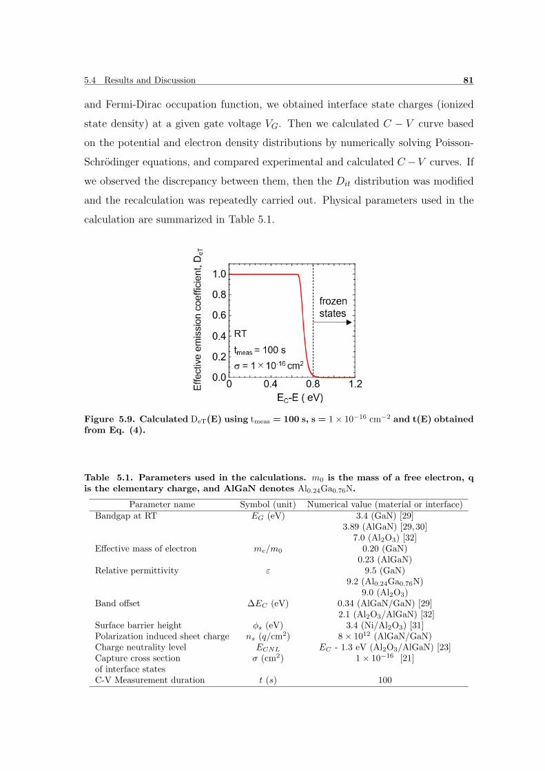
5.4 Results and Discussion 81
and Fermi-Dirac occupation function, we obtained interface state charges (ionized
state density) at a given gate voltage VG. Then we calculated C − V curve based
on the potential and electron density distributions by numerically solving Poisson-
Schrodinger equations, and compared experimental and calculated C −V curves. If
we observed the discrepancy between them, then the Dit distribution was modified
and the recalculation was repeatedly carried out. Physical parameters used in the
calculation are summarized in Table 5.1.
Figure 5.9. Calculated DeT(E) using tmeas = 100 s, s = 1× 10⁻¹⁶ cm−2 and t(E) obtainedfrom Eq. (4).
Table 5.1. Parameters used in the calculations. m0 is the mass of a free electron, qis the elementary charge, and AlGaN denotes Al0.24Ga0.76N.
Parameter name Symbol (unit) Numerical value (material or interface)Bandgap at RT EG (eV) 3.4 (GaN) [29]
3.89 (AlGaN) [29,30]7.0 (Al2O3) [32]
Effective mass of electron me/m0 0.20 (GaN)0.23 (AlGaN)
Relative permittivity ε 9.5 (GaN)9.2 (Al0.24Ga0.76N)
9.0 (Al2O3)Band offset ∆EC (eV) 0.34 (AlGaN/GaN) [29]
2.1 (Al2O3/AlGaN) [32]Surface barrier height ϕs (eV) 3.4 (Ni/Al2O3) [31]Polarization induced sheet charge ns (q/cm2) 8× 10¹² (AlGaN/GaN)Charge neutrality level ECNL EC - 1.3 eV (Al2O3/AlGaN) [23]Capture cross section σ (cm2) 1× 10⁻¹⁶ [21]of interface statesC-V Measurement duration t (s) 100
82 Chapter 5 Current linearity and operation stability in GaN MIS HEMTs
Using the Dit distributions shown in Figure 5.8(c), the calculation well reproduced
the experimental C − V data, as indicated by solid lines in Figure 5.8(a). As
described above, only the acceptor-like traps in the energy range indicated by solid
lines in Figure 5.8(c) can change their charge state accordingly with the gate voltage
sweep at RT. Note, in addition, that it is difficult to evaluate the state density
distribution at energies above EC−0.2 eV from C−V measurements using frequency
of 1 MHz, because electron trapping/detrapping processes at such shallow interface
states can respond to the measurement AC signal and accordingly give an inaccurate
estimate of capacitance. Therefore, state densities at the energies above EC − 0.2
eV were not considered for the present C − V calculation.
As shown in Figure 5.8(c), the Al2O3/AlGaN interface without annealing showed
high interface state densities of over 1× 1013 cm−2eV−1. The bias annealing process
effectively decreased the state densities, leading to the steeper C−V slope in forward
bias shown in Figure 5.8(a). The calculated VTH corresponding to the first step in
the C − V curve was -7.5 V, very close to that of the MOS-HEMT subjected to
bias annealing, as shown in Figure 5.8(a). On the other hand, the sample without
the annealing showed a VTH shift toward the negative bias direction, probably due
to excess positive charges arising from donor-type interface states and/or defect
levels in the bulk Al2O3. When a fixed charge of +1.2× 1013 cm−2 was assumed in
the Al2O3 layer or at the Al2O3/AlGaN interface, the calculation reproduced the
experimental C − V result for the HEMT without annealing, as shown in Figure
5.8(a). A possible candidate for a defect level in Al2O3 is an oxygen-vacancy related
defect [33, 34]. The bias-annealing process decreased such levels, resulting in the
VTH recovery toward the expected value. Zhou et al. [35] also reported similar VTH
recovery with a post-deposition annealing in Al2O3/AlGaN/GaN MOS-HEMTs. As
shown in Figure 5.7, in addition, we observed decrease in gate leakage current in
the MOS-HEMT after the bias annealing. For the GaN-based MIS-HEMTs using
Al2O3, SiNx and AlTiO, it has been reported that the Poole-Frenkel (PF) emission
conduction was dominant for gate leakage current [36–39]. Similarly to the VTH
recovery behavior, there is a possibility the reduction of leakage current arises from
decrease in defect levels in the Al2O3 layer, contributing to the suppression of the
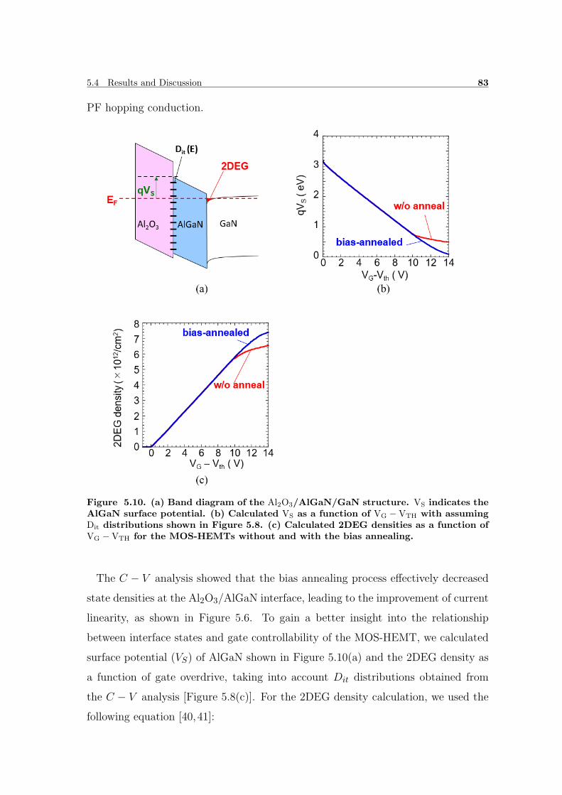
5.4 Results and Discussion 83
PF hopping conduction.
Figure 5.10. (a) Band diagram of the Al2O3/AlGaN/GaN structure. VS indicates theAlGaN surface potential. (b) Calculated VS as a function of VG −VTH with assumingDit distributions shown in Figure 5.8. (c) Calculated 2DEG densities as a function ofVG −VTH for the MOS-HEMTs without and with the bias annealing.
The C − V analysis showed that the bias annealing process effectively decreased
state densities at the Al2O3/AlGaN interface, leading to the improvement of current
linearity, as shown in Figure 5.6. To gain a better insight into the relationship
between interface states and gate controllability of the MOS-HEMT, we calculated
surface potential (VS) of AlGaN shown in Figure 5.10(a) and the 2DEG density as
a function of gate overdrive, taking into account Dit distributions obtained from
the C − V analysis [Figure 5.8(c)]. For the 2DEG density calculation, we used the
following equation [40,41]:
84 Chapter 5 Current linearity and operation stability in GaN MIS HEMTs
2DEGdensityi =mekBT
πℏ2ln [1 + exp ((Ei − Ef )/(kBT ))], (5.5)
where me is the effective electron mass, kB is Boltzman’s constant, T is the temper-
ature, and i indicates the ith discrete excited level at the AlGaN/GaN interface.
Figure 5.10(b) shows the calculated VS as a function of gate overdrive for the MOS-
HEMTs without and with the bias annealing. In the gate bias range up to 10 V, both
devices showed the same VS change. This gate voltage corresponds to qVS = 0.8 eV.
As mentioned above, interface states at energies below EC−0.8 eV are considered to
be “frozen states”, i.e., negligible effect on the VS control. Beyond VG−VTH = 10V ,
acceptor states shown in Figure 5.8(c) are active accordingly with the gate voltage
sweeping, and the ionized acceptor charges screen the gate electric field. Thus high-
density states prevent VS modulation (poor potential control) for the MOS-HEMT
without the bias annealing. Such VS behavior is directly related to the control of
the 2DEG density, as shown in Figure 5.10(c). The limited increase in the 2DEG
density with VG is clearly observed for the MOS-HEMT without the bias annealing.
On the other hand, the MOS-HEMT with annealing shows relatively good control
of 2DEG by VG. The calculated results shown in Figure 5.10(c) are similar to the
measured ID − VG curves of MOS-HEMTs shown in Figure 5.6(b), indicating that
the effective reduction of interface states is responsible for the improved linearity in
MOS-HEMT with bias annealing.
It should be mentioned that some papers reported poor current linearity in MIS-
type AlGaN/GaN HEMTs. To investigate current linearity behavior, we tried to
plot the full width at half maxima (FWHM) of gm − VG profiles as a function of
the equivalent oxide thickness (EOT) including insulator and AlGaN barrier lay-
ers. Figure 5.11 shows comparison of FWHM of gm for AlGaN/GaN MIS-HMETs
using SiO2 [42–44], Al2O3 [35, 45–48], SiN [9, 10, 49, 50], HfO2 [51, 52], AlN [53],
Ga2O3 [54] and TiO2 [55] dielectric materials. Our data are also included in Figure
5.11. It is expected that the FWHM of gm increases with EOT, and experimental
data generally showed this tendency. However, there is a wide scattering of data,
indicating that interface properties of insulator/AlGaN structures are not depen-
dent on the insulator material used but on the bond disorder and/or surface defects
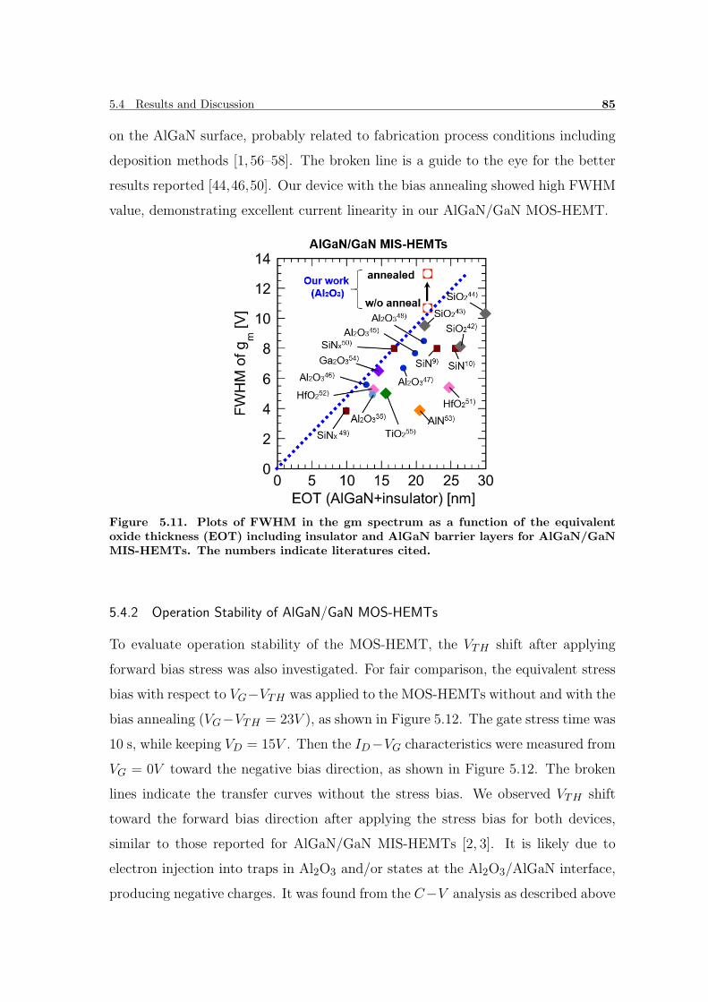
5.4 Results and Discussion 85
on the AlGaN surface, probably related to fabrication process conditions including
deposition methods [1, 56–58]. The broken line is a guide to the eye for the better
results reported [44,46,50]. Our device with the bias annealing showed high FWHM
value, demonstrating excellent current linearity in our AlGaN/GaN MOS-HEMT.
Figure 5.11. Plots of FWHM in the gm spectrum as a function of the equivalentoxide thickness (EOT) including insulator and AlGaN barrier layers for AlGaN/GaNMIS-HEMTs. The numbers indicate literatures cited.
5.4.2 Operation Stability of AlGaN/GaN MOS-HEMTs
To evaluate operation stability of the MOS-HEMT, the VTH shift after applying
forward bias stress was also investigated. For fair comparison, the equivalent stress
bias with respect to VG−VTH was applied to the MOS-HEMTs without and with the
bias annealing (VG−VTH = 23V ), as shown in Figure 5.12. The gate stress time was
10 s, while keeping VD = 15V . Then the ID−VG characteristics were measured from
VG = 0V toward the negative bias direction, as shown in Figure 5.12. The broken
lines indicate the transfer curves without the stress bias. We observed VTH shift
toward the forward bias direction after applying the stress bias for both devices,
similar to those reported for AlGaN/GaN MIS-HEMTs [2, 3]. It is likely due to
electron injection into traps in Al2O3 and/or states at the Al2O3/AlGaN interface,
producing negative charges. It was found from the C−V analysis as described above
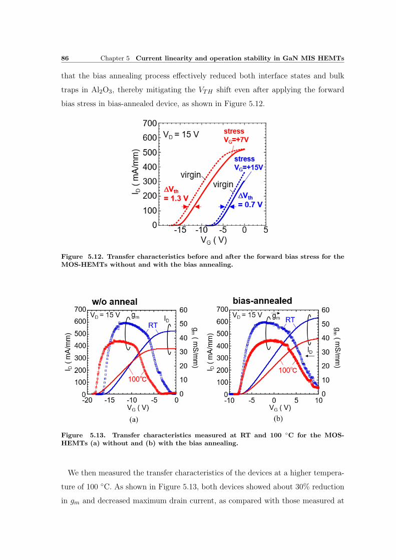
86 Chapter 5 Current linearity and operation stability in GaN MIS HEMTs
that the bias annealing process effectively reduced both interface states and bulk
traps in Al2O3, thereby mitigating the VTH shift even after applying the forward
bias stress in bias-annealed device, as shown in Figure 5.12.
Figure 5.12. Transfer characteristics before and after the forward bias stress for theMOS-HEMTs without and with the bias annealing.
Figure 5.13. Transfer characteristics measured at RT and 100 C for the MOS-HEMTs (a) without and (b) with the bias annealing.
We then measured the transfer characteristics of the devices at a higher tempera-
ture of 100 C. As shown in Figure 5.13, both devices showed about 30% reduction
in gm and decreased maximum drain current, as compared with those measured at
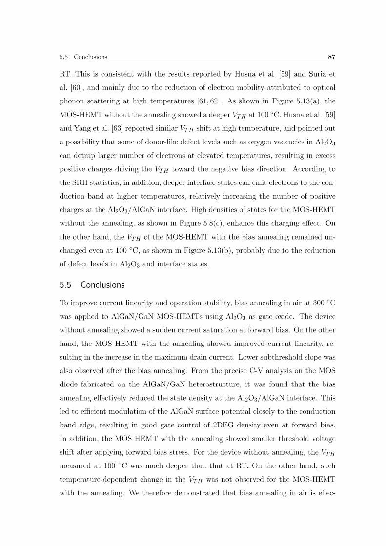
5.5 Conclusions 87
RT. This is consistent with the results reported by Husna et al. [59] and Suria et
al. [60], and mainly due to the reduction of electron mobility attributed to optical
phonon scattering at high temperatures [61, 62]. As shown in Figure 5.13(a), the
MOS-HEMT without the annealing showed a deeper VTH at 100 C. Husna et al. [59]
and Yang et al. [63] reported similar VTH shift at high temperature, and pointed out
a possibility that some of donor-like defect levels such as oxygen vacancies in Al2O3
can detrap larger number of electrons at elevated temperatures, resulting in excess
positive charges driving the VTH toward the negative bias direction. According to
the SRH statistics, in addition, deeper interface states can emit electrons to the con-
duction band at higher temperatures, relatively increasing the number of positive
charges at the Al2O3/AlGaN interface. High densities of states for the MOS-HEMT
without the annealing, as shown in Figure 5.8(c), enhance this charging effect. On
the other hand, the VTH of the MOS-HEMT with the bias annealing remained un-
changed even at 100 C, as shown in Figure 5.13(b), probably due to the reduction
of defect levels in Al2O3 and interface states.
5.5 Conclusions
To improve current linearity and operation stability, bias annealing in air at 300 C
was applied to AlGaN/GaN MOS-HEMTs using Al2O3 as gate oxide. The device
without annealing showed a sudden current saturation at forward bias. On the other
hand, the MOS HEMT with the annealing showed improved current linearity, re-
sulting in the increase in the maximum drain current. Lower subthreshold slope was
also observed after the bias annealing. From the precise C-V analysis on the MOS
diode fabricated on the AlGaN/GaN heterostructure, it was found that the bias
annealing effectively reduced the state density at the Al2O3/AlGaN interface. This
led to efficient modulation of the AlGaN surface potential closely to the conduction
band edge, resulting in good gate control of 2DEG density even at forward bias.
In addition, the MOS HEMT with the annealing showed smaller threshold voltage
shift after applying forward bias stress. For the device without annealing, the VTH
measured at 100 C was much deeper than that at RT. On the other hand, such
temperature-dependent change in the VTH was not observed for the MOS-HEMT
with the annealing. We therefore demonstrated that bias annealing in air is effec-

88 Chapter 5 Current linearity and operation stability in GaN MIS HEMTs
tive in improving current linearity and operation stability of Al2O3/AlGaN/GaN
MOS-HEMTs.
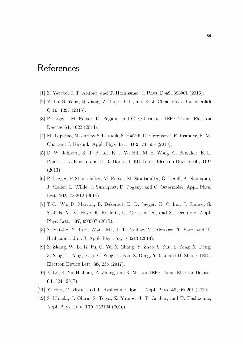
89
References
[1] Z. Yatabe, J. T. Asubar, and T. Hashizume, J. Phys. D 49, 393001 (2016).
[2] Y. Lu, S. Yang, Q. Jiang, Z. Tang, B. Li, and K. J. Chen, Phys. Status Solidi
C 10, 1397 (2013).
[3] P. Lagger, M. Reiner, D. Pogany, and C. Ostermaier, IEEE Trans. Electron
Devices 61, 1022 (2014).
[4] M. Tapajna, M. Jurkovic, L. Valik, S. Hascik, D. Gregusova, F. Brunner, E.-M.
Cho, and J. Kuzmik, Appl. Phys. Lett. 102, 243509 (2013).
[5] D. W. Johnson, R. T. P. Lee, R. J. W. Hill, M. H. Wong, G. Bersuker, E. L.
Piner, P. D. Kirsch, and H. R. Harris, IEEE Trans. Electron Devices 60, 3197
(2013).
[6] P. Lagger, P. Steinschifter, M. Reiner, M. Stadtmuller, G. Denifl, A. Naumann,
J. Muller, L. Wilde, J. Sundqvist, D. Pogany, and C. Ostermaier, Appl. Phys.
Lett. 105, 033512 (2014).
[7] T.-L. Wu, D. Marcon, B. Bakeroot, B. D. Jaeger, H. C. Lin, J. Franco, S.
Stoffels, M. V. Hove, R. Roelofts, G. Groeseneken, and S. Decoutere, Appl.
Phys. Lett. 107, 093507 (2015).
[8] Z. Yatabe, Y. Hori, W.-C. Ma, J. T. Asubar, M. Akazawa, T. Sato, and T.
Hashizume: Jpn. J. Appl. Phys. 53, 100213 (2014).
[9] Z. Zhang, W. Li, K. Fu, G. Yu, X. Zhang, Y. Zhao, S. Sun, L. Song, X. Deng,
Z. Xing, L. Yang, R. Ji, C. Zeng, Y. Fan, Z. Dong, Y. Cai, and B. Zhang, IEEE
Electron Device Lett. 38, 236 (2017).
[10] X. Lu, K. Yu, H. Jiang, A. Zhang, and K. M. Lau, IEEE Trans. Electron Devices
64, 824 (2017).
[11] Y. Hori, C. Mizue, and T. Hashizume, Jpn. J. Appl. Phys. 49, 080201 (2010).
[12] S. Kaneki, J. Ohira, S. Toiya, Z. Yatabe, J. T. Asubar, and T. Hashizume,
Appl. Phys. Lett. 109, 162104 (2016).
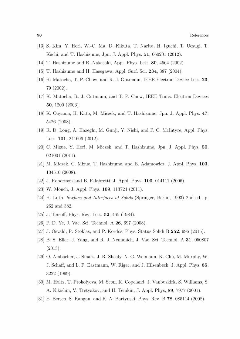
90 References
[13] S. Kim, Y. Hori, W.-C. Ma, D. Kikuta, T. Narita, H. Iguchi, T. Uesugi, T.
Kachi, and T. Hashizume, Jpn. J. Appl. Phys. 51, 060201 (2012).
[14] T. Hashizume and R. Nakasaki, Appl. Phys. Lett. 80, 4564 (2002).
[15] T. Hashizume and H. Hasegawa, Appl. Surf. Sci. 234, 387 (2004).
[16] K. Matocha, T. P. Chow, and R. J. Gutmann, IEEE Electron Device Lett. 23,
79 (2002).
[17] K. Matocha, R. J. Gutmann, and T. P. Chow, IEEE Trans. Electron Devices
50, 1200 (2003).
[18] K. Ooyama, H. Kato, M. Miczek, and T. Hashizume, Jpn. J. Appl. Phys. 47,
5426 (2008).
[19] R. D. Long, A. Hazeghi, M. Gunji, Y. Nishi, and P. C. McIntyre, Appl. Phys.
Lett. 101, 241606 (2012).
[20] C. Mizue, Y. Hori, M. Miczek, and T. Hashizume, Jpn. J. Appl. Phys. 50,
021001 (2011).
[21] M. Miczek, C. Mizue, T. Hashizume, and B. Adamowicz, J. Appl. Phys. 103,
104510 (2008).
[22] J. Robertson and B. Falabretti, J. Appl. Phys. 100, 014111 (2006).
[23] W. Monch, J. Appl. Phys. 109, 113724 (2011).
[24] H. Luth, Surface and Interfaces of Solids (Springer, Berlin, 1993) 2nd ed., p.
262 and 382.
[25] J. Tersoff, Phys. Rev. Lett. 52, 465 (1984).
[26] P. D. Ye, J. Vac. Sci. Technol. A 26, 697 (2008).
[27] J. Osvald, R. Stoklas, and P. Kordos, Phys. Status Solidi B 252, 996 (2015).
[28] B. S. Eller, J. Yang, and R. J. Nemanich, J. Vac. Sci. Technol. A 31, 050807
(2013).
[29] O. Ambacher, J. Smart, J. R. Shealy, N. G. Weimann, K. Chu, M. Murphy, W.
J. Schaff, and L. F. Eastmann, W. Riger, and J. Hilsenbeck, J. Appl. Phys. 85,
3222 (1999).
[30] M. Holtz, T. Prokofyeva, M. Seon, K. Copeland, J. Vanbuskirk, S. Williams, S.
A. Nikishin, V. Tretyakov, and H. Temkin, J. Appl. Phys. 89, 7977 (2001).
[31] E. Bersch, S. Rangan, and R. A. Bartynski, Phys. Rev. B 78, 085114 (2008).
91
[32] T. Hashizume, S. Ootomo, T. Inagaki, and H. Hasegawa, J. Vac. Sci. Technol.
B 21, 1828 (2003).
[33] P. Jonnard, C. Bonnelle, G. Blaise, G. Remond, and C. Roques-Carmes, J.
Appl. Phys. 88, 6413 (2000).
[34] M. Choi, J. L. Lyons, A. Janotti, and C. G. Van de Walle, Phys. Status Solidi
B 250, 787 (2013).
[35] H. Zhou, G. I. Ng, Z. H. Liu, and S. Arulkumaran, Appl. Phys. Express 4,
104102 (2011).
[36] H. Liu, W. Hsu, C. Lee, B. Chou, Y. Liao, and M. Chiang, IEEE Trans. Electron
Devices 61, 2760 (2014).
[37] S. Le, T. Ui, T. Q. Nguyen, H. Shih, and T. Suzuki, J. Appl. Phys. 119, 204503
(2016).
[38] M. Hua, C. Liu, S. Yang, S. Liu, K. Fu, Z. Dong, Y. Cai, B. Zhang, and K. J.
Chen, IEEE Trans. Electron Devices 62, 3215 (2015).
[39] S. A. Jauss, K. Hallaceli, S. Mansfeld, S. Schwaiger, W. Daves, and O. Ambacer,
IEEE Trans. Electron Devices 64, 2298 (2017).
[40] L. Gordon, M. Miao, S. Chowdhury, M. Higashiwaki, U. K. Mishra, and CG
Van de Walle, J Phys. D 43, 505501 (2010).
[41] M. Zervos, A. Kostopoulos, G. Constantinidis, M. Kayambaki, and A. Geor-
gakilas, J. Appl. Phys. 91, 4387 (2002).
[42] M. A. Khan, X. Hu, G. Sumin, A. Lunev, J. Yang, R. Gaska, and M. S. Shur,
IEEE Electron Device Lett. 21, 63 (2000).
[43] D. Mistele, T. Rotter, K.S. Rover, S. Paprotta, M. Seyboth, V. Schwegler, F.
Fedler, H. Klausing, O.K. Semchinova, J. Stemmer, J. Aderhold, and J. Graul,
Mater. Sci. Eng. B 93, 107 (2002).
[44] L. Pang, Y. Lian, D. Kim, J.-H. Lee, and K. Kim, IEEE Trans. Electron Devices
59, 2650 (2012).
[45] P. D. Ye, B. Yang, K. K. Ng, J. Bude, G. D. Wilk, S. Halder, and J. C. M.
Hwang, Appl. Phys. Lett. 86, 063501 (2005).
[46] D. J. Meyer, R. Bass, D. S. Katzer, D. A. Deen, S. C. Binari, K. M. Daniels,
and C. R. Eddy, Jr., Solid-State Electron. 54, 1098 (2010).
92 References
[47] E. Miyazaki, Y. Goda, S. Kishimoto, and T. Mizutani, Solid-State Electron.
62, 152 (2011).
[48] F. Sang, M. Wang, C. Zhang, M. Tao, B. Xie, C. P. Wen, J. Wang, Y. Hao, W.
Wu, and B. Shen, Jpn. J. Appl. Phys. 54, 044101 (2015).
[49] K. Zhang, M. Wu, X. Lei, W. Chen, X. Zheng, X. Ma, and Y. Hao, Semicond.
Sci. Technol. 29, 075019 (2014).
[50] H. Jiang, C. Liu, Y. Chen, X. Lu, C. W. Tang, and K. M. Lau: IEEE Trans.
Electron Devices 64, 832 (2017).
[51] S. Sugiura, Y. Hayashi, S. Kishimoto, T. Mizutani, M. Kuroda, T. Ueda, T.
Tanaka, Solid-State Electron. 54, 79 (2010).
[52] O. Seok, W. Ahn, M.-K. Han, and M.-W. Ha, Semicond. Sci. Technol. 28,
025001 (2013).
[53] J.-J. Zhu, X.-H. Ma, Y. Xie, B. Hou, W.-W. Chen, J.-C. Zhang, and Y. Hao,
IEEE Trans. Electron Devices 62, 512 (2015).
[54] H.-Y. Shih, F.-C. Chu, A. Das, C.-Y. Lee, M.-J. Chen, and R.-M. Lin, Nanoscale
Res. Lett. 11, 235 (2016).
[55] Y.-S. Lin and C.-C. Lu, J. Vac. Sci. Technol. B 35, 011209 (2017).
[56] T. Hashizume and R. Nakasaki, Appl. Phys. Lett. 80, 4564 (2002).
[57] T. Hashizume and H. Hasegawa, Appl. Surf. Sci. 234, 387 (2004).
[58] S. Kim, Y. Hori, W.-C. Ma, D. Kikuta, T. Narita, H. Iguchi, T. Uesugi, T.
Kachi, and T. Hashizume, Jpn. J. Appl. Phys. 51, 060201 (2012).
[59] F. Husna, M. Lachab, M. Sultana, V. Adivarahan, Q. Fareed, and A. Khan,
IEEE Trans. Electron Devices 59, 2424 (2012).
[60] A. J Suria, A. S. Yalamarthy, H. So, and D. G Senesky, Semicond. Sci. Technol.
31, 115017 (2016).
[61] W.S. Tan, M.J. Uren, P.W. Fry, P.A. Houston, R.S. Balmer, and T. Martin,
Solid-State Electron. 50, 511 (2006).
[62] Y.-H. Wang, Y. C Liang, G. S Samudra, T.-F. Chang, C. Huang, L. Yuan, and
G.-Q. Lo, Semicond. Sci. Technol. 28, 125010 (2013).
[63] S. Yang, S. Liu, C. Liu, M. Hua, and K. J Chen, Semicond. Sci. Technol. 31,
024001 (2016).
93
Chapter 6
Conclusion
This thesis aimed at the evaluation the effect of interface states on the electronic
characterization of AlGaN/GaN HEMTs and to control the interface state density
at Al2O3/AlGaN or Al2O3/GaN interfaces.
Chapter 1 started with the introduction of wireless mobile communication systems
which are widely used all over the world. GaN and related materials are attractive
for the application to the semiconductor devices owing to their superior physical
properties. In addition, GaN-related High Electron Mobility Transistors (HEMTs)
are very attractive for such devices. However, it is rather difficult to characterize and
control electronic states, in particular, at the insulator/semiconductor interfaces in
the insulated-gate GaN transistors because of their wide bandgap and complicated
structure having two (or more) interfaces.
Chapter 2 explained the physical properties of III-N semiconductors and their het-
erostructures, followed by the generation of two-dimensional electron gas (2DEG).
2DEG is generated by spontaneous and piezoelectric polarization charges. Such po-
larization charges were calculated from some constants of GaN and AlN. Finally,
2DEG density vs AlGaN thickness was calculated.
Chapter 3 discussed basic theories on the electronic states at the Semiconductor
surface and Insulator/Semiconductor interface. The models of “Metal-Induced-Gap-
State (MIGS)” and “Disorder-Induced-Gap-State (DIGS)” were described. In addi-
tion, the equations from DIGS model to calculate interface state density distributions
were described. To evaluate the effect of interface sates on potential distribution and
C-V characteristics of Al2O3/GaN MOS diodes. Finally, “reverse-bias annealing”
to control the interface state density was proposed.
Chapter 4 introduced the experimental results obtained for this thesis. The dual-
94 Chapter 6 Conclusion
gate AlGaN/GaN HEMTs were fabricated to evaluate the surface charging area. In
G2-stress/G1-drive scheme, the VTH was shifted toward forward bias direction. To
shed a light this phenomenon, the two-dimensional simulation was carried out. The
2D potential simulation indicated that surface negative charges induced by the G1
stress modulate the potential distribution in the AlGaN barrier layer near the G2
edge where the potential near the surface of the AlGaN barrier layer are apparently
bended and lifted. Consequently, this may lead to a decreased 2DEG concentration
in this region and eventually shifting of the VTH towards positive voltage direction.
It was also found that such surface charging can extend as far as 0.5 µm from the
stressing gate edge.
Chapter 5 investigated the relationship between the interface state densities and
the electrical properties of the Al2O3/AlGaN/GaN MOS HEMTs. The “reverse-bias
annealing” was also applied to the MOS HEMTs for reducing the Al2O3/AlGaN
interface. The device without annealing showed a sudden current saturation at
forward bias. On the other hand, the MOS HEMT with the annealing showed im-
proved current linearity, resulting in the increase in the maximum drain current.
Lower subthreshold slope was also observed after the bias annealing. From the pre-
cise C-V analysis on the MOS diode fabricated on the AlGaN/GaN heterostructure,
it was found that the bias annealing effectively reduced the state density at the
Al2O3/AlGaN interface. This led to efficient modulation of the AlGaN surface po-
tential closely to the conduction band edge, resulting in good gate control of 2DEG
density even at forward bias. In addition, the MOS HEMT with the annealing
showed smaller threshold voltage shift after applying forward bias stress. For the
device without annealing, the VTH measured at 100 C was much deeper than that
at RT. On the other hand, such temperature-dependent change in the VTH was
not observed for the MOS-HEMT with the annealing. We therefore demonstrated
that bias annealing in air is effective in improving current linearity and operation
stability of Al2O3/AlGaN/GaN MOS-HEMTs.
95
List of publications/conferences/awards
Publications
Journals
1. KenyaNishiguchi, Joel T. Asubar and T. Hashizume, “Evaluation of off-bias-
stress induced surface charging at AlGaN/GaN surface using a dual-gate tran-
sistor structure”, Japanese Journal of Applied Physics, Vol. 53, pp. 070301-1-4
(2014). (IF=1.384, TC=2)
2. KenyaNishiguchi, Syota Kaneki, Shiro Ozaki, and Tamotsu Hashizume, “Cur-
rent linearity and operation stability in Al2O3-gate AlGaN/GaN MOS high
electron mobility transistors”, Japanese Journal of Applied Physics, Vol. 56,
pp. 101001-1-8 (2017). (IF=1.384, TC=0)
Proceedings
1. KenyaNishiguchi and Tamotsu Hashizume,“Surface charging effects on current
stability of AlGaN/GaN HEMTs”, Proc. of The 2014 International Meeting
for Future of Electron Devices, Kansai (IMFEDK), pp. 66-67 (2014).
2. KenyaNishiguchi, Joel T. Asubar, N. Tamaki, and Tamotsu Hashizume,“Eval-
uation of surface charging at AlGaN surface using dual-gate structure”, Proc.
of The 11th Topical Workshop on Heterostructure Microelectronics (TWHM),
pp. 19-20 (2015).
3. KenyaNishiguchi, Shota Kaneki, and Tamotsu Hashizume, “Effects of bias
annealing on current linearity of Al2O3/AlGaN/GaN MOS HEMTs”, Proc.
of The 12th Topical Workshop on Heterostructure Microelectronics (TWHM),
pp. 21-22 (2017).
96 List of publications/conferences/awards
Journals related to this study
1. Kota Ohi, Joel Tacla Asubar, KenyaNishiguchi, and Tamotsu Hashizume,
“Current Stability in Multi-Mesa-Channel AlGaN/GaN HEMTs”, IEEE
Transactions on Electron Devices, Vol. 60, No. 10, pp. 2997-3004 (2013).
2. Joel Asubar, Kota Ohi, KenyaNishiguchi, and Tamotsu Hashizume,“Improved
current stability in multi-mesa-channel AlGaN/GaN transistors”, Physica Sta-
tus Solidi C, Vol. 11, No. 3-4, pp. 857-861 (2014).
3. Shiro Ozaki, Kozo Makiyama, Toshihiro Ohki, Naoya Okamoto, Shota Kaneki,
KenyaNishiguchi, Naoki Hara, and Tamotsu Hashizume, “Effects of air anneal-
ing on DC characteristics of InAlN/GaN MOS high-electron-mobility transis-
tors using atomic-layer-deposited Al2O3”, Applied Physics Express, Vol. 10,
No. 6, pp. 061001-1-4 (2017).
4. Tamotsu Hashizume, KenyaNishiguchi, Shota Kaneki, Jan Kuzmik, and Zenji
Yatabe, ”State of the art on gate insulation and surface passivation for GaN-
based power HEMTs”, Materials Science in Semiconductor Processing, 掲載
決定 (2018年 4月公表予定)
Conferences
International conferences
1. KenyaNishiguchi and Tamotsu Hashizume,“Surface charging effects on current
stability of AlGaN/GaN HEMTs”, The 2014 International Meeting for Future
of Electron Devices, Kansai (IMFEDK), PB-08, Kyoto, Japan, June 19-20,
2014.
2. KenyaNishiguchi, Joel T. Asubar and Tamotsu Hashizume,“Spatial discrim-
ination of surface charging region in AlGaN/GaN HEMTs investigated using
dual-gate architecture”, The International Workshop on Nitride Semiconduc-
tors (IWN), WeEP2, Wrocaw, Poland, August 24-29, 2014.
3. KenyaNishiguchi, Joel T. Asubar, N. Tamaki, and Tamotsu Hashizume,
“Evaluation of surface charging at AlGaN surface using dual-gate structure”,
11th Topical Workshop on Heterostructure Microelectronics (TWHM), 2-6,
97
Takayama, Japan, August 23-26, 2015.
4. KenyaNishiguchi, Joel T. Asubar, N. Tamaki, and Tamotsu Hashizume,“Con-
trollability improvement of Al2O3-gate structure for GaN transistors”, Com-
pound Semiconductor Week (CSW), WeB2-2, Toyama, Japan, June 26-30,
2016.
5. KenyaNishiguchi, Syota Kaneki, and Tamotsu Hashizume, ”Improving Gate
controllability of AlGaN/GaN MOS HEMTs”, 12th International Conference
on Nitride Semiconductors (ICNS), C 2.3, Strasbourg, France, July 24-28,
2017.
6. KenyaNishiguchi, Joel T. Asubar, N. Tamaki, and Tamotsu Hashizume,
”Effects of bias annealing on current linearity of Al2O3/AlGaN/GaN MOS
HEMTs”, 12th Topical Workshop on Heterostructure Microelectronics
(TWHM), 3-6, Kirishima, Kyushuu, Japan, August 28-31, 2017.
Domestic conferences
1. 西口賢弥, Joel T. Asubar,橋詰保, “デュアルゲート構造によるAlGaN/GaN
HEMTの電流コラプス評価”, 第 74回応用物理学会秋季学術講演会, 20a-
D7-11, 同志社大学, 平成 25年 9月.
2. 西口賢弥, Joel T. Asubar,橋詰保, “デュアルゲート構造によるAlGaN/GaN
HEMTのオフ状態ストレスによる電流変動評価”, 第 49回応用物理学会北
海道支部学術講演会, A-20, 北海道大学, 平成 25年 12月.
3. 西口賢弥, Joel T. Asubar, 橋詰保, “AlGaN/GaN HEMTにおけるオフスト
レス後の電流変動評価”, 第 61回応用物理学会春季学術講演会, 19a-D8-5,
青山大学, 平成 26年 3月.
4. 西口賢弥, Joel T. Asubar, 橋詰保, “AlGaN/GaN HEMTにおけるオフ状
態ストレス後の表面帯電評価”, 第 62 回応用物理学会春季学術講演会,
12p-A21-10, 東海大学, 平成 27年 3月.
5. 西口賢弥, 橋詰保, “高温アニールプロセスがGaN MOSFET特性に与える
影響”, 第 63回応用物理学会春季学術講演会, 22a-W541-6, 東京工業大学,
平成 28年 3月.
6. 西口賢弥, 橋詰保, “GaNキャップ層が AlGaN/GaN MOS構造の C-V特性
98 List of publications/conferences/awards
に与える影響”, 第 64回応用物理学会春季学術講演会, 16a-P4-10, パシフィ
コ横浜, 平成 29年 3月.
7. 西口賢弥, 金木 奨太, 橋詰保, “Al2O3膜を用いたAlGaN/GaN MOS HEMT
の電流制御性向上”,第 78回応用物理学会秋季学術講演会, 7p-S22-4, 福岡
国際会議場, 平成 29年 9月.
Awards
1. “第 17回応用物理学会北海道支部発表奨励賞” 西口賢弥, Joel T. Asubar,
橋詰保, “デュアルゲート構造によるAlGaN/GaN HEMTのオフ状態スト
レスによる電流変動評価”, 平成 25年 12月.