Embed Size (px)
Citation preview

Université catholique de Louvain Ecole Polytechnique de Louvain ICTEAM Institute of Information and Communication Technologies, Electronics and Applied Mathematics
Theoretical and Experimental Study
of Innovative Thin-Film Gated SOI
Lateral PIN Optoelectronic Device
Guoli Li
Thesis submitted in partial fulfillment of the requirements for the degree of Docteur en Sciences de l’Ingénieur
Dissertation Committee:
Prof. Denis Flandre (Supervisor) Université catholique de Louvain, Belgium
Prof. Yun Zeng (Supervisor)
Hunan University, China
Prof. Laurent Francis (President)
Université catholique de Louvain, Belgium
Prof. Chujun Zhao (Member)
Hunan University, China
Dr. Nicolas Reckinger (Member) Université de Namur, Belgium
Dr. Nicolas André (Secretary) Université catholique de Louvain, Belgium
July 2017

To my family
To my friends
To myself

“Be thankful for who you are and what you have; you'll end up having
more.”
Contents
Acknowledgements ....................................................................................... i
Abstract .......................................................................................................... iii
Publications ................................................................................................... vi
List of acronyms ........................................................................................ viii
List of symbols .............................................................................................. xi
Introduction ................................................................................................... 1
CHAPTER 1 State-of-the-art optical detection ................................... 5
1.1 Optical-electrical conversion in semiconductors .................................................... 6
1.1.1 Intrinsic and extrinsic transitions ......................................................................... 6
1.1.2 Direct and indirect transitions ............................................................................... 8
1.1.3 Light absorption and penetration ......................................................................... 9
1.1.4 Recombination mechanism ................................................................................... 11
1.2 Fundamental physics in PN junction .......................................................................... 12
1.2.1 PN junction under bias ............................................................................................ 13
1.2.2 Current-voltage characteristics ........................................................................... 14
1.2.3 PN junction for thermal and optical sensing................................................... 17
1.2.4 A lateral PIN photodiode ........................................................................................ 18
1.2.5 Device performance metrics ................................................................................. 20
1.3 Technology and applications in optical sensor ...................................................... 22
1.3.1 A 1.0 μm SOI CMOS technology ............................................................................ 22
1.3.2 Applications for optical sensor ............................................................................ 24
CHAPTER 2 Electrical optimization in a gated SOI lateral PIN diode............................................................................................................... 27
2.1 A conceptual ITO-gated SOI lateral PIN diode ........................................................ 28
2.1.1 Schematic diagram .................................................................................................... 28
2.1.2 Full depletion case .................................................................................................... 29
2.2 Device performance in Atlas/SILVACO simulation .............................................. 31
2.2.1 Device dark current .................................................................................................. 32
2.2.2 Device optical response .......................................................................................... 34
2.2.2.1 Effect of gate and reverse biases ................................................................. 34
2.2.2.2 Intrinsic length variation ............................................................................... 37
2.2.2.3 Doping concentration variation .................................................................. 39

2.2.2.4 Varied incident wavelength .......................................................................... 41
2.3 An experimental Al-gated SOI lateral PIN diode .................................................... 42
2.3.1 Device geometry ........................................................................................................ 42
2.3.2 Depletion regime with back gate bias ............................................................... 43
2.3.3 Experimental characterization ............................................................................. 45
2.3.3.1 Fully-depleted condition by back-gate bias ............................................ 46
2.3.3.2 Non-fully-depleted (NFD) regime ............................................................... 47
2.4 Summary ............................................................................................................................... 48
CHAPTER 3 Device degradation and local annealing ................... 50
3.1 Device fabrication and operation ................................................................................ 51
3.1.1 Micro-hotplate platform and MEMS post-processing ................................. 51
3.1.2 Available SOI lateral PIN (P+/P–/N+) diodes ................................................... 53
3.1.3 Local annealing operation ...................................................................................... 55
3.2 Process-induced degradation and local-annealing improvement .................. 57
3.2.1 Diode forward characteristics .............................................................................. 57
3.2.1.1 After DRIE ............................................................................................................ 60
3.2.1.2 With Al deposition and back gate influence ........................................... 63
3.2.1.3 Device stability in forward condition ........................................................ 65
3.2.2 Reverse leakage current ......................................................................................... 66
3.2.2.1 Without gate bias .............................................................................................. 68
3.2.2.2 Under gate biasing ............................................................................................ 69
3.2.3 Optical response ........................................................................................................ 71
3.2.4 Carriers’ lifetime and surface recombination velocity ................................ 73
3.2.5 Low-frequency noise characterization ............................................................. 74
3.3 Simulation and analysis of diode reverse leakage current ................................ 77
3.3.1 A suspended SOI PIN diode without gate ......................................................... 77
3.3.2 A suspended SOI PIN diode with traps and gate bias .................................. 79
3.3.2.1 Two-dimensional device model in Atlas/SILVACO .............................. 80
3.3.2.2 On-membrane suspended device M10 without annealing ............... 81
3.3.2.3 On-membrane suspended device M10 after annealing ..................... 86
3.4 Summary ............................................................................................................................... 88
CHAPTER 4 Optical optimization in a SOI lateral PIN diode ...... 90
4.1 Light propagation in multilayer stack films ............................................................ 91
4.1.1 Transfer matrix method .......................................................................................... 91
4.1.2 Reflectance, transmittance and absorption .................................................... 93
4.2 Device optical simulations with transfer matrix method................................... 94

4.2.1 With gold bottom reflector .................................................................................... 94
4.2.2 With aluminum backside reflector ..................................................................... 99
4.3 Experimental characterization of device responsivity .................................... 101
4.3.1 Measurement set-up at room temperature .................................................. 101
4.3.2 Responsivity versus intrinsic length ............................................................... 102
4.3.3 Responsivity versus backside reflectors ....................................................... 104
4.4 Light discrimination and high-temperature applications ............................... 107
4.4.1 Multiple-wavelength detection ......................................................................... 107
4.4.2 High-temperature application ........................................................................... 109
4.5 Summary ............................................................................................................................ 112
CHAPTER 5 An innovative graphene-gated SOI lateral PIN diode ........................................................................................................................ 113
5.1 Device fabrication process .......................................................................................... 114
5.1.1 XeF2 silicon substrate etch .................................................................................. 114
5.1.2 Graphene transfer process.................................................................................. 117
5.1.3 Chip-on-board technology .................................................................................. 121
5.2 Electrical characterization in dark condition ...................................................... 123
5.3 Device optical response ................................................................................................ 125
5.3.1 In the visible (VS) wavelength range .............................................................. 125
5.3.2 In the ultraviolet (UV) wavelength range ..................................................... 127
5.3.3 Simulation analysis in absorption .................................................................... 128
5.3.4 Under graphene-gate bias ................................................................................... 130
5.4 Summary ............................................................................................................................ 132
CHAPTER 6 Summary and perspectives ......................................... 133
6.1 Summary ............................................................................................................................ 133
6.2 Perspectives ...................................................................................................................... 135
Bibliography .............................................................................................. 139
Annex 1: Reverse- and forward-biased gated-diode technique ........................................................................................................................ 148
Annex 2: A typical distribution of interface trap density (Dit) . 153

i
Acknowledgements
This thesis was firstly started in Hunan University, China, then proceeded forward and turned to be a joint PhD program between Université catholique de Louvain (UCL), Belgium and Hunan University (HNU), China. Continuous support and encouragements from the many following people were really important for me during the past four years.
First, I would like to express my sincere and deepest gratitudes to my supervisors Prof. Denis Flandre and Prof. Yun Zeng. Great and continuous support from Prof. Zeng brought me the opportunity to pursue my thesis research at UCL and the joint PhD program, and always encouraged me during the PhD period. The professional supervision and guidance from Prof. Flandre greatly helped me all the time in my research at UCL. In particular, his patient explanation of the theory foundations and fruitful discussions, his careful reading of my writings and his immense knowledge always go to the professional advices in my research. His trust, support and encouragement were also indeed important to me during my stay at UCL.
Second, my profound gratitudes go to the China Scholarship Council (CSC) and the Conseil de l'Action internationale (CIA) of UCL for the funding of my PhD study, and the European project SOI-HITS for providing the samples for my thesis, and the two Universities UCL and HNU for the collaboration and cooperation.
My special thanks go to Dr. Nicolas André (UCL) for his mentorship and countless insightful suggestions in research, and for the personal support and tight friendship. I also would like to sincerely thank Prof. Laurent A. Francis (UCL) for supporting my joint PhD program as a member of the committee and leading the Jury; to Prof. Chujun Zhao (HNU) for participating in my thesis work and being a member of the Jury; to Dr. Nicolas Reckinger (Université de Namur) for the generous offer of graphene flakes and his professional guidance, and the scientific collaboration; and to Dr. Wanghui Zou (HNU) for the guidance in the very first year of my PhD period.
I also wish to appreciate Dr. Olivier Poncelet, Dr. Valeriya Kilchytska and Dr. Xiaohui Tang for their useful scientific discussions and information. In addition, I want to express my sincere thanks to Mr. Pascal Simon for his training and help in Welcome platform; Mr. Miloud Zitoud and Mr. Pierre Gérard for technical assistance; Mr. Christian Renaux, Mrs. Ester Tooten for the guidance and support in Winfab platform (UCL).

ii
My gratitude also goes to Ir. Yu Xia for her participation in my research and the personally continuous help while I was abroad. My warm regards go to my charming office colleagues, Dr. Ratan Kotipalli, Ir. Maria Zhukova, Ir. Bin Wang, and also Mrs. Viviane Sauvage, Mrs Samia Patsalides and Mrs. Juan Zhao for the administrative assistance at UCL and HNU.
Finally, I would like to gratefully thank my beloved parents, my mother Dongmei Huang and father Shengzhu Li, for supporting me spiritually throughout the doctoral period and my life in general, and also my big family and my dear friends in China and Belgium.
Guoli

iii
Abstract
ilicon-on-insulator (SOI) lateral P+/P
-/N
+ (PIN) diode has triggered large interests
and perspectives for optical sensing, thanks to its demonstrated superior performances
such as low leakage current. To extend the optical sensing capability of the SOI lateral
PIN diode within the ultraviolet, visible and near infrared wavelength ranges, improve
the optical response and optimize the device electrical and optical performances, this
thesis comprehensively and deeply investigates the electrical and optical performance
of the SOI lateral PIN diode with additional electrical gate electrode or optical
reflector layers.
Firstly, an indium-tin-oxide (ITO) top transparent gated SOI lateral PIN diode is
theoretically investigated. Based on two-dimensional (2-D) device simulations, the
ITO-gated SOI lateral PIN diode highly yields 97% of internal quantum efficiency
(QI) and maximizes output photocurrent, under the fully-depleted (FD) condition
achieved by the top gate bias. In the experiments, aluminum (Al) backside electrode is
implemented with a SOI lateral PIN diode suspended on a micro-hotplate platform.
The device measured output photocurrent indeed reaches a maximum, proportional to
length of the intrinsic region, under the FD condition achieved by the positive back-
gate bias. The electrical performance optimization by the gate bias is analyzed in
device numerical simulation and validated in experimental characterizations in the
SOI gated lateral PIN diode.
Device degradation is induced (e.g. trap introduction) and observed with regards
to the forward and reverse characteristics in the SOI lateral PIN diode on membrane,
after the microelectromechanical (MEMS) post-processing (i.e. deep reactive ion
S

iv
etching (DRIE) or aluminum deposition). A low-temperature (~ 250 °C) in-situ (i.e.
using the embedded micro-heater) annealing of the SOI lateral PIN diode after post-
processing is carried out to reduce the diode leakage current, e.g. by about one order
of magnitude from 10-12
-10-11
A (before annealing) to 10-13
-10-12
A (after annealing),
to optimize the device optical response (e.g. a maximum increase by ~ 12% of the
output photocurrent), and to improve the device low-frequency noise characteristics
by neutralizing the interface traps, thereby improving carriers’ lifetime and surface
recombination velocity. Numerical simulations performed in Atlas/SILVACO for
deeper analysis of the leakage current behavior in the lateral PIN diode before and
after annealing, show good qualitative agreement with the experimental leakage
behavior, providing an in-depth understanding of the phenomena.
For the device optical performance, four different backside reflectors (silicon
substrate, bottom gold layer, aluminum backside layer and black silicon wafer) are
used and placed below the SOI lateral PIN diodes to investigate the optical response
(i.e. output photocurrent and responsivity). On the basis of the specific multilayer
stacks of the PIN photodiodes with different backside reflectors placed below, 2-D
device numerical simulations performed in Atlas/SILVACO, identifying varied
optical absorption in the lateral PIN photodiodes. Four specific optical signals
(photocurrents or responsivities) are obtained under same incident illumination in
experiments, due to the varied light absorption into the active Si film. Calibrating the
ratios of the four measured photocurrents under same illumination, multiple-
wavelength detection has been consequently achieved at 462, 486, 536, 550, 566, 586,
602, 620, 742, 760, and 794 nm, without requiring the absolute devices responsivities
and the incident optical power density. Moreover, with operation of the micro-
hotplate heater, the suspended SOI PIN photodiode can work reliably up to 200 °C

v
and achieve the improved optical response by bottom mirror, with in-situ temperature
sensing and control.
Finally, to achieve optical sensing capability within the ultraviolet wavelength
range, an innovative ultra-thin SOI lateral PIN diode is experimentally fabricated,
with XeF2 thinning, graphene transfer and chip-on-board assembling. Device
degradation is not induced by the fabrication post-processing. In the ultra-thin
photodiodes with and without graphene, the optical response (i.e. responsivity) is
quite close within the 200-900 nm wavelength range and achieves a maximum
responsivity of 0.18 A/W at 390 nm wavelength in the photodiode with maximum
intrinsic length 20 µm. Large improvement of responsivity is also achieved for
wavelength below 600 nm, as a result of backside illumination technique. A
graphene-gate control has been primarily demonstrated for the optimization of device
output optical response.

vi
Publications
Journal articles:
[1] Guoli Li, Valeriya Kilchytska, Nicolas André, Laurent A. Francis, Yun Zeng,
Denis Flandre, “Leakage Current and Low-Frequency Noise Analysis and
Reduction in a Suspended SOI Lateral PIN Diode”, (Revised for IEEE Transactions
on Electron Device).
[2] Ratan Kotipalli, Olivier Poncelet, Guoli Li, Yun Zeng, Laurent Francis, Bart
Vermang, Denis Flandre, “Addressing the impact of rear surface passivation
mechanisms on ultra-thin Cu(In,Ga)Se2 solar cell performances using SCAPS 1-D
model”, (Revised for Solar Energy).
[3] Guoli Li, Nicolas André, Pierre Gérard, Syed Zeeshan Ali, Florin Udrea, Laurent
A. Francis, Yun Zeng, Denis Flandre, “Multiple-Wavelength Detection in SOI
Lateral PIN Diodes with Backside Reflectors”, IEEE Transactions on Industrial
Electronics, 2017, Issue 99. DOI: 10.1109/TIE.2017.2694393.
[4] Guoli Li, Nicolas André, Olivier Poncelet, Pierre Gérard, Syed Zeeshan Ali,
Florin Udrea, Laurent A. Francis, Yun Zeng, Denis Flandre, “Silicon-on-Insulator
Photodiode on Micro-Hotplate Platform with Improved Responsivity and High-
Temperature Application”, IEEE Sensors Journal, 2016, Volume 16, Issue 9, pp:
3017–3024. DOI: 10.1109/JSEN.2016.2530020.
[5] Guoli Li, Yun Zeng, Wanghui Zou, Yu Xia, “Operation of thin-film gated SOI
lateral PIN photodetectors with gate voltage applied and intrinsic length variation”,
Optik, 2014, Volume 125, Issue 21, pp: 6483–6487. DOI: 10.1016/j.ijleo.2014.08.038.
[6] Guoli Li, Yun Zeng, Wei Hu, Yu Xia, “Analysis and Simulation for Current-
Voltage Models of Thin-Film Gated SOI Lateral PIN Photodetectors”, Optik, 2014,
Volume 125, Issue 1, pp: 540–544. DOI: 10.1016/j.ijleo.2013.07.030.
[7] LI Guoli, ZENG Yun, XIA Yu, XU Hui, “Optical characteristics for thin-film
gated SOI lateral PIN photodetector (in Chinese)”, Journal of National University of
Defense Technology, 2015, Volume 37, Issue 1, pp: 34–38. DOI:
10.11887/j.cn.201501006.
Conferences papers/posters:
[1] Nicolas André, Guoli Li, Guillaume Pollissard-Quatremère, Numa Couniot, Pierre
Gérard, Syed Zeeshan Ali, Florin Udrea, Yun Zeng, Laurent A. Francis, Denis
Flandre, “SOI Sensing Platforms for Water Vapour and Light Detection”, ETCMOS
conference, Montréal, Canada, May 27, 2016.

vii
[2] Guoli Li, Nicolas André, Olivier Poncelet, Pierre Gérard, Syed Zeeshan Ali,
Florin Udrea, Laurent A. Francis, Yun Zeng, and Denis Flandre, “Optimization of a
suspended SOI lateral PIN photodiode with effect of different backside reflectors
and local annealing”, INC12 Global conference, imec Leuven, Belgium, May 10-12,
2016.
[3] Guoli Li, Nicolas André, Olivier Poncelet, Pierre Gérard, Syed Zeeshan Ali,
Florin Udrea, Laurent A. Francis, Yun Zeng, Denis Flandre, “Operation of
Suspended Lateral SOI PIN Photodiode with Aluminum Back Gate”, EUROSOI-
ULIS conference, Vienna, Austria, January 25-27, 2016, pp: 155–158. DOI:
10.1109/ULIS.2016.7440076.
[4] Nicolas André, Guoli Li, Pierre Gérard, Olivier Poncelet, Yun Zeng, Syed
Zeeshan Ali, Florin Udrea, Laurent A. Francis, Denis Flandre, “Wide Band Study of
Silicon-on-Insulator Photodiodes on Suspended Micro-Hotplates Platforms,”
ICICDT conference, Leuven, Belgium, June 1-3, 2015, pp: 1–4. DOI:
10.1109/ICICDT.2015.7165879.
[5] Guoli Li, Nicolas André, Olivier Poncelet, Pierre Gérard, Syed Zeeshan Ali,
Florin Udrea, Laurent A. Francis, Yun Zeng, and Denis Flandre, “Silicon-on-
Insulator Diodes on Suspended Micro-Hotplates Platforms for Thermal and Optical
Sensing”, the MAIN Ph.D Student Day, at University of Mons, Belgium, May 8, 2015.
[6] Guoli Li, Yun Zeng, Wei Hu, Yu Xia, and Wei Peng, “Modeling and Electrical
Simulations of Thin-film Gated SOI Lateral PIN Photodetectors for High
Sensitivity and Speed Performances”, 17th CCF Conference, NCCET 2013, Xining,
China, July 20-22, 2013, CCIS 396, pp: 235–243. DOI: 10.1007/978-3-642-41635-
4_25.
Participation in book:
Contribution to chapter 5 “Sensors and Sensor Systems for Harsh Environment
Applications”, in Semiconductor Devices in Harsh Conditions, edited by Kirsten
Weide-Zaage, Malgorzata Chrzanowska-Jeske, Krzysztof Iniewski, CRC Press,
November 21, 2016, ISBN 9781498743808.

viii
List of acronyms
Acronym Description
1-D One-Dimensional
2-D Two-Dimensional
3-D Three-Dimensional
Al Aluminum
Al2O3 Aluminum Oxide
ALD Atomic Layer Deposition
ARC Anti-Reflective Coating
BOX Buried Oxide
CMOS Complementary Metal Oxide Semiconductor
CVD Chemical Vapor Deposition
DI Deionized
DIL Dual-in-Line
DRIE Deep Reactive Ion Etching
E-beam Electron-Beam
FD Fully Depleted
G-R Generation-Recombination
Ge Germanium
IC Integrated Circuit
I-region Intrinsic Region
IR Infrared
ITA Interface Trap-Assisted
ITO Indium Tin Oxide

ix
IoT Internet-of-Things
LED Light-Emitting Diode
LFN Low-Frequency Noise
LPCVD Low Pressure Chemical Vapor Deposition
MEMS Microelectromechanical Systems
MOS Metal Oxide Semiconductor
NFD Non-Fully-Depleted
OD Optical Dynamic
PCB Printed Circuit Board
PD Partially Depleted
PECVD Plasma-Enhanced Chemical Vapour Deposition
PIN P+/P
-/N
+
PVD Physical Vapor Deposition
PMMA Poly (Methyl Methacrylate)
QE Quantum Efficiency
QI Internal Quantum Efficiency
RCE Resonant Cavity Enhancement/Effect
RT Room Temperature
RGB Red-Green-Blue
SC Space Charge
SEM Scanning Electron Microscopy
Si Silicon
Si3N4 Silicon Nitride
SiO2 Silicon Oxide
SNR Signal-to-Noise Ratio
SOI Silicon-on-Insulator
SRH Shockley-Read-Hall

x
SRV Surface Recombination Velocity
TCO Transparent Conductive Oxide
UV Ultraviolet
VS Visible
XeF2 Xenon Difluoride
ZnS Zinc Sulfide

xi
List of symbols
Symbol Description Unit
λ Light wavelength nm
λ0 Intrinsic transition wavelength nm
α Absorption coefficient nm-1
A Device photosensitive area µm × µm
Atot Device total surface area µm × µm
d Diode temperature coefficient V/K
Dit Interface trap density cm-2 eV-1
DitA Interface acceptor-like trap density cm-2 eV-1
DitD Interface donor-like trap density cm-2 eV-1
dmax Maximum depletion width in bulk silicon nm
dSi Thickness of silicon film, nm
Eg Bandgap energy eV
Et Trap or defect energy eV
IF Forward current A
Iavailable Available photocurrent A
Idark Dark current A
Iph Output photocurrent A
IR Reverse leakage current A
k Imaginary part of optical index -
Li Length of the intrinsic region µm
Ln Length of N+ region µm
Lp Length of P+ region µm
Lzd Lateral depletion width µm
η Diode ideality factor -
n Real of optical index -

xii
NA Acceptor impurities concentration cm-3
ND Donor impurities concentration cm-3
ni Intrinsic carriers’ concentration cm-3
Pabs Absorbed power W
Pin Incident power W
Popt Power density W/cm2
Qox Fixed oxide charge density cm-2
QI Internal quantum efficiency %
R Responsivity A/W
seff Effective surface recombination velocity cm/s
s Surface recombination velocity cm/s
s.n Surface recombination velocity of electrons cm/s
s.p Surface recombination velocity of holes cm/s
T Temperature [absolute] °C [K]
τ Volume carriers’ lifetime µs
eff Effective carriers’ lifetime µs
τn Electrons’ lifetime µs
τp Holes’ lifetime µs
Vbi Built-in potential V
VD Anode voltage V
Vdp Depletion voltage V
VF Forward bias V
Vg Top-gate voltage V
VG (VB) Back-gate voltage V
VK Cathode voltage V
VR Reverse bias V
Ut Thermal voltage V
W Device width µm

1
Introduction
With the keen pursuit of innovative technologies and devices, optoelectronic devices
are playing an increasingly important and irreplaceable role in this modern century
and our daily lives, making a better and more environmental-friendly human planet.
For example, light-emitting diode (LED) is used to convert electrical energy into
optical radiation as light source, photovoltaic device or solar cell has been used for
converting optical radiation into electrical energy, in which solar cell is taken as the
next-generation techniques for the future electrical power supply, while photodetector
is used for detecting optical signal through electrical process in high-speed
communication or in sensor.
For optical sensing, continuous research topics and perspectives concern: how
to improve the sensitivity (e.g. to decrease the leakage current, or to gain high optical
output/response), how to advance the optical sensing capability (e.g. to widen the
detection wavelength range), how to achieve the device industrial feasibility (e.g. to
obtain stable performance with high fabrication yield), and how to implement the
optical sensors into the practical and industrial applications (e.g. in recent years, how
to make the low-power optical sensor compatible with Internet-of-Things (IoT)
concepts), etc.
Silicon-on-insulator (SOI) technology is often proposed and widely
implemented for device fabrication, thanks to its large interest and significant
advantages (e.g. excellent thermal and electrical insulations) in sensors and
electronics (e.g. in harsh environment). Lateral PIN diodes lying in SOI structure have
been investigated for developing thermal and optical sensors, featuring promising

2
device performance for biomedical (e.g. DNA quantification), environmental (e.g.
bacteria detection), and industrial (e.g. red-green-blue (RGB) sensing with filters)
applications, with demonstrated superior performance such as very low leakage
current and detector capacitance.
Thanks to the particular SOI technology and structure, thickness of the active
silicon (Si) film can be tuned specifically based on target applications. A typical
thickness of the SOI thin film is around 80-100 nm, e.g. for 1.0 μm fully depleted
(FD) SOI CMOS or 0.1 μm partially depleted (PD) SOI CMOS, which is often used
in the SOI lateral PIN diode for optical detection in ultraviolet (UV) range. Thicker Si
film is used for the light detection in the visible (VS) wavelength range, as the light
penetration depth in Si is increasing with the incident light wavelength, e.g. the
absorption length in Si for 850-nm wavelength is about 15 μm.
Focusing on the optical sensing capability within the whole UV, VS and near
infrared (IR) wavelength ranges, this thesis will innovatively investigate and target
improvement and optimization of electrical performance and optical properties in SOI
optical sensor, based on the SOI lateral PIN diode. Firstly, an indium-tin-oxide (ITO)
top transparent gate is conceptually proposed, then aluminum (Al) back gate is
experimentally fabricated and characterized for the device performance optimization
in the gated lateral PIN diode. A local low-temperature annealing is carried out for
device recovery and improvement, considering device degradation induced by
technology processes. Different backside reflectors (i.e. gold, aluminum, substrate and
black silicon wafer) are used in this thesis and placed below the lateral PIN diodes to
modulate device optical response, for advancing optical sensing capability in the SOI
photodiode within the visible wavelength range. Afterwards, a transparent graphene
gate is innovatively implemented and, for the first time, experimentally fabricated

3
with an ultra-thin SOI lateral PIN diode for the optical sensing in the ultraviolet
wavelength range.
The main contributions of this thesis consist in:
Chapter 1, presents a brief introduction of the basic physics, related to the PN
junction, the PIN diode, the thermal and optical sensing under forward and reverse
conditions; and introduces the 1.0 µm PD SOI technology which is used to fabricate
the device measured in this thesis, as well as the scientific and industrial applications
of the SOI diode for optical sensing.
Chapter 2, studies the optimization of electrical performance of the SOI lateral PIN
diode, by applying a gate electrode. Firstly, a top ITO-gated SOI lateral PIN diode is
conceptually proposed and theoretically analyzed. Secondly, an Al-gated SOI lateral
PIN diode is experimentally characterized thanks to Al deposition on backside of
membrane-bare device. Two-dimensional (2-D) simulations in Atlas/SILVACO are
performed into both structures, showing that the intrinsic region (I-region) can be
fully depleted by the gate bias (applied to the top ITO or back Al electrodes), leading
to maximum output optical response (quantum efficiency, output photocurrent,
responsivity R) in the gated photodiode.
Chapter 3, investigates device degradation induced by the microelectromechanical
systems (MEMS) post-processing (i.e. deep reactive ion etching (DRIE) and Al
electron-beam (E-beam) deposition), including diode forward and reverse
characteristics, low-frequency noise and carriers’ lifetime and surface recombination-
generation velocity. Recovery and improvement in device performance have been
experimentally observed thanks to a local low-temperature annealing (based on the

4
available PIN diode and the circular micro-heater which are suspended on the micro-
hotplate platform).
Detailed simulations have been performed in Atlas/SILVACO to deeply
investigate and explain the diode reverse leakage current characteristics (which is of
utmost importance for optical sensing), with specific implementations of interface
traps, fixed oxide charges, carriers’ lifetime, surface recombination velocity and back-
gate bias.
Chapter 4, mainly extends the optical investigation of the SOI lateral PIN diode, for
advancing optical sensing capability within the visible wavelength range (450-900
nm). Four different backside reflectors (i.e. gold, aluminum, silicon substrate and
black silicon wafer) are placed below the lateral PIN diodes to modulate light
reflected back into the active silicon film and alter light absorption in the PIN diode.
Multiple-wavelength detection is straightforwardly achieved within the 450-900 nm
wavelength range, based on the mathematical ratios between the four specific optical
signals (output photocurrent or responsivity) measured under same incident
illumination.
Chapter 5, innovatively experiments an ultra-thin SOI lateral PIN diode without and
with graphene gate implementation. Graphene monolayer is transferred to the ultra-
thin die (~5 µm) by a wet transfer technique, for an electrical top gate control (for the
electrical performance optimization). High optical response (i.e. responsivity) is
obtained within 200-450 nm wavelength range, in the photodiodes with and without
graphene, further demonstrating excellent transmittance (> 95%) of graphene. A large
improvement of responsivity for wavelength below 600 nm has been further obtained
within the VS wavelength range in the ultra-thin photodiode.
Chapter 6, summarizes this thesis and the perspectives for future work.
5
CHAPTER 1
State-of-the-art optical detection
While a medium is illuminated by light, optical processes occur at the surface of the
medium (e.g. semiconductor) [1] as can be depicted as in Figure 1.1, where a fraction
of the incident light is reflected outside the medium and the other is transmitted into
the medium. Photon energy hν, is related to the incident light wavelength λ, with the
relationship [2]:
(1.1)
where h is the Planck’s constant, ν is the photon's frequency, c is the light speed in
vacuum. The light reflected outside the medium and transmitted into the medium is
related to optical index ( ) of the medium, as defined by:
(1.2)
where n and k are respectively the real and imaginary parts of the optical index.
While light passing through the sample, absorption is one of the strongest
optical processes as it involves the lowest order of interaction between
electromagnetic waves and elementary excitations inside the medium. In general,
semiconductors can largely absorb the incident radiations, where the electron-hole
pairs are generated due to the excitation of states, turning the optical signals into
electrical signals. These are the fundamentals of optoelectronic devices.

6
Figure 1.1- Optical processes occurring at the surface and in the interior of a medium, under
illumination.
1.1 Optical-electrical conversion in
semiconductors
1.1.1 Intrinsic and extrinsic transitions
Generally in semiconductor, a photon is directly absorbed by the excitation of a filled
state in the valence band Ev to an empty state in the conduction band Ec, i.e. intrinsic
(band-to-band) transition, if the photon energy hν is higher than the bandgap Eg, (hν
Eg = Ec − Ev) [3], and electron-hole pairs are generated. Another transition (extrinsic
transition) involves forbidden-gap energy levels, i.e. photoexcitation occurs between a
band edge and an impurity energy level in the energy gap where photon energy is
higher transition energy ΔE (hν > ΔE). The processes of intrinsic and extrinsic
transitions of carriers are shown in Figure 1.2, indicating the optical-electrical
excitation process [2].

7
Figure 1.2- Intrinsic (from band-to-band) and extrinsic (between impurity energy level and
band edge) transitions in semiconductor.
For the intrinsic semiconductor, the bandgap energy is the main parameter that
governs its electrical and optical properties. Photons with energy hν equal or greater
than the semiconductor bandgap energy Eg (hν Eg), can be absorbed to generate
electron-hole pairs. On the other hand, semiconductors are transparent to photons that
carry an energy hν smaller than the bandgap energy. Therefore, in semiconductor
device, the minimum wavelength limit for optical detection, i.e. intrinsic transition
wavelength λ0 can be given by equation (1.3), where the transition energy ΔE, in most
cases, is the bandgap energy of semiconductor Eg [3].
(1.3)
Figure 1.3 illustrates the relation between light wavelength λ and the
corresponding photon energy hν, positioning the bandgap energy Eg (at room
temperature 300 K) of several semiconductor materials and their corresponding
intrinsic transition wavelengths λ0 [3]. For example: Eg(ZnS, cubic) = 3.54 eV, with λ0
≈ 0.35 µm; Eg(Si) = 1.12 eV, with λ0 ≈ 1.1 µm; Eg(Ge) = 0.67 eV, with λ0 ≈ 1.85 µm.

8
Figure 1.3- Relations between light wavelength λ and photon energy hν, semiconductor
bandgap energy Eg and intrinsic transition wavelength λ0.
1.1.2 Direct and indirect transitions
In semiconductor physics, the bandgap of a semiconductor is in one of the two types:
a direct bandgap or an indirect bandgap. The crystal momentums (k-vector, i.e. E(k) in
Figure 1.4(a)) between the minimal-energy state in the conduction band Ec and the
maximal-energy state in the valence band Ev are the same in the “direct gap” material
(e.g. InSb), while they are different in the “indirect gap” (e.g. Si, Ge) as illustrated in
Figure 1.4(b) [4].
In a direct-bandgap semiconductor, a photon can be directly absorbed,
associating with the direct (upward) transition of electron excited from the valence
band to the conduction band, as point O to point O’ in Figure 1.4(a), where the law of
momentum conservation is obeyed. However, in an indirect-bandgap semiconductor,
the indirect transition involves the absorption of photon and the phonon emission, to
conserve energy and momentum. A two-step sequential process is achieved as: the
electron is first excited to a high energy level within the conduction band by a k-
conserving vertical transition, from point O to point S, then quickly relaxes to the
bottom of the conduction band by a momentum-conserving phonon emission, from
point S to point S’.

9
Figure 1.4- Direct (a) and indirect (b) transitions in semiconductors.
1.1.3 Light absorption and penetration
The optical absorption inside a semiconductor is mainly decided by the imaginary part
k of its optical index, as described in equation (1.2), for specific incident wavelength λ.
Correspondingly, absorption coefficient α is given by equation (1.4),
(1.4)

10
where d is the light penetration depth and α·d = 1. For instance, the light penetration
depth in silicon (Si) can be plotted as a function of the wavelength as shown in Figure
1.5 for a wavelength range 200-900 nm, which will be mainly studied in this thesis.
Not only does α determine whether light can be absorbed for photoexcitation,
but it also indicates where light is absorbed. A high value of the absorption coefficient
(i.e. a high value of k) indicates light is absorbed near the surface where light enters.
A low value means the absorption is low so that light can penetrate deeper into the
semiconductor, i.e. larger penetration depth d. In the extreme, light penetrates through
the semiconductor without photoexcitation, i.e. in the case of the incident light
wavelength larger than intrinsic transition wavelength λ0 [2].
Figure 1.5- Light penetration depth in silicon (Si) as a function of light wavelength.
As a result, the electron-hole generation rate G(λ,y) at incident light wavelength
λ, along the light penetrating direction (y) is given by:
(1.5)
where Φ0(λ) is the incident photon flux per unit area. The generation rate will affect
the available photocurrent inside optoelectronic devices.

11
1.1.4 Recombination mechanism
Under thermodynamic equilibrium, the generation and recombination events in a
semiconductor are exactly balanced. However, under an external light illumination,
carrier concentration increases, corresponding to excess electrons and excess holes,
and a non-equilibrium state is reached. An electron in the conduction band Ec may
‘fall down’ into the valence band Ev, leading to the process of excess electron-hole
recombination [4] [5]. Eventually, electrons lose energy and are stabilized back to the
valence band, recombining with a hole [6]. There are three types of recombination in
the process: radiative (band-to-band), Shockley-Read-Hall (trap-assisted), and Auger,
where Auger and Schockley-Read-Hall (SRH) dominate in silicon-based devices.
Figure 1.6 shows the three different types of recombination in a semiconductor.
Radiative recombination is the recombination mechanism that dominates in direct
bandgap semiconductors, where an electron in the conduction band recombines with a
hole in the valence band giving off the energy as a photon in Figure 1.6(a), such as
application in light-emitting diodes (LEDs) or Lasers. Shockley-Read-Hall (SRH)
recombination in Figure 1.6(b) takes place via recombination centers (e.g. interface
defects or impurity dopants) with an energy Et located in the energy bandgap. These
defects are either unintentionally introduced (e.g. semiconductor surface where the
lattice is disrupted) or deliberately added to the material (e.g. the doping impurities in
the material). As a result, the electron and hole recombine releasing the energy either
as a photon or multiple phonons. The SRH recombination rate depends on the
distance of the introduced energy level Et from either of the band edges (Ec and Ev).
Therefore, if trap or defect energy Et is introduced close to either band edge,
recombination is less likely as the electron is likely to be re-emitted to the conduction
band edge rather than recombine with a hole which moves into the same energy state
12
from the valence band. For this reason, energy levels near mid-gap are very effective
for recombination [6]. Auger Recombination involves three carriers. An electron and
a hole recombine, but rather than emitting the energy as phonons or a photon, the
energy is given to a third carrier, an electron in the conduction band. Auger
recombination is the most important at high carrier concentrations caused by heavy
doping or high level injection under concentrated sunlight (e.g. application of solar
cell).
In Si-based devices (e.g. photodetector), the SRH recombination dominates,
which can result in the recombination of photo-generated carriers while device under
illumination condition and further decreases the device optical response, or directly
affects the device characteristics in the dark condition.
Figure 1.6- Radiative (a), Shockley-Read-Hall (SRH) (b), and Auger (c) recombination in a
semiconductor.
1.2 Fundamental physics in PN junction
Semiconductor devices operate mainly based on the principle that the electrical and
optical properties of semiconductors can be altered easily and rapidly. One way that is
done electrically is through the creation of junctions between dissimilar materials, i.e.
junctions forming between N-type (doped with donor impurities) and P-type (doped
with acceptor impurities) materials, between materials with different bandgaps, and

13
between metals and semiconductors [7]. PN junction (or PN diode) is a fundamental
building block of semiconductor devices in applications such bipolar transistor, lasers,
detectors, etc. In this thesis, the PN junction is mainly used for detectors.
1.2.1 PN junction under bias
Figure 1.7(a) presents a PN junction in thermal equilibrium (without bias), with
acceptor impurities density NA in P region (left part) and donor impurities density ND
in N region (right part).
Considering the thermal equilibrium condition, without external voltage and
current flow through the PN junction, a built-in voltage Vbi, is produced between the
P-side and the N-side of the structure [2]:
(1.6)
where k is the Boltzmann constant, in unit eV/K, T is the temperature, in Kelvin (K); q
is the elementary electric charge. At room temperature (300 K), thermal voltage kT/q
≈ 0.02585 V. nn0 and pp0 are respectively the electron densities in the N-type region
and the hole densities in the P-type region. With complete ionization of impurities, nn0
≈ ND, pp0 ≈ NA. ni exp(Eg/−2kT) is the intrinsic carrier density, increasing with
temperature T.
The corresponding depletion width in the thermal equilibrium is calculated to be
[2]:
(1.7)
(1.8)

14
(1.9)
where εSi is the silicon permittivity. Wp and Wn (indicated as the dashed lines in Figure
1.7) are the corresponding depletion depths extending to the P region and the N region.
The grey region in Figure 1.7 represents the depletion region.
Under a forward bias VF (positive) or reverse bias VR (negative), the depletion
width WD is decreased or increased as:
or
(1.10)
(1.11)
1.2.2 Current-voltage characteristics
In the PN junction, the minority carrier density (i.e. holes in N-type region, electrons
in P-type region) at the edges of the depletion region can be increased or decreased
dramatically by applying a bias V.
Under forward-bias condition, excess carriers are created due to injection across
the depletion regions. The excess minority carriers that are introduced will decay into
the majority region due to recombination with the majority carriers, i.e. exceeding the
diffusion lengths.
As a result, the diffusion current density in forward direction (V > 3kT/q) is
approximately:
(1.12)
(1.13)

15
Figure 1.7- Schematic diagram of a PN junction without bias (a), under forward bias (b) and
under reverse bias (c), showing with the neutral (blue) and depletion (grey) areas

16
where J0 is the saturation current density. and are the
diffusion lengths of holes and electrons, with the corresponding diffusion coefficient
Dp, Dn, and carriers’ lifetime τp, τn of holes and electrons. pn0 and np0 are respectively
the hole densities in the N-type region and the electron densities in the P-type region
[2].
In addition to diffusion current, there is a recombination current Jre. Under
forward bias, the major recombination-generation (G-R) processes in the depletion
region are the capture processes, Jre is given as below:
(1.14)
where ξ0 is the electric field at the location of maximum recombination. τ is the
carriers’ (electron τn or hole τp) lifetime.
For a P-N
+ junction (np0 >> pn0, i.e. ND >> NA) which is mainly studied in this
thesis and while V >> kT/q, the total forward current can be approximated by
combining equations (1.12), (1.13) and (1.14):
(1.15)
In Si-based PN diode, under standard temperature (< 150 °C), typically the
forward current Jre > Jdiff, for forward bias V < 0.4 V.
Under reverse bias, the total reverse current JR can be approximately by the sum
of the diffusion component (J0 in reverse direction) in the neutral region and the
generation current Jge in the depletion region. Here,
(1.16)
where τg is the generation lifetime.

17
For a P-N
+ junction (np0 >> pn0) and |V| > 3kT/q, the total reverse current is
therefore:
(1.17)
In the Si-based PN diode, ni is small, the generation current generally dominates
in the reverse mode under standard temperature (< 150 °C).
1.2.3 PN junction for thermal and optical sensing
Under forward bias, the experimental current-voltage characteristics can in general be
represented by the empirical equation [2],
(1.18)
where the ideality factor η equals 2 when the recombination current dominates and η
equals 1 when the diffusion current dominates. When both currents are comparable, η
has a value between 1 and 2.
On the basis of equation (1.18), diode forward voltage is linearly dependent on
the temperature under constant forward current drive. The PN diode is therefore used
as thermal sensor [2], which will be discussed and applied in this thesis when
performing a local annealing with in-situ temperature sensing.
On the other hand, a reverse-biased PN diode is presented in Figure 1.8(a), with
illumination. The reverse-biased diode is subjected to illumination with photons with
energy larger than the bandgap, carriers generated within a diffusion length of the
depletion edge can diffuse to the edge of the junction and be swept into the depletion
region to be collected. Photo-generated carriers well beyond a diffusion length will
recombine (SRH) resulting in the equilibrium [7].

18
The reverse current in Figure 1.8(b) increases with the increased incident
illumination density [7]. The output current is the basis of the operation for an optical
sensor.
Figure 1.8- Schematic diagram of a reverse-biased PN junction illuminated with light (a),
reverse current increases with the increasing light density (b).
1.2.4 A lateral PIN photodiode
Hence, a PIN diode (in vertical [2] or lateral structure) is a special case of the PN
junction photodiodes, and is one of the most common photodetectors. The intrinsic
region (I-region) can be tailored to optimize the responsivity or equivalently the
quantum efficiency, frequency response, etc. A lateral PIN diode is representatively
depicted in Figure 1.9, with a silicon oxide (SiO2) layer on top of any device,
representatively a SiO2 layer below the active silicon film for the device in silicon-on-
insulator (SOI) technology. The intrinsic region sandwiched between highly P- and N-
doped regions usually corresponds to a lightly P-type or N-type doping (i.e. P+/P
-/N
+
or P+/N
-/N
+) and the multilayer stack in a practical device is more complicated than
the structure presented in Figure 1.9.
Under low-voltage operation and device parameters of standard fabrication
processes, the intrinsic region is not fully depleted and other phenomena have to be
taken into account like volume SRH recombination in the silicon film and

19
recombination at surface [8] (e.g. due to traps or defects at the SiO2/Si interfaces in
Figure 1.9).
Figure 1.9- A reverse biased PIN (P+/P
-/N
+) diode under illumination.
Light absorption in the intrinsic region produces electron-hole pairs.
Considering the reverse-biased diode in Figure 1.9 is partially depleted, the photo-
generated pairs produced in the depleted region or within a diffusion length of the
depletion edge is separated by the reverse lateral electric field (created by the reverse
bias VR), leading to current flow in the external circuits as carriers drift across the
depletion region to the P+ and N
+ regions.
Under steady-state conditions, the total photocurrent through the PIN
photodiode is given by [2]:
(1.19)
where Idr is the drift current due to carriers generated within the depletion region and
Idiff is the diffusion current due to carriers generated outside the depletion region and
diffusing into the reverse-biased juction. If the PIN diode is under fully-depleted

20
condition, the total photocurrent will be dominated by the drift current Idr, as will be
discussed in details in Chapter 2.
1.2.5 Device performance metrics
Optical detection is achieved by converting the optical incident signals through
electronic processes and extracting carriers as terminal current to provide the output
electrical signals, under light illumination [2]. Generally, the performance of an
optical sensor is measured in terms of several parameters: quantum efficiency
(including internal and external quantum efficiencies), responsivity, optical dynamic,
and signal-to-noise ratio. These are mainly under study in this thesis.
Quantum efficiency
Firstly, we present the definition of the internal quantum efficiency (QI). QI is
defined as the ratio of the output photocurrent Iph (equal to total output current Itot
minus reverse leakage current Idark) to the available photocurrent [2]:
(1.20)
(1.21)
(1.22)
where Li corresponds to the length of the intrinsic region, dSi is the thickness of the
silicon film, W is the device width. G(λ,y) is the photogeneration rate at specific
incident wavelength λ which has been described in equation (1.5). Anyway, equation
(1.21) describes the available photocurrent for single light passing through material,
i.e. without considering the resonant cavity effect (RCE).
External quantum efficiency (QE), is the product of the internal quantum
efficiency (QI) by the ratio of absorbed power Pabs to the total impinging power Pin:

21
(1.23)
here, the ratio Pabs/Pin strongly depends on the incident wavelength (which is related to
light reflectivity at the incident interface) and the device geometry (e.g. percentage of
the photosensitive area, thickness of the active silicon film).
Responsivity
Another similar metric is the responsivity R [2], defined as:
(1.24)
where Jph is the photocurrent density, A is the photocurrent flowing area, i.e. the
device photosensitive surface area, Φph is the incident optical power density, Atot is the
device total surface area.
Optical dynamic
A further metric is the optical dynamic (OD) for the optical sensor. OD is
defined in [9], as:
(1.25)
where Imax is the maximum photocurrent which the diode is able to process in the
linear optical response region, Imin is the minimum detectable photocurrent of the
system (i.e. the mean diode reverse dark current Idark).
Signal-to-Noise (SNR) ratio
To determine the minimum detectable signal strength, we also speak of the
signal-to-noise (SNR) ratio. There are many factors that contribute to noise. One main
factor tackled in this thesis is the noise dark current, i.e. the root mean square of noise
current Idark(rms), when the optical sensor is under reverse bias but not exposed to the
light source. The SNR is:
22
(1.26)
1.3 Technology and applications in optical sensor
The SOI technology offers large and significant advantages in sensors and harsh
environment electronics [10], thanks to excellent thermal and electrical insulations of
the active Si film above the buried oxide (BOX) layer and the substrate (i.e. SOI
structure). The lateral PIN diodes lying in SOI structure have been investigated for
developing temperature [11] and optical [8] sensors, featuring promising device
performance for biomedical [12], environmental [9] and industrial applications [13],
and also capable of harsh condition operation [10].
1.3.1 A 1.0 μm SOI CMOS technology
A commercial 1.0 μm modular SOI complementary metal oxide semiconductor
(CMOS) technology [14] is used for the fabrication of devices, which are
experimentally investigated in this thesis. The 1.0 μm SOI CMOS technology is a
non-fully/partially-depleted SOI high-voltage technology, ideally suited for
automotive and industrial applications operating at high temperature up to 225 °C [15].
The commercial 1.0 µm SOI CMOS technology can be directly used for the
monolithic integration of the thin-film metal-oxide-semiconductor (MOS) transistor
and PIN diode, with the hotplate and control circuit, based on the SOI wafer and the
industrial standard single polysilicon with fully dielectric insulation.

23
Figure 1.10- Schematic cross-section (not to scale) of SOI lateral P+/P
–/N
+ (PIN) diodes lying
on Si substrate (a) and on membrane (b): Si3N4 passivation (grey), SiO2 dielectric (light blue),
silicon (dark blue), polysilicon (green), aluminum contacts and micro-heater (orange).
Typical cross-section of a standard SOI lateral PIN (P+/P
–/N
+) diode, which is
lying on the Si substrate, is depicted in Figure 1.10(a). Polysilicon film (i.e. the green
layer in Figure 1.10(a)) is deposited by low-pressure chemical vapor deposition
(LPCVD) technology [16], used as a mask for the implantation protection of the
intrinsic (P–) region, but left unconnected unlike in CMOS transistors. The top silicon
nitride (Si3N4) passivation layer and SiO2 layer are deposited by plasma-enhanced
chemical vapor deposition (PECVD) technology [17], where the thick SiO2 layer is
used for fabrication of a micro-hotplate platform as depicted in Figure 1.10(b). The
micro-hotplate platform is initially used for gas sensing.
The lateral PIN diode and the micro-heater (in Figure 1.10(b)) are embedded in
a thick SiO2 membrane, released by a post-CMOS deep reactive ion etching (DRIE)
[18] [19] [20] of the substrate, where the buried oxide layer acts as an effective etch-
stop layer, ensuring membrane high uniformity and, as a result, excellent device
reproducibility. Two main steps are included in the DRIE technique to fabricate the

24
straight and vertical wall as depicted in Figure 1.10(b), which are a high-rate Bosch
process (i.e. isotropic plasma etch with nearly vertical (88° as "reentrant" or 92° as
"retrograde") silicon etching and the sidewall passivation (i.e. to protect the silicon
substrate from lateral etching) [21] [22].
Aluminum metallization is used in this SOI technology to contact the diode
anode and cathode terminals and build the micro-heater, because of its low cost and
industrial technology availability. Tungsten metallization can be used in other cases
[11].
1.3.2 Applications for optical sensor
SOI diodes (often SOI lateral P+/P
-/N
+ (or PIN) diodes [8]) have triggered large
interests and perspectives for optical sensing, in low-power portable monitoring
systems for biomedical, environmental and industrial applications, with demonstrated
superior performance.
In the literature, SOI lateral PIN diodes with an 80 nm-thick silicon layer and an
intrinsic length of 18 µm were presented in [9] and showed responsivities of 0.14,
0.15, 0.18 and 0.1 A/W at target wavelengths of respectively 260, 280, 400 and 480
nm, by separately adding anti-reflective coating (ARC) layers to optimize the device
optical response. But the responsivities sharply decreased with the increasing
wavelength due to the shallow Si film, for example, responsivity was decreased below
0.03 A/W for λ > 420 nm in the SOI diode with optimized responsivity of 0.18 A/W at
400 nm wavelength. For optical detection at specific wavelengths or in relatively
narrow ranges (λ > 450 nm), gold nanoparticles were immobilized on a 95 nm-thick
SOI photodiode [23] to enhance the sensitivity, with a peak responsivity of about
0.067 A/W estimated at 450 nm wavelength but with very low quantum efficiency
characterized for λ > 500 nm. In the visible wavelength range, resonant-cavity-

25
enhanced (RCE) photodetectors were proposed for relatively-narrow specific
wavelength ranges. A lateral PIN RCE SOI photodiode (with 0.212 µm-thick Si film
and intrinsic length of 20 µm) using the buried oxide (BOX) layer as the bottom
reflector was designed in [24] to achieve a resonant responsivity of about 0.05 A/W at
650 and 709 nm, while responsivity fell to 0.02-0.04 A/W for λ < 650 nm and below
0.025 A/W for λ > 720 nm. For near-infrared application (> 720 nm), a Si-based
membrane RCE photodetector with thicker active Si layer of 2.18 µm [25] was
realized to obtain a 0.23 A/W responsivity at 848 nm, using a gold layer deposited on
the back of the BOX to serve as bottom reflector.
Based on the SOI lateral PIN diodes depicted in Figure 1.10, the optical sensing
capability within the ultraviolet, visible and near infrared wavelength ranges will be
fully investigated in this thesis, with optimization of electrical and optical
performance in the optical sensors.
Practical and industrial applications of such ultraviolet- and visible-light optical
sensors indeed exist in many fields. Examples relevant to our work can be mentioned
as follows. i) In [27], a photodiode detector is used for optical detection of pathogenic
bacteria [26], at 260, 380, and 440 nm wavelengths. ii) In [28], using a photodiode
with three filters to measure light from an object, a red-green-blue (RGB) color sensor
has been adequately calibrated to identify red (580 nm), green (540 nm) and blue (450
nm) lights. In [29], state-of-the-art photodiode arrays with infrared blocking filters are
constructed to provide accurate RGB spectral response at red 620 nm, green 565 nm
and blue 485 nm. iii) A photodiode-based sensor can also be used for gas analysis. By
detecting the required spectral radical emissions, e.g. CH* and C2* emitted at
wavelengths (λ) of 430 nm and 514.5 nm, two Si photodiodes assembled with optical
filters are developed for flame sensing and combustion process monitoring [13].

26
Using LED source to excite an oxygen-sensitive probe, photodiodes have been
explored for oxygen sensing with the matched spectral characteristics from optical
filters. For instance, the luminescence of PdOEPK in Teflon is emitted at 760 nm
while the probe is excited at 590 nm wavelength [30]. iv) For plasma monitoring, an
integrated system of optical sensors is designed for real-time plasma etch process
monitoring, by measuring the important spectral lines for a hydrogenated
fluorocarbon/argon plasma which are prominent in the 680-740 nm range [31]. In
another equivalent technique, a high-resolution spectrometer is included in the
monitoring system setup with fiber and cosine corrector, to measure the strong
spectral lines of the neutral argon plasma emission in the 690-900 nm range [32], or to
detect the optical emission spectrum of hexamethyldisiloxane/oxygen plasma with the
emission intensity peaks at 486, 656, and 777 nm [33].

27
CHAPTER 2
Electrical optimization in a gated
SOI lateral PIN diode
In practice, the intrinsic region (I-region) in a lateral PIN diode is lightly doped with p
type (i.e. acceptor) or n type (i.e. donor) impurities. Level of the doping concentration
can be varied from 1014
to 1017
cm-3
[34], depending on different SOI materials (e.g.
UNIBOND, SIMOX and ZMR [35]) or device fabrication process. As described in
Chapter 1.1.4, volume SRH generation-recombination (G-R) (mainly via the
implanted dopants) and interface trap-assisted G-R process (e.g. due to the non-
perfect defects or properties of the Si/SiO2 interface system) exist in the silicon film,
which leads to the carrier (thermal-emitted or photo-generated carriers) recombination
in the I-region.
Furthermore, under low-voltage operation, the I-region is partially depleted
(PD). When incident light falls on the SOI lateral PIN diode, light absorption in the I-
region produces the electron-hole pairs. The photo-generated pairs start to flow
through the I-region, drifting and diffusing as a function of the depletion condition of
the I-region and carriers’ diffusion length. Along with the carriers’ recombination, this
results in the decrease of the device output optical response (e.g. output photocurrent).
In this chapter, electrical performance optimization in the SOI lateral PIN diode
is investigated along with a top or back gate, by using device modeling, numerical

28
simulations and experimental characterizations. External gate bias is applied, in
correlation with the depletion condition of the I-region of the gated SOI lateral PIN
diode, to maximize the collection of the photo-generated carriers and optimize the
device optical response (e.g. output photocurrent, internal quantum efficiency QI). In
the meantime, the gate influence on the device geometry (e.g. doping concentration,
intrinsic length) and under different illumination condition is investigated. A top
transparent gate is firstly proposed to the lateral PIN diode, with physical analysis and
numerical simulations; secondly, a SOI lateral PIN diode with aluminum (Al) back
gate is experimentally characterized, to validate device performance optimization in
both measurements and simulations.
2.1 A conceptual ITO-gated SOI lateral PIN diode
2.1.1 Schematic diagram
A top indium tin oxide (ITO) [36] [37] [38] transparent gate is considered and
conceptually proposed to complement the SOI lateral PIN diode [39]. The schematic
cross section is presented in Figure 2.1, where thin silicon film (dSi), buried oxide
layer (dox2) and silicon substrate (dsub) form the particular silicon-on-insulator (SOI)
structure. The lateral PIN diode (i.e. the optical sensor) built on the SOI structure
consists of a P- region sandwiched between a P
+ region and a N
+ region which are
usually formed by ion implantation. ITO deposited on the top oxide layer (dox1) is
used as the transparent gate electrode.
Voltage applied to the top ITO gate is assumed to make the I-region fully
depleted, achieve low carriers’ recombination and efficient collection of photo-
generated carriers in the I-region, finally to optimize the device performance under
low-voltage operation.

29
Figure 2.1- Schematic diagram of a top ITO-gated SOI lateral PIN diode
2.1.2 Full depletion case
A lateral depletion width induced by the reverse bias applied to the PIN diode has
been discussed in Chapter 1.2.1, which corresponds to the Lzd in Figure 2.1. In this
chapter, we mainly talk about the vertical depletion induced by the gate bias. In a bulk
SiO2/silicon device, considering maximum surface potential at the SiO2/silicon
interface equal to 2φF (φF being the Fermi potential), the maximum vertical depletion
width dmax is defined as in equation (2.1) [35]:
(2.1)
where q is the elementary charge, NA is the density of acceptor impurities in the I-
region (i.e. channel), and εSi is the Si permittivity.
For thin-film SOI devices, considering the interaction between the front and
back depletion regions (starting from the front and back interfaces), one-dimensional

30
(1-D) Poisson equation is used in the top ITO-gated SOI lateral PIN diode [39], as
below:
(2.2)
where n and p are the electron and hole concentrations, respectively. When the
channel region is fully depleted, the electron and hole concentrations are considered
<< NA, and N’ = NA.
The front-gate voltage Vg and the back-gate bias Vb are given by:
(2.3)
(2.4)
where φs1, φs2 are the potentials at the front and back silicon/oxide (Si/SiO2)
interfaces, Vox1, Vox2 are the potential drops across the top oxide and the buried oxide,
ϕms1, ϕms2 are the front and back work function differences, respectively.
At the front and back Si/SiO2 interfaces, we use the boundary conditions of
electric field and apply Gauss’ theorem. The voltages, Vg and Vb can be related to:
(2.5)
(2.6).
where CSi, Cox1, and Cox2 are the silicon-film capacitance, the front-gate oxide
capacitance and back-gate oxide capacitance per unit area, respectively. Qox1, Qox2 are
the fixed charge densities at the front and back silicon/oxide interfaces, Qinv1 is the
inversion charge around the front surface, Qs2 is the charge in a possible back
inversion or accumulation layer, and dSi is the thickness of silicon film as depicted in
Figure 2.1.

31
When the channel region is fully depleted, we use the usual depletion
approximation, Qinv1 = 0 and Qs2 = 0. Considering the charge coupling between the
front and back gates, the full depletion voltage Vdp is therefore obtained by combining
equations (2.5) and (2.6), with Vb = 0:
(2.7)
Implementing exact device parameters, the full depletion voltage Vdp can be
calculated by equation (2.7), i.e. the value of gate voltage Vg which has to be applied
to the ITO gate electrode to make the channel fully depleted.
Under fully-depleted condition, the photo-generated carriers drift across the
whole intrinsic region accelerated by the lateral reverse-biased electric field, where
Idiff ≈ 0. Without significant carriers’ recombination, the net photocurrent dominated
by the drift current through the channel is approximately:
(2.8)
2.2 Device performance in Atlas/SILVACO
simulation
To validate the theoretical analysis (i.e. the full depletion voltage) described above
and observation of Vg effect on device performance (photocurrent, QI, and dark
current), a first two-dimensional (2-D) model of the ITO-gated SOI lateral PIN is
implemented into Atlas/SILVACO [40]. In the simulation set-up, the top-oxide
thickness dox1 is set to be 30 nm; the buried-oxide thickness dox2 is 400 nm. Li, the
length of the intrinsic region (i.e. the channel) which corresponds to a P-type doping

32
(NA) of 1015
cm-3
, is 8 µm. By default, the lengths of the contact N+ and P
+ regions are
1.6 µm, and the corresponding doping concentrations in these two regions are both
1018
cm-3
. The thickness of the active silicon film, dSi, is 800 nm, larger than the
maximum depletion width (dmax = 0.3582 µm) at the specific doping concentration of
1015
cm-3
.
We implicitly assume reflection coefficient of the ITO material R0 = 0, and
define work function of ITO equal to 4.85 eV. The ITO-gated SOI lateral PIN
photodiode is under a top-side illumination, with a uniformly incident optical power
density of 5 W/cm2 and incident wavelength λ = 400 nm. The absorption depth in Si
for 400 nm wavelength is about 100 nm as depicted in Figure 1.5. Correspondingly,
optical index ( ) of silicon material is set, with real part n = 3.42 and
imaginary part k = 0.135. Optical absorption coefficient α·is therefore 6×104 cm
-1. No
reflected light is considered in these electrical simulations.
Typically, volume carriers’ lifetime τ is considered to be 0.1 µs (with trap
energy at the mid-gap for SRH recombination), surface recombination velocities
(SRV) for electrons (s.n) and for holes (s.p) are both 104 cm/s. And fixed oxide charge
density is set to Qoxf = 3×10¹⁰
cm-2
in the front oxide, Qoxb = 1×10¹⁰
cm-2
in the back
buried oxide.
2.2.1 Device dark current
Firstly, the diode characteristic in the dark is investigated with varied intrinsic length
and gate biasing. The device dark current originates from the thermionic emission of
carriers. And at room temperature, it is dominated by the thermal volume (Shockley-
Read-Hall) and surface generation current in the depletion region which mainly relies
on the space-charge condition in the I-region. The normalized dark currents (i.e. the

33
output dark current is divided by the diode intrinsic length Li) as a function of gate
bias Vg are presented in Figure 2.2 for the different intrinsic lengths Li = 1, 2, 4, 6, 8,
10, 20 and 30 µm, under 1.0 V and 2.0 V operation of cathode bias VK.
At Vg = 0 V (i.e. at accumulation condition), the normalized diode dark current
decreases as Li increases (Li = 1, 2, 4, 6, 8, 10, 20 and 30 µm), thanks to the decreased
percentage of depletion region (i.e. Lzd/Li) under partially-depleted (PD) condition and
therefore the decreased normalized generation current in the I-region. However, the
absolute value of diode dark current increases with Li, at Vg = 0 V. There is a slight
increase in the normalized dark current as VK increases from 1.0 V (Figure 2.2(a)) to
2.0 V (Figure 2.2(b)), due to the increased Lzd with reverse bias VK.
Upon increasing gate voltage, the I-region is fully depleted (e.g. Vg = 1.0 V), the
normalized dark currents in the PIN diodes increase to a plateau of ~ 3.5×10⁻¹⁵
A/µm,
with Li = 4, 6, 8, 10, 20 and 30 µm. Moreover, the dark currents present obvious gate-
controlled characteristics in the PIN diodes, as the gate voltage varies from 0.0 V to
1.0 V, altering the I-region from accumulation to full depletion.
However, for the short lengths Li = 1 and 2 µm, the dark currents do not
increase pronouncedly with Vg as the I-region is ‘intrinsically’ fully depleted (FD)
achieved by the P–N
+ junction. Based on equations (1.6) and (1.11), the lateral
depletion width Lzd at reverse bias 2.0 V (1.0 V), with 1015
and 1018
cm-3
doping
levels in the P– and N
+ regions, is 1.335 µm (1.065 µm).

34
Figure 2.2- Normalized dark current as a function of Vg, at VK = 1.0 V (a) and 2.0 V (b), in
the PIN diodes with different intrinsic lengths (Li = 1, 2, 4, 6, 8, 10, 20 and 30 μm).
2.2.2 Device optical response
2.2.2.1 Effect of gate and reverse biases
Simulated photocurrent characteristics of the ITO-gated SOI lateral PIN diode
representatively with a intrinsic length Li of 8 µm is presented in Figure 2.3 [39], as a
function of gate voltage (from 0.0 to 2.0 V).
Under three different reverse biases VK = 0.1, 0.4 and 1.0 V, the output
photocurrent is mainly controlled by the gate voltage Vg, i.e. obvious gate-controlled
characteristic, and reaches its maximum while Vg > 0.4 V. The photocurrent increase
caused by VK (0.1, 0.4 and 1.0 V) can be considered negligible, where increment of
the lateral depletion width Lzd (caused by VK) is too small while compared to the
length (Li) of the I-region which can be fully depleted by gate bias Vg.
35
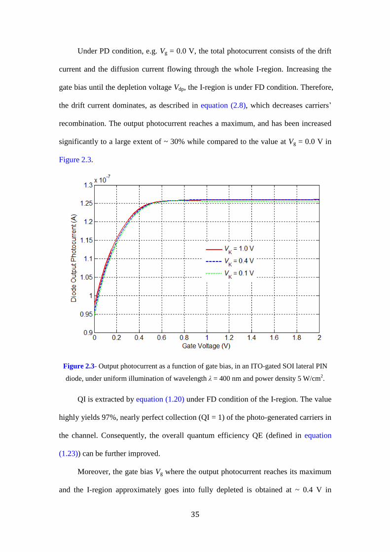
Under PD condition, e.g. Vg = 0.0 V, the total photocurrent consists of the drift
current and the diffusion current flowing through the whole I-region. Increasing the
gate bias until the depletion voltage Vdp, the I-region is under FD condition. Therefore,
the drift current dominates, as described in equation (2.8), which decreases carriers’
recombination. The output photocurrent reaches a maximum, and has been increased
significantly to a large extent of ~ 30% while compared to the value at Vg = 0.0 V in
Figure 2.3.
Figure 2.3- Output photocurrent as a function of gate bias, in an ITO-gated SOI lateral PIN
diode, under uniform illumination of wavelength λ = 400 nm and power density 5 W/cm2.
QI is extracted by equation (1.20) under FD condition of the I-region. The value
highly yields 97%, nearly perfect collection (QI = 1) of the photo-generated carriers in
the channel. Consequently, the overall quantum efficiency QE (defined in equation
(1.23)) can be further improved.
Moreover, the gate bias Vg where the output photocurrent reaches its maximum
and the I-region approximately goes into fully depleted is obtained at ~ 0.4 V in

36
Figure 2.3, well consistent with the depletion voltage Vdp = 0.434 V which is directly
calculated by equation (2.7) with specific values of the parameters implemented into
this simulation set-up.
Figure 2.4- Longitudinal holes and electrons concentrations in the I-region of the ITO-gated
thin-film SOI lateral PIN diode, in the dark.
Holes and electrons concentrations (cm-3
) are further probed in the dark to
mainly investigate the depletion condition modified by gate bias. They are probed
from the front surface of the active Si film to the back surface at the middle of the
intrinsic region, i.e. starting from a depth of 0.0 µm and ending at a position of 0.80
µm as in Figure 2.4, at reverse voltages VK of 0.0 V and 1.0 V. Increasing the reverse
bias VK from 0.0 to 1.0 V, the vertical depletion condition is almost not affected while

37
compared the data in each sub-figures of Figure 2.4. At Vg = 0.0 V, the intrinsic
region is partially depleted due to the positive fixed oxide charges and workfunction
difference between ITO and P-type doped silicon, with a vertical depletion width of ~
100 nm in Figure 2.4(a), which leads to an effective optical absorption of ~ (1-e-1
).
Increasing Vg to 0.2, 0.4 V, as depicted in Figure 2.4(b), (c), the intrinsic region is
fully depleted at 0.4 V, which leads to an effective optical absorption of (1-e-8
) ≈ 1.
These explain and validate the increment of ~ 30% in QI which is extracted in Figure
2.2, as gate bias increases from 0.0 V (i.e. PD condition) to 0.4 V (i.e. FD condition).
2.2.2.2 Intrinsic length variation
Considering the variation in the intrinsic length Li, besides Li = 8 µm, seven other
intrinsic lengths (Li = 1, 2, 4, 6, 10, 20 and 30 µm) [42] are investigated in this part.
Under uniform illumination of incident wavelength λ = 400 nm and optical power
density 5 W/cm2, QI extracted in the top ITO-gated SOI lateral PIN diodes for the
various intrinsic lengths (Li = 1, 2, 4, 6, 8, 10, 20 and 30 µm) is illustrated in Figure
2.5, at reverse biases VK = 1.0 and 2.0 V and under FD condition by gate bias. No
anti-reflection coating (ARC) or RCE is included.
For the short length (Li < 8 μm), QI exceeds 95% at λ = 400 nm, with no
discernible difference between at VK = 1.0 V and VK = 2.0 V-biased conditions. Under
FD condition, loss of the photo-generated carriers in the short length case can be
totally negligible at VK = 1.0 and 2.0 V due to high electric field, while the carriers
drift across the I-region.
For the long lengths (Li = 10, 20 and 30 μm), low-field mobility and carrier
diffusion length need to be taken into account. With the typical value of carrier
lifetime 0.1 µs and specified electron and hole's mobility of 1400 and 450 cm2 V
-1 s
-1,
the diffusion lengths Ldiff of electron and hole are calculated to be 18.974 μm and

38
1.077 μm, respectively. In this case, volume SRH recombination occurs in the region
exceeding the carrier diffusion length while carriers drift across the I-region. In the
meantime, there is certain surface recombination velocities (s.n = s.p = 104 cm/s) at
the front and back oxide interfaces which is often the dominant recombination
mechanism in SOI [43]. The device presents an increasing reduction in the maximum
photocurrent (i.e. QI) as Li increases, due to carriers' recombination in the I-region.
Especially while Li exceeds the diffusion length, there is a remarkable drop of QI due
to the volume SRH recombination. As observed in Figure 2.5, QI drops to 75% at VK
= 1.0 V and then yields about 87% at VK = 2.0 V for Li = 30 μm under FD condition,
with a slight increase of QI due to the strengthened reverse electrical field and
decreased recombination by reverse bias VK (from 1.0 V to 2.0 V).
Figure 2.5- QI extracted in ITO-gated SOI lateral PIN diodes with different intrinsic lengths
(Li = 1, 2, 4, 6, 8, 10, 20 and 30 μm), under λ = 400 nm illumination, at VK = 1.0 V, 2.0 V and
under FD condition.
Furthermore, a high ratio of more than 107 between illuminated to dark currents
discussed in Chapter 2.2.1 is achieved, under FD condition and the low-voltage

39
operation, based on the diode output photocurrent and dark current with Li = 1, 2, 4, 6,
8, 10, 20 and 30 µm.
2.2.2.3 Doping concentration variation
In optical sensors (e.g. the ITO-gated SOI lateral PIN photodiode) fabricated in
different SOI materials such as UNIBOND, SIMOX, ZMR, the I-region practically
corresponds to various P-doping levels [34]. This section investigates the gate effect
on the ultimate device optical performances, with the variation in the P-doping
concentration.
Based on the device schematic diagram depicted in Figure 2.1 and the
corresponding settings in device geometry (Li, Ln, Lp, dox1, dox2, dSi), electrical (carriers’
lifetime τ, SRV (s.n, s.p) and Qox) and optical (e.g. R0 = 0) implementations, six
different P-doping concentrations in the I-region: 6×10¹⁴
, 8×10¹⁴
, 1×10¹⁵
, 2×10¹⁵
,
5×10¹⁵
and 1×10¹⁶
cm-3
[41]. are considered and further simulated into
Atlas/SILVACO. Doping concentrations in the N+ and P
+ regions are fixed to 10
20
cm-3
.
The SOI lateral PIN diodes with ITO top gate and without gate are discussed in
this part, for the comparison. Gate application is supposed to optimize the device
optical response (i.e. QI). The extracted QI (by equation (1.20), i.e. the ratio of the
device output photocurrent over the available photocurrent) under varied doping
concentration is illustrated in Figure 2.6, for the SOI photodiodes with and without
gate.
QI in the gated photodiode always yields in excess of 90%, even approximately
100%, as the doping concentration increases from 6×10¹⁴
cm-3
to 1×10¹⁶
cm-3
. In
contrast, QI in the ungated diode decreases sharply from > 95% at doping of 6×10¹⁴

40
cm-3
to merely ~ 40% for doping of 1×10¹⁶
cm-3
, with a slight increase introduced by
VK from 1.0 to 2.0 V in Figure 2.6.
The I-region in the gated PIN photodiode can be fully depleted (FD) by the
positive gate bias (as discussed in Chapter 2.2.1.1) applied to the ITO transparent
electrode, carriers’ recombination (outside of the reverse depletion region Lzd) is
therefore reduced and all the charges are efficiently collected. Whereas the I-region
(with Li = 8 µm) of the photodiode without gate is under partially depleted condition
(i.e. the depleted region is laterally caused by the reverse bias VK), SRH
recombination (outside of the diffusion length) significantly increases with the doping
concentration, leading to the QI decrease in Figure 2.6.
Figure 2.6- Extracted QI in the SOI lateral PIN photodiodes with and without gate, at VK =
1.0 and 2.0 V, for P-doping levels of 6×10¹⁴
, 8×10¹⁴
, 1×10¹⁵
, 2×10¹⁵
, 5×10¹⁵
and 1×10¹⁶
cm-3
,
with incident λ = 400 nm and power density 5 W/cm2.

41
Consequently, the top transparent gate applied to SOI lateral PIN diode has
optimized the device performance under varied doping concentration, i.e. achieving
QI close to 100%, due to the FD condition caused by gate bias.
2.2.2.4 Varied incident wavelength
Keeping the P-doping concentration of the I-region at 1×10¹⁵
cm-3
and the intrinsic
length 8 µm, optical response of the ITO-gated SOI lateral PIN photodiode
illuminated with different incident wavelengths (280, 350, 400, 450, 530 and 600 nm)
are discussed [44], in this part. The corresponding thickness of the active silicon film
(dSi) is 0.4 µm for 280 nm and 350 nm wavelengths, 1.0 µm for 400 nm and 450 nm
wavelengths, and 2.5 µm for 530 nm and 600 nm wavelengths, respectively,
considering with the light penetration depth in Si (in Figure 1.5).
Figure 2.7- Internal quantum efficiency (QI) versus wavelength for the top ITO-gated SOI
lateral PIN photodiode under fully depleted condition, at VK = 1.0 V and 2.0 V, with incident λ
= 400 nm and power density 5 W/cm2.

42
Internal quantum efficiency (QI) versus wavelength for the top ITO-gated SOI
lateral PIN photodiode is extracted under FD condition and at reverse biases of 1.0
and 2.0 V, as presented in Figure 2.7. Under monochromatic illumination of relatively
long wavelengths (400, 450, 530 and 600 nm), QI yields over 96% at FD condition.
For short wavelengths 280 and 350 nm, QI is decreased to approximately 70% and
80% respectively, due to the carriers’ recombination (with SRV 104 cm/s) at the
surface where the photo-generated carriers are mainly created.
Generally, the gate bias applied to the ITO top transparent electrode can achieve
the FD condition in the I-region of the thin-film SOI lateral PIN diode, therefore
maximize the diode output photocurrent and corresponding QI, under different
incident wavelength, with varied intrinsic length, doping concentration, etc.
2.3 An experimental Al-gated SOI lateral PIN
diode
2.3.1 Device geometry
An experimental device available for a first study (before a graphene transparent gate
can be fabricated and studied in Chapter 5) is investigated with a back aluminum
(Al) -gate control.
Schematic view of a SOI lateral PIN diode with Al back gate is depicted in
Figure 2.8, showing a notably 300 nm-thick polysilicon layer, a 250 nm-thick active
silicon film and a 1 µm-thick buried oxide layer. The PIN diode is suspended on a
micro-hotplate platform and the 1 µm-thick aluminum layer is deposited on device
backside by electron-beam (E-beam) evaporation (The process will be described in
details in Chapter 3). Full two-dimensional (2-D) numerical simulations are
conducted in Atlas software from SILVACO Int. (Atlas/SILVACO) [40], on a

43
physical device model with intrinsic length Li = 10 µm. Length of the P+ and N
+
regions is 2.5 µm. The intrinsic (P-), P
+ and N
+ doping levels are about 510
15, 110
20,
11020
cm-3
, respectively. The polysilicon is treated as an insulator in the electrical
simulations, as it is left electrically unconnected in the device fabrication. Ohmic
contacts are implemented onto the anode and cathode electrodes, and the back gate
electrode is specified for an Al workfunction of 4.10 eV. No fixed oxide charge, nor
interface trap, is specified.
Figure 2.8- Schematic view of a SOI lateral PIN diode with aluminum back gate: FD1 =
region depleted by reverse anode bias, FD2 = region depleted by back-gate voltage, NFD =
undepleted part.
2.3.2 Depletion regime with back gate bias
Depending on the back gate VG and anode VD biases, the I-region features an
undepleted zone (NFD) and two main depletion zones, one arising from P–N
+ junction
(FD1), one from BOX interface (FD2) (in Figure 2.8) [45].
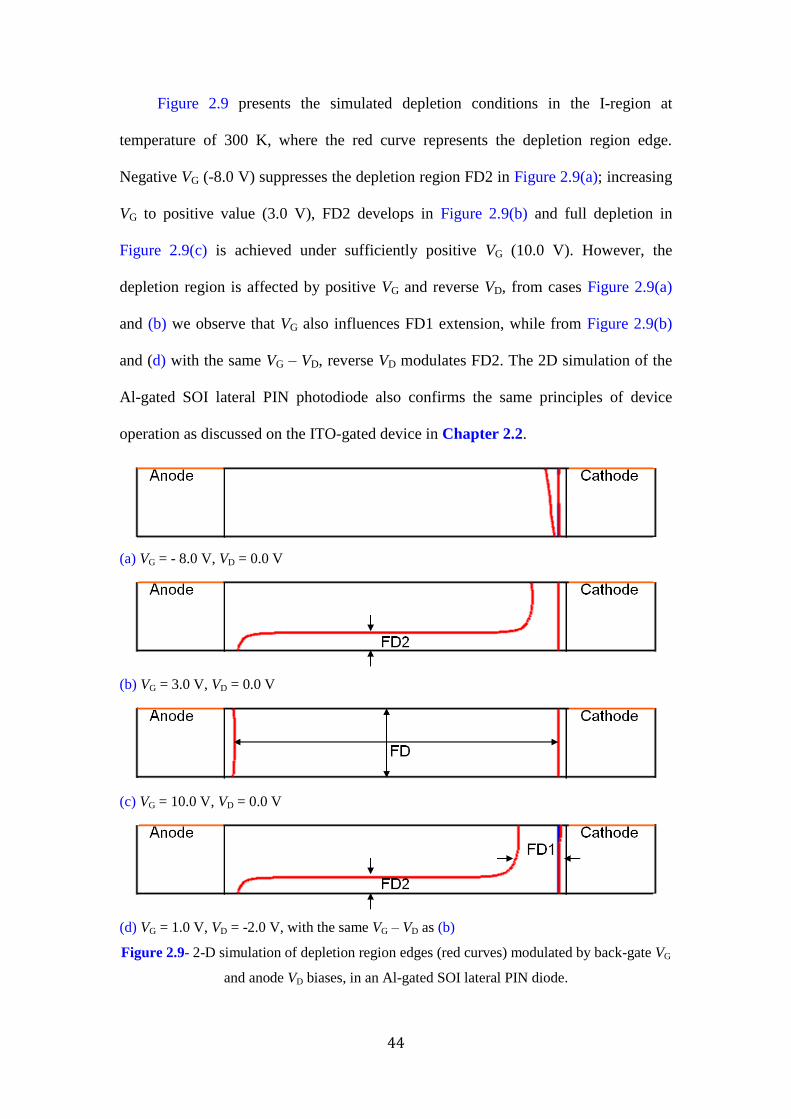
44
Figure 2.9 presents the simulated depletion conditions in the I-region at
temperature of 300 K, where the red curve represents the depletion region edge.
Negative VG (-8.0 V) suppresses the depletion region FD2 in Figure 2.9(a); increasing
VG to positive value (3.0 V), FD2 develops in Figure 2.9(b) and full depletion in
Figure 2.9(c) is achieved under sufficiently positive VG (10.0 V). However, the
depletion region is affected by positive VG and reverse VD, from cases Figure 2.9(a)
and (b) we observe that VG also influences FD1 extension, while from Figure 2.9(b)
and (d) with the same VG – VD, reverse VD modulates FD2. The 2D simulation of the
Al-gated SOI lateral PIN photodiode also confirms the same principles of device
operation as discussed on the ITO-gated device in Chapter 2.2.
(a) VG = - 8.0 V, VD = 0.0 V
(b) VG = 3.0 V, VD = 0.0 V
(c) VG = 10.0 V, VD = 0.0 V
(d) VG = 1.0 V, VD = -2.0 V, with the same VG – VD as (b)
Figure 2.9- 2-D simulation of depletion region edges (red curves) modulated by back-gate VG
and anode VD biases, in an Al-gated SOI lateral PIN diode.

45
2.3.3 Experimental characterization
Experimental characterization, with the back gate control, is done in the device
samples with three different intrinsic lengths Li = 5, 10 and 20 µm. More details will
be presented in Chapter 3, but not necessary here for this aim.
Device chips are mounted in a dual-in-line (DIL) 16 ceramic package and
embedded in a printed circuit board (PCB) for the measurements. Muller LXH 100
light source and a monochromator are used to select single wavelength λ illumination
within the wavelength range 200-1600 nm with bandwidth of ~ 10 nm and light
power density on the level of 10-6
-10-4
W/cm2. (It will be used in the measurements of
Chapter 4 and Chapter 5). For the electrical measurements, semiconductor
parameter analyzer (Agilent, HP4156) and low leakage switch mainframe (Agilent,
E5250A) are used to obtain the current-voltage curves at room temperature (RT), as
depicted in Figure 2.10.
Figure 2.10- Measurement set-up for experimental characterization at room temperature.

46
2.3.3.1 Fully-depleted condition by back-gate bias
Figure 2.11- Normalized photocurrent as a function of back-gate voltage, in Al-gated SOI
lateral PIN photodiodes (with Li = 5, 10 and 20 µm), with 590 nm illumination (at 8.9210-5
W/cm2) and under different reverse anode biases VD.
Figure 2.11 presents the measured photocurrents under 590 nm incident light, in the
one-finger suspended photodiodes M5, M10 and M20 respectively with the device Li
= 5, 10 and 20 µm, as a function of the applied back-gate voltage (VG) and at different
reverse anode bias (VD). The variation of VG modifies the operation mode of the active
silicon film back interface, from accumulation to depletion and inversion for negative
to positive bias, leading to fully-depleted (FD) condition in the I-region. It is clearly
seen that, to the first order, the photocurrents are modulated by the back gate bias VG,
i.e. the vertical depletion width WD (which is roughly with the square root of positive
VG above flat band voltage VFB and back surface potential Ψs [2]). In this case,
. The output photocurrents achieve a maximum under FD

47
condition whose value is directly proportional to Li as is expected from carrier
collection over the full I-region volume. The shift of the photocurrent characteristics
among the different diodes is related to fixed oxide charge Qox, which will be
discussed in Chapter 3.
2.3.3.2 Non-fully-depleted (NFD) regime
Figure 2.12- Photocurrent for single-finger diode as a function of reverse anode voltage,
under non-fully-depleted operation at proper back-gate bias VG.
The diode photocurrents also vary with reverse anode bias (VD), but only in the non-
fully-depleted (NFD) intermediate regime. In this case, Figure 2.12 shows that at
constant VG – VD (to avoid modulating the vertical depletion width from back
interface with VD), the photocurrent indeed increases with the lateral depletion width
Lzd (as indicated by black dashed curve in Figure 2.12) at the P–N
+ blocked junction,
which is roughly following the square root of Vbi – VD (i.e. ) where
Vbi is the built-in contact potential [8]. This cannot occur anymore, once fully-

48
depleted (FD) condition is achieved by increasing VG (Figure 2.11) or when very
negative VG (e.g. at -12.0 V for diode with Li = 20 µm, -20.0 V for diodes with Li = 5
and 10 µm in Figure 2.11) impedes carrier collection. Furthermore, it confirms the
first-order interpretation of depletion regime in the simulations depicted in Figure 2.9.
Similar behaviors, i.e. current-voltage characteristics with back-gate and reverse
anode voltages, are observed at all wavelengths in the visible spectrum.
2.4 Summary
In this chapter, a SOI lateral PIN diode with ITO transparent gate is fully investigated,
with device performance simulated in a 2-D Atlas/SILVACO device model. Gate
voltage is applied to modulate the depletion condition in the I-region. Under FD
condition achieved by the gate bias, carriers drift across the whole I-region with
negligible carriers’ recombination, the photodiode achieves the optimized optical
response, i.e. the maximized output photocurrent and QI under different doping
concentration, intrinsic length and incident wavelength. A maximized intrinsic length
of 20 µm is obtained while considering the carrier diffusion length in the 2-D
simulation, where the optimized QI of the lateral PIN photodiode under FD condition
keeps close to 1. This could guide the device design in technology.
A second Al-gated SOI lateral PIN diode, with the 1 µm-thick Al layer
deposited on the backside, has been characterized and experimentally validates the
electrical performance optimized by the gate bias control. Photodiode output
photocurrents indeed reach a maximum under the FD condition achieved by the
positive voltage applied to the Al back gate.
However, the observed variation in the device experimental characterizations,
e.g. shift in the current-voltage curves, which may be related to the fixed oxide
charges and the electrical conditions inside diode will be discussed in Chapter 3, with
49
regards to the MEMS processing. The improvement and optimization of the device
optical response based on the available device sample and structure will be
investigated in Chapter 4.

50
CHAPTER 3
Device degradation and local
annealing
In the CMOS technology and device fabrication process, defects or charges are
unavoidably induced. For example, fixed oxide charges are related to the oxidation
process, interface states or traps [46] located at the SiO2/Si interfaces are due to the
non-periodic crystal structure of the Si surface, mismatch between Si and SiO2 lattices,
oxidation process or other similar bonding breaking process (e.g. plasma ion etch)
[47]. Hence a final low-temperature (~ 450 °C) hydrogen or forming gas annealing is
often used at wafer level to reduce the density of the interface traps, which plays an
important role in device behavior [48].
In this chapter, device (SOI lateral PIN diode) degradation induced by the
MEMS post-processing (i.e. deep reactive ion etching (DRIE) and aluminum backside
deposition), with regards to the diode forward and reverse characteristics will be
discussed. The DRIE is performed at wafer level, thereafter a forming gas annealing
can follow before dicing. The Al backside deposition is done at die level in our case,
where a local annealing is necessary and needed to recover the device degradation
which is induced by the Al deposition or may occur during operation at package level
(e.g. due to radiation). A local annealing is thereafter performed on the basis of the
available micro-heater, with temperature-control using the PIN diode as temperature

51
sensor, for the device recovery and performance improvement. 2-D simulations are
further performed in Atlas/SILVACO to analyze the leakage behavior in the SOI
lateral PIN diode and therefore identify the generation mechanism, with specific
implementations of surface recombination velocity, carriers’ lifetime, interface traps
or defects, etc.
3.1 Device fabrication and operation
3.1.1 Micro-hotplate platform and MEMS post-processing
A three dimensional (3-D) schematic of lateral PIN diodes lying on the suspended
micro-hotplate platform and on the standard Si substrate is depicted in Figure 3.1.
Table I lists the superposed materials and their process targeted thicknesses. The
lateral PIN diode and the micro-heater are embedded in a thick SiO2 membrane (~ 5
µm), released by a post-CMOS DRIE of the substrate at wafer level, where the 1 µm-
thick buried oxide acts as an effective etch-stop layer, ensuring membrane high
uniformity and, as a result, excellent device reproducibility. Aluminum metallization
is used to contact the diode anode and cathode terminals and build the micro-heater,
because of its low cost and industrial technology availability.
The micro-hotplate membrane has a circular shape to minimize stress effect and
enhance the mechanical robustness. The thickness is ~5 µm with membrane diameter
of 600 µm and heated area diameter of 100 µm, respectively. The typical power
consumption of fabricated micro-hotplates is 35 mW for heating at 600 °C [49], i.e.
very high efficiency of ~ 15 °C/mW.
An additional 1 µm-thick aluminum (Al) layer is specifically deposited on the
device backside by electron-beam (E-beam) evaporation (with a deposition rate 0.1-
1.0 nm/second) at Université catholique de Louvain, WINFAB clean room (i.e.

52
VACOTEC e-beam evaporation system), at die level. The E-beam evaporation is a
physical vapor deposition (PVD) technique whereby an intense, electron beam is
generated from a filament and steered via electric and magnetic fields to strike source
material (e.g. pellets of aluminum) and vaporize it within a vacuum environment [50]
[51].
Figure 3.1- Three dimension (3-D) schematic (not to scale) of the SOI micro-hotplate multi-
sensor technology platform, a lateral PIN diode lying on the membrane surrounded by a
micro-heater and a PIN diode lying on the substrate.
TABLE I
MATERIALS AND THICKNESSES LIST
Function Material Thickness Color
Passivation Si3N4 PECVD* 550 nm
Grey
Membrane SiO2 PECVD* 2.5 µm Light blue
Heater Aluminum
500 nm Orange
Implantation protection Polysilicon 300 nm Green
Gate dielectric SiO2 25 nm Light blue
Active thin film Silicon 250 nm Dark blue
Buried oxide layer (BOX) SiO2 1 µm Light blue
Substrate Silicon 375 µm Dark blue
*The film was deposited by plasma-enhanced chemical vapor deposition (PECVD) technology.

53
Cross section of the SOI lateral PIN diodes on membrane and on substrate with
Al deposited on the device sample backside is presented in Figure 3.2, where the
bottom orange layer represents the additional 1 µm-thick Al layer. Electrically, back
gate voltage can be applied to the Al layer, modifying the operation mode of the
intrinsic (P-) region (which has been used in Chapter 2.3 for the first experimental
characterization of the back Al-gated SOI lateral PIN diode); optically, the Al layer
can be used as a backside reflector, to modulate light reflection and absorption back
into the device active Si film (which will be discussed in details in Chapter 4).
Figure 3.2- Cross-section view of the SOI lateral PIN diodes on membrane (a) (i.e. micro-
hotplate platform) and on substrate (b) after Al deposition: Si3N4 passivation (grey), SiO2
dielectric (light blue), silicon (dark blue), polysilicon (green), aluminum contacts, micro-
heater and deposition layer (orange).
3.1.2 Available SOI lateral PIN (P+/P–/N+) diodes
The device sensor consists of a number of P+/P
–/N
+ (PIN) finger diodes interdigitated
in parallel over a given sensing area (~ 60 µm 60 µm). The PIN diode design lies in
a trade-off concerning the size of the intrinsic length (Li), i.e. the lateral distance
between P+ and N
+ regions. Given that the P
+ and N
+ sizes are fixed by technological

54
constraints on the minimum contact areas, using a longer Li can enhance optical
sensitivity thanks to a larger photogeneration area for a given full photodiode area if
used for optical sensing, while smaller Li can enhance electrical response (i.e. on/off
current ratio) [52].
Figure 3.3- Chip top views with 3 different intrinsic lengths (5/10/20 µm) and 2 different
locations: M-series = on-membrane with a surrounding micro-heater and S-series = on-
substrate.
Figure 3.3 presents the SOI micro-hotplate devices on a 1.8 mm 1.8 mm chip,
which contains 6 PIN detectors. The so-called devices S5, S10, and S20 are on

55
substrate with the geometries as specified in Table II. The devices M5, M10 and M20
have identical geometries but are suspended on the membrane and surrounded by a
circular heater. Three different intrinsic lengths are implemented: 5, 10, and 20 µm,
with the number of fingers 6, 4, and 2, respectively. The lengths of P+ and N
+ regions
(i.e. Lp, Ln) are 4 µm, limiting the effective area (A) to total area (Atot) ratio. The width
of each device (Wfingers) is 60 µm.
TABLE II
DEVICE GEOMETRIES
Devices Li
(µm) Fingers
Wfingers
(µm)
Effective area A
(µm µm)
Total area Atot
(µm µm)
M5, S5 5 6 60 30 60 58 60
M10, S10 10 4 60 40 60 60 60
M20, S20 20 2 60 40 60 52 60
3.1.3 Local annealing operation
Usually, a furnace tube is dedicated to annealing silicon wafer in forming gas ambient
(e.g. a gas mixture of hydrogen (90%) and nitrogen (10%)), at high temperature
between 400 and 700 °C for 30 minutes, i.e. a standard high-temperature forming gas
annealing [53] [54]. Instead of the standard forming gas annealing, we consider a low-
temperature annealing in this thesis, based on the available micro-heater and the PIN
diode, to optimize and stabilize the device performance and characteristics at die or
package level.
The micro-heater on the suspended micro-hotplate platform is designed to be
used as a heat source to increase the local temperature. The on-membrane diode can
be heated beyond 300 °C with low-power consumption and long-term stability [11],
thanks to excellent thermal insulation from the heat dissipating substrate and device
package

56
The diode itself can be used as a standard temperature sensor, it was firstly
described in equations (1.15) and (1.18): while driven by a constant forward current IF,
the diode forward voltage VF decreases linearly with the increasing temperature T, as
given in equation (3.1) [55]:
(3.1)
where d is the temperature linear coefficient of the diode. By first calibrating the
device voltage-temperature (VF-T) characteristics, e.g. on a reference heated chuck at
die level or in an oven at package level, in-situ temperature sensing and control can
next be achieved with the micro-heater and the suspended PIN diode.
Using a heated and temperature-controlled wafer chuck, the forward voltage
versus temperature (VF-T) measurement of the on-membrane (M10) and on-substrate
(S10) diodes is performed from RT up to 300 °C. The VF-T plot for the on-membrane
device M10 is shown in Figure 3.4, the solid line obtained under high-power blue
LED illumination, the dashed line without illumination. Up to more than 200 °C, there
is no significant difference of the diode forward voltages between the illuminated and
non-illuminated conditions, and good linearity for the thermal sensing has been
achieved under different drive currents (1, 5, 10, 50 and 100 µA). The VF-T plot for
the photodiodes M10 and S10 with illumination is presented in the inset to Figure 3.4
with the good reliability and stability of the on-membrane diode fabricated by the
MEMS post-processing DRIE. However, the temperature linear coefficient varies,
depending on the specific device and the fabrication technology.
Consequently, while heating device with the micro-heater and referencing these
VF-T curves (e.g. in Figure 3.4), in-situ temperature sensing and accurate temperature
control for the on-membrane diode can be achieved. Therefore, the local annealing is
directly carried out onto the suspended SOI lateral PIN diode, during a 30-minute

57
heating by the surrounding micro-heater (power consumption ~ 60 mW) at elevated
temperature ~ 250 °C, in order to neutralize additional traps and charges which were
introduced by the MEMS post-processing, so as to finally stabilize and optimize
device performance under reverse and forward conditions.
Figure 3.4- Forward voltage drop versus temperature of the on-membrane diode (M10) for
different drive currents IF (1/5/10/50/100 µA), from room temperature (RT) to 300 °C. The
inset shows the comparison of forward voltage drop between M10 and S10, under
illumination.
3.2 Process-induced degradation and local-
annealing improvement
3.2.1 Diode forward characteristics
Physically, the diode forward current IF in the dark is theoretically related to the sum
of diffusion and generation-recombination (G-R) currents, as given below [7]:

58
(3.2)
(3.3)
(3.4)
(3.5)
(3.6)
where I0
GR is the diode G-R saturation current which relates to the intrinsic carrier
density ni, I0 is the diode diffusion current which is dependent on ni2, as firstly
described in equation (1.15). Thermal voltage kT/q is 25.8 mV at room temperature of
27 °C. In silicon, under standard temperature (T < 150 °C) IF is dominated by the G-R
current at low forward bias (e.g. VF < 0.4 V) and then by the diffusion current as
voltage increases, as typically presented in the curves of Figure 3.5. These correspond
to the forward current versus voltage (IF-V) characteristics in the standard on-substrate
diodes S5, S10 and S20 (with Li = 5, 10 and 20 µm), with temperature variation from
50 °C to 200 °C.
The ideality factor η in equation (3.4) depends on the diode technology and the
device operation regime, and finally affects the temperature linear coefficient d
described in equation (3.1). Diode ideality factor η close to 1 indicates the dominance
of the diffusion current, while ~ 2 indicates the dominance of the G-R mechanism.
For example, at temperature of 50 °C, the G-R current is dominant in the diodes
S5/S10/S20 at forward bias range 0.1-0.3 V, then diffusion current becomes dominant
with the increased forward bias 0.5-0.7 V in Figure 3.5. While temperature T
increases from 50 °C to 150 °C, the diffusion current I0 increases with ni2 and

59
becomes larger than I0
GR, and dominating in a wider VF range for the diode forward
current IF.
Experimentally, the PIN diode is used for the thermal sensing mainly in the
linear region where the diffusion current or the G-R current keeps its dominance as
temperature increases. For example, a diode forward current in the range of 0.01-1 µA
in Figure 3.5, where the diffusion current keeps its dominance as the temperature
increases from 50 °C to 150 °C, can be chosen as the drive current for the thermal
sensing application.
In the forward condition, as in Chapter 1.2.2, the diffusion current is
independent of diode intrinsic length Li. The diodes S5, S10 and S20 in Figure 3.5
present the same forward current values when diffusion is dominant in the range of
0.01-1 µA. However, the G-R current (e.g. at VF < 0.2 V) is related to Li due to the
electric field as described in equation (1.14). The diodes S20, S5 with Li = 20, 5 µm
respectively present the highest and lowest values of forward current, while IF is low,
< 10-10
A and with the dominance of the G-R current, due to the corresponding lowest
and highest values of electrical field at the same forward bias.

60
Figure 3.5- Diode forward current versus anode voltage (IF-V) in the reference on-substrate
diodes S5/S10/S20 (with Li = 5, 10 and 20 µm), at temperature T of 50, 100, 150 and 200 °C.
3.2.1.1 After DRIE
Forward current versus voltage (IF-V) characteristics of the suspended SOI lateral PIN
diodes M5/M10/M20 (with Li = 5, 10 and 20 µm) are representatively presented in
Figure 3.6, after the MEMS post-processing DRIE to fabricate the micro-hotplate
platform (in Figure 3.1) without annealing. In comparison with the forward
characteristics in the reference diodes S5/S10/S20 (Figure 3.5), obvious device
degradation is observed in Figure 3.6 in the diodes after the DRIE. Diode ideality
factor η of the suspended PIN diodes M5/M10/M20 is close to 2 under the whole
forward-biased condition, indicating the G-R current dominance in the whole forward
range.

61
Figure 3.6- Diode forward current versus anode voltage (IF-V) in the suspended SOI lateral
PIN diodes M5/M10/M20 (with Li = 5, 10 and 20 µm), after DRIE and without annealing, at
temperature T of 50, 100, 150 and 200 °C.
Device instability is also observed after the post-processing DRIE, based on the
variation in the forward IF-V characteristics of the single diodes M5/M10/M20
presented in Figure 3.6. Moreover, the forward current in the diode M20 (IF(M20)) is
always higher than that in the diode M5 (IF(M5)), which validates the G-R current
(relevant to Li) dominance in the whole forward range.
A low-temperature local annealing is then performed on the suspended SOI
lateral PIN diode M10, i.e. a 30-minute local heating by the micro-heater at estimated
temperature of 250 °C. Figure 3.7 presents the forward IF-V characteristics of the
diode M10, in temperature range from 50 °C to 200 °C. Red curves indicate the diode
forward IF-V after the first-cycle annealing and blue curves represent the second-cycle
annealing.

62
The forward performance of the diode M10 has been largely improved or
recovered after the first annealing, i.e. the right shift from the green curves (without
annealing) to the red curves (after a first annealing) in Figure 3.7. Moreover, at
temperature of 50 °C, the G-R dominance is present at low forward bias (~ 0.1-0.2 V)
and then the diffusion current dominates as bias increases only in the diode M10 after
annealing. Slight improvement from the second-cycle annealing indicates that one
cycle of annealing for the suspended diode is sufficient.
Improvement of the thermal linearity is further achieved in the diode after
annealing, with the corresponding temperature linear coefficient d (e.g. at diode
forward current of 1 µA) described in equation (3.1).
Figure 3.7- Diode forward current versus anode voltage (IF-V) in the suspended SOI lateral
PIN diode M10, after two cycles of annealing (the first-cycle annealing in red, the second-
cycle annealing in blue), at temperature T of 50, 100, 150 and 200 °C.

63
3.2.1.2 With Al deposition and back gate influence
The backside aluminum (Al) deposition process also affects the diode forward
performance. Figure 3.8 representatively presents the forward IF-V characteristics of a
suspended diode M10 before Al and after Al deposition without annealing, where gate
bias is 0 V. A second device degradation induced by the Al deposition process is
observed, where the diode forward IF-V curves in Figure 3.8 are highly shifted to the
left from the dashed lines (before Al deposition) to the solid lines (after Al deposition,
without annealing). For example, the G-R current at a low bias of 0.1 V has been
increased by a factor of 102 in the diode M10 after Al and without annealing.
Furthermore, the thermal linearity between the diode forward voltage and the
temperature cannot be found under a constant drive current.
Figure 3.8- Diode forward current versus voltage (IF-V) in the suspended SOI lateral PIN
diode M10, before and after Al deposition without annealing (with gate bias 0 V), from room
temperature to 200 °C.

64
After local annealing at 250 °C for 30 minutes, in Figure 3.9 we see again the
recovery of the diode forward performance (especially the diffusion current, but the
G-R current is still a bit higher) in reference with the diode M10 before Al deposition,
where gate bias in the suspended diode M10 with Al is 0 V.
Furthermore, based on the available back gate (i.e. the backside Al layer), we
consider the influence of back gate bias on the diode forward characteristics in Figure
3.10. At gate bias of 90 V, fully-depleted (FD) condition can be achieved in the I-
region of the suspended diode where the 1 µm-thick buried oxide (BOX) layer is used
as the gate dielectric. It is clearly seen that there are two dominant mechanisms (i.e.
the G-R current dominance and the diffusion current dominance) seen in the diode
M10 forward characteristics, similar to the forward characteristics of the standard
diode S10 in Figure 3.5.
Figure 3.9- Diode forward current versus voltage (IF-V) in the suspended SOI lateral PIN
diode M10, after annealing (with gate bias 0 V), from room temperature to 200 °C.
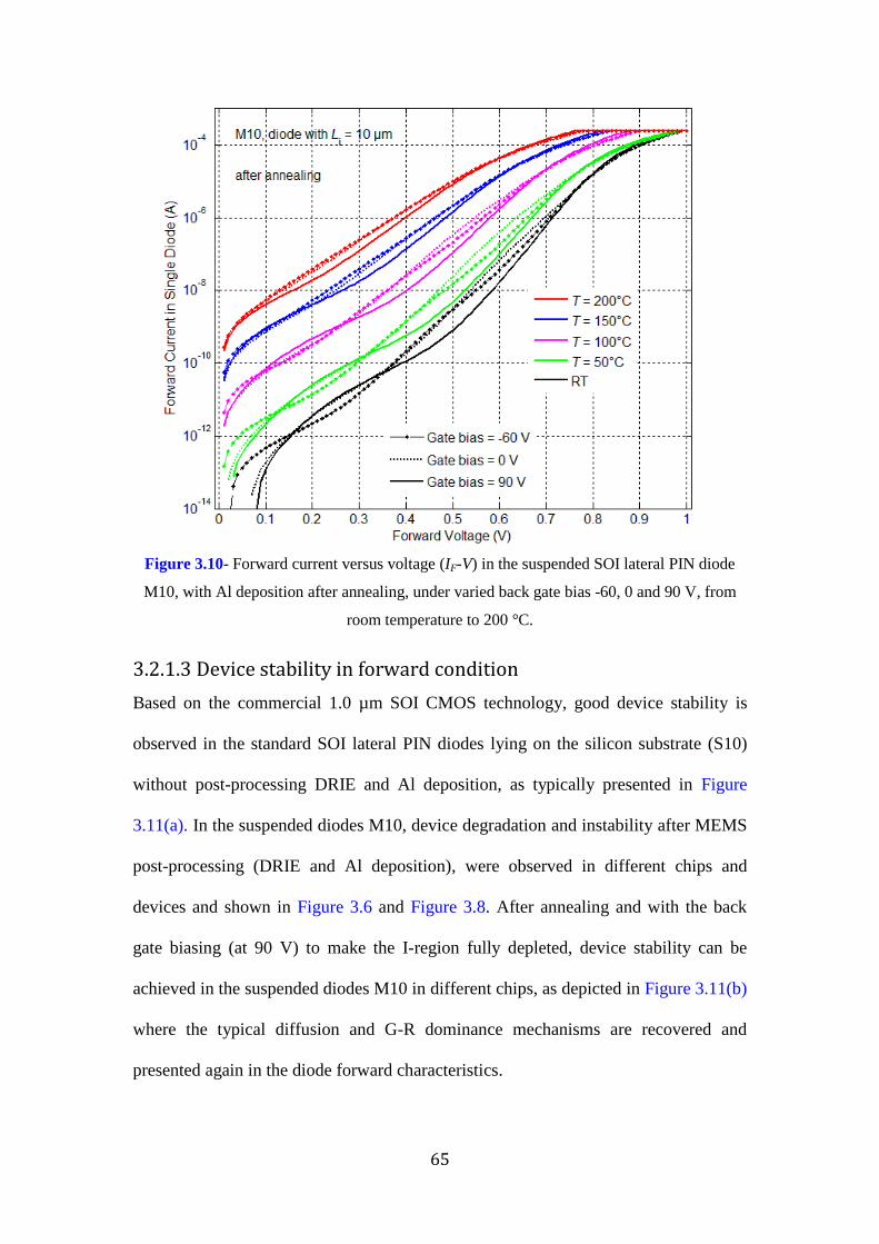
65
Figure 3.10- Forward current versus voltage (IF-V) in the suspended SOI lateral PIN diode
M10, with Al deposition after annealing, under varied back gate bias -60, 0 and 90 V, from
room temperature to 200 °C.
3.2.1.3 Device stability in forward condition
Based on the commercial 1.0 µm SOI CMOS technology, good device stability is
observed in the standard SOI lateral PIN diodes lying on the silicon substrate (S10)
without post-processing DRIE and Al deposition, as typically presented in Figure
3.11(a). In the suspended diodes M10, device degradation and instability after MEMS
post-processing (DRIE and Al deposition), were observed in different chips and
devices and shown in Figure 3.6 and Figure 3.8. After annealing and with the back
gate biasing (at 90 V) to make the I-region fully depleted, device stability can be
achieved in the suspended diodes M10 in different chips, as depicted in Figure 3.11(b)
where the typical diffusion and G-R dominance mechanisms are recovered and
presented again in the diode forward characteristics.

66
With respect to the device reliability, stability and the industrial feasibility yield,
the local annealing needs to be taken into account before the device practical
applications.
3.2.2 Reverse leakage current
While using the SOI lateral PIN diode as an optical sensor, in addition to large optical
response, low leakage current and low noise [56] [57] [58] are desirable to improve
the minimum detectable signal, the optical dynamic range and the reliability for these
optical sensing applications. The diode reverse leakage current, low-frequency noise
characteristics and carriers’ parameters will be discussed in details next, considering
the MEMS post-processing and the local annealing. Moreover in order to reduce this
leakage current, it is also important to understand the origin of the degradation
induced by the MEMS post processing, to identify the generation mechanisms in
device leakage behavior [59], to propose solutions to optimize device performance
[60].

67
Figure 3.11- Diode stability in forward characteristics of the reference SOI lateral PIN diodes
S10, with gate bias 0 V (a); Diode stability in forward characteristics of the suspended SOI
lateral PIN diodes M10, after annealing and with gate bias 90 V (b).

68
3.2.2.1 Without gate bias
Figure 3.12 presents the leakage currents in single diodes S10 and M10, at a reverse
bias 2.0 V and without gate bias, where temperature varies from RT to 200 °C. With
the operation temperature increasing (< 150 °C), the leakage current is dominated by
the generation current (as described in equation (1.17)), i.e. the volume SRH G-R
process. In comparison with the leakage currents of the diodes S10 (the black curves)
which is without the MEMS post-processing, the leakage currents in the diodes M10
after DRIE (the red curves) and the Al deposition (the green curves) without
annealing are increased, e.g. over 10-times increase. Furthermore, leakage current
variation is observed, which could result from different electrical conditions of the I-
region in the diodes M10 after the post-processing.
Figure 3.12- Reverse leakage current versus temperature in single diodes S10 and M10
without annealing, at reverse bias 2.0 V, without gate biasing.
On one hand, it is worth noting that the leakage current variation among the S10
diode without DRIE, the M10 diode (i.e. with DRIE) without Al, and the M10 diode
with Al deposition could also partly result from the electrical resistance of silicon with

69
respect to strain [61] [62] which was unavoidably induced by the MEMS processing
(i.e. DRIE and Al deposition). As described in [61], resistivity, length and its
transverse width can be changed while the silicon material is strained. Moreover,
mobility enhancement is also observed in the strained silicon, representative electron
and hole mobility enhancements of 100% and 50% were respectively measured in
fully depleted strained Si [63]. However, this enhancement can hardly explain the
orders of magnitude increase of leakage. Strain effect on the silicon devices or the
substrate thinned dies in Chapter 5 is then highly beyond the slope of this thesis, and
will not be investigated or discussed further.
3.2.2.2 Under gate biasing
Considering the influence of back gate bias, at RT, Figure 3.13 presents the typical
leakage currents of the SOI lateral PIN diodes after the Al deposition under a reverse
bias of 2.0 V and a back gate bias VB from -60 to 100 V [60]. Upon increasing gate
bias, the space-charge (SC) condition in the thin-film I-region at Si/BOX interface is
changed from accumulation (sc-a), to partial depletion (sc-b), full depletion (sc-c),
weak inversion (sc-d) and finally strong inversion (sc-e) in diode M10. As a result, the
corresponding leakage current increases from less than 10-12
A under accumulation,
reaches the maximum of 10-11
A under depletion conditions and returns to the level of
10-12
A when the I-region at Si/BOX interface goes into inversion (as will be clarified
through the physical simulations in Chapter 3.3.2).
After the low-temperature annealing performed in the air, the diode M10
leakage current is reduced by about one order of magnitude, i.e. from 10-12
-10-11
A
(before annealing) to 10-13
-10-12
A (after annealing). However, the leakage current in
the reference S10 diode is mainly on the order of 10-14
-10-13
A. Shape of the leakage
current versus VB curve (and SC conditions) is also different for this reference S10

70
diode as it is lying on the ~375 µm-thick Si substrate which is reversely driven from
inversion to depletion and accumulation changing the back gate coupling. The leakage
current characteristics obtained in the S10 diode experimentally validates the dark
current simulated in the ITO-gated lateral PIN diode (in Figure 2.6) where the top gate
bias varies from 0 to 1.0 V (with a top 30 nm-thick dioxide as gate dielectric) and
alters the I-region from accumulation to depletion conditions.
It is important to note that depending on SC conditions at Si/BOX interface,
related to exact back gate bias and oxide charge density, the leakage current
difference between S10 and M10 devices before annealing vary from 1 to 3 orders of
magnitude (and from 1 to 2 orders of magnitude for the devices after annealing). This
may cause difficulties in interpretation of the diode leakage characteristics at a single
back gate bias or in the absence of back gate contact, e.g. in Figure 3.12.
Figure 3.13- Representative leakage currents of the single SOI lateral PIN diodes M10 with
Al, before and after annealing, and the reference S10, as a function of the back gate voltage
VB.
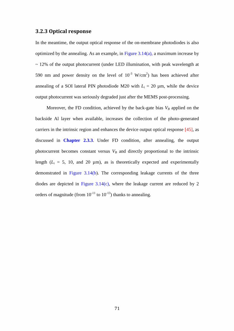
71
3.2.3 Optical response
In the meantime, the output optical response of the on-membrane photodiodes is also
optimized by the annealing. As an example, in Figure 3.14(a), a maximum increase by
~ 12% of the output photocurrent (under LED illumination, with peak wavelength at
590 nm and power density on the level of 10-3
W/cm2) has been achieved after
annealing of a SOI lateral PIN photodiode M20 with Li = 20 µm, while the device
output photocurrent was seriously degraded just after the MEMS post-processing.
Moreover, the FD condition, achieved by the back-gate bias VB applied on the
backside Al layer when available, increases the collection of the photo-generated
carriers in the intrinsic region and enhances the device output optical response [45], as
discussed in Chapter 2.3.3. Under FD condition, after annealing, the output
photocurrent becomes constant versus VB and directly proportional to the intrinsic
length (Li = 5, 10, and 20 µm), as is theoretically expected and experimentally
demonstrated in Figure 3.14(b). The corresponding leakage currents of the three
diodes are depicted in Figure 3.14(c), where the leakage current are reduced by 2
orders of magnitude (from 10-11
to 10-13
) thanks to annealing.

72
Figure 3.14 Output photocurrent of the on-membrane diode under LED illumination (~ 590
nm, ~ 10-3
W/cm2), with varied back gate voltage and reverse bias 2.0 V: the diode with Li =
20 µm before and after annealing (a), the diodes with Li = 5/10/20 µm after annealing (b);
leakage current in the on-membrane diodes (Li = 5/10/20 µm), as a function of back gate
voltage, before and after annealing (c).
A further improvement of optical dynamic (OD) is also achieved in the SOI
lateral PIN diode after annealing. As OD defined in equation (1.25), based on the
leakage current level in Figure 3.14(c), the OD increases from 102 to 10
4 under LED
illumination (with power density ~ 10-3
W/cm2), and from 10
1 to 10
3 under
monochromatic illumination (with power density ~ 10-5
-10-4
W/cm2).

73
3.2.4 Carriers’ lifetime and surface recombination velocity
A quantitative difference of dark currents between the on-substrate and on-membrane
diodes before and after annealing could be induced by the carriers’ effective lifetime
and surface generation-recombination (G-R) velocities.
Taking the device samples with aluminum deposited on the backside or with
metal back contact, we further apply the reverse- and forward-biased gated-diode
techniques described in [64] [34] (Annex 1), in order to estimate the effective carriers’
lifetime eff and back surface generation-recombination velocity s of the experimental
devices presented in Figure 3.13 and Figure 3.14. This yields values of eff and s in the
ranges of 0.02-0.2 µs and 180-230 cm/s in the M10 devices before annealing, 1-3 µs
and 25-32 cm/s in the M10 after annealing, and 2-6 µs and 3-10 cm/s in the reference
S10 devices in Figure 3.13. Improved eff and s values in M10 devices after annealing
qualitatively correlate with leakage current comparisons and validate the device
improvement by the low-temperature annealing [60].
For devices with three different Li = 5, 10 and 20 µm in Figure 3.14(c), carriers’
lifetime and surface generation-recombination velocity have also been extracted:
before annealing, carriers’ effective lifetime eff of the on-membrane diodes is 0.05-
0.5 µs, the surface generation-recombination velocity s is 90-180 cm/s; after annealing,
the values yield 2-10 µs for eff and 4-12 cm/s for s. These show an improvement by a
factor of about 2 orders of magnitude when compared to the values before annealing
(which can be correlated with the leakage current measurements) and hence become
close to the values measured for the on-substrate diodes without DRIE and aluminum
backside deposition [65].
For the on-membrane diodes M10 after annealing and the on-substrate diodes
S10, there is almost one order of magnitude difference shown in the diode leakage

74
current values in Figure 3.13 and Figure 3.14(c), whereas the extracted eff and s
values are quite close or at the same level. Hence, besides the carriers’ effective
lifetime and surface generation-recombination velocity, there could be other factors
which affect the diode leakage current characteristics.
3.2.5 Low-frequency noise characterization
To obtain further insights on the device performance, low-frequency noise (LFN)
characterization has been performed at RT under forward bias condition in frequency
f range 100-10
6 Hz using Keysight A-LFNA noise system. The normalized noise
spectral densities are presented in Figure 3.15(a) [60], for the on-substrate (S10,
dashed curves) and on-membrane (M10, solid curves) diodes, both with and without
Al deposition. The inset to Figure 3.15(a) depicts the forward current-voltage (I-V)
characteristics of the corresponding devices. Normalization of the low-frequency
noise spectra is done to the square of the forward current IF2 at a specific forward
voltage of 0.65 V or 0.75 V where IF is ~ 10-5
A. In the considered bias range, the
diode ideality factor ƞ [7] is ~ 1 for the reference device S10, indicating dominance of
diffusion current, while factor η is ~ 2 for M10 indicating dominance of generation-
recombination mechanisms. In correlation, typical 1/f flicker noise [66] [67] is
observed in the S10 reference device in all cases, while generation-recombination (G-
R) noise SI is observed in the M10 devices with and without Al deposition before any
annealing. The spectral density of the G-R noise is represented by the Lorentzian
function SI (f) = S0 / [1+(2πfτ)2] [68], i.e. corresponding to the low-frequency plateau
and 1/f2 trend indicated in Figure 3.15(a), where S0 is the frequency independent part
of SI (f) observed at f < (2πτ)-1
and τ is the time constant associated with a specific
trapping state [68]. As G-R noise in semiconductors originates from one or several
discrete traps that randomly capture and emit carriers [69], it can be concluded that

75
devices M10 are degraded with respect to device S10 and discrete traps have been
introduced by the MEMS post-processing DRIE. It is also worth noting that
backside
Al deposition results in a significant increase of noise both in the case of S10 and
M10 devices (Figure 3.15(a)), indicating further process-induced degradation [67]
[68].
The normalized LFN spectral densities of devices after annealing are presented
in Figure 3.15(b), at anode voltage of 0.75 V where device forward current IF is ~10-5
A. Typical 1/f noise is now measured in the M10 devices, instead of the observed G-R
noise before annealing (Figure 3.15(a)). This suggests a trap neutralization achieved
by the low-temperature local annealing performed on the M10 devices. Worth to
mention is that the corresponding forward I-V characteristics of M10 device become
close to those of the S10 devices with ƞ ~ 1, as well as the level of noise. Furthermore,
the 1/f noise in the S10 device with Al after annealing is also back to the level of the
noise in the reference S10 without Al, implying an improvement of device with Al
deposition by annealing.

76
Figure 3.15- Measured low-frequency noise spectral density, normalized to square of forward
current, SI/IF2, at an anode bias of 0.65 V or 0.75 V with IF ~ 10
-5 A, for the SOI lateral PIN
diodes M10 and S10 respectively, with and without Al deposition, before annealing (a) and
after annealing (b). The insets depict the device forward current-voltage (IF-V) characteristics
under the noise measurements, with corresponding curve styles.

77
3.3 Simulation and analysis of diode reverse
leakage current
Based on the experimental observation of the post-processing and local annealing
impact on the diode forward and reverse performance and considering interface traps
and the extracted carriers’ lifetime and surface recombination velocity, two-
dimensional (2-D) device simulations of the reverse leakage current will be deeply
investigated in this part, to understand the origin of the degradation induced by the
MEMS post processing and identify the mechanisms in device leakage behavior, to
propose solutions to optimize device performance.
3.3.1 A suspended SOI PIN diode without gate
A 2-D physical model (i.e. a single SOI lateral P+/P
-/N
+(PIN) diode) is primarily
defined in Atlas/SILVACO [40], as presented in Figure 3.16. Based on typical SOI
technology, fixed oxide charge Qoxf in the front oxide is 1×10¹¹
cm-2
, Qoxb in the back
buried oxide is 6×10¹⁰
cm-2
. In this case, back gate is out of consideration, i.e. gate
bias is 0 V.
Figure 3.16- Schematic view (not to scale) of a single SOI lateral PIN diode (Li = 10 µm) in
Atlas/SILVACO. Symbols ‘+’ represent fixed oxide charges.
Using the extracted parameters (the effective carriers’ lifetime eff and back

78
surface generation-recombination velocity s) in the on-membrane and on-substrate
diodes into the Atlas/SILVACO device model (i.e. the diodes with Li = 10 µm),
Figure 3.17 presents the simulated dark current versus temperature, under reverse bias
of 2.0 V. One best-case dark currents for the on-membrane and on-substrate diodes
are simulated with parameters (i.e. simulation 1 in Figure 3.17): 0.5 µs and 90 cm/s, 9
µs and 1 cm/s respectively; one worst-case dark currents simulated with parameters
(i.e. simulation 2 in Figure 3.17): 0.05 µs and 180 cm/s for the on-membrane diode, 6
µs and 3 cm/s for the on-substrate. Good qualitative agreement of dark currents can be
primarily appreciated between the experimental data in Figure 3.12 and the simulation
results in Figure 3.17. We therefore confirm that the MEMS post-processing DRIE
used to fabricate the circular membrane degraded the device carriers’ lifetime and
surface generation-recombination velocities, leading to more than ten times higher
dark currents for the diodes on the suspended platform.
To get more insight into the physics, as presented in Figure 3.17, under reverse
bias of 2.0 V, the dark currents increase following the silicon intrinsic carriers
concentration ni dependence on temperature T, confirming that the dark current is
dominated by thermal volume (Shockley-Read-Hall) generation current Irg in the
intrinsic region as given in equation (3.7) [8]. The current is hence proportional to the
length of depletion region Lzd, where the diode is without back gate. Carriers’
effective lifetime τeff for the on-membrane and on-substrate diodes is also introduced
below.
(3.7)
(3.8)
where m is the number of the parallel diode fingers, W is the device width, dSi is the
79
thickness of active silicon film, Ut is the thermal voltage, τ is the carriers’ lifetime in
volume, and s0 and st are the carrier surface generation-recombination velocities at the
front and back oxide interfaces, respectively. The simulated dark currents of Figure
3.17 in the on-membrane and on-substrate diodes with Li = 10 µm, are very similar
and with good both qualitative and quantitative agreement to the experiment data
presented in the on-substrate diodes and the diodes M10 before Al deposition in
Figure 3.12.
Figure 3.17- Dark current versus temperature simulated in Atlas/SILVACO with varied τ (in
µs) and SRV (in cm/s), in single diodes (Li = 10 µm) on membrane (simulation1: 0.5 µs, 90
cm/s; simulation2: 0.05 µs, 180 cm/s) and on substrate (simulation1: 9 µs, 1 cm/s;
simulation2: 6 µs, 3 cm/s), without gate biasing and at reverse bias 2.0 V.
3.3.2 A suspended SOI PIN diode with traps and gate bias
In relation with experimental characterizations and extraction, we further conduct
device simulation in the suspended SOI lateral PIN diode with a back gate control,
specifically implementing interface traps, carriers’ lifetime and fixed oxide charges, to
qualitatively analyze the leakage current, get a physical insight on the generation

80
mechanisms in the diode leakage behavior and identify the dominant mechanism in
different operation regimes and conditions.
3.3.2.1 Two-dimensional device model in Atlas/SILVACO
Figure 3.18 schematically presents the simulated two-dimensional (2-D) device cross-
section in Atlas/SILVACO [40], which corresponds to the experimental diode with Al
back gate shown in Figure 3.2(a). Similarly to experimental devices M10, the width of
the simulated diode is 60 m, the length of the P- region (i.e. intrinsic length Li) is 10
m, the length of the P+ and N
+ regions is 2.5 m, the active Si film thickness is 250
nm, the buried oxide thickness is 1.0 m. The multilayer stack and its corresponding
material thickness are fixed according to Table I. The doping levels of the P+, P
- and
N+ region are respectively 1×10
20, 5×10
15 and 1×10
20 cm
-3. The backside 1 m-thick
Al layer is used as back gate electrode. Contacts of the anode and cathode electrodes
are Ohmic.
Figure 3.18- Schematic view (not to the scale) of the single SOI lateral PIN diode M10 with
Al back gate, in Atlas. Symbols ‘+’ represent fixed oxide charges, symbols ‘×’ represent
interface traps.
As the G-R noise observed at low frequency in the M10 devices indicates

81
discrete traps existence, interface traps Dit (both acceptor- and donor-like types) are
introduced at both front and back SiO2/Si interfaces of the I-region. The interface trap
setting based on Figure 10.10 of [48] (Annex 2). The acceptor- and donor-like traps
are symmetrically distributed in the upper and lower parts of Si band gap with two
density peaks (~ 1×10¹²
cm-2
eV-1
) at 0.12 eV of Ec − Et (for the acceptor-like traps
DitA) and Et − Ev (for the donor-like traps DitD), where Et is the trap energy position in
the band gap, Ec is the conduction band energy of Si, and Ev is the valence band
energy of Si. Depending upon the Fermi level position, the interface traps can be
charged or discharged. An acceptor-like trap is negatively charged (i.e. ionized and
filled with an electron) when the Fermi level is above the trap energy level, and kept
neutral when the Fermi level is below the state (i.e. empty) [2]. A donor state is
neutral if the Fermi level is above it (i.e. the state is occupied) and positively charged
when it is empty [2]. In this study, when the position of the Fermi level in the front
and especially back surfaces is altered by the back gate bias VB, these interface traps
give rise to surface charges, negative for the acceptors and positive for the donors.
Next to that, fixed oxide charge densities Qox in the front gate oxide and in the BOX
are implemented into the simulations. Volume carriers’ lifetime is also specified
according to the experimental values.
3.3.2.2 On-membrane suspended device M10 without annealing
To get close to the practical conditions in the suspended M10 diode, several issues
need to be taken into account in the simulation: 1) as in [70] the acceptor-like traps
dominate in the P-type doped silicon film; 2) the M10 device was released by the
post-CMOS DRIE where the 1.0 m-thick buried oxide acts as the effective etch stop
layer [71] and thus the quality of the back interface can be assumed to be worsened
compared to the front SiO2/Si interface; 3) carriers’ lifetime is degraded by the

82
MEMS post processing, according to the experimental extraction.
Figure 3.19- Simulated leakage current and the corresponding surfaces potentials (a), and the
total, ITA, SRH G-R rates (b), in a single SOI lateral PIN diode M10, under a reverse bias 2.0
V, as a function of the back gate bias. Device parameters are set as: volume carriers’ lifetime
= 0.02 µs; interface traps DitA(f) = DitD(f) = 1×10¹²
cm-2
eV-1
at the front interface; DitA(b) =
1×10¹³
cm-2
eV-1
and DitD(b) = 1×10¹²
cm-2
eV-1
at the back interface; fixed oxide charges Qox(f)

83
= 1×10¹¹
cm-2
and Qox(b) = 2×10¹¹
cm-2
in the front oxide and BOX. The inset to Figure 3.19(b)
presents the detailed ITA G-R rates at the front and back interfaces.
The respective device parameters are therefore implemented as follows. At the
front interface, the maximum interface traps densities are DitA(f) = DitD(f) = 1×10¹²
cm-
2eV
-1. However, at the back interface, one order of magnitude higher value of the
acceptor-like traps density is implemented, i.e. DitA(b) = 1×10¹³
cm-2
eV-1
, while DitD(b)
is kept at the level of 1×10¹²
cm-2
eV-1
. Furthermore, volume carriers’ lifetime is set
to 0.02 µs, based on the experimentally extracted value before annealing. Fixed oxide
charges are Qox(f) = 1×10¹¹
cm-2
in the gate oxide and Qox(b) = 2×10¹¹
cm-2
in the BOX.
Simulation results of the PIN diode under a reverse bias of 2.0 V are presented
in Figure 3.19. In Figure 3.19(a), the back surface potential is changed from -0.5 to
2.5 V and the front surface potential from -0.2 to 0.5 V as back gate voltage VB
increases from -40 to 80 V. Back gate bias sweep in fact results in the space-charge
(SC) condition of the I-region at Si/BOX interface to be changed from accumulation,
to non-fully-depleted (NFD) condition, then to fully-depleted (FD) condition (above 0
V here), finally to strong inversion. Under FD conditions, VB sweep also induces
variation of the surface potential at the front interface. The simulated leakage current
amplitude and its variation with VB qualitatively correspond to the experimental
leakage current of the M10 device before annealing (Figure 3.13). Under
accumulation, the diode leakage current is ~ 10-12
A; under FD condition, the leakage
current increases to a plateau of 10-11
A. To detail the leakage behavior in the PIN
diode, we probe the generation-recombination (G-R) rates in the whole I-region. They
are presented as total G-R rates and separate interfaces trap-assisted (ITA) and
“volume” SRH rates in the I-region in Figure 3.19(b). Under the FD conditions,
before the Si/BOX interface of the I-region goes into the strong inversion (i.e. VB < 36

84
V), the ITA process dominates in the diode leakage behavior. As detailed in the
corresponding inset, the total ITA G-R rate is mainly contributed by the back interface,
due to higher density of DitA(b) and also larger variation of the back surface potential
(altered from -0.5 to 2.5 V). When the I-Si/BOX interface is under the strong
inversion condition, i.e. VB > 36 V, the “volume” SRH (with = 0.02 µs) mainly
contributes to the diode leakage current. The total SRH rate in the whole I-region is
typically dominated by the volume SRH and dependent on the volume carriers’
lifetime τ [43].
Figure 3.20- Simulated leakage current and the corresponding SRH G-R rates in a single SOI
lateral PIN diode M10, with variation of carriers’ lifetime = 0.02, 0.05, 0.1, 0.5 µs, based on
the interfaces traps DitA(f) = 1×10¹²
, DitD(f) = 1×10¹²
cm-2
eV-1
, and DitA(b) = 1×10¹³
, DitD(b) =
1×10¹²
cm-2
eV-1
and the fixed oxide charges Qox(f) = 1×10¹¹
, Qox(b) = 2×10¹¹
cm-2
.
Effect of the volume carriers’ lifetime variation on the simulated leakage

85
current and the corresponding SRH G-R rates is presented in Figure 3.20. One can see
that the SRH rate decreases with the increase from 0.02 to 0.5 µs and reaches its
maximum when the I-region enters in a full depletion (VB > ~ 6 V). Moreover, the
“volume” SRH process starts to play a dominant role in the diode leakage after the I-
Si/BOX interface goes into strong inversion (VB > 36 V). As a result, the leakage
current in this region is sensitive to the value of (notably, it increases with
reduction).
Figure 3.21- Simulated leakage current and the corresponding ITA and SRH G-R rates, with
three different settings of the fixed oxide charges: Qox(f) = 2×10¹¹
and Qox(b) = 4×10¹¹
cm-2
,
Qox(f) = 1×10¹¹
and Qox(b) = 2×10¹¹
cm-2
, Qox(f) = 5×10¹⁰
and Qox(b) = 1×10¹¹
cm-2
; interfaces
traps densities are DitA(f) = DitD(f) = 1×10¹²
cm-2
eV-1
, DitA(b) = 1×10¹³
, DitD(b) = 1×10¹²
cm-2
eV-1
;
volume carriers’ lifetime = 0.02 µs.
Effect of the fixed oxide charge is presented in Figure 3.21. The diode leakage
current characteristics are positively shifted (by ~ 10 V) with the positive fixed oxide

86
charges reduction from Qox(f) = 1×10¹¹
cm-2
, Qox(b) = 2×10¹¹
cm-2
(the dashed line) to
Qox(f) = 5×10¹⁰
cm-2
, Qox(b) = 1×10¹¹
cm-2
; while negatively shifted with the oxide
charges increased to Qox(f) = 2×10¹¹
cm-2
, Qox(b) = 4×10¹¹
cm-2
. Observed leakage
current behavior correlates with the trends in the detailed ITA and SRH G-R rates
obtained with the Qox variation (Figure 3.21).
Thus, deviation observed in the leakage current characteristics (e.g. current
variation and shift) for the same kind of the practical devices, i.e. device-to-device
variation (Figure 3.13), can be qualitatively explained by the varied and Qox for the
specific interfaces traps condition.
3.3.2.3 On-membrane suspended device M10 after annealing
Considering the trap neutralization observed in the LFN characteristics of the M10
after annealing (Figure 3.15), the acceptor-like traps density at the back interface are
set to 1×10¹²
cm-2
eV-1
, i.e. one order of magnitude lower with respect to the case
“M10 before annealing”. Therefore, the front and back interfaces trap densities are as
follows: DitA(f) = DitD(f) = DitA(b) = DitD(b) = 1×10¹²
cm-2
eV-1
. Fixed oxide charges are
reduced to Qox(f) = 5×10¹⁰
cm-2
, Qox(b) = 1×10¹¹
cm-2
. The simulations are performed
for the two cases of the volume carriers’ lifetime = 0.1 and 1.0 µs, i.e. close to the
experimentally extracted values.
As shown in Figure 3.22(a), the simulated diode leakage currents are on the
level of 10-13
A under the accumulation of I-Si/BOX interface and increase to over 10-
12 A when the I-region goes into FD condition. The detailed G-R rates for this case are
presented in the corresponding inset. One can see that the ITA plays a dominant role
in the diode leakage with the interface trap density of 1012
cm-2
eV-1
and of 0.1 µs.
With the volume lifetime increase from 0.1 to 1.0 µs, a slight decrease of the leakage
current is observed due to the decreased SRH rates, but still on the level of 10-12
A

87
under FD condition.
Figure 3.22- Simulated leakage current as a function of back gate bias, under a reverse bias of
2.0 V; volume carriers’ lifetime = 0.1 and 1.0 µs: DitA(f) = DitD(f) = DitA(b) = DitD(b) = 1×10¹²
cm-2
eV-1
, Qox(f) = 5×10¹⁰
, Qox(b) = 1×10¹¹
cm-2
(a); no interfaces traps and no fixed oxide
charges (b). The inset to Figure 3.22(a) presents the ITA and SRH G-R rates for = 0.1 µs
with interfaces traps and oxide charges.
A presumably ideal condition is presented in Figure 3.22(b), when only volume
carriers’ lifetime (i.e. only “volume” SRH) is considered. Positive shift of the leakage
curves is observed due to the absence of fixed oxide charges. Under FD condition (i.e.
at a “maximum plateau” level), the leakage current is reduced due to the absence of
interfaces traps. The leakage current gets optimized on the level of 10-13
A in the case
of = 1.0 µs without traps. This “case” can serve as a very rough (first order)

88
representation of reference S10 device on the substrate. Indeed, experimentally
extracted surface recombination velocity (related to Dit) is much lower in the
reference S10 device than even in M10 device after annealing. Furthermore, leakage
current reduction and its shift to positive VB experimentally observed in S10 reference
device with respect to M10 device after annealing (Figure 3.13) correlate well with
fixed oxide charge reduction used in the above simulations of “ideal” device.
3.4 Summary
In this chapter, device degradation (e.g. trap introduction concluded from the low-
frequency noise characterization), which was induced by the MEMS post-processing
(DRIE and Al deposition), with regards to the diode forward and reverse
characteristics, is presented in details. A low-temperature annealing can be carried out
in situ (thanks to the embedded micro-heater for local heating and the PIN diode itself
for temperature sensing) to achieve trap neutralization and optimize the device dark
current characteristics in forward and reverse conditions, optical response and carriers’
lifetime and surface recombination velocity. And device stability (i.e. diode forward
characteristics) is recovered into the suspended diode after annealing and with back
gate bias to achieve FD condition of the I-region.
After annealing, there is one order of magnitude increase in both the diode dark
current and the corresponding output photocurrent under illumination, as the I-region
goes from the accumulation to the full depletion by the back gate biasing. The device
responsivity and QI are also optimized under the full depletion. However, device
optical dynamic is kept constant in the case where back gate biasing alters the
depletion condition in the I-region.

89
Numerical simulations have been performed in Atlas/SILVACO for deeper
analysis of the leakage current behavior in the lateral PIN diode before and after
annealing, and for identification of the generation mechanism dominating the diode
leakage behavior. The experimental and simulated behaviors of “as processed” and
annealed diode leakage current are shown to be in good qualitative agreement.
The study supports the full understanding of the behavior, modeling and
parameter extraction of the SOI lateral PIN diode for its use and optimization in
thermal and optical sensing applications.
90
CHAPTER 4
Optical optimization in a SOI
lateral PIN diode
In our SOI case, the optoelectronic device includes multilayer films. As depicted in
Figure 3.1 (in Chapter 3.1), besides the active silicon film lying on the silicon
substrate with a buried oxide layer, there is an oxidation layer beyond the active
silicon, a polysilicon layer for implantation protection and also a Si3N4 passivation
layer on the top for device reliability. When light is shined onto the device surface and
starts penetrating into the device, mutual interference of light among each single-layer
dielectric film needs to be taken into account.
In this chapter, we will discuss and analyze the light propagation in the
multilayer stack of the optical sensor (i.e. a SOI lateral PIN diode). Transfer matrix
method will be implemented to characterize and simulate the optical absorption in the
active silicon film. By using different backside reflectors (i.e. a gold bottom layer, an
aluminum backside layer, a black silicon wafer and a silicon substrate) placed below
the SOI lateral PIN diode, active light absorption in the I-region of the PIN diode can
be modulated. Correlating the specific optical response of the photodiodes with the
four backside reflectors, experimental characterization will be done to advance the
optical sensing capability and achieve the multi-wavelength detection within the
visible wavelength range.

91
4.1 Light propagation in multilayer stack films
4.1.1 Transfer matrix method
Based on the electromagnetic theory and combining with the boundary conditions for
the electric (E) and magnetic (B) fields of incident plane wave, a transfer matrix
method has been developed to represent the multilayer film of one device and
characterize optical performance, i.e. the reflectance, transmittance and absorption,
while light propagating through the device multilayer stack.
Figure 4.1 describes the interference diagram as light penetrates and propagates
through a single dielectric film [72]:
Figure 4.1- Light interference diagram as light penerating through a single dielectric film. (or
named as: reflection of a beam from a single layer. Note that a bold dot is used to denote
directions perpendicular to the plane of incidence)

92
The fields Ein and Bin at the incident (a) interfaces are related to the fields Eout and Bout
respectively at the output (b) interface, based on equation (4.1) [72]:
(4.1)
with
(4.2)
(4.3)
(4.4)
(4.5)
and the relevant parameters are defined as:
(4.6)
(4.7)
(4.8)
(4.9)
(4.10)
(4.11)
where the 2×2 matrix M is called the transfer matrix of single film l in Figure 4.1. θ0,
θt1 and θt2 are respectively the light incident angle, the refraction angle in the film l
and the refraction angle in the substrate. t is the thickness of the film l, δ is the phase
difference due to the traversal of the film l, c is the light speed in vacuum, and λ is the

93
incident light wavelength. no, n1 and ns are respectively the optical indices ( )
of the film materials, including the real (n) and imaginary (k) parts.
Generalizing, the light propagation through a multilayer-film stack, with S
layers, the overall transfer matrix M is represented as equation (4.12) [72]:
(4.12)
4.1.2 Reflectance, transmittance and absorption
Based on the transfer matrix equations (4.1) to (4.12), the reflectance R and
transmittance T can is defined by:
(4.13)
(4.14)
where r, t are respectively the reflection and transmission coefficients, defined as
(4.15)
(4.16)
For one light incidence, there is a simple relation among reflectance R,
transmittance T and absorption A [73]:
(4.17)
Applying the theory for the case of normally incident light (the most commonly found
in practice), where θ0 = … θts = 0, cosθ0 = …= cosθts = 1, the absorption A in the
multilayer-stack film can be calculated by combining with equations (4.1) to (4.17).
Implementing the transfer matrix method into Atlas/SILVACO [40] within a
device model (i.e. the SOI lateral PIN diode), the effective absorption in the active

94
silicon film and thereafter device responsivity can be simulated.
4.2 Device optical simulations with transfer
matrix method
4.2.1 With gold bottom reflector
Figure 4.2- Cross-section view of the SOI lateral PIN diodes with different backside
reflectors placed below: a gold finish layer (a), a black silicon wafer (b) and a silicon
substrate (c).
In the on-membrane structure, depicted in Figure 3.1, the ~ 5 µm-thick membrane is
transparent to visible light. As the device chips are mounted in a dual-in-line (DIL) 16
ceramic package over a gold finish bottom layer, the gold finish layer acts as a metal
back mirror to the on-membrane device. The cross-section view is shown in Figure
4.2(a). Light reflection from the bottom gold layer needs to be taken into account, as
gold material acting high reflectivity for wavelength > 450 nm [74]. In this case, the
multilayer stack of the SOI lateral PIN diode with gold bottom reflector is
Air/Si3N4/SiO2/Polysilicon/SiO2/Silicon/BOX/Air cavity/Gold bottom. To further
consider the intrinsic absorption in the on-membrane diode without light reflected
back into the active silicon film, a black silicon wafer is placed below the on-
membrane structure (in Figure 4.2 (b)) as an ideal absorber, with less than 1%
reflectivity to absorb all the light transmitted through the membrane. The multilayer
95
stack is therefore considered to be Air/Si3N4/SiO2/Polysilicon/SiO2/Silicon/BOX/Air.
While for the diode lying on silicon substrate (i.e. using silicon substrate as a backside
reflector, in Figure 4.2(c)), the multilayer stack is
Air/Si3N4/SiO2/Polysilicon/SiO2/Silicon/BOX/Silicon substrate.
Based on the description of the transfer matrix method, we know that besides
incident light wavelength λ, refractive index (n,k) of each film material, film thickness
t and light incident angle θ affect the multilayer film performance (i.e. transmittance,
reflectance, and absorption).
However, within the visible and near infrared (IR) wavelength range, light
absorption (i.e. imaginary part k of refractive index) exists in the polysilicon gate
layer, which was deposited by low-pressure chemical vapor deposition (LPCVD)
technology and implanted with boron ions [16]. For λ below 600 nm, optical
absorption of silicon nitride deposited by plasma-enhanced chemical vapor deposition
(PECVD) technology also needs to be considered, affected by the gas mixtures of
SiH4/NH3/N2 and the plasma excitation frequency [17].
According to the specific multilayer stacks of the SOI lateral PIN diodes with
gold, black silicon and substrate reflectors, we take the materials thickness in Table I
(in Chapter 3.1) as a reference and specifically set the optical indices of each material
film. Two-dimensional (2-D) device numerical simulations are performed in
Atlas/SILVACO [40], to analyze and investigate the optical performance of the SOI
lateral PIN diodes (Li = 10 µm) with the three different backside reflectors placed
below.
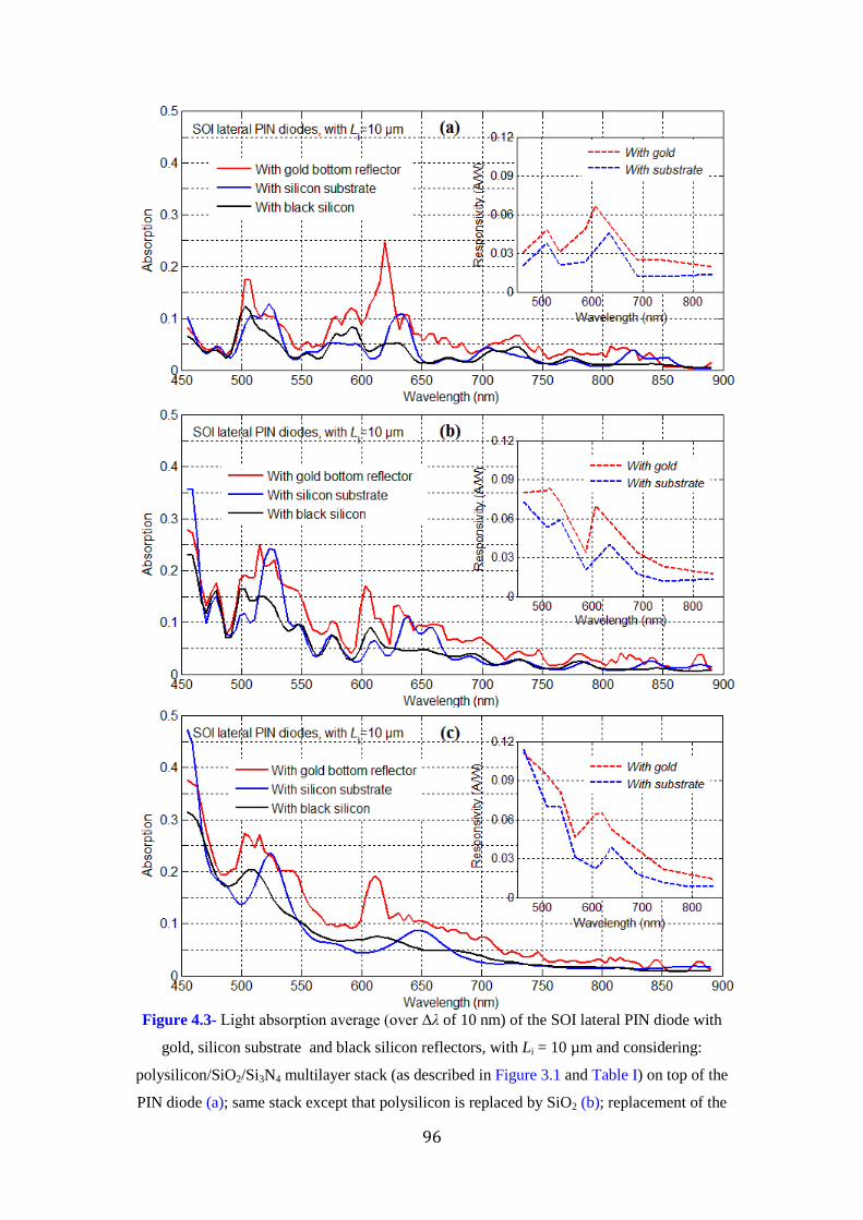
96
Figure 4.3- Light absorption average (over Δλ of 10 nm) of the SOI lateral PIN diode with
gold, silicon substrate and black silicon reflectors, with Li = 10 µm and considering:
polysilicon/SiO2/Si3N4 multilayer stack (as described in Figure 3.1 and Table I) on top of the
PIN diode (a); same stack except that polysilicon is replaced by SiO2 (b); replacement of the
97
previous stack by a single ARC layer of 85 nm-thick SiO2 directly on top of the PIN diode (c).
The corresponding insets represent the responsivities of the SOI PIN diodes with gold and
substrate reflectors simulated for the specific spectra taken from monochromator.
Under perpendicular light incidence, effective light absorption (i.e. available
photocurrent / source photocurrent) is extracted for single wavelength within 450-900
nm. Detailed results of absorption averaged (with bandwidth Δλ = 10 nm) for each 4
nm wavelength increment are presented in Figure 4.3(a). The solid red curve
represents the light absorption of the SOI lateral PIN diode considering the gold
bottom reflection (i.e. with gold bottom reflector), the blue curve is the optical
absorption of the on-substrate diode (i.e. with silicon substrate), and the black one is
the light absorption of the on-membrane diode, i.e. with black silicon wafer.
Thanks to the gold bottom reflection, for specific wavelength range (around 500,
600, 750 nm), light absorption in the on-membrane PIN photodiode can be improved
significantly, comparing to the diodes lying on the silicon substrate and with black
silicon placed below. The inset to Figure 4.3(a) presents the device responsivity,
simulated with the specific spectra that are taken from the monochromator in the
optical measurements. The dashed red curve is the simulated responsivity of the on-
membrane photodiode M10 with gold reflector, with peak responsivity of over 0.06
A/W at ~ 590 nm wavelength, the blue is for the on-substrate diode S10. Generally, a
global improvement of responsivity within 450-900 nm is achieved in the SOI diode
with gold bottom reflector, compared to the diode with silicon substrate. Furthermore,
light absorption in the diode with black silicon wafer is mostly close to and even
below the absorption in the diode with silicon substrate within 450-900 nm, while
higher merely in a few narrow ranges, e.g. around 590 nm and 740 nm wavelength,
which is due to light interferences in the device multilayer films and worth to be
investigated and validated in next measurements.

98
Polysilicon deposited in the 1.0 µm SOI CMOS technology for implantation
protection of the intrinsic region in SOI PIN photodiode, leads to unnecessary high
absorption especially for λ below 600 nm and reduces the diodes optical response in
Figure 4.3(a). Replacing the 300 nm-thick polysilicon with SiO2 as implantation
protection layer, optical simulated results for the diodes with the updated layer stack
and identical geometries are presented in Figure 4.3(b). Compared to the light
absorption in Figure 4.3(a), large improvement within 450-550 nm has been achieved,
thanks to the replacement of polysilicon with SiO2. Considering the gold bottom
reflection, the on-membrane diode (red curve) still achieves optical absorption
improvement and the simulated responsivity in the inset to Figure 4.3(b) yields over
0.08 A/W with λ below 520 nm.
Moreover, in a post-CMOS process, all the layers above the active silicon film
could be etched and replaced with a single thin ARC layer, i.e. 85 nm-thick SiO2.
Simulation results in Figure 4.3(c) show the boost of light absorption in the short
wavelength range (450-500 nm) and the responsivity of on-membrane diode (Li = 10
µm) with gold reflector, as shown in the corresponding inset, could be increased up to
0.09-0.11 A/W within 450-520 nm wavelength range.

99
4.2.2 With aluminum backside reflector
Figure 4.4- Cross-section view of a SOI lateral PIN diode with aluminum backside reflector.
Considering the MEMS post-process, instead of depositing gold as in [75] that is not
directly CMOS compatible, aluminum is implemented due to its feasibility. Moreover,
the aluminum material presents its stable and excellent reflectivity (i.e. over 90%)
within the whole wavelength range 200-1200 nm [74] while the gold material only
presents high reflectivity for wavelength > 450 nm. A second set of device optical
simulation has been performed in Atlas/SILVACO [40], mainly focusing on the on-
membrane device with aluminum (Al) backside layer as reflector. The cross-section
view of the SOI lateral PIN diode with aluminum backside reflector is depicted in
Figure 4.4, where the device multilayer stack is
Air/Si3N4/SiO2/Polysilicon/SiO2/Silicon/BOX/Aluminum. Another series of material
thicknesses have been implemented into the diode model, as a thickness variation of
each film (within ± 8-15%) could occur in practice during the device fabrication.
Light absorption in the active silicon film of the lateral SOI PIN photodiodes is
simulated within the 450-900 nm range. Figure 4.5 shows the detailed results of
absorption averaged over a bandwidth of 10 nm, including the SOI lateral PIN diode
with 1 µm-thick backside Al layer (green curve), the diode lying on substrate (blue

100
curve) and for the suspended photodiode without reflector, i.e. black silicon (black
curve). Again the light absorption below 480 nm is impaired due to high absorption in
the 300 nm-thick polysilicon layer that is used here to protect the I-region of the PIN
photodiode from implantation in SOI CMOS technology. In comparison with the two
other diodes (i.e. with silicon substrate and black silicon placed below), light
absorption in the suspended diode with Al appears obviously boosted at specific
wavelength ranges, e.g. around 500, 600 and 770 nm, due to the excellent reflectance
from the back Al reflector.
Quantitative deviations between the numerical simulations in Figure 4.3(a) and
Figure 4.5, including slight shifts in peaks and valleys of optical absorption, mainly
results from the process tolerance and hence the specific series of slightly different
materials thicknesses used into the two simulation set-up.
Figure 4.5- Light absorption averaged on a bandwidth of ~ 10 nm for the SOI lateral PIN
diodes with aluminum (green curve), silicon substrate (blue curve) and black silicon (black
curve) backside reflectors, with Li = 10 µm.
In this work, we extend the optical simulation of the SOI lateral PIN diode with
four backside reflectors to full experimental characterizations, in order to advance the

101
optical sensing capability of the SOI lateral PIN diode and develop its potential
applications.
4.3 Experimental characterization of device
responsivity
4.3.1 Measurement set-up at room temperature
Experimental characterization of the SOI lateral PIN photodiodes with the 4 backside
reflectors has been extensively carried out at room temperature. The set-up for the
visible and near IR wavelength range (450-900 nm) measurement consists of four
main parts: light source, measurement circuit, semiconductor analyzer and electrical
power supply, as depicted in Figure 2.10. For the light supply, we use Muller LXH
100 light source and a monochromator to select single wavelength λ (within 450-900
nm) with bandwidth Δλ ~ 10 nm. The incident light power densities for the specific
wavelengths under test (i.e. 462, 486, 510, 536, 550, 566, 586, 602, 620, 638, 658,
690, 742, 794, 854 nm) are on the level of 10-5
-10-4
W/cm2, measured by power meter
Ophir Nova 1Z01500. The device chips are mounted in a dual-in-line (DIL) 16
ceramic package over a gold finish bottom layer (the layer is used for the case of the
diode with gold bottom reflector in Figure 4.2(a)) and embedded in a printed circuit
board (PCB) for the test.
Before extracting the device responsivity, linearity in the device optical
response is presented in Figure 4.6, representatively with light wavelength of 586 nm
selected from monochromator. Increasing the incident power density, net
photocurrents from the diodes M10 and S10 increase linearly with the power density.
Then the devices on one chip are all measured during the same illumination session.
Each measurement is conducted three times on different chips.

102
Figure 4.6- Net photocurrents in diodes M10 and S10 with increase incident power density, at
wavelength of 586 nm.
4.3.2 Responsivity versus intrinsic length
Responsivity R of the lateral PIN photodiode is defined as [65]:
(4.18)
where Jph is the total photocurrent density, A is the photocurrent flowing area, i.e. the
device photosensitive surface area, and Pin is the incident optical power to the device
total surface area, Φin is the incident optical power density, Atot is the device total
surface area.
In this thesis, R increases with the length (i.e. Li = 5, 10, and 20 µm) of the
intrinsic region where the photo-generated carriers drift and diffuse eventually leading
to the photocurrent flow, because of the percentage of device photosensitive area
A/Atot (respectively, 30/58, 40/60, and 40/52) increasing with Li, as illustrated in Table
II.
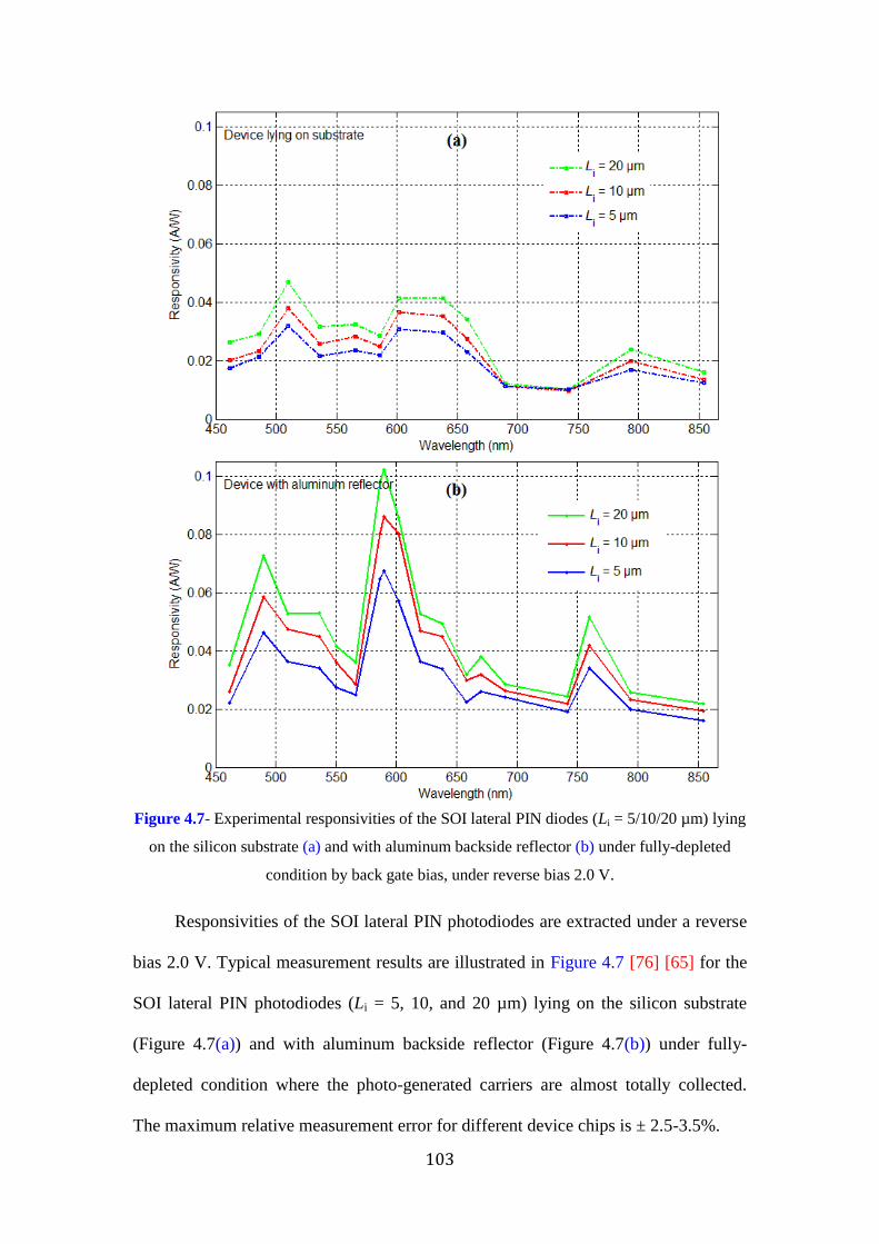
103
Figure 4.7- Experimental responsivities of the SOI lateral PIN diodes (Li = 5/10/20 µm) lying
on the silicon substrate (a) and with aluminum backside reflector (b) under fully-depleted
condition by back gate bias, under reverse bias 2.0 V.
Responsivities of the SOI lateral PIN photodiodes are extracted under a reverse
bias 2.0 V. Typical measurement results are illustrated in Figure 4.7 [76] [65] for the
SOI lateral PIN photodiodes (Li = 5, 10, and 20 µm) lying on the silicon substrate
(Figure 4.7(a)) and with aluminum backside reflector (Figure 4.7(b)) under fully-
depleted condition where the photo-generated carriers are almost totally collected.
The maximum relative measurement error for different device chips is ± 2.5-3.5%.

104
In experiments, we see that the responsivity indeed increases with the device
intrinsic length Li, as theoretically investigated. Responsivities obtained in the
experimental on-substrate diode with Li = 10 µm in Figure 4.7(a) has quantitatively
validated the absorption and responsivity simulated in Figure 4.3(a). For example,
there is peak responsivity (~ 0.03 A/W) at ~ 490 nm wavelength both in the
measurement and the simulation fitting.
In the SOI lateral PIN diode with aluminum (Al) backside reflector, responsivity
peaks are observed at ~ 490, ~ 590, and 760 nm, which firstly validate the device
optical simulation (i.e. the effective light absorption) in Figure 4.5 and further result
in high potential for blue, yellow and near IR light detection. Compared to the
responsivity of the on-substrate diode, a strong responsivity increase (over 2~3
improvement) in the diodes with Al reflector has been observed due to the excellent
reflectance from the backside Al layer. At reverse bias 2.0 V and under FD condition
(leading to the most efficient collection of photo-generated carriers), responsivity R in
the SOI photodiode with Li = 20 µm at RT for 3 different wavelengths (490, 590 and
760 nm) are 0.07, 0.1, 0.05 A/W respectively. Moreover, R increases with Li yielding
0.061, 0.079, 0.1 A/W at 590 nm for device M5, M10, M20 with Li = 5, 10, 20 µm,
respectively.
Compared to the photodiode of [24] with the same intrinsic length, the
maximum responsivity of 0.1 A/W at ~ 590 nm is improved by ~ 2 in our device
with the Al backside reflector and gate.
4.3.3 Responsivity versus backside reflectors
As varied light absorption in the active Si film results from the different backside
reflectors (i.e. gold bottom layer, silicon substrate, black silicon wafer and aluminum
backside reflector), 4 specific output photocurrents have been experimentally obtained
105
under same incident illumination. Typical responsivities of the lateral PIN
photodiodes (for Li = 10 µm) with the 4 backside reflectors are presented in Figure 4.8
[65], where the maximum relative measurement error for different device chips is ±
4.2-7.0%.
At RT, responsivities of the on-membrane photodiode with gold bottom
reflector yield 0.02-0.06 A/W within 450-900 nm wavelength range. While compared
to the PIN diode with black silicon wafer placed below (black curve in Figure 4.8),
higher responsivity in the on-membrane diode with gold reflector (red curve) has been
globally observed within 450-900 nm wavelength range. It is because the light
transmitted through the membrane can be reflected back into the active Si layer by the
gold bottom mirror, instead of being absorbed by the black silicon wafer, as depicted
in Figure 4.2(b). Furthermore, compared to the on-substrate photodiode, the on-
membrane diode with gold reflector globally achieves higher responsivities, shown
nearly 50% improvement in average. For some specific wavelengths (around 500, 600,
750 nm), the responsivities for the on-membrane diodes increase by 1.5-2.5. It
demonstrates that the reflection from gold bottom of the device package has
significantly improved the responsivity of photodiodes on the suspended micro-
hotplate platform, in the visible and near IR wavelength range.
Moreover, the responsivity of the photodiode with black-silicon reflector in
Figure 4.8 is mostly close to and even less than the responsivity of the on-substrate
diode (blue curve) within 450-900 nm, while higher only at ~ 590 and ~ 740 nm, as
firstly indicated in the simulations of Figure 4.3(a), due to light interferences in the
device multilayer films.
Generally, there is good agreement between the simulated effective optical
absorption and the experimental responsivity in the photodiodes with the 4 backside

106
reflectors. Qualitatively, the peaks observed in the simulation are validated in the
experimental responsivity. Quantitatively, the improvement of optical response
compared to the photodiodes with different backside reflectors is primarily simulated
with two series of thickness separately set into the multilayer stacks of Figure 4.3(a)
and Figure 4.5, then experimentally characterized in Figure 4.8.
Figure 4.8- Typical responsivities of the SOI lateral PIN diodes with 4 different backside
reflectors: aluminum backside reflector, gold reflector, black silicon wafer and silicon
substrate.
Good agreement is achieved between the device experimental characterization
and the device numerical simulations. A global improvement of optical response
within 450-900 nm has been simulated in Figure 4.3(a) and validated in measurements
(Figure 4.8) in the SOI diodes with gold bottom reflector, compared to the diode with
silicon substrate and with black silicon wafer. Similarly, the experimental drops
observed at wavelengths around 540 and 700 nm are also confirmed, qualitatively
supported and explained by the absorption simulations, as well as the ranges of

107
wavelengths around 510, 640 and 800-850 nm where the on-substrate photodiode
response is the closest to the on-membrane with gold reflector.
Remaining quantitative deviations between measurements and simulations,
including slight shifts in the peaks and valleys of optical responses, could result from:
a.) the exact thicknesses of films in the device multilayer stack, as a thickness
variation of each film (within ± 8-15%) could occur in practice during the device
fabrication; b.) the exact optical indices of all the materials, as their properties depend
on the technology and practical process conditions; c.) device electrical conditions,
e.g. carrier lifetime and surface recombination velocity.
4.4 Light discrimination and high-temperature
applications
4.4.1 Multiple-wavelength detection
Among the individual SOI lateral PIN diode with the gold, aluminum, substrate or
black-silicon backside reflector, the photodiode with the aluminum reflector directly
shows its remarkable potential in blue (~ 490 nm), yellow (~ 590 nm) and near IR (at
760 nm) lights detection. However, the 4 specific output signals (i.e. measured
photocurrents or extracted responsivities) have been uniquely obtained under same
incident illumination (with the same incident wavelength, and its corresponding
bandwidth and power density), from the photodiodes with the 4 backside reflectors.
To advance the optical sensing capability and target on the multiple-wavelength
detection within the visible and near IR light range (450-900 nm), wavelength sensing
is therefore proposed by correlating the responses of the diodes with the 4 backside
reflectors.

108
To compare the photocurrents obtained from the 4 photodiodes under same
illumination, mathematical ratios of the 4 measured photocurrents have been
computed to specifically detect the incident light wavelength. This technique could
have as advantages to be independent of incident light power and to enable the
resolution of ambiguities between peaks under unknown light power, since neither the
absolute photocurrent amplitude which depends on the incident optical power density
nor the absolute device responsivity need to be taken into account to discriminate the
light wavelength.
Figure 4.9 [65] shows the mathematic ratios between the measured optical
signals from the photodiodes with the 4 different backside reflectors under same
incident illumination: the ratios of aluminum/gold (X), black-silicon/substrate (Y) and
gold/black-silicon (Z, represented by the color bar). The rectangles filled with color
represent the minimum and maximum ratio values, considering the experimental
variations resulting from different device chips and intrinsic lengths Li = 5, 10, and 20
µm.
By calibrating the specific values of the set of ratios (X, Y, Z), as illustrated in
Figure 4.9, the light wavelength could be discriminated. For example, the 742 nm-
wavelength light detection shows a unique and non-ambiguous correspondence to the
(0.8, 1.5, 1.8) set. Other such correspondences could be specifically attributed to
multiple wavelengths (e.g. at 462, 486, 536, 550, 566, 586, 602, 620, 742, 760, and
794 nm in Figure 4.9).
On the basis of such multiple-wavelength detection, red-green-blue (RGB)
sensing application could be targeted based on a simple sensor design for the red (620
nm), green (566 nm) and blue (462 nm) lights discrimination. The application can be
explored for the design of a compact oxygen sensor without using any optical filters,

109
for luminescence emission at 620, 760 nm. Another potential application could
envisage compact in-situ plasma monitoring system setup with specific and
simultaneous detection of spectral lines at e.g. 486, 586, and 742nm.
Figure 4.9- Mathematic ratios among the measured optical signals from the photodiodes (Li =
5/10/20 µm) with the 4 different backside reflectors: the ratios of aluminum/gold (X), black-
silicon/substrate (Y) and gold/black-silicon (Z).
4.4.2 High-temperature application
Targeting high-temperature application of the SOI device, measurement with
increasing temperature is considered. Device samples are measured on the
temperature-regulated wafer chuck of a probe station (PM8PS), and semiconductor
device analyzer (Agilent, B1500A) is used to obtain the experimental curves. In this
set-up, high-power LEDs are used as stable light source: blue LED (peak at 480 nm)
and yellow LED (peak at 596 nm), due to the incompatibility between PM8PS and the
monochromator. Both light power densities are on the order of 10-3
W/cm2.

110
Dividing the currents of each device by the number of the in-parallel diodes, the
measured photo (= total current – dark current) and dark currents (under reverse bias
2.0 V) for single-finger diodes with Li = 5, 10, and 20 µm are plotted in Figure 4.10
(a), where blue LED (wavelength peak at 480 nm) is used as light source and
temperature varies from RT to 200 °C.
Up to about 200 °C, the photocurrents of the on-membrane photodiodes can be
discriminated from the increasing dark currents, where the dark current is dominated
by thermal volume (Shockley-Read-Hall) generation current Irg in the intrinsic region
as discussed in Chapter 3.3.1. Another validation is done with the yellow LED
(wavelength peak at 596 nm) as light source in Figure 4.10(b). The on-membrane
diodes with the metal bottom reflector continuously achieve an improved optical
response in comparison to the on-substrate photodiodes. At room temperature, the
extracted responsivities of devices M20 and S20 are, respectively, 0.0471 and 0.0318
A/W at wavelength 480 nm, and 0.0547 and 0.0359 A/W at wavelength 596 nm.
There is more than 50% improvement of responsivities in the on-membrane device
M20 with bottom mirror while in comparison with the on-substrate diode. And the
optical response (i.e. responsivities) in the yellow range is 12-16% higher than that in
the blue range. These are consistent with the respectively measured responsivities and
the observation in Figure 4.7 and Figure 4.8. When temperature increases up from
room temperature to 200 °C, the device responsivities slightly decrease or vary only
by ~ 2-15% in Figure 4.10 which specifically depends on the device (on membrane or
substrate) and intrinsic length Li (5, 10, and 20 µm), demonstrating the device
capability for high-temperature photodetection.

111
Figure 4.10- Photo and dark currents of single-finger photodiodes with increasing
temperature, under reverse bias 2.0 V and with blue (a) and yellow (b) LED illumination.
Combining the optical measurements in Figure 4.10 together with the in-situ
thermal sensing capability of the PIN diode (with reference of the VF-T curves, e.g.
Figure 3.4), the photodiode on the suspended micro-hotplate platform can reliably
achieve optimized optical response up to a high temperature 200 ˚C, with in-situ

112
temperature sensing and control.
4.5 Summary
Optical performance of the SOI lateral PIN diodes with 4 different backside reflectors
placed below, i.e. gold, aluminum, substrate and black-silicon reflectors, has been
fully investigated in this chapter.
Two-dimensional (2-D) device numerical simulations have been performed in
Atlas/SILVACO, based on the specific multilayer stacks, to quantitatively analyze the
optical response (i.e. absorption and responsivity) of the SOI lateral PIN diodes (Li =
10 µm) with the different backside reflectors placed below.
4 specific optical signals (photocurrents or responsivities) are obtained under
same incident illumination, due to the varied light absorption into the active Si film.
Calibrating the ratios of the 4 measured photocurrents under same illumination,
multiple-wavelength detection has been consequently achieved at 462, 486, 536, 550,
566, 586, 602, 620, 742, 760, and 794 nm, without requiring the absolute device
responsivities and the incident optical power density. The industrial application
potential lies in compact, portable, low-power optical sensor system design for RGB,
oxygen sensing or plasma monitoring, with this advanced optical sensing capability
within the 450-900 nm wavelength range.
With operation of the micro-hotplate heater, the suspended SOI PIN photodiode
can work reliably up to 200 °C and achieve the improved optical response by bottom
mirror, with in-situ temperature sensing and control, which makes it particularly
attractive for high-temperature application.
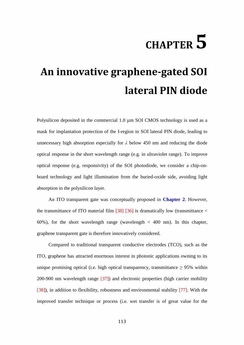
113
CHAPTER 5
An innovative graphene-gated SOI
lateral PIN diode
Polysilicon deposited in the commercial 1.0 µm SOI CMOS technology is used as a
mask for implantation protection of the I-region in SOI lateral PIN diode, leading to
unnecessary high absorption especially for λ below 450 nm and reducing the diode
optical response in the short wavelength range (e.g. in ultraviolet range). To improve
optical response (e.g. responsivity) of the SOI photodiode, we consider a chip-on-
board technology and light illumination from the buried-oxide side, avoiding light
absorption in the polysilicon layer.
An ITO transparent gate was conceptually proposed in Chapter 2. However,
the transmittance of ITO material film [38] [36] is dramatically low (transmittance <
60%), for the short wavelength range (wavelength < 400 nm). In this chapter,
graphene transparent gate is therefore innovatively considered.
Compared to traditional transparent conductive electrodes (TCO), such as the
ITO, graphene has attracted enormous interest in photonic applications owning to its
unique promising optical (i.e. high optical transparency, transmittance ≥ 95% within
200-900 nm wavelength range [37]) and electronic properties (high carrier mobility
[38]), in addition to flexibility, robustness and environmental stability [77]. With the
improved transfer technique or process (i.e. wet transfer is of great value for the

114
fabrication of electronic device) [37] [77] [78], nowadays, graphene has demonstrated
its great potentialities and applications in photonics and optoelectronics (e.g. LED,
solar cell, photodetector, laser [37]).
In this research, on the basis of its high transmittance within the 200-900nm
wavelength range and excellent conductivity, we implement monolayer graphene (i.e.
thickness of the monolayer graphene is ~ 0.345 nm) as a transparent conductive
electrode on back buried oxide (BOX), to experimentally fabricate an innovative
graphene gate on SOI lateral PIN photodiode. In the meantime, a membrane SOI
lateral PIN photodiode without graphene will be fabricated and tested for the
comparison.
5.1 Device fabrication process
The fabrication process is based on the die as presented in Figure 3.3, which was used
for the experimental characterization in the previous chapters. The process consists of
three main steps: silicon substrate etch, graphene transfer and PCB assembling (i.e.
chip on board), which will be separately presented in the next subsections.
5.1.1 XeF2 silicon substrate etch
Isotropic etching with xenon difluoride (XeF2) of silicon [79] is an ideal solution for
releasing microelectromechanical systems (MEMS) devices. MEMS get more
complicated as they contain components made from multiple or non-standard
materials (e.g. silicon dioxide, silicon nitride, polymers, plus most metals and
dielectrics, etc). There is no other isotropic etch of Si that is selective to so many
materials. The XeF2 etch provides numerous unique advantages and capabilities
compared to other wet and plasma (SF6) etch options [80]: 1) high selectivity, for
example, silicon dioxide is used as a very popular mask material with Si (oxide

115
selectivity of > 1000:1); 2) elimination of stiction, as XeF2 is a dry vapor etchant
(with Si, the etching process is 2XeF2 + Si → 2Xe + SiF4), avoiding stiction issues
which is often associated with wet etch process; 3) long undercuts, XeF2 can be used
to make very long undercuts with little or no degradation of etch stop, mask or device
layers; 4) etching through small holes (as small as 25 nm in diameter) and tight spaces.
Moreover, XeF2 does not attack polymers or other organic films, as a result,
Gel-Pak [81] can be used as carrier for ensuring safe device holding and supporting
during the process steps. Only the Gel material layer (with thickness of ~0.2 mm) is
used in this device fabrication process and detached from the Gel-Film product. As
the cross section depicted in Figure 5.1(a) shows, the Gel layer is placed on one piece
of quartz (2.5 cm 2.5 cm). The device sample (in Figure 3.4, with size of 1.8 mm
1.8 mm.) is transferred afterwards and placed upside down on the Gel layer surface,
with a slight gentle press to make sure all the edges of the sample stick on the surface
of the Gel.
The XeF2 etch process is then carried out at gas pressure of 3.8 torr, providing a
controlled, stiction-free and residue-free etching. Around 9-11 cycles (it is dependent
on each sample) is needed to completely etch the ~ 375 µm-thick silicon substrate
(listed in Table I and presented in Figure 3.1), with etch time of 180 seconds for one
cycle. Figure 5.1(b) presents the cross-section view, after the XeF2 etch, where the
released die is ~ 5 µm-thick (i.e. ultra-thin). Correspondingly, Figure 5.1(c) shows the
view of the transparent die on the Gel-quartz under optical microscope, with a good
flatness due to high selectivity of the buried oxide:Si etch. Based on the ultra-thin die
in Figure 5.1(c), a membrane SOI lateral PIN diode without graphene can be
fabricated, directly followed by the PCB assembling step in Chapter 5.1.3, i.e. device
chip-on-board technology. On the other hand, based on the flat surface of the released

116
die, graphene can be transferred onto the BOX side. An ultra-thin SOI lateral PIN
photodiode with graphene can be experimentally fabricated.
Figure 5.1- Cross-section views of flip-chip sample placed on Gel-pak layer over the quartz
piece (a), after the silicon substrate etch (b), optical view (i.e. from BOX side) of a released,
transparent die on Gel-quartz stack (c).

117
5.1.2 Graphene transfer process
Graphene transfer on BOX is implemented to experimentally fabricate the graphene-
gated SOI lateral PIN diode, which is compatible with the CMOS technology and the
graphene transfer process.
Wet transfer technique has been developed and demonstrated to achieve reliable
and reproducible transfer of large-area monolayer graphene onto arbitrary substrate
(e.g. flat substrate [82] [78]) for most practical applications. The improved transfer
provided a sheet resistance of 2.1 kΩ/sq for monolayer graphene films with a
transmittance of 97.4% in [77]. The large-area uniform monolayer graphene (most
time it is polycrystalline) is controllably grown on copper foils, by chemical vapor
deposition (CVD) [83]. Poly(methyl methacrylate) (PMMA) is widely used to transfer
CVD-grown graphene to target substrate, since it has been used as a carrier material
for transferring carbon nanotubes and mechanically exfoliated graphene flakes.
It has been reported that graphene films tend to break at the last PMMA removal
step [82]. When transferred from water to the target flat substrate, the
PMMA/graphene stack may not make full contact with the SiO2/Si substrate, and the
unattached regions tend to break and form cracks that remain when the PMMA film is
dissolved away. To improve the contact between the PMMA/graphene stack and the
substrate, after one-night natural dry in the clean room (to dry the deionized (DI)
water thoroughly), the sample is baked at ~ 160 °C for 60 minutes. The improvement
is most notable for the large-area gaps. Both acetone and acetic acid can next be used
to dissolve PMMA [84]. As acetone attacks the metal (e.g. copper wire on the PCB
board, and aluminum pad on the device sample), pure acetic acid is used to remove
the PMMA coating layer in this process.

118
Figure 5.2- Graphene (~ 3.9 mm 5.5 mm) transferred on a SiO2/Si substrate wafer with 100
nm-thick oxide layer, under optical microscope (a); cross-section view (b); under SEM (c);
and electrical current-voltage characteristics of the graphene sheet (d).
Before transferring graphene on the targeted substrate (i.e. the released die in
Figure 5.1), graphene piece is firstly transferred on the SiO2/Si wafer to evaluate the
quality, uniformity and the Epo-Tek/graphene electrical contact. The Epo-Tek [85] is
a single component, an electrically conductive modified polyimide, silver-filled
adhesive designed specifically for chip bonding in microelectronic and optoelectronic
applications.
Optical microscopy of the graphene piece (~ 3.9 mm 5.5 mm) transferred on
100 nm-thick SiO2 is presented in Figure 5.2(a), with Epo-Tek placed on the corners.
The 2-D cross section is depicted in Figure 5.2(b). Scanning electron microscopy
(SEM) view is presented in Figure 5.2(c), showing cracks and tears that have occurred
to the graphene monolayer. However, some zones also show incompletely grown
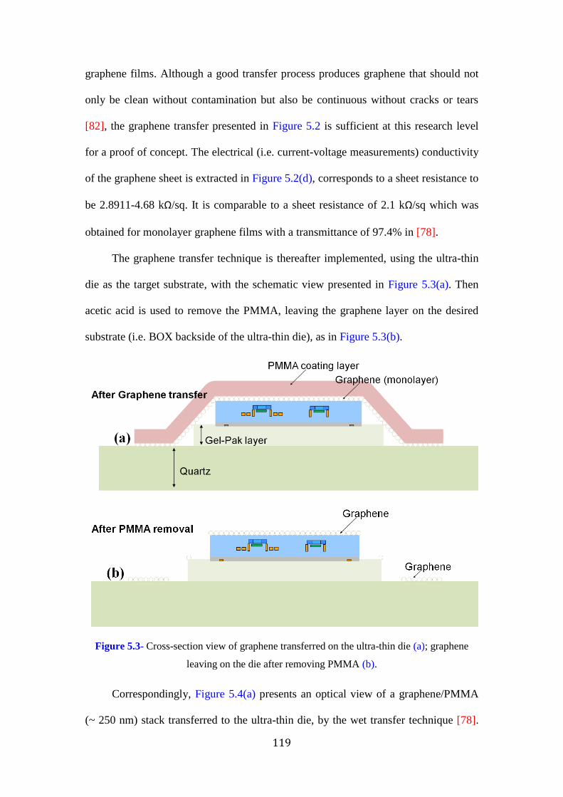
119
graphene films. Although a good transfer process produces graphene that should not
only be clean without contamination but also be continuous without cracks or tears
[82], the graphene transfer presented in Figure 5.2 is sufficient at this research level
for a proof of concept. The electrical (i.e. current-voltage measurements) conductivity
of the graphene sheet is extracted in Figure 5.2(d), corresponds to a sheet resistance to
be 2.8911-4.68 kΩ/sq. It is comparable to a sheet resistance of 2.1 kΩ/sq which was
obtained for monolayer graphene films with a transmittance of 97.4% in [78].
The graphene transfer technique is thereafter implemented, using the ultra-thin
die as the target substrate, with the schematic view presented in Figure 5.3(a). Then
acetic acid is used to remove the PMMA, leaving the graphene layer on the desired
substrate (i.e. BOX backside of the ultra-thin die), as in Figure 5.3(b).
Figure 5.3- Cross-section view of graphene transferred on the ultra-thin die (a); graphene
leaving on the die after removing PMMA (b).
Correspondingly, Figure 5.4(a) presents an optical view of a graphene/PMMA
(~ 250 nm) stack transferred to the ultra-thin die, by the wet transfer technique [78].

120
After removing the PMMA by acetic acid, the graphene layer on the die under SEM is
presented in Figure 5.4(b). A good continuity (i.e. the 'bright' conductive layer under
SEM) is observed in the graphene monolayer, but with some remaining and thin parts
(i.e. the 'black' residue part) of PMMA.
Figure 5.4- Graphene on ultra-thin die: before PMMA removal under optical microscopy (a);
after PMMA removal and under SEM (b).

121
Figure 5.5 shows the Raman spectra of graphene that had been transferred on
the SiO2/Si substrate (in Figure 5.2) and the BOX backside of the ultra-thin die (in
Figure 5.4). The Raman spectra exhibit the first-order bond stretching G band
centered at ~ 1580 cm-1
, and the two-phonon 2D band centered at ~ 2700 cm-1
[84].
Both spectra are characteristics of single layer graphene in Figure 5.5(a). In Figure
5.5(b), the G and 2D bands maps clearly show the presence of more than one layer in
the flakes. It is also important to note that the absence of the disorder-induced D band
in Figure 5.5(a) and (b) which indicates neither transfer process damages the sp2
bonds of the graphene flakes.
Figure 5.5- Raman spectra of graphene on the SiO2/Si wafer (a); graphene on the BOX
backside of the ultra-thin die (b).
5.1.3 Chip-on-board technology
The bare and ultra-thin (~ 5 µm) die with or without graphene transfer on backside
needs to be assembled on a PCB with a hole for backside illumination (Figure 5.6).

122
The die is fixed and bonded to the board, with conductive epoxy (i.e. Epo-Tek [85])
poured over its side to glue it to the board. The Epo-Tek is also used to connect
graphene as the back gate for the graphene-gated diode. The contact between the Epo-
Tek and the graphene has been firstly characterized and validated in Figure 5.2.
Figure 5.6- Two dimension (2-D) chip-on-board diagram (not to scale) for the ultra-thin die,
without graphene (a) and with graphene (b).
The chip-on-board design and technology for the ultra-thin SOI lateral PIN
diode with and without graphene are presented in Figure 5.6(a) and (b), respectively.
The light is shined from the backside via the hole of the PCB board.

123
5.2 Electrical characterization in dark condition
Under reverse and forward biases, device characterization in dark condition is
performed in the devices with and without graphene transfer, before and after process,
to verify device robustness to post-processing steps.
Figure 5.7- Dark current performances under reverse and forward biases in single on-
substrate (S5) and on-membrane (M20) diodes (Li = 5 and 20 µm) with and without graphene
transfer, before and after process.
Device performance in the dark condition are plotted in Figure 5.7. After the
full process, the diode reverse leakage currents are reduced and the diode ideality

124
factor at forward bias (M20 in Figure 5.7) is getting close to 1. The improvement is
mainly related to the annealing used during the fabrication process, i.e. a low-
temperature heating at ~ 120 °C for 8 hours to completely cure the Epo-Tek for wire
bonding.
While comparing the local annealing that was carried out in Chapter 3, the
annealing effect on the diode leakage currents in Chapter 3 and Chapter 5 are
similar. Therefore, the low-temperature annealing and its effect can be qualitatively
interpreted by the Arrhenius law. To the first order, Arrhenius law can be expressed as
[86] [87] : where ka is the rate constant of the reaction in
annealing, and Ea is the activation energy for the annealing process, in unit of eV.
Arrhenius' equation gives the dependence of the rate constant on the absolute
temperature, i.e. higher temperature induces faster reactions. As in [87], the activation
energies of Si can be varied from 0.08 to 0.5 eV in the annealing process, which
would result in a multiple of 2-44 for the rate constant between 250 °C and 120 °C.
Therefore, the annealing effect on the diode leakage current could be qualitatively
comparable for a relatively high-temperature annealing at 250 °C with 30 minutes
local heating (in Chapter 3) and a lower-temperature annealing at 120 °C with a
longer heating time of 8 hours (in Chapter 5).
SOI lateral PIN diodes lying on substrate, which did not suffer from the
membrane etch (DRIE), are not degraded after the XeF2 etch and the graphene
transfer processes. And the reverse and forward characteristics of the on-membrane
diodes now get close to the characteristics of the on-substrate diode, after the process
and annealing.

125
5.3 Device optical response
Consistent with the measurement set-up described in Figure 2.10, i.e. the
monochromator illumination system and the semiconductor parameter analyzer, the
chip-on-board technology and the backside illumination are implemented in this
experiment in Figure 5.8, to avoid the absorption in the top polysilicon layer. The
incident wavelengths are selected in the ultraviolet (UV) and the visible (VS)
wavelength ranges (i.e. 200-900 nm), with the power densities on the level of 10-6
-10-
4 W/cm
2.
Figure 5.8- Chip-on-board and backside illumination system.
5.3.1 In the visible (VS) wavelength range
Responsivities of the ultra-thin SOI lateral PIN photodiodes with and without
graphene transfer are extracted by equation (4.8), under a reverse bias of 2.0 V.
Responsivities in the visible (VS) wavelength range (within 450-900 nm) are
presented in Figure 5.9.

126
In the photodiodes (Li = 5 µm) with (where gate bias is 0 V) and without
graphene, the responsivities are almost the same, no obvious decrease or degradation
is observed within the whole VS wavelength range. It demonstrates the high optical
transparency of graphene (i.e. transmittance is over 95%) within 200-900 nm
wavelength range, as discussed in [37]. Slight variation in responsivity between the
two devices could be due to the device variation. The responsivities increase with the
intrinsic length (Li = 5 and 20 µm), as discussed in Chapter 4, due to the increased
percentage of device photosensitive area. Peak responsivities in the device with Li =
20 µm are observed at ~ 490, 590 and 760 nm with ~ 0.11, 0.08 and 0.04 A/W.
Large improvement of responsivity is therefore achieved for wavelength below
600 nm in these ultra-thin SOI lateral PIN photodiodes (e.g. Li = 20 µm) under the
backside illumination, while compared to the responsivities of the SOI lateral PIN
diodes with substrate in Figure 4.7(a), e.g. responsivity of 0.03 A/W at 590 nm. Large
optical absorption observed in the polysilicon under the topside illumination
suppressed the device optical response in Figure 4.7(a).

127
Figure 5.9- Experimental responsivities within the visible (VS) wavelength range, in the
ultra-thin SOI lateral PIN diodes (Li = 5 and 20 µm) with and without graphene transfer, at
reverse bias 2.0 V and under backside illumination.
5.3.2 In the ultraviolet (UV) wavelength range
The responsivities in the ultraviolet (UV) wavelength range are presented in Figure
5.10. In the device with Li = 20 µm, the best responsivity is obtained at 390 nm, with
0.18 A/W. Peak responsivities are also achieved with ~ 0.15, 0.17 and 0.14 A/W,
respectively at 440, 400 and 340 nm wavelengths. These are comparable with or even
better than the most representative results in [9], i.e. responsivities achieved 0.18 and
0.1 A/W respectively at 400 and 480 nm wavelengths, by using an ARC coating layer
for the optical optimization of absorption in the SOI lateral PIN photodiode.
For the wavelength below 250 nm, the device responsivities are relatively low,
especially in the device with Li = 5 µm. Partially, it could be due to the limited
incident power density (~ 10-6
W/cm2) which results in the device low output
photocurrent (the dark current is close to the photocurrent) and therefore large
measurement error. On the other side, light penetration depth in silicon is short under
the short-wavelength illumination, as described in Figure 1.5. The light penetration
depth in the 200-250 nm wavelength range is merely ~ 6 nm. Photo-generated carriers
mainly occur around the silicon surface region, recombination velocity at or around
the surface will therefore lead to the decrease of the device output optical response.
Light reflection needs to be taken into account where the 1.0 µm-thick BOX layer is
the top layer of the photodiode under illumination. Optical simulation is needed to
analyze and interpret the optical response.
128
Figure 5.10- Experimental responsivities within the ultraviolet (UV) wavelength range, in the
ultra-thin SOI lateral PIN diodes (Li = 5 and 20 µm) with and without graphene transfer, at
reverse bias 2.0 V.
5.3.3 Simulation analysis in absorption
The optical simulation is performed in Atlas/SILVACO [40], to analyze the device
optical response obtained in Figure 5.9 and Figure 5.10. Based on the ultra-thin die
(without graphene) investigated in this chapter, the multilayer stack is:
Si3N4/SiO2/Polysilicon/SiO2/Silicon/BOX, and light is perpendicularly illuminated
from the BOX side (i.e. backside illumination). Effective light absorption (i.e. the
available photocurrent in the I-region over the total source photocurrent) is extracted
for single wavelength within 200-900nm.
Detailed results of absorption averaged (with bandwidth Δλ = 10 nm) for each 4
nm wavelength increment are presented in Figure 5.11(a) for the VS wavelength
range 450-900 nm and in Figure 5.11(b) for the UV wavelength range 200-450 nm.
The ‘series 1’ and ‘series 2’ light absorption of the ultra-thin SOI lateral PIN diode
(with Li = 10 µm) in Figure 5.11, are simulated with the two-series material

129
thicknesses which were specifically implemented for the simulations in Figure 4.5 and
Figure 4.3 (a), respectively.
Peak responsivities observed at ~ 490, 590 and 760 nm wavelengths in
experiments correspond to the absorption peaks in the two-series simulations in
Figure 5.11(a) within the 450-900 nm wavelength range. Moreover, the effective
absorption exceeds 0.4 at ~ 450 nm and qualitatively validates the optical simulation
presented in Figure 4.7 (c), where the top polysilicon layer was replaced by an ARC
layer and the diode with black silicon reflector obtained the effective absorption of 0.3
at ~ 450 nm wavelength.
Figure 5.11- Light absorption average (over Δλ of 10 nm) of the ultra-thin SOI lateral PIN
diode (Li = 10 µm) in the visible wavelength range (a) and ultraviolet wavelength range (b),

130
taking the two-series material thicknesses implemented into the simulaitons of Figure 4.5 and
Figure 4.3(a) (respectively indicating as series 1 and series 2).
The maximum responsivity obtained at 390 nm is also confirmed by the ‘series
1’ simulation in Figure 5.11(b), where the highest absorption is observed at ~390 nm
wavelength and shifted by ~ 20 nm in ‘series 2’. The remaining quantitative
deviations including slight shifts in the peaks and valleys between the two-series
simulations in Figure 5.11(b) result from the exact material thicknesses implemented
into the two-series simulations.
Within wavelength range 300-400 nm, upward trend in the experimental
responsivity (Figure 5.10) has been primarily confirmed by the absorption simulation
in Figure 5.11(b). Another observation is that relatively stable and high absorption
(0.25-0.3) is simulated within the 200-250 nm wavelength range in the device (Li = 10
µm), though 1.5-2 × lower than main peak at 390 nm, that confirms the surface
recombination in the ultra-thin photodiode.
5.3.4 Under graphene-gate bias
A primary demonstration of the graphene gate control is done on the die level, where
an ultra-thin SOI lateral PIN photodiode (Li = 5 µm) with graphene transferred on
BOX backside is measured in probe station. The backside of the whole photodiode is
partially covered by Epo-Tek, which is used as the conductive glue to fix the die on
the PCB board and connect the graphene layer as gate electrode.
Under topside illumination (i.e. white light illuminated from the top Si3N4 side),
the device output photocurrent versus gate voltage is presented in Figure 5.12, at
reverse bias 1.0 and 2.0 V. As discussed in Chapter 2, the gate bias can alter the
depletion condition in the I-region of the photodiode, the output photocurrent reach a
‘maximum plateau’ level in Figure 5.12 under fully-depleted condition (e.g. gate

131
voltage > 60 V). The shift in gate voltage (i.e. from 40 V to 60 V) that alters the I-
region from accumulation to full depletion in the current-voltage (gate) characteristics
of Figure 5.12, is quite close to the gate voltage shift ~ 20 V in Figure 3.14(b) with the
Al gate electrode, which validates the gate control achieved from the graphene
conductive layer. The shift in the whole current-voltage curves in Figure 5.10,
compared to the output characteristics in Figure 3.14(b), is due to the fixed oxide
charges, which has been discussed in Chapter 3. Generally, the output optical
response of the ultra-thin photodiode is optimized by the graphene-gate bias.
Figure 5.12- Device output photocurrent versus gate voltage, in the ultra-thin SOI lateral PIN
diodes (Li = 5 µm) with graphene transferred on BOX side, at reverse biases 1.0, 2.0 V and
under topside illumination

132
5.4 Summary
In this chapter, an innovative ultra-thin SOI lateral PIN diode has been experimentally
fabricated, with XeF2 thinning, graphene transfer and chip-on-board assembling.
Device degradation is obviously not induced by the fabrication process.
The optical response obtained in the ultra-thin photodiode with and without
graphene is almost the same within the 200-900 nm wavelength range, which
validates the high transmittance of graphene (without gating). Maximum responsivity
of 0.18 A/W is obtained at 390 nm wavelength in the photodiode with Li = 20 µm.
Large improvement of responsivity is achieved for wavelength below 600 nm, in
comparison with the optical response discussed in Chapter 4 for the SOI lateral PIN
photodiode with polysilicon mask and substrate or black silicon backside reflectors. A
graphene-gate control has also been primarily demonstrated for the optimization of
device output optical response. With applied gate biasing, the depletion condition of
the I-region can be altered and reach the FD condition, maximizing the diode output
photocurrent as expected.
With optimized device performance, this ultra-thin photodiode has potential
applications in UV and RGB sensing systems.
133
CHAPTER 6
Summary and perspectives
6.1 Summary
This thesis work has investigated an optical sensor, i.e. a SOI lateral PIN diode.
Under standard SOI technology (silicon film thickness > 100 nm), the intrinsic
region in the lateral PIN diode is not fully depleted. A top ITO-gated photodiode has
been conceptually proposed and theoretically analyzed, with two-dimensional device
modeling and simulation. Another back Al-gated photodiode has been fabricated and
characterized mainly for experimental validation of device performance optimization.
Gate bias alters the depletion condition of the intrinsic region. Under fully depleted
condition, the maximum optical response (e.g. close to 100% of QI in the ITO-gated
photodiode or responsivity in the Al-gated photodiode) has been achieved in the ITO-
gated and Al-gated photodiodes.
A low-temperature annealing (~ 250 °C temperature and 30 minutes heating)
has been performed using the micro-heater (and the diode as thermal sensor) to
stabilize the PIN diode electrical characteristics. Device recovery and performance
improvement have been observed in the suspended diode after degraded by the
MEMS post-processing (DRIE and Al deposition), mainly considering the G-R
current under forward bias, low-frequency noise characteristics, and the diode reverse
leakage current. By two-dimensional device simulation, we have demonstrated that

134
theses performance are related to trap neutralization and improvement of carriers’
lifetime.
Four different backside reflectors (i.e. gold, aluminum, substrate and black
silicon) have been used and placed below the SOI lateral PIN diodes, varied the light
absorption in the intrinsic region and therefore modulated the device optical response.
Responsivities or responsivity peaks (e.g. at 490, 590, and 760 nm wavelengths) are
specifically obtained in the photodiodes with different backside reflectors (e.g. with
Al backside reflector). Optical sensing capability has been advanced within 450-900
nm wavelength range, where the multiple-wavelength detection (e.g. 462, 486, 536,
550, 566, 586, 602, 620, 742, 760 and 794 nm wavelengths) is consequently achieved
by combining the mathematic ratios among the 4 specific out photocurrent or
responsivity under same illumination.
An ultra-thin-die SOI lateral PIN diode has been experimentally fabricated and
measured, with and without graphene top-gate transfer. High optical response within
200-450 nm and a further improvement of device responsivity within 450-900 nm
wavelength ranges have been achieved in the two types of photodiodes. Excellent
transmittance and electrical gate control have been demonstrated in the graphene-
gated photodiode.
At the end of the thesis, we can establish a final quantitative comparison of our
best results (in the lateral PIN diode with Li = 20 µm) versus the state-of-the-art: in
the VS wavelength range, the SOI lateral PIN photodiode with Al backside reflector
achieves peak responsivities for 3 different wavelengths (490, 590 and 760 nm)
respectively of 0.07, 0.1, 0.05 A/W. The maximum responsivity of 0.1 A/W at 590 nm
is ~ 2 higher than the resonant and most representative responsivity of 0.05 A/W in

135
the photodiode with the same intrinsic length in literature [24]; in the UV wavelength
range, the highest responsivity achieved in the ultra-thin diode with Li = 20 µm is 0.18
A/W at 390 nm wavelength. Peak responsivities are also achieved with ~ 0.15, 0.17
and 0.14 A/W, respectively at 440, 400 and 340 nm wavelengths. These are
comparable with or even better than the state-of-the-art [9], i.e. responsivities
achieved 0.18 and 0.1 A/W respectively at 400 and 480 nm wavelengths, by using an
ARC coating layer for the optical optimization of absorption in the SOI lateral PIN
photodiode.
6.2 Perspectives
Based on the research results presented in this thesis, several issues are recommended
to be solved in future work:
1) Optimization in the device structure: based on the numerical simulation and
experimental characterization in this thesis, the top or back gate bias is applied to the
SOI lateral PIN diode, achieving the full depletion condition in the I-region and
maximizing the device output photocurrent, QI and device responsivity. However,
when the intrinsic length exceeds the carrier diffusion length, there exists a decrease
in the device optical response due to the carrier recombination. An optimization in the
device intrinsic length needs to be done next, considering the detailed electrical
parameters. Moreover, as for the top-side and bottom-side illumination systems
illustrated in this thesis, to find out the optimal solution for the photodiode is also
highly needed.
2) Light filtering with polysilicon layer: as large absorption was observed in the
polysilicon layer which was used for the implantation protection in the device
fabrication technology, one point can be taken into account for the next work or future

136
design of optical sensor is that: using polysilicon layer (with varied thickness) as one
specific optical layer to filter the unwanted incident light wavelengths or combined
with backside reflectors to enhance the optical response for the specific and precise
wavelength detection.
3) Further investigation in local annealing: the local annealing is operated in this
thesis at a temperature ~ 250 °C, showing its high interest and advantage in device
performance optimization and improvement. However, annealing at a higher
temperature (e.g. 300 °C, 350 °C) or even a standard annealing at 430 °C with the
forming gas in experiments, did not work for the device improvement. An aluminum
adhesion problem on the buried oxide layer was observed (probably due to surface
texture) and the diode reverse leakage current characteristics turned to be hard to
interpret afterwards. Further investigation and explanation of the local annealing
operation and concept need to be done in further work.
4) Deep investigation in diode forward characteristics: in the diode forward
current-voltage characteristics as presented in Figure 3.10, different mechanisms are
dominating respectively, under the varied back-gate bias (e.g. -60, 0, 90 V) altering
the depletion condition in the I-region from the accumulation, to full depletion and
inversion. The physical insight into the carrier lifetime, interface trap status, and the
depletion condition of the I-region which are related to the diode forward
characteristics need to a deeper investigation.
5) Graphene implementation: a SOI lateral PIN diode with graphene has been
experimentally fabricated in this thesis, with first validation of the excellent optical
transparency and good electrical conductivity. How to improve and optimize the
graphene transfer (e.g. a graphene transfer without cracks or tears) and

137
implementation in the SOI lateral PIN diode or other optical sensor is the further work
that needs to be done and strongly investigated.
6) Application in the Internet-of-Things: Internet-of-Things (IoT) is the current and
most important field for the sensor applications. Based on the multiple-wavelength
detection capability of the photodiode with different backside reflectors, how to apply
this design or the idea for optical sensing in IoT is worth taking into account for the
future application requiring innovative, highly miniaturized and low power solutions.
7) UV and RGB sensing: based on the high optical response obtained in the ultra-
thin photodiode (in the ultraviolet UV and visible VS wavelength ranges) and the
backside reflectors application for the multiple-wavelength detection within the VS
range, for the next research, we can implement the ultra-thin photodiode together with
backside reflectors to advance the optical sensing capability and achieve the multi-
wavelength detection in the whole UV and VS ranges (e.g. red-green-blue sensing).
8) A self-powered system with PN junctions: similar to the structure of the lateral
PIN photodiode, photovoltaic cell is also based on the PN junction. How to
implement photovoltaic cell with the photodiode in one chip and to construct a self-
powered system with the PN junctions is one issue that can be extended for this
research, for a portable, compact and more environment-friendly system.
9) Strain effect on diode properties: the silicon device, i.e. the SOI lateral PIN diode,
can unavoidably be strained after the MEMS processing (i.e. DRIE, Al deposition,
XeF2 Si substrate etch and ultra-thin die transfer). However, as investigated in
literature, the resistivity, length and transverse width of the silicon material, and
mobility are changed while the silicon device is strained. Therefore, the reverse and
forward characteristics of the on-membrane diode or all the diodes on the thinned die

138
need a further investigation with respect to strain, compared to the on-substrate diode
without MEMS processing.

139
Bibliography
[1] Peter Y. Yu, Manuel Cardona, Fundamentals of Semiconductors, Physics and
Materials Properties, 4th ed., Springer-Verlag Berlin Heidelberg, 2010, pp. 243–245.
[2] S.M. Sze, K.K. Ng, Physics of Semiconductor Devices, 3rd ed., U.S.: Wiley
Interscience, 2007, pp. 213–684.
[3] 刘恩科, 朱秉升, 罗晋生 编著, 半导体物理学, 第七版, 电子工业出版社, 北京,
2008, pp. 317–320.
[4] J. P. Colinge, C. A. Colinge, Physics of Semiconductor Devices, Kluwer
Academic Publishers, 2002, pp. 74–145.
[5] Donald A. Neamen, Semiconductor Physics and Devices Basic Principles, 3rd ed.
McGraw-Hill Companies, Inc., 2003, pp. 192–246.
[6] Website [online]: http://pveducation.org/pvcdrom/types-of-recombination
[7] Umesh K. Mishra, Jasprit Singh, Semiconductor Device Physics and Design,
Springer, Netherlands, 2008, pp. 146–177.
[8] A. Afzalian, D. Flandre, “Physical modeling and design of thin-film SOI lateral
PIN photodiodes,” IEEE Transactions on Electron Devices, vol. 52, no. 6, pp. 1116–
1122, 2005.
[9] O. Bulteel, “Silicon-on-Insulator optoelectronic components for micropower solar
energy harvesting and bio-environmental instrumentation,” Ph.D. dissertation,
ICTEAM Institute, Université Catholique de Louvain, Louvain-la-Neuve, Belgium,
2011.
[10] A. D. Luca, F. Udrea, et al., Semiconductor Devices in Harsh Conditions, CRC
Press, U.S., 2016, pp. 87–106.
[11] S. Santra, F. Udrea, P. K. Guha, S. Z. Ali, I. Haneef, “Ultra-high temperature ( >
300 ˚C) suspended thermodiode in SOI CMOS technology”, Microelectronics Journal,
vol. 41, pp. 540–546, 2010.

140
[12] O. Bulteel, A. Afzalian, D. Flandre, “Fully integrated blue/UV SOI CMOS
photosensor for biomedical and environmental applications”, Analog Integrated
Circuits and Signal Processing, vol. 65, no.3, pp. 399–405, 2010.
[13] L. Arias, S. Torres, D. Sbarbaro, O. Farias, “Photodiode-based sensor for flame
sensing and combustion-process monitoring”, Applied Optics, vol. 47, no.29, pp.
5541–5548, 2008.
[14] Website [online]: XFAB-https://www.xfab.com/en/technology/cmos/10-um-
xc10/
[15] Website [online]: XFAB-https://www.xfab.com/en/technology/soi/10-um-xi10/
[16] N. Ren, Z. Liu, Q. Wang, “Investigating the effects of microstructure on optical
properties of different kinds of polysilicon thin films”, Physics Letters A, vol. 379, pp.
1153–1160, 2015.
[17] A. Gorin, A. Jaouad, E. Grondin, V. Aimez, P. Charette, “Fabrication of silicon
nitride waveguides for visible-light using PECVD: a study of the effect of plasma
frequency on optical properties,” Optics Express, vol. 16, no. 18, pp. 13509–13516,
2008.
[18] W. Matthew, C. Ning, “Deep reactive ion etch condition recipe”, Proceedings of
the SPIE, vol. 5342, pp. 103–110, 2004.
[19] A. A. Ayon, R. L. Bayt, K. S. Breuer, “Deep reactive ion etching: a promising
technology for micro- and nanstatellites”, Smart Materials and Structures, vol. 10, pp.
1135–1144, 2001.
[20] A. A. Ayon, K. S. Chen, K. A. Lohner, S. Spearing, “Deep Reactive Ion Etching
of Silicon”, Mat. Res. Soc. Symp. Pro., vol. 546, pp. 51–61, 1999.
[21] Website [online]: https://en.wikipedia.org/wiki/Deep_reactive-
ion_etching#Bosch_process
[22] “The Bosch Process for Etching Micro-Mechanical Systems (MEMS) -
Principles, Advances and Applications by Oxford Instruments Plasma”, Nov. 26 2010,
Sponsored by Oxford Instruments Plasma Technology.

141
[23] A. Ono, Y. Matsuo, H. Satoh, H. Inokawa, “Sensitivity improvement of silicon-
on-insulator photodiode by gold nanoparticles with substrate bias control”, Applied
Physics Letters, vol. 99, 062105, 2011.
[24] V.S. Sinnis, M. Seto, G.W. Hooft, Y. Watabe, A.P. Morrison, W.Hoekstra, W.B.
Boer, “Silicon-based resonant-cavity-enhanced photodiode with a buried SiO2
reflector”, Applied Physics Letters, vol. 74, no. 9, pp. 1203–1205, 1999.
[25] B. W. Cheng, C. B. Li, F. Yao, C. L. Xue, J. G. Zhang, R. W. Mao, Y. H. Zuo,
“Silicon membrane resonant-cavity-enhanced photodetector”, Applied Physics Letters,
vol. 87, 06111, 2005.
[26] D. Ivnitski, I. Abdel-Hamid, P. Atanasov, E. Wilkins, “Biosensors for detection
of pathogenic bacteria”, Biosensors & Bioelectronics, vol. 14, pp. 599–624, 1999.
[27] P. H. Ruane, R. Edrich, D. Gampp, S. D. Keil, R. L. Leonard, and R. P. Goodrich,
“Photochemical inactivation of selected viruses and bacteria in platelet concentrates
using riboflavin and light”, Transfusion, vol. 44, no. 6, pp. 877–885, 2004.
[28] N. J. Joh, K. Boon, K. Y. Leong, “Use color sensors for precise measurement”, in
Electronic Engineering Times-Asia, Dec. 16-31, 2006.
[29] Intersil [ISL29125, FN8424.2], “Digital Red, Green and Blue Color Light Sensor
with IR Blocking Filter”, California, U.S., Jan. 24, 2014. [Online] Available:
http://www.intersil.com/en/products/optoelectronics.html
[30] X. Wang, O. S. Wolfbeis, “Optical methods for sensing and imaging oxygen:
materials, spectroscopies and applications”, Chem. Soc. Rev., vol. 43, pp. 3666–3761,
2014.
[31] H. M. Anderson, M. P. Splichal, “An integrated system of optical sensors for
plasma monitoring and plasma process control”, in Proc. SPIE 2091, Microelectronic
Processes, Sensors, and Controls, 333, Feb. 15, 1994.
[32] Y. Mattley, “Plasma Monitoring with Miniature High-Resolution Spectroscopy”,
Florida, U.S., Apr. 10, 2014. [Online] Available: http://oceanoptics.com.
[33] E. Schmachtenberg, A. Hegenbart, “Monitoring of plasma processes by OES”,
Vacuum’s Best VIP, vol. 19, pp. 39–43, 2007.

142
[34] T. Rudenko, A. Rudenko, V. Kilchytska, S. Cristoloveanu, T. Ernst, J. P. Colinge,
V. Dessard, D. Flandre, “Determination of film and surface recombination in thin-film
SOI devices using gated-diode technique”, Solid-State Electronics, vol. 48, pp. 389–
399, 2004.
[35] J.P. Colinge, Silicon-on-insulator technology: Material to VLSI, 2nd edition,
Kluwer Academic Publishers, 1997, pp. 123–185.
[36] T. Kawashima, H. Matsui, N. Tanabe, “New transparent conductive films: FTO
coated ITO”, Thin solid films, vol. 445, pp. 241–244, 2003.
[37] F. Bonaccorso, Z. Sun, T. Hasan and A. C. Ferrari, “Graphene photonics and
optoelectronics”, Nature photonics, vol. 4, pp. 611–622, 2010.
[38] K. Ellmer, “Past achievements and future challenges in the development of
optically transparent electrodes”, Nature photonics, vol. 6, pp. 809–817, 2012.
[39] G. Li, Y. Zeng, W. Hu, Y. Xia, “Analysis and Simulation for Current-Voltage
Models of Thin-Film Gated SOI Lateral PIN Photodetectors”, Optik, vol. 125, no. 1,
pp. 540–544, 2014.
[40] Atlas User's Manual: Device Simulation Software, Nov. 2014, Silvaco Inc., Santa
Clara, U.S., 2016, pp. 100–696.
[41] G. Li, Y. Zeng, W. Hu, Y. Xia, W. Peng, “Modeling and Electrical Simulations
of Thin-film Gated SOI Lateral PIN Photodetectors for High Sensitivity and Speed
Performances”, 17th CCF Conference, NCCET 2013, Xining, China, July 20-22, 2013,
CCIS 396, pp. 235–243.
[42] G. Li, Y. Zeng, W. Zou, Y. Xia, “Operation of thin-film gated SOI lateral PIN
photodetectors with gatevoltage applied and intrinsic length variation”, Optik, vol.
125, Issue 21, pp. 6483–6487, 2014.
[43] A. Afzalian, D. Flandre, “Characterization of quanyum effciency, effective
lifetime and mobility in thin film ungated SOI lateral PIN photodiodes”, Solid State
Electronics, vol. 51, pp. 337–342, 2007.
[44] G. Li, Y. Zeng, Y. Xia, H. Xu, “Optical characteristics for thin-film gated SOI
lateral PIN photodetector (in Chinese)”, Journal of National University of Defense
Technology, vol. 37, no. 1, pp. 34–38, 2015.

143
[45] G. Li, N. André, O. Poncelet, P. Gérard, S. Z. Ali, F. Udrea, L. A. Francis, Y.
Zeng, D. Flandre, “Operation of Suspended Lateral SOI PIN Photodiode with
Aluminum Back Gate”, in Int. EUROSOI-ULIS conference, Vienna, Austria, January
25-27, 2016, pp. 155–158.
[46] E. H. Poindexter, G. J. Gerardi, M. E. Rueckel, P. J. Caplan, “Electronic traps
and Pb Centers at the Si/SiO2 interface: Band-gap energy distribution”, Journal of
Applied Physics, vol. 58, no. 10, pp. 2844–2849, 1984.
[47] D. K. Schroder, Semiconductor material and device characterization, 3rd edition,
John Wiley & Sons, Inc. , Hoboken, New Jersey, Canada, 2006, pp. 319–356.
[48] N. Dasgupta, A. DasGupta, Semiconductor devices modelling and technology,
Prentice-Hall of India, New Delhi, India, 2004, pp. 234–250.
[49] N. André, G. Li, P. Gérard, O. Poncelet, Y. Zeng, S. Z. Ali, F. Udrea, L. A.
Francis, D. Flandre, “Wide Band Study of Silicon-on-Insulator Photodiodes on
Suspended Micro-Hotplates Platforms”, in Int. Conf. on IC Design & Technology
(ICICDT) conference, Leuven, Belgium, June 1-3, 2015, pp. 1–4.
[50] Website [online]: http://www.ajaint.com/what-is-e-beam-evaporation.html
[51] K. Bordo, H. G. Rubahn, “Effect of Deposition Rate on Structure and Surface
Morphology of Thin Evaporated Al Films on Dielectrics and Semiconductors”,
Materials Science (Medziagotyra), vol. 18, no. 4, pp. 313–317, 2012.
[52] C. Novo, R. Giacomini, A. Afzalian, D. Flandre, “Operation of lateral SOI PIN
photodiodes with back-gate bias and intrinsic length variation”, in Proc. 223rd ESC
Transactions Meeting, 2013, pp. 121–126.
[53] K. Onishi, C. S. Kang, R. Choi, H. Cho, S. Gopalan, R. E. Nieh, S. A. Krishnan,
J. C. Lee, “Improvement of surface carrier mobility of HfOsub 2 MOSFETs by high-
temperature forming gas annealing”, IEEE Transactions on Electron Devices, vol. 50,
no. 2, pp. 384–390, 2003.
[54] Z. Peng, Y. Wang, H. Shen, C. Li, J. Wu, Y. Bai, K. Liu, X. Liu, “Effects of
combined NO and forming gas annealing on interfacial properties and oxide reliability
of 4H-SiC MOS structures”, Microelectronics Reliability, vol. 58, pp. 192–196, 2016.

144
[55] A. D. Luca, V. Pathirana, S. Z. Ali, F. Udrea, “Silicon on insulator thermodiode
with extremely wide working temperature range”, in 17th Int. Conf. on 2013 IEEE
Transducers & Eurosensors XXVII, Barcelona, Spain, 2013, pp. 1911–1914.
[56] C. Novo, R. Giacomini, R. Doria, A. Afzalian, D. Flandre, “Illuminated to dark
ratio improvement in lateral SOI PIN photodiodes at high temperatures”,
Semiconductor Science and Technology, vol. 29, 075008, 2014.
[57] I. Aberg, B. Ackland, J. V. Beach, C. Godek, R. Johnson, C. A. King, A. Lattes,
J. O’Neill, S. Pappas, T. S. Sriram, and C. S. Rafferty, “A low dark current and high
quantum efficiency monolithic germanium-on-silicon CMOS imager technology for
day and night imaging applications”, IEEE Int. Electron Devices Meet, 2010, 14.4.1.
[58] C. T. DeRose, D. C. Trotter, W. A. Zortman, A. L. Starbuck, M. Fisher, M. R.
Watts, and P. S. Davids, “Ultra-compact 45 GHz CMOS compatible Germanium
waveguide photodiode with low dark current”, Optics Express, vol. 19, no. 25, pp.
24897–24904, 2011.
[59] A. Schmidt, S. Dreiner, H. Vogt and U. Paschen, “Thin-Film SOI PIN-Diode
Leakage Current Dependence on Back-Gate-Potential and HCI Traps”, in 2015 45th
European. Conf. ESSDERC, Sep. 14-18, 2015.
[60] G Li, V. Kilchytska, N. André, L. A. Francis, Y. Zeng, D. Flandre, “Leakage
Current and Low-Frequency Noise Analysis and Reduction in a Suspended SOI
Lateral PIN Diode”, revised for IEEE Transactions on Electron Devices.
[61] J. C. Doll, B. L. Pruitt, Piezoresistor Design and Applications, Springer, New
York, 2013, pp. 21–49.
[62] C. H. Je, C. A. Choi, S. Q Lee, and W. S. Yang, “Surface Micromachined
Pressure Sensor with Internal Substrate Vacuum Cavity”, ETRI Journal, vol. 38, no. 4,
pp. 685–694, 2016.
[63] I. Aberg, O.O. Olubuyide, C.N. Chleirigh, I. Lauer, D.A. Antoniadis, J. Li, R.
Hull, J.L. Hoyt, “Electron and hole mobility enhancements in sub-10 nm-thick
strained silicon directly on insulator fabricated by a bond and etch-back technique”, in
VLSI Technology, Honolulu, USA, June 15-17, 2004, pp. 52–53.
[64] T. Rudenko, V. Kilchytska, V. Dessard, D. Flandre, “A revised reverse gated-
diode technique for determining generation parameters in thin-film silicon-on-
145
insulator devices and its application at high temperature”, Journal of Applied Physics,
vol. 97, no.093718, pp.1–9, 2005.
[65] G. Li, N. André, P. Gérard, S. Z. Ali, F. Udrea, L. A. Francis, Y. Zeng, D.
Flandre, “Multiple-Wavelength Detection in SOI Lateral PIN Diodes with Backside
Reflectors”, IEEE Transactions on Industrial Electronics, no. 99, 2017.
[66] P. R. Gray, P. J. Hurst, S. H. Lewis, R. G. Meyer, “Noise in Integrated Circuits”,
in Analysis and Design of Analog Integrated Circuits, 5th edition, WILEY, New York,
2009, pp. 736–745.
[67] M. Haartman and M. Östling, “Fundamental noise mechanisms”, in Low-
frequency noise in advanced MOS devices, Springer, Netherlands, 2007, pp. 5–15.
[68] M. J. Kirton and M. J. Uren, “Noise in solid-state microstructure: A new
perspective on individual defects, interface states and low-frequency (1/f) noise”,
Advances in Phys., vol. 38, no. 4, pp. 367–468, 1989.
[69] A. A. Balandin, “Low-frequency 1/f noise in graphene devices”, nature
nanotechnology, vol. 8, pp. 549–555, 2013.
[70] D. Macdonald, A. Cuevas, J. Wong-Leung, “Capture cross sections of the
acceptor level of iron–boron pairs in p-type silicon by injection-level dependent
lifetime measurements”, Journal of Applied Physics, vol. 89, no. 12, pp. 7932–7939,
2001.
[71] F. Udrea, J. W. Gardner, D. Setiadi, J. A. Covington, T. Dogaru, C. C. Lu, W. I.
Milne, “Design and simulations of SOI CMOS micro-hotplate gas sensors”, Sensors
and Actuators B: Chemical, vol. 78, pp. 180–190, 2001.
[72] F. L. Pedrotti, L. S. Pedrotti, Introduction to Optics, 2nd edition, Prentice-Hall
International, Inc., U.S., 1993, pp. 408–421.
[73] Eugene Hecht, Optics, 4th edition, Pearson Education, Inc., U.S., 2002, pp. 111–
126.
[74] Website: http://www.photonics.com/EDU/Handbook.aspx?AID=25501.
[75] S. Hwng, C. N. LaFratta, V. Agarwal, X. Yu, David R. Walt, and Sameer
Sonkusale, “CMOS Microelectrode Array for Electrochemical Lab-on-a-Chip
Applications”, IEEE Sensors Journal, vol. 9, no. 6, pp. 609–615, 2009.

146
[76] G. Li, N. André, O. Poncelet, P. Gérard, S. Z. Ali, F. Udrea, L. A. Francis, Y.
Zeng, D. Flandre, “Silicon-on-Insulator Photodiode on Micro-Hotplate Platform with
Improved Responsivity and High-Temperature Application”, IEEE Sensors Journal,
no. 99, pp. 3017–3024, 2016.
[77] X. Li, Y. Zhu, W. Cai, M. Borysiak, B. Han, D. Chen, R. D. Piner, L. Colombo,
R. S. Ruoff, “Transfer of large-area graphene films for high-performance transparent
conductive electrodes”, Nano Letters, vol. 9, no. 12, pp. 4359–4363, 2009.
[78] J. W. Suk, A. Kitt, C. W. Magnuson, Y. Hao, S. Ahmed, J. An, A. K. Swan, B. B.
Goldberg, R. S. Ruoff, “Transfer of CVD-grown monolayer Graphene onto arbitrary
substrate”, ACS NANO, vol. 5, no. 9, pp. 6916–6924, 2011.
[79] Website [online]: http://www.spts.com/products/xef2-release-etch.
[80] XeF2 Etch for MEMS Release [SPTS], Website [online]: www.spts.com
[81] Website [online]: http://www.gelpak.com/--wf-film.
[82] X. Liang, B. A. Sperling, I. Calizo, G. Cheng, C. A. Hacker, Q. Zhang, Y. Obeng,
K. Yan, H. Peng, Q. Li, X. Zhu, H. Yuan, A. R. Walker, Z. Liu, L. Peng, C. A.
Richter, “Toward clean and crackless transfer of graphene”, ACS NANO, vol. 5, no.
11, pp. 9144–9153, 2011.
[83] X. Li, W. Cai, J. An, S. Kim, J. Nah, D. Yang, R. Piner, A. Velamakanni, I. Jung,
E. Tutuc, S. K. Banerjee, L. Colombo and R. S. Ruoff, “Large-area synthesis of high-
quality and uniform graphene films on copper foils”, Science, vol. 324, pp. 1312–
1314, 2009.
[84] M. Her, R. Beams, L. Novotny, “Graphene transfer with reduced residue”,
Physics Letter A, vol. 377, pp. 1455–1458, 2013.
[85] Epo-Tek Technical Data Sheet, Website [online]:
http://www.epotek.com/site/component/products/products.html.
[86] V. Aquilanti, K. C. Mundim, M. Elango, S. Kleijn, T. Kasai, “Temperature
dependence of chemical and biophysical rate processes: Phenomenological approach
to deviations from Arrhenius law”, Chemical Physics Letters, vol. 498, pp. 209-213,
2010.

147
[87] P G Coleman, “Activation energies for vacancy migration, clustering and
annealing in silicon”, Journal of Physics: Conference Series, 2011, vol. 265 (012001).

148
Annex 1: Reverse- and forward-
biased gated-diode technique
Reverse- [64] and forward-biased [34] gated-diode techniques which are used in this
thesis for the extraction of the back surface generation-recombination velocity and
effective carriers’ lifetime in the on-membrane and the on-substrate lateral SOI PIN
diodes can be described as below:
1) Experimental characterization
The device dark current is measured as a function of back gate bias (e.g. -40 to 40 V
for the on-membrane diode with an Al back gate), at reverse and forward conditions.
For example, at room temperature, the experimental current-voltage curves obtained
in the suspended diode M10 and M5 (with intrinsic length Li = 10 and 5 µm,
respectively) are presented in Figure A.1 (at a reverse bias of 0.5 V) and Figure A.2
(at a forward bias of 0.1 V), separately.
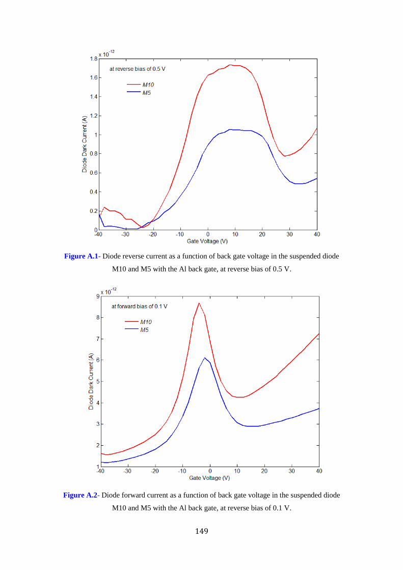
149
Figure A.1- Diode reverse current as a function of back gate voltage in the suspended diode
M10 and M5 with the Al back gate, at reverse bias of 0.5 V.
Figure A.2- Diode forward current as a function of back gate voltage in the suspended diode
M10 and M5 with the Al back gate, at reverse bias of 0.1 V.

150
2) Theoretical analysis
Under reverse-biased condition:
(a) Effective generation lifetime τg eff in silicon can be evaluated by using the
following simple expression:
(A.1)
where q is the elementary electric charge, tSi is the silicon film thickness, W and L are
the effective device width and length, respectively. IR max is the maximum
experimental reverse current measured under the reverse condition (e.g. at reverse
bias of 0.5 V in Figure A.1), which is the sum of all generation components in the
device with their maximum contributions. ni is the intrinsic carriers density.
(b) The carrier lifetime in the silicon film τgv can evaluated as below:
(A.2)
where the Isat is the saturation volume generation current (measured as a difference
between the inversion and accumulation plateau levels). And the tgen is the effective
generation layer width, defined as the depletion region where the electrons and holes
densities less than ni, which can be written as below:
(A.3)
(A.4)
where φF is the Fermi potential, φF= (kT/q)log(NA/ni), NA is the density of acceptor
impurities in the I-region. Equation (A.4) is a better approximation for tgen at high
temperature. kT/q is the thermal voltage, VR is the reverse bias of the PN junction.

151
(c) The rise edge Irise of the experimental current-voltage (i.e. reverse current versus
back gate voltage, IR-Vg) curve in Figure A.1 actually represents the surface
generation current at the font or back interface. The back-gate bias used in this
experiment is mainly altering the space-charge condition of the back interface, thus
the back surface generation velocity sg b can be extracted by using the following
expression:
(A.5)
Under forward-biased condition:
Under forward condition, the measured current peak represents the sum of the
maximum of all current components. The effective recombination lifetime from the
measured current peak Ipeak as:
(A.6)
(A.7)
where sf and sb are the surface recombination velocity at the front and back interface
respectively. VF is the reverse bias of the PN junction. The recombination lifetime in
the silicon film τrv in can be readily obtained as below:.
(A.8)
(A.9)
where tgen is the effective generation layer width estimated at forward bias. Ipeak is the
from the plateau current where surface recombination at both interfaces is effectively
suppressed in the plateau range. Combing equations (A.7), (A.8) and (A.9), the back
surface recombination velocity can be evaluated.

152
3) Numerical extraction
The parameters are extracted at room temperature of 25 °C, with doping concentration
of 5 × 10¹⁵
cm-3
and the diode width 60 µm. Table A.I lists the back surface
generation velocity and effective carriers’ lifetime under reverse bias, Table A.II lists
the back surface recombination velocity and effective carriers’ lifetime under forward
bias.
TABLE A.I
SURFACE GENERATION VELOCITY AND EFFECTIVE CARRIERS’ LIFETIME, AT REVERSE BIAS OF
0.5 V
Devices Back surface generation
velocity s (cm/s) Effective carriers’ lifetime eff (µs)
M5 177.4 0.12
M10 145.6 0.15
TABLE A.II
SURFACE RECOMBINATION VELOCITY AND EFFECTIVE CARRIERS’ VELOCITY, AT FORWARD
BIAS OF 0.1 V
Devices Back surface recombination
velocity s (cm/s) Effective carriers’ lifetime eff (µs)
M5 146.3 0.03
M10 103.9 0.04

153
Annex 2: A typical distribution of
interface trap density (Dit)
The Figure 10.10 in [48] is a typical distribution of interface trap density (Dit), as
reproduced in Figure A.3, where the interface states are distributed nonuniformly
throughout the forbidden gap. It consists of two high peaks near the conduction band
and valence band edges and a minimum near the middle of the band gap. The
acceptor- and donor-like traps are symmetrically distributed in the upper and lower
parts of Si band gap with two density peaks (~ 1×10¹²
cm-2
eV-1
) at 0.12 eV of Ec − Et
(for the acceptor-like traps DitA) and Et − Ev (for the donor-like traps DitD), where Et is
the trap energy position in the band gap, Ec is the conduction band energy of Si, and
Ev is the valence band energy of Si.
Figure A.3- A typical distribution of interface traps density Dit in the band gap of silicon.