Embed Size (px)
Citation preview
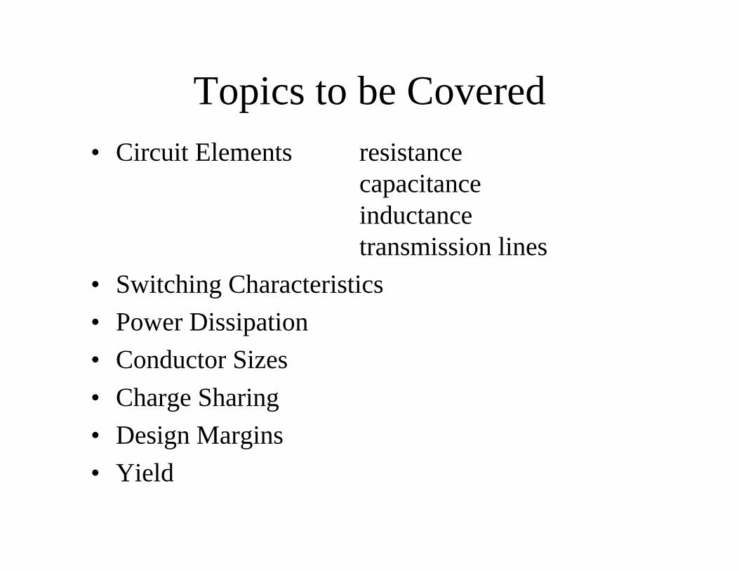
Topics to be Covered• Circuit Elements resistance
capacitanceinductancetransmission lines
• Switching Characteristics
• Power Dissipation
• Conductor Sizes
• Charge Sharing
• Design Margins
• Yield
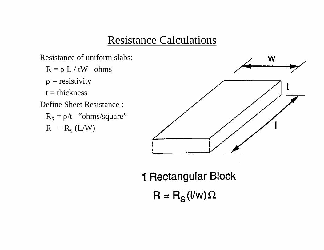
Resistance Calculations
Resistance of uniform slabs:
R = ρ L / tW ohms
ρ = resistivity
t = thickness
Define Sheet Resistance :
RS = ρ/t “ohms/square”
R = RS (L/W)
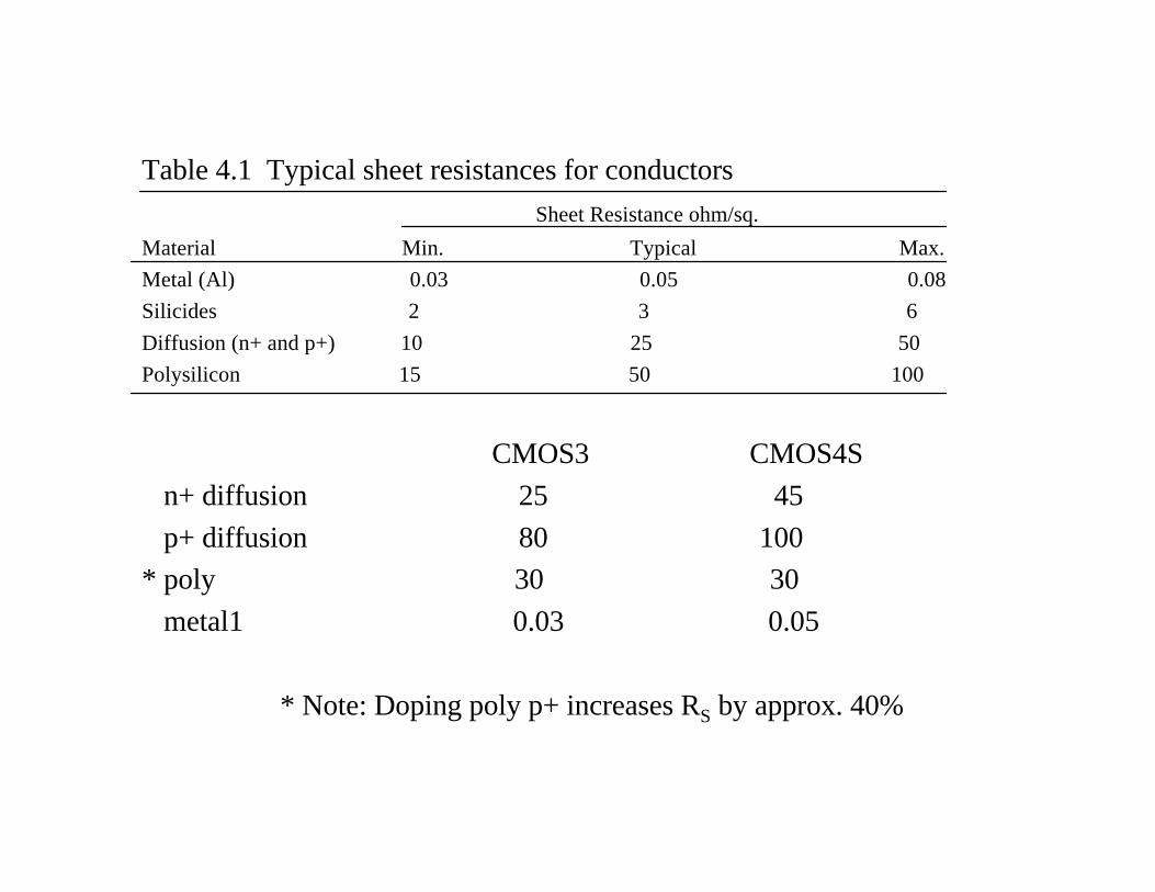
Table 4.1 Typical sheet resistances for conductors
Sheet Resistance ohm/sq.
Material Min. Typical Max.
Metal (Al) 0.03 0.05 0.08
Silicides 2 3 6
Diffusion (n+ and p+) 10 25 50
Polysilicon 15 50 100
CMOS3 CMOS4S
n+ diffusion 25 45
p+ diffusion 80 100
* poly 30 30
metal1 0.03 0.05
* Note: Doping poly p+ increases RS by approx. 40%
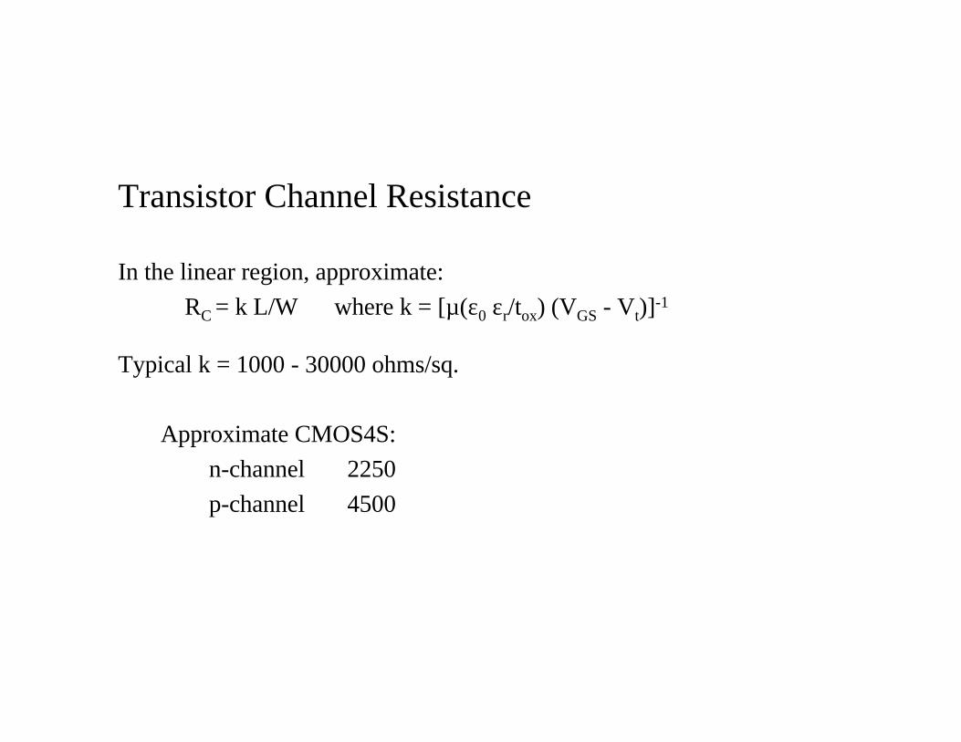
Transistor Channel Resistance
In the linear region, approximate:
RC = k L/W where k = [µ(ε0 εr/tox) (VGS - Vt)]-1
Typical k = 1000 - 30000 ohms/sq.
Approximate CMOS4S:
n-channel 2250
p-channel 4500
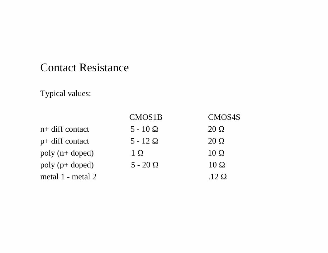
Contact Resistance
Typical values:
CMOS1B CMOS4S
n+ diff contact 5 - 10 Ω 20 Ωp+ diff contact 5 - 12 Ω 20 Ωpoly (n+ doped) 1 Ω 10 Ωpoly (p+ doped) 5 - 20 Ω 10 Ωmetal 1 - metal 2 .12 Ω
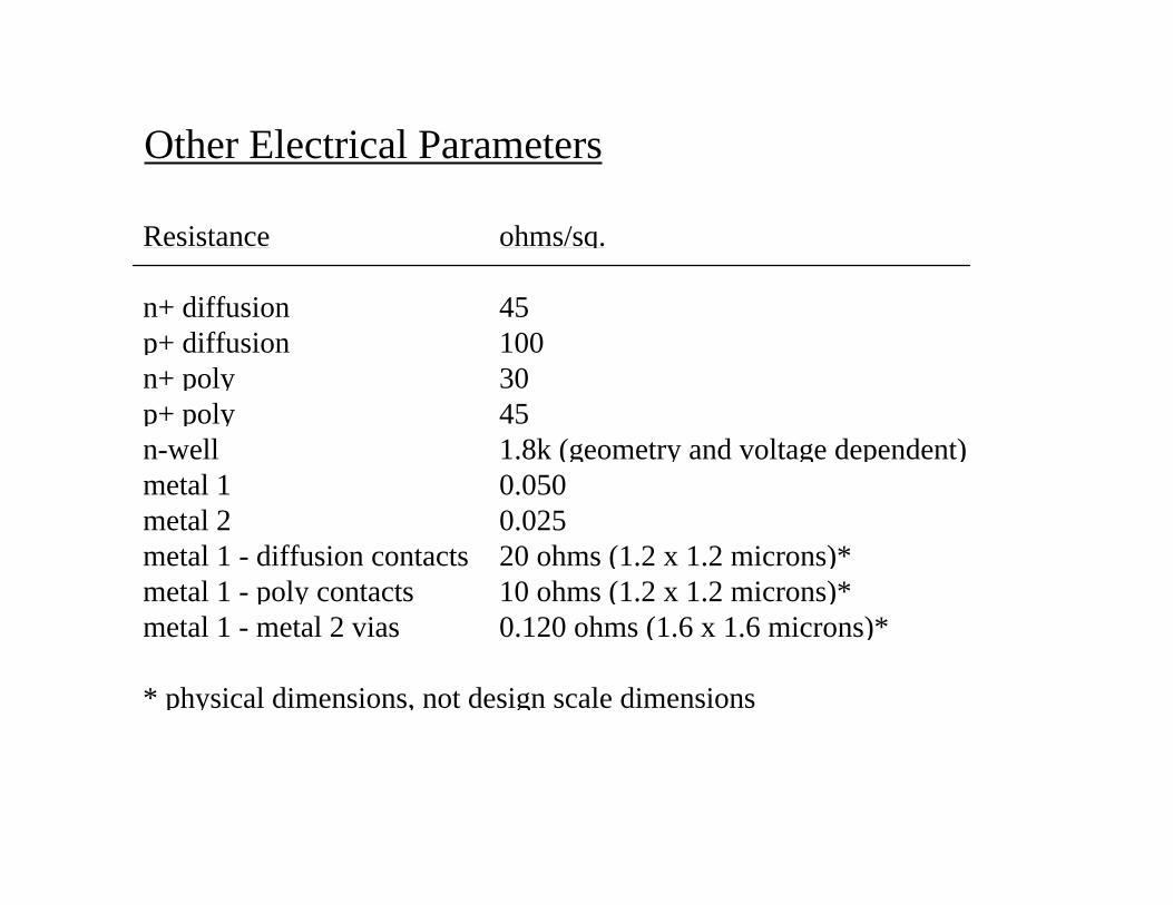
Other Electrical Parameters
Resistance ohms/sq.
n+ diffusion 45p+ diffusion 100n+ poly 30p+ poly 45n-well 1.8k (geometry and voltage dependent)metal 1 0.050metal 2 0.025metal 1 - diffusion contacts 20 ohms (1.2 x 1.2 microns)*metal 1 - poly contacts 10 ohms (1.2 x 1.2 microns)*metal 1 - metal 2 vias 0.120 ohms (1.6 x 1.6 microns)*
* physical dimensions, not design scale dimensions
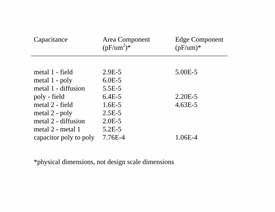
Capacitance Area Component(pF/um2)*
Edge Component(pF/um)*
metal 1 - field 2.9E-5 5.00E-5metal 1 - poly 6.0E-5metal 1 - diffusion 5.5E-5poly - field 6.4E-5 2.20E-5metal 2 - field 1.6E-5 4.63E-5metal 2 - poly 2.5E-5metal 2 - diffusion 2.0E-5metal 2 - metal 1 5.2E-5capacitor poly to poly 7.76E-4 1.06E-4
*physical dimensions, not design scale dimensions
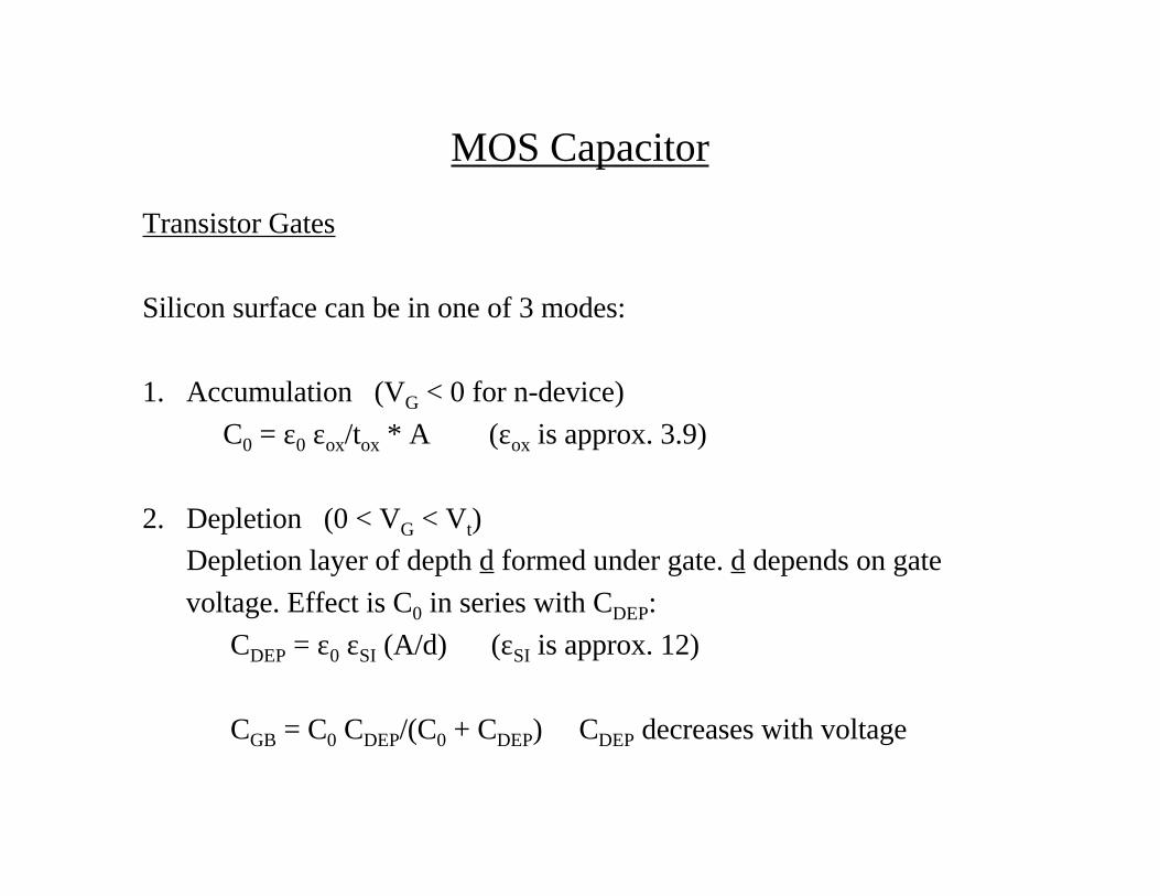
MOS Capacitor
Transistor Gates
Silicon surface can be in one of 3 modes:
1. Accumulation (VG < 0 for n-device)
C0 = ε0 εox/tox * A (εox is approx. 3.9)
2. Depletion (0 < VG < Vt)
Depletion layer of depth d formed under gate. d depends on gate
voltage. Effect is C0 in series with CDEP:
CDEP = ε0 εSI (A/d) (εSI is approx. 12)
CGB = C0 CDEP/(C0 + CDEP) CDEP decreases with voltage
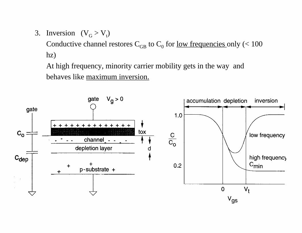
3. Inversion (VG > Vt)
Conductive channel restores CGB to C0 for low frequencies only (< 100
hz)
At high frequency, minority carrier mobility gets in the way and
behaves like maximum inversion.
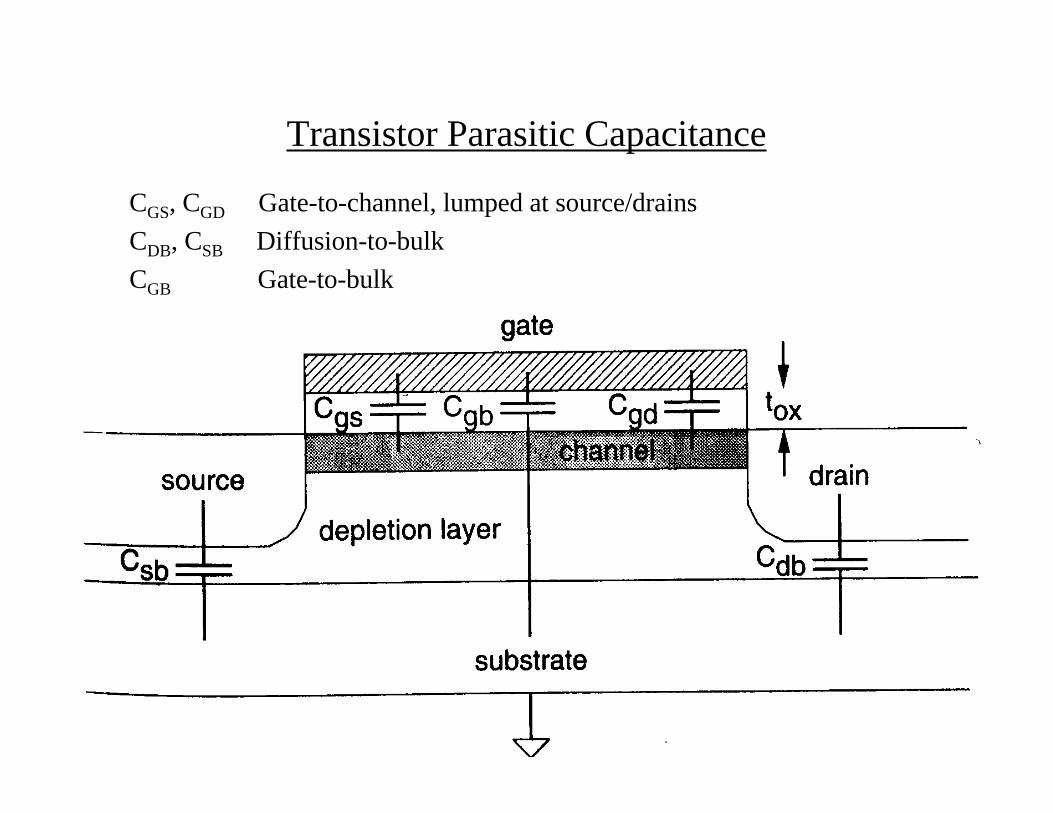
Transistor Parasitic Capacitance
CGS, CGD Gate-to-channel, lumped at source/drains
CDB, CSB Diffusion-to-bulk
CGB Gate-to-bulk
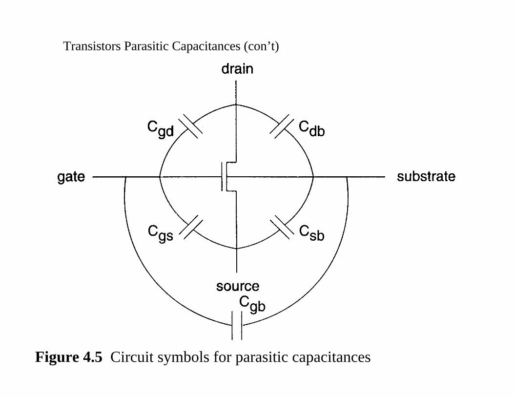
Transistors Parasitic Capacitances (con’t)
Figure 4.5 Circuit symbols for parasitic capacitances
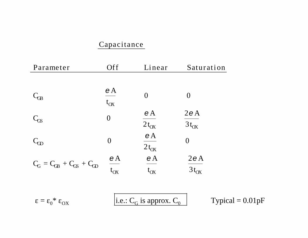
C a p a c i t a n c e
P a r a m e t e r O f f L i n e a r S a t u r a t i o n
C A
t 0 0
C 0 A
2 t
2 A
3 t
C 0 A
2 t 0
C = C + C + C A
t
A
t
2 A
3 t
GBOX
GSOX OX
GDOX
G GB GS GDOX OX OX
ε
ε ε
ε
ε ε ε
ε = ε0* εOX i.e.: CG is approx. C0 Typical = 0.01pF
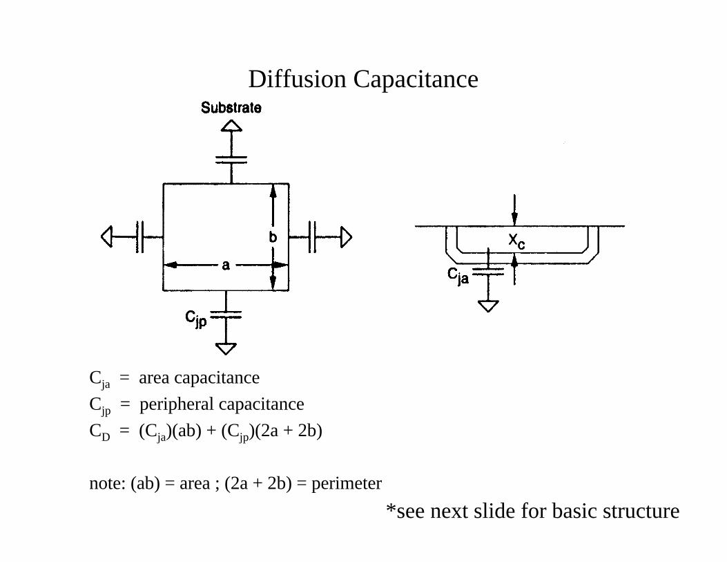
Diffusion Capacitance
Cja = area capacitance
Cjp = peripheral capacitance
CD = (Cja)(ab) + (Cjp)(2a + 2b)
note: (ab) = area ; (2a + 2b) = perimeter
*see next slide for basic structure
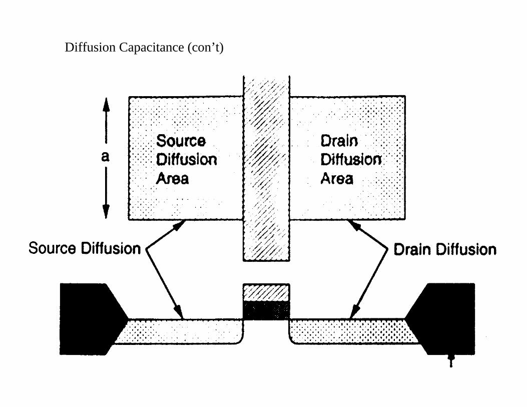
Diffusion Capacitance (con’t)
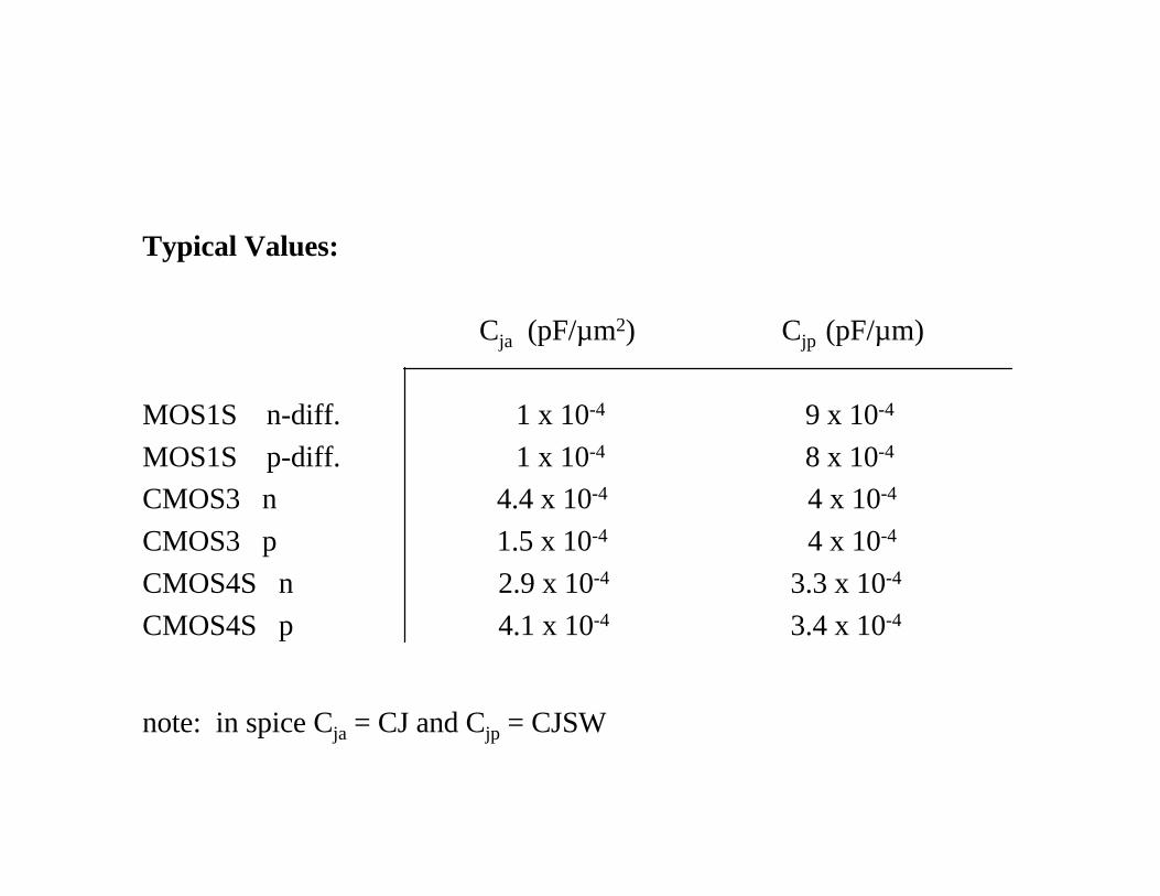
Typical Values:
Cja (pF/µm2) Cjp (pF/µm)
MOS1S n-diff. 1 x 10⁻⁴ 9 x 10⁻⁴
MOS1S p-diff. 1 x 10⁻⁴ 8 x 10⁻⁴
CMOS3 n 4.4 x 10⁻⁴ 4 x 10⁻⁴
CMOS3 p 1.5 x 10⁻⁴ 4 x 10⁻⁴
CMOS4S n 2.9 x 10⁻⁴ 3.3 x 10⁻⁴
CMOS4S p 4.1 x 10⁻⁴ 3.4 x 10⁻⁴
note: in spice Cja = CJ and Cjp = CJSW
Inductance
• Normally not a problem for on-chip wires.
• Can be a problem for bonding wires.
• On-chip L = 20 pH/mm
• Bonding wire and package inductance =3-15 nH.
• V = LdI/dt = (5nH)(2.5mA)/(1ns) = 12.5mV
• Only a problem for high performance chips.
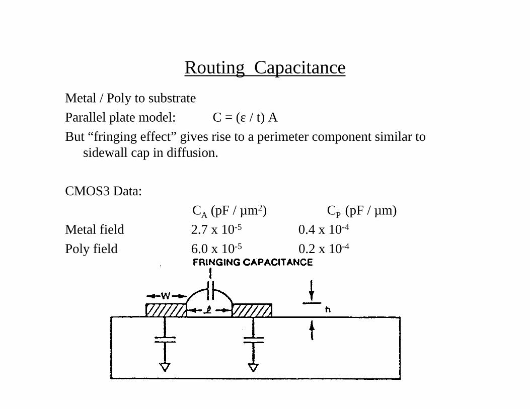
Routing Capacitance
Metal / Poly to substrate
Parallel plate model: C = (ε / t) ABut “fringing effect” gives rise to a perimeter component similar to
sidewall cap in diffusion.
CMOS3 Data:
CA (pF / µm2) CP (pF / µm)
Metal field 2.7 x 10⁻⁵ 0.4 x 10⁻⁴
Poly field 6.0 x 10⁻⁵ 0.2 x 10⁻⁴
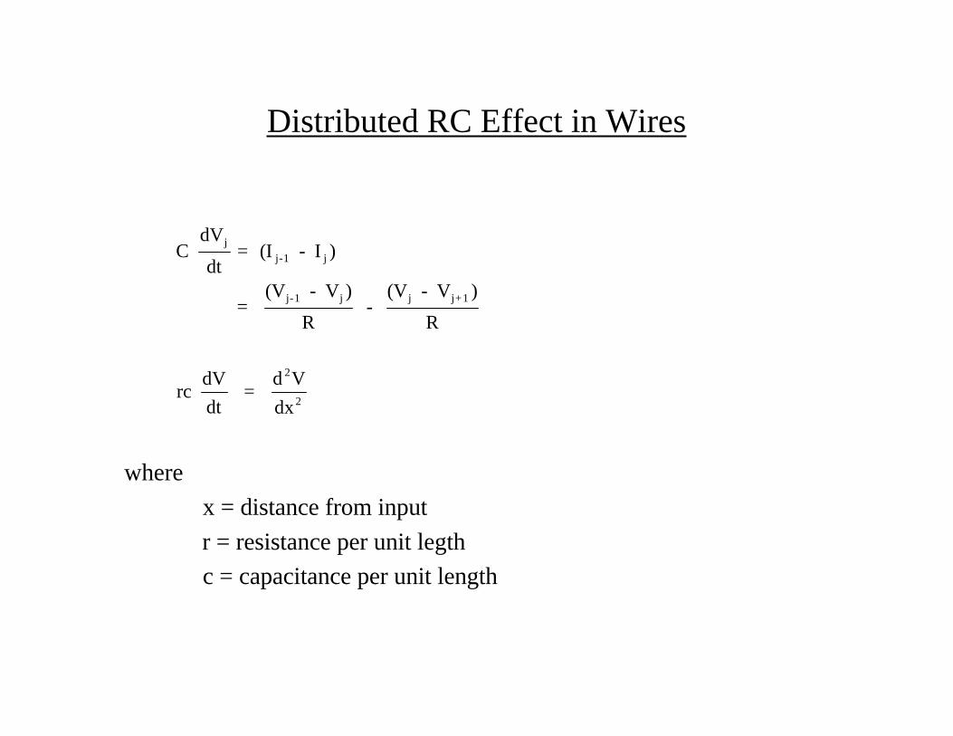
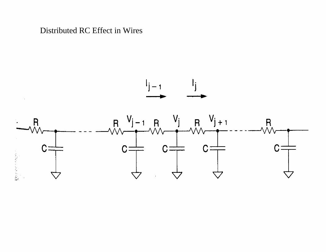
Distributed RC Effect in Wires
where
x = distance from input
r = resistance per unit legth
c = capacitance per unit length
C dV
dt (I - I )
= (V - V )
R -
(V - V )
R
rc dV
dt =
d V
dx
j
j-1 j
j-1 j j j+1
2
2
=
Distributed RC Effect in Wires
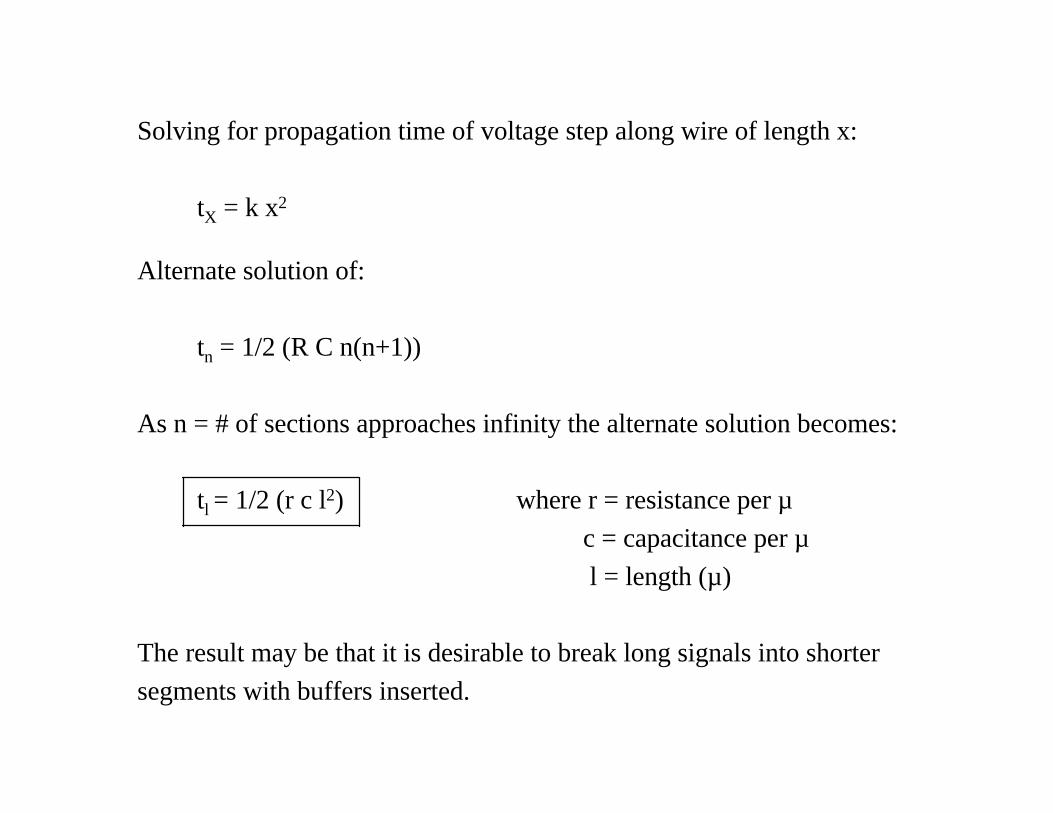
Solving for propagation time of voltage step along wire of length x:
tX = k x2
Alternate solution of:
tn = 1/2 (R C n(n+1))
As n = # of sections approaches infinity the alternate solution becomes:
tl = 1/2 (r c l2) where r = resistance per µ c = capacitance per µ l = length (µ)
The result may be that it is desirable to break long signals into shorter
segments with buffers inserted.
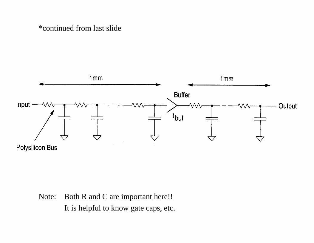
*continued from last slide
Note: Both R and C are important here!!
It is helpful to know gate caps, etc.
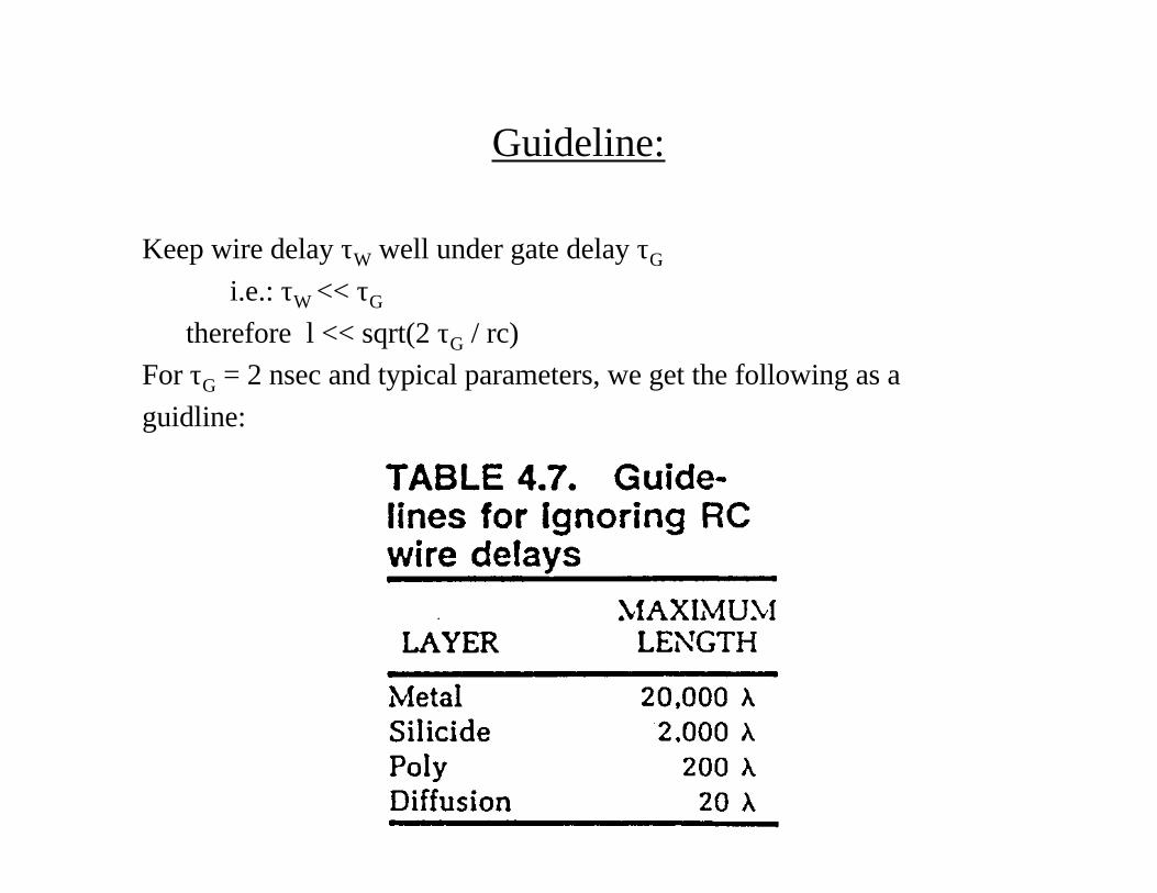
Keep wire delay τW well under gate delay τG
i.e.: τW << τG
therefore l << sqrt(2 τG / rc)
For τG = 2 nsec and typical parameters, we get the following as a
guidline:
Guideline:
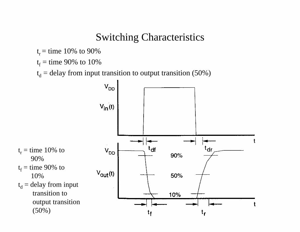
Switching Characteristicstr = time 10% to 90%
tf = time 90% to 10%
td = delay from input transition to output transition (50%)
tr = time 10% to 90%tf = time 90% to 10%td = delay from input transition to output transition (50%)
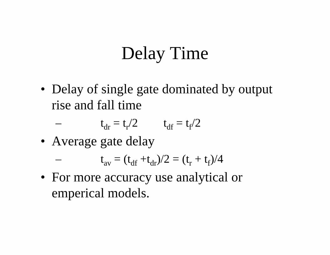
Delay Time
• Delay of single gate dominated by outputrise and fall time– tdr = tr/2 tdf = tf/2
• Average gate delay– tav = (tdf +tdr)/2 = (tr + tf)/4
• For more accuracy use analytical oremperical models.
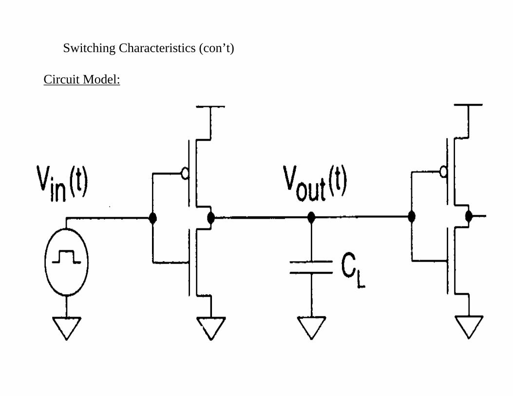
Switching Characteristics (con’t)
Circuit Model:
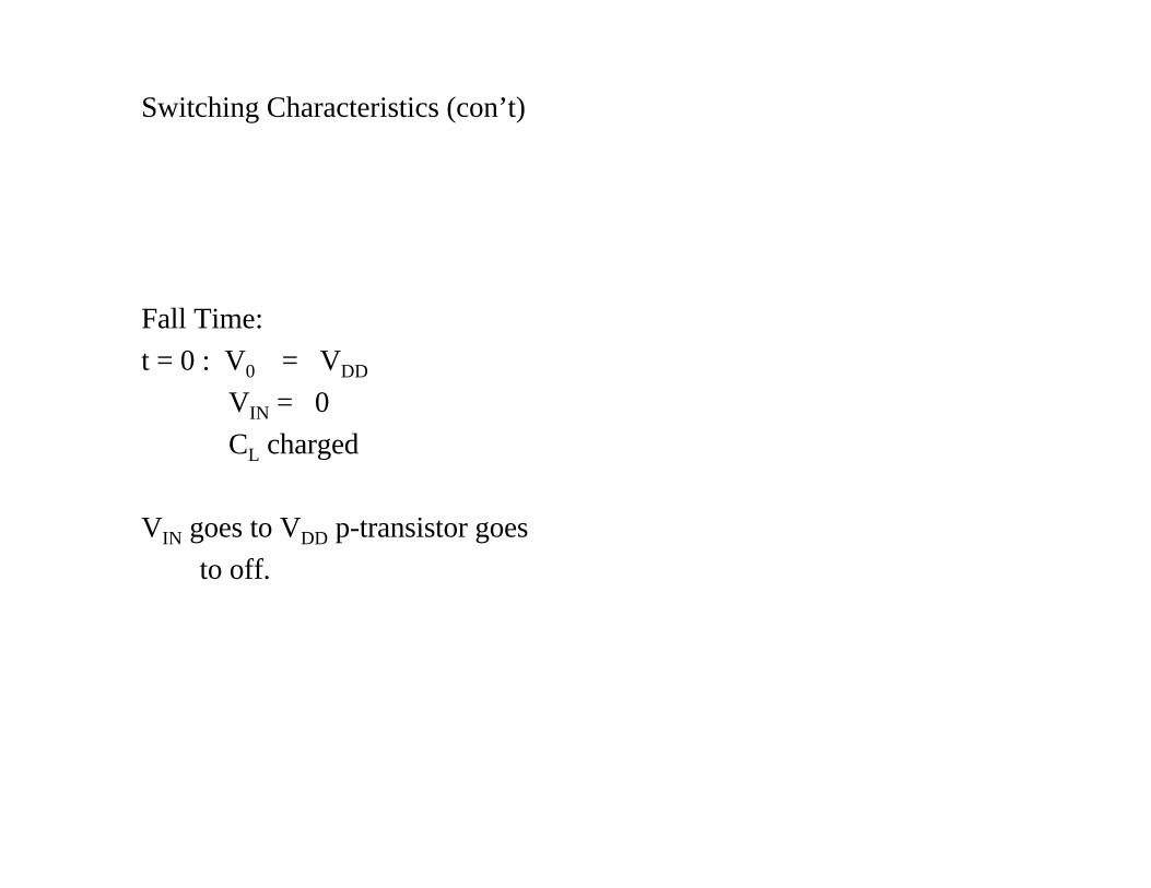
Switching Characteristics (con’t)
Fall Time:
t = 0 : V0 = VDD
VIN = 0
CL charged
VIN goes to VDD p-transistor goes
to off.
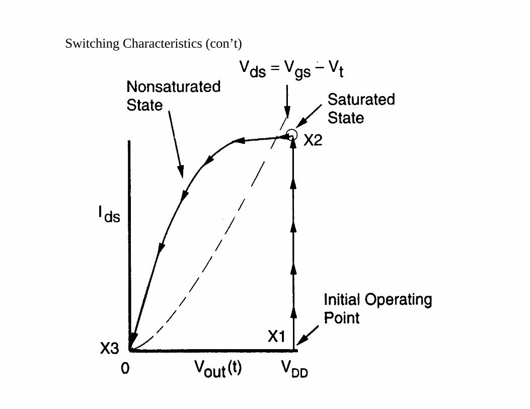
Switching Characteristics (con’t)
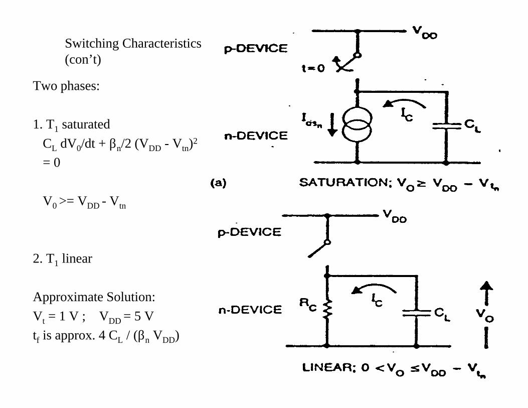
Switching Characteristics(con’t)
Two phases:
1. T1 saturated
CL dV0/dt + βn/2 (VDD - Vtn)2
= 0
V0 >= VDD - Vtn
2. T1 linear
Approximate Solution:
Vt = 1 V ; VDD = 5 V
tf is approx. 4 CL / (βn VDD)
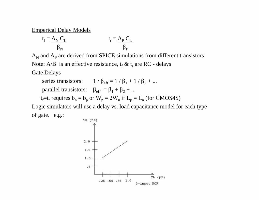
Emperical Delay Models
tf = AN CL tr = AP CL
βN βP
AN and AP are derived from SPICE simulations from different transistors
Note: A/B is an effective resistance, tf & tr are RC - delays
Gate Delays
series transistors: 1 / βeff = 1 / β1 + 1 / β2 + ...
parallel transistors: βeff = β1 + β2 + ...
tf=tr requires bn = bp or Wp = 2Wn if Lp = Ln (for CMOS4S)
Logic simulators will use a delay vs. load capacitance model for each type
of gate. e.g.:
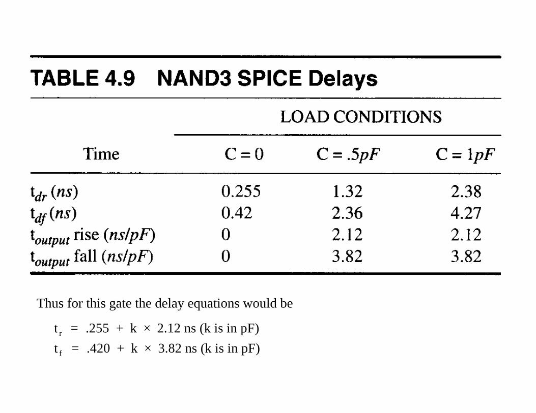
Thus for this gate the delay equations would be
t = .255 + k 2.12 ns (k is in pF)
t = .420 + k 3.82 ns (k is in pF)r
f
××
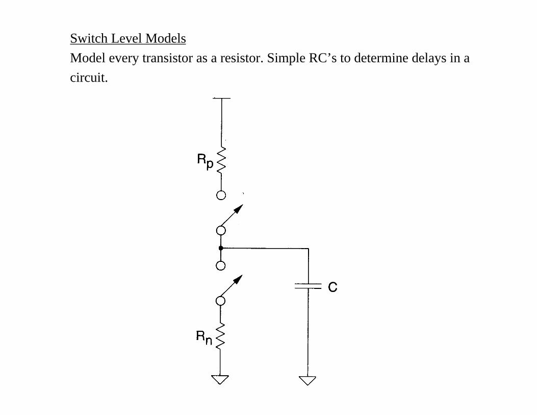
Switch Level Models
Model every transistor as a resistor. Simple RC’s to determine delays in a
circuit.
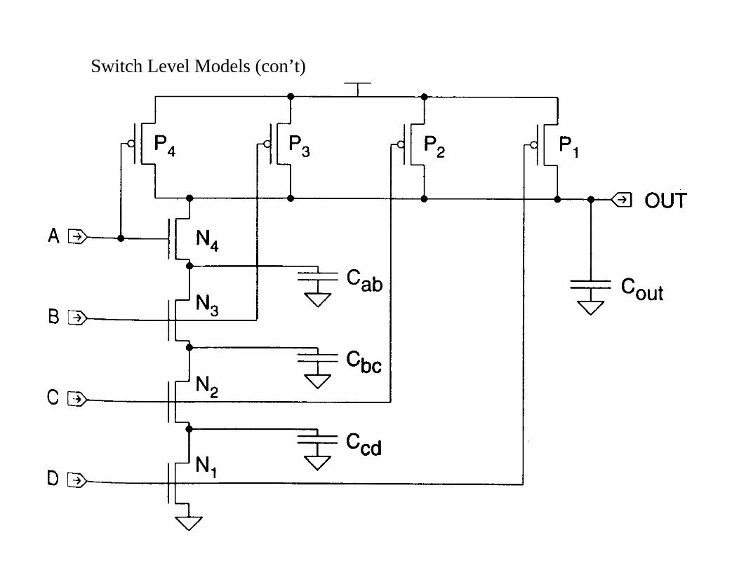
Switch Level Models (con’t)
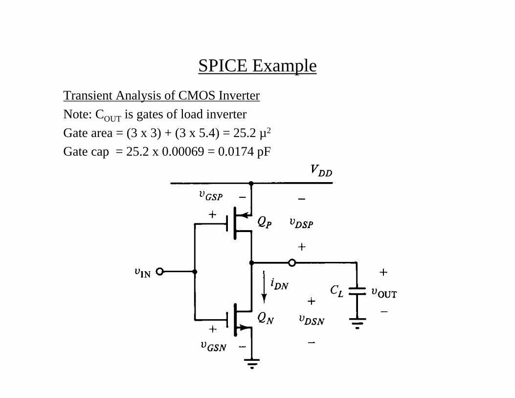
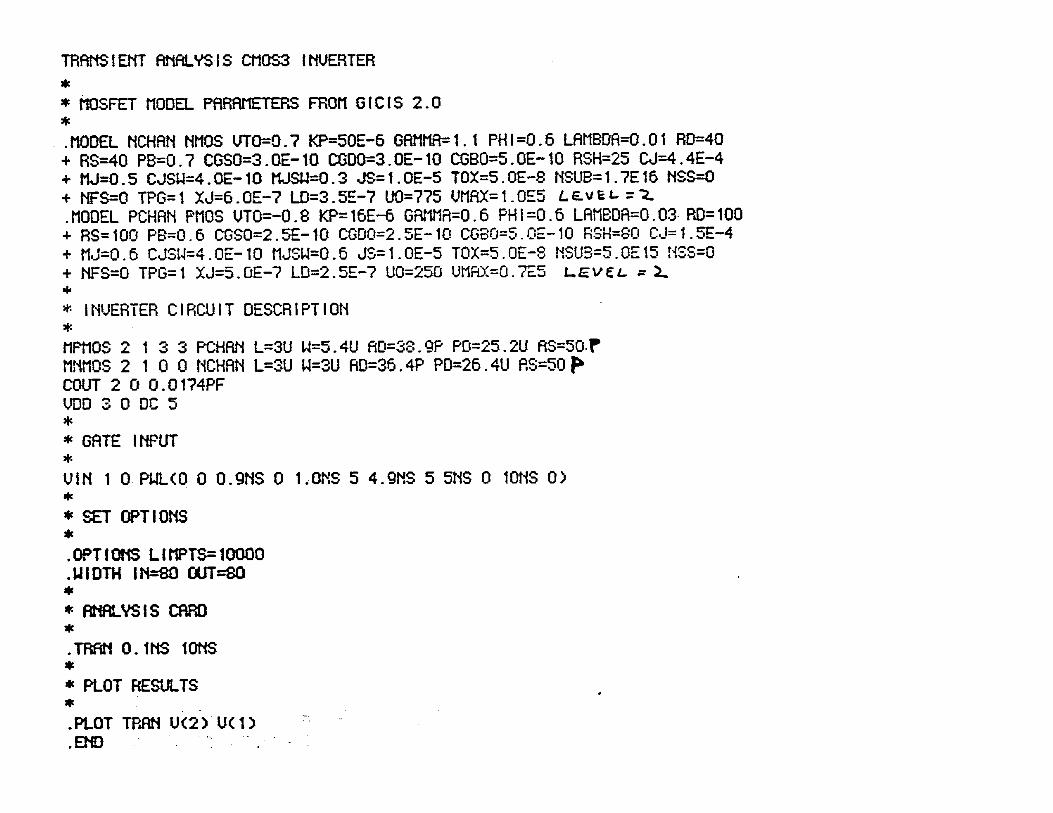
SPICE Example
Transient Analysis of CMOS Inverter
Note: COUT is gates of load inverter
Gate area = (3 x 3) + (3 x 5.4) = 25.2 µ2
Gate cap = 25.2 x 0.00069 = 0.0174 pF
Cascaded Stages
- It is better to drive a large load with a number of inverters (which
increase in size) than with a single small inverter
- Stage ratios vary from 2 - 10 with approx. 2.7 giving optimum speed
Power Dissipation
Static - Leakage currents
(0.1 - 0.5 nA) per device
PS is approx. 0.5 - 2.5 nW
Dynamic - Switching transient current
- Charge and discharge of load capacitance
PD = CLVDD2fP
For large circuits difficult to estimate what percentage of nodes are
switching, typically assume 50% if unknown
Conductor Sizes
- Always metal power lines
- Metal migration
: current density < 0.25 mA/µm
- Power supply noise
: power and ground bounce
- RC delay
- Large number of small contacts (vias) when changing layers
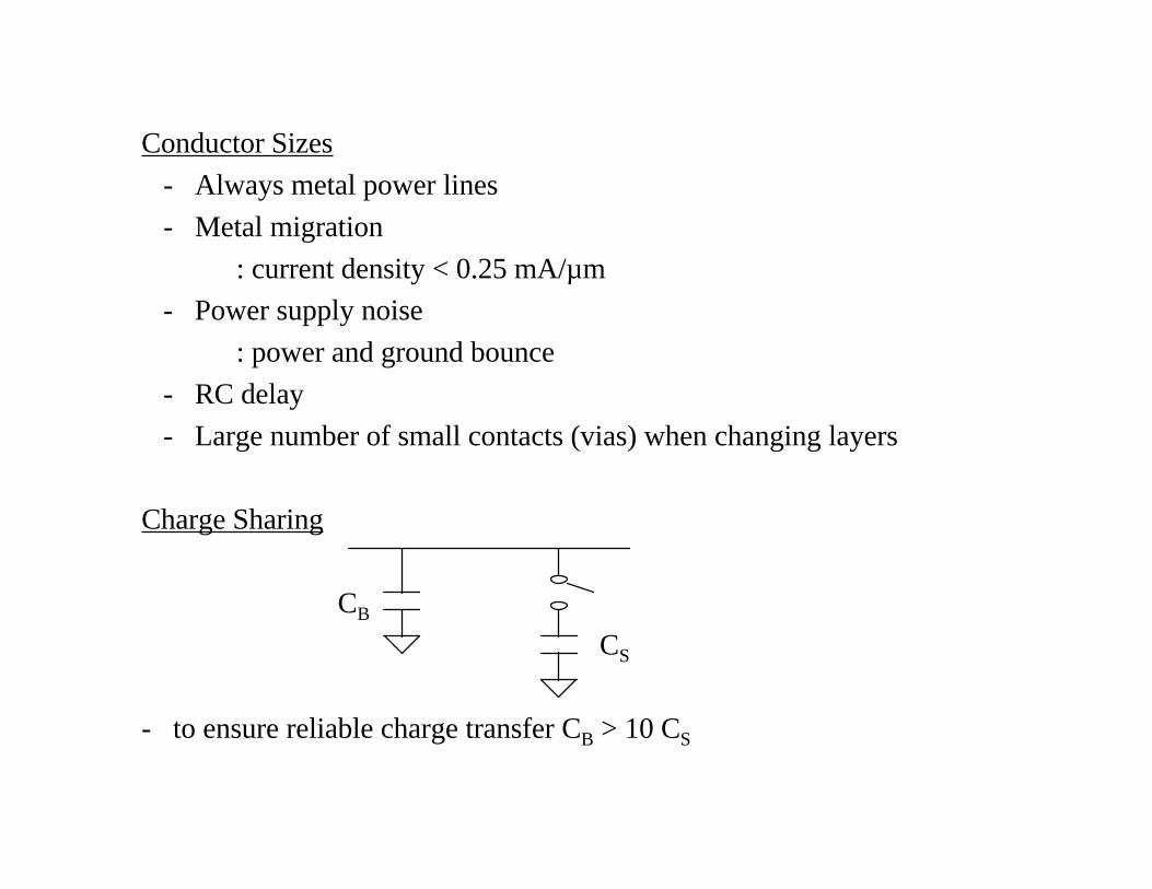
Charge Sharing
CB
CS
- to ensure reliable charge transfer CB > 10 CS
Design Margins
- Temperature:
commercial : 0 - 70oC
industrial : -40 - 85oC
military : -55 - 125oC
- Supply Voltage
+/- 10%
- Process Variations
2 - 3σ
∗see next slide for the diagram
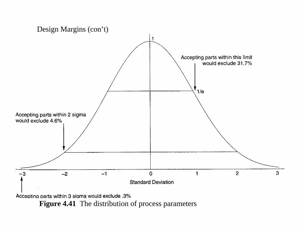
Design Margins (con’t)
Figure 4.41 The distribution of process parameters
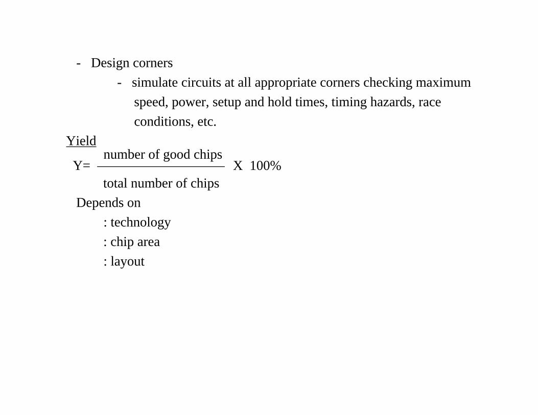
- Design corners
- simulate circuits at all appropriate corners checking maximum
speed, power, setup and hold times, timing hazards, race
conditions, etc.
Yield number of good chips Y= X 100% total number of chips
Depends on
: technology
: chip area
: layout
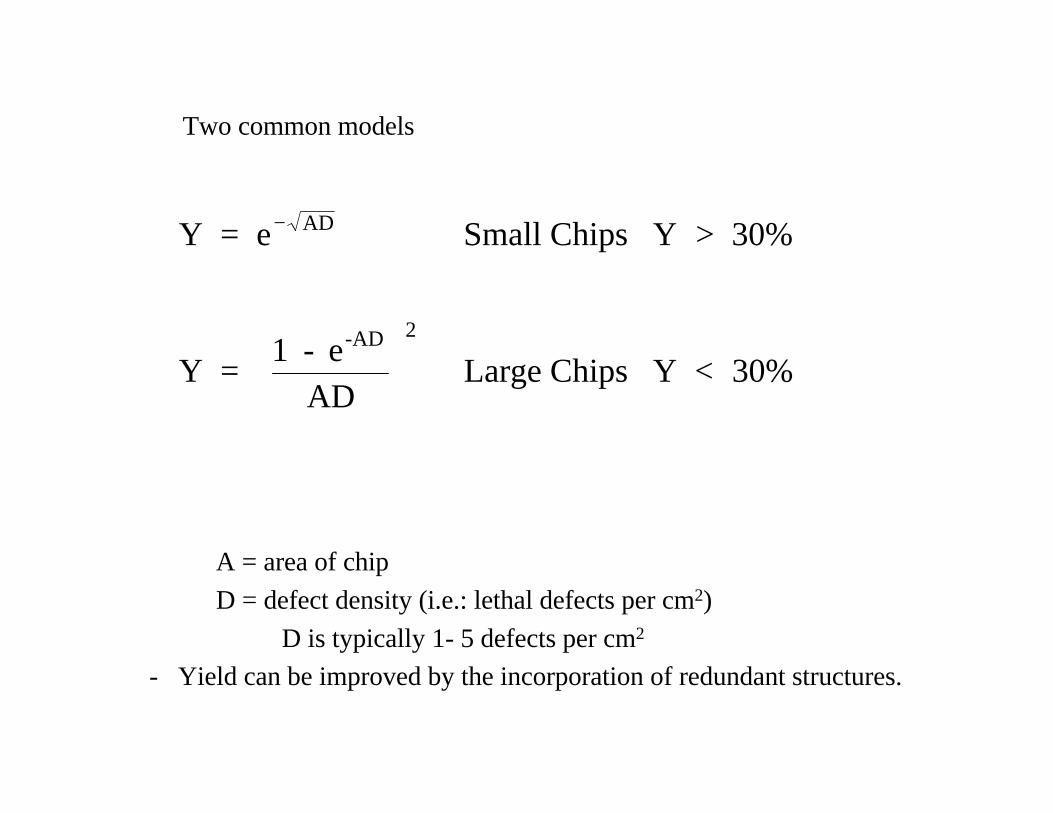
Two common models
Y = e Small Chips Y > 30%
Y = 1 - e
AD Large Chips Y < 30%
AD
-AD
−
2
A = area of chip
D = defect density (i.e.: lethal defects per cm2)
D is typically 1- 5 defects per cm2
- Yield can be improved by the incorporation of redundant structures.
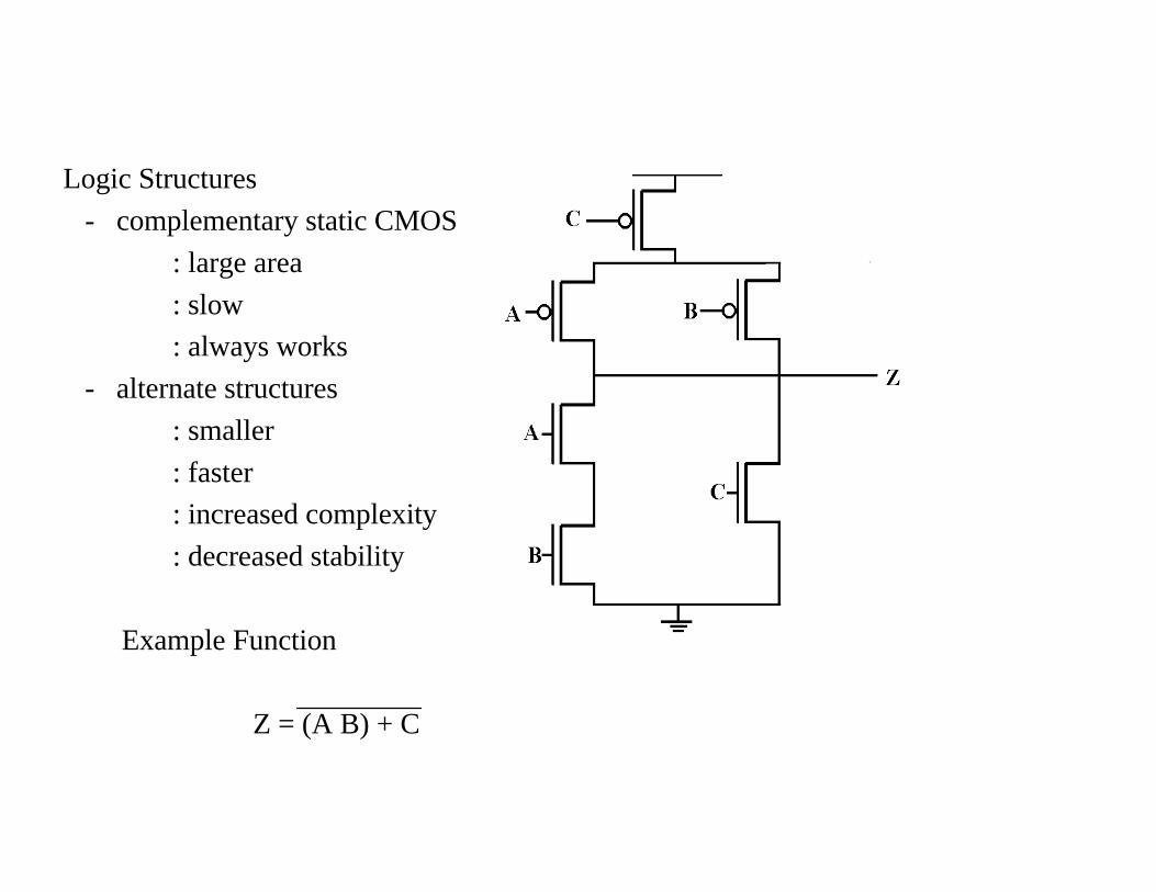
Logic Structures
- complementary static CMOS
: large area
: slow
: always works
- alternate structures
: smaller
: faster
: increased complexity
: decreased stability
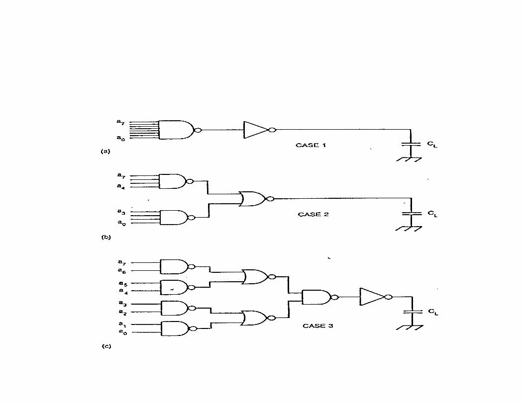
Example Function
Z = (A B) + C
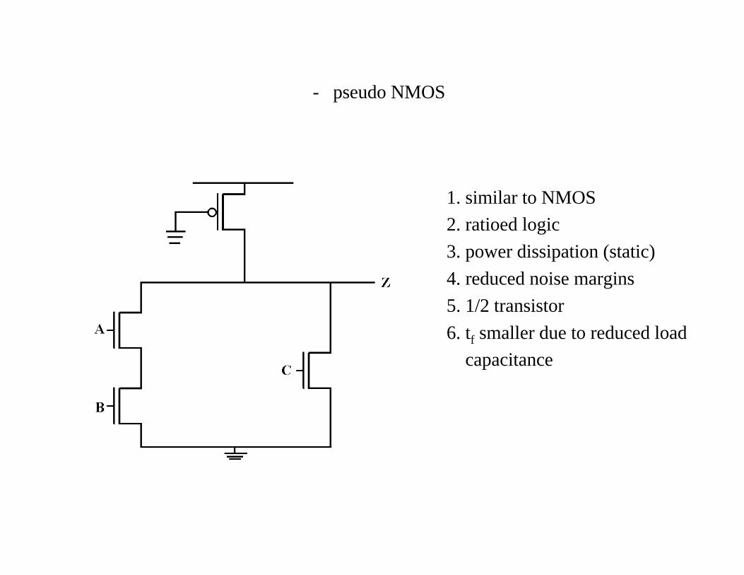
- pseudo NMOS
1. similar to NMOS
2. ratioed logic
3. power dissipation (static)
4. reduced noise margins
5. 1/2 transistor
6. tf smaller due to reduced load
capacitance
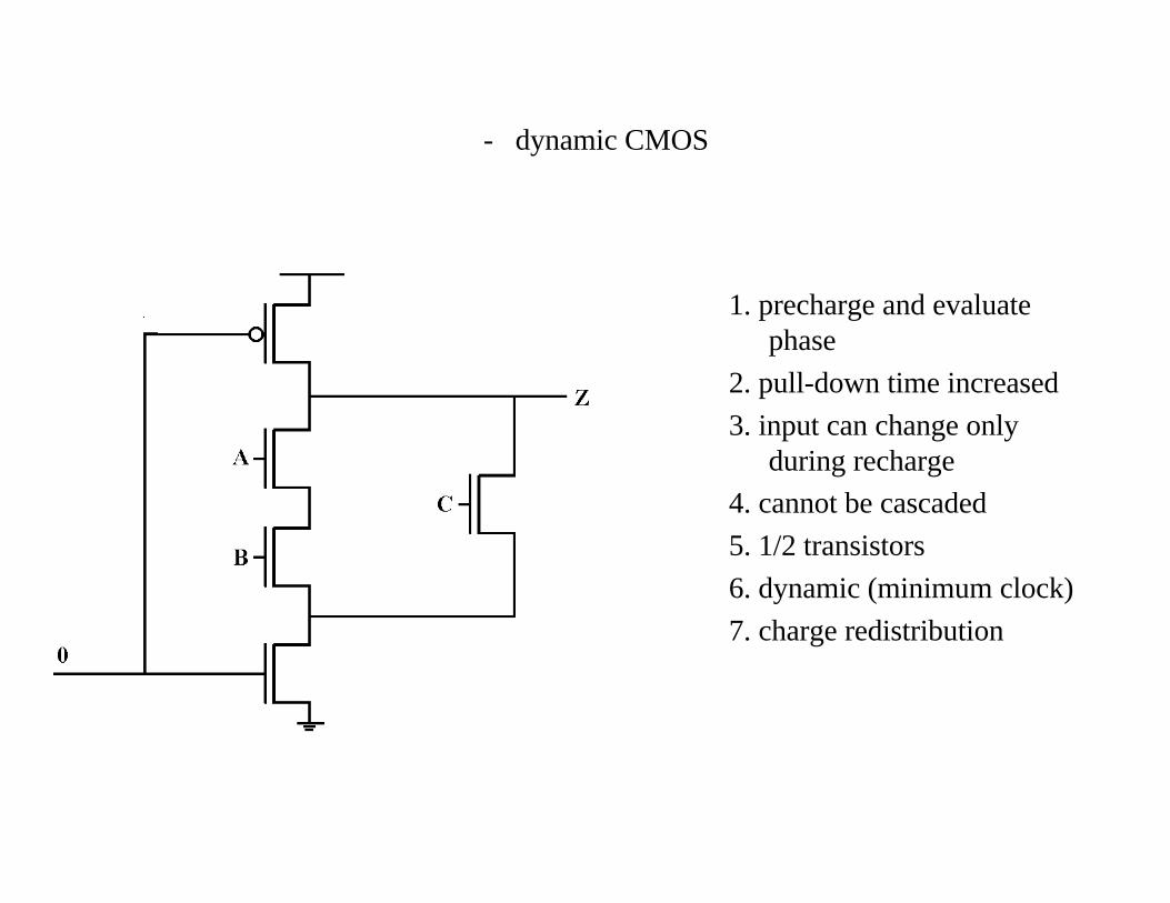
- dynamic CMOS
1. precharge and evaluatephase
2. pull-down time increased
3. input can change onlyduring recharge
4. cannot be cascaded
5. 1/2 transistors
6. dynamic (minimum clock)
7. charge redistribution
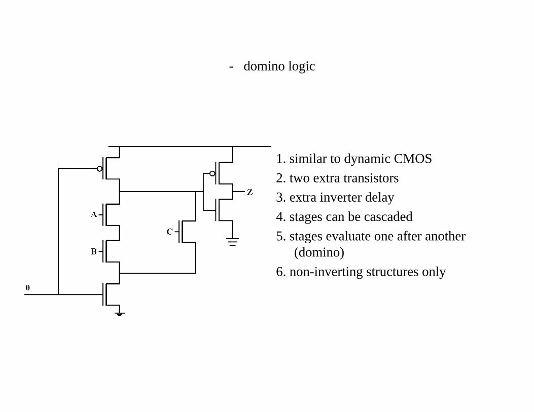
- domino logic
1. similar to dynamic CMOS
2. two extra transistors
3. extra inverter delay
4. stages can be cascaded
5. stages evaluate one after another(domino)
6. non-inverting structures only
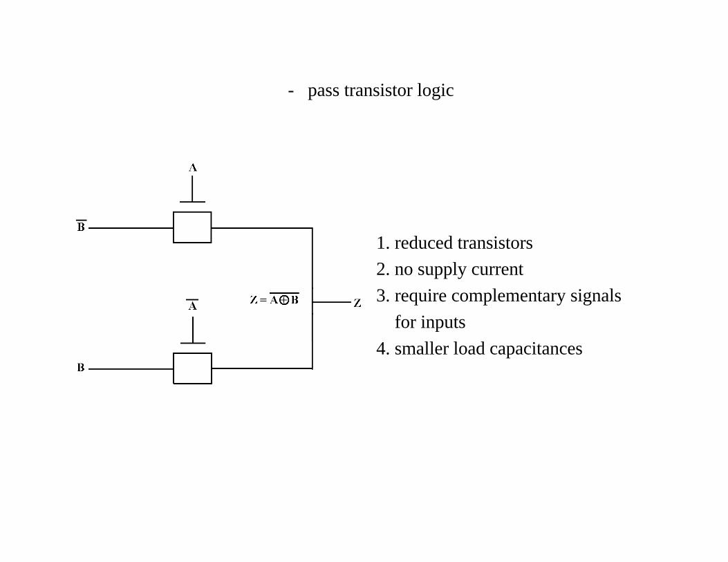
- pass transistor logic
1. reduced transistors
2. no supply current
3. require complementary signals
for inputs
4. smaller load capacitances
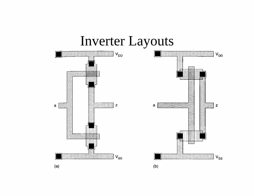
Inverter Layouts
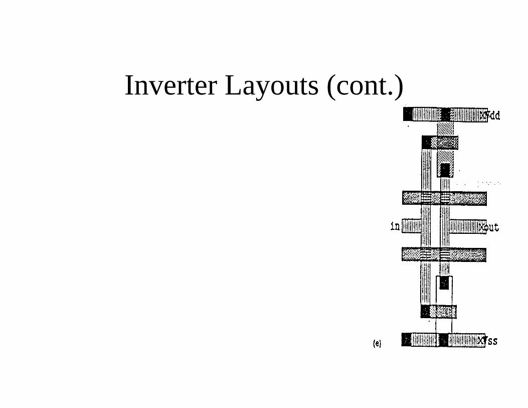
Inverter Layouts (cont.)
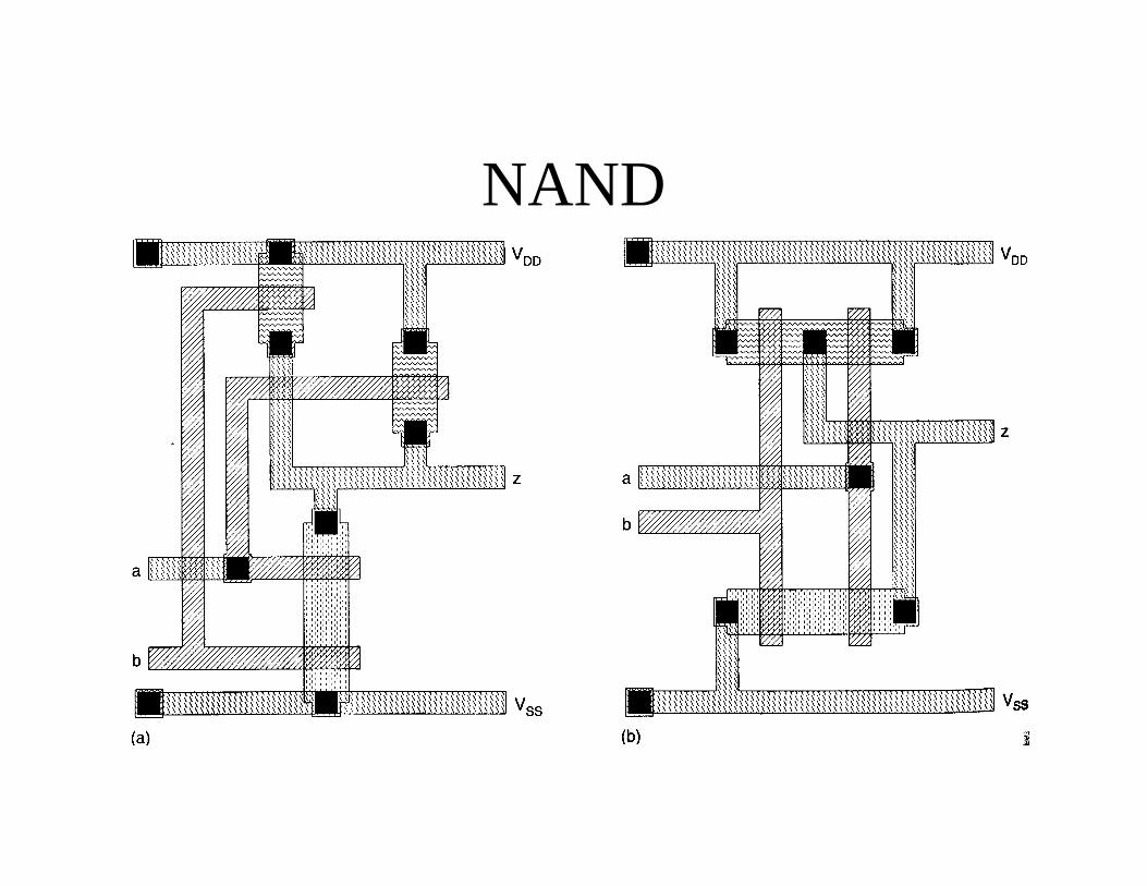
NAND
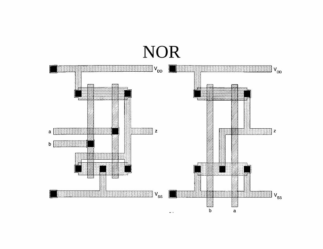
NOR
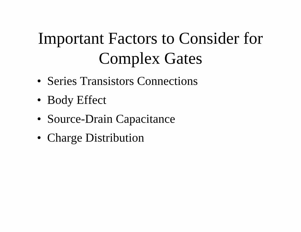
Important Factors to Consider forComplex Gates
• Series Transistors Connections
• Body Effect
• Source-Drain Capacitance
• Charge Distribution
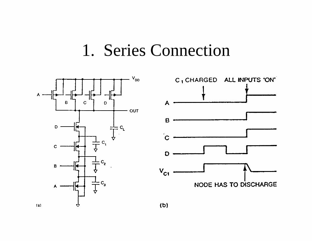
1. Series Connection
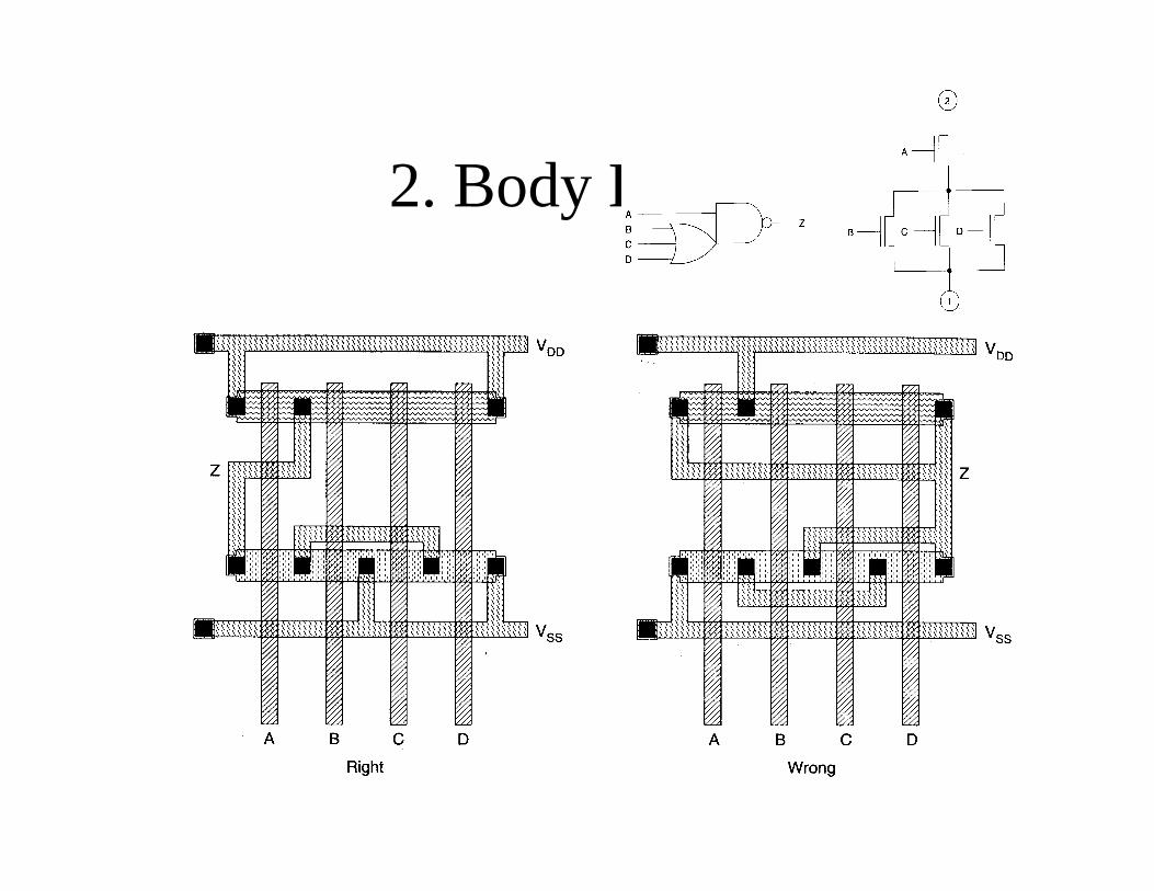
2. Body Effect
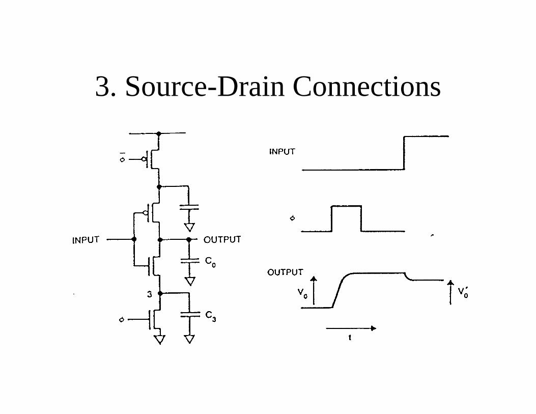
3. Source-Drain Connections
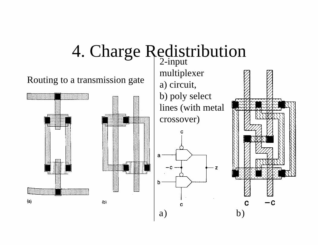
4. Charge Redistribution
Routing to a transmission gate
2-inputmultiplexera) circuit,b) poly selectlines (with metalcrossover)
a) b)
Charge Redistribution (con’t)
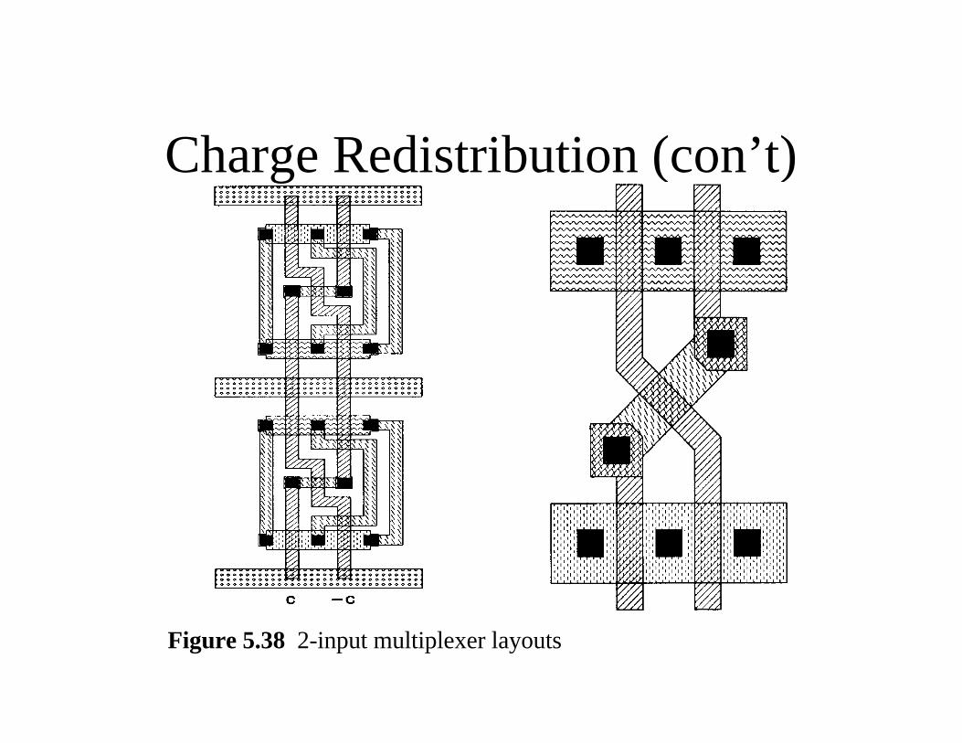
Figure 5.38 2-input multiplexer layouts
Summary
• complementary logic is the best option inmost CMOS circuits
• noise immunity
• low DC power dissipation
• generally fast
• creation is highly automated
• pseudo-NMOS finds use in large fan-inNOR gates
• e.g. ROMs, PLAs, carry look-ahead adders
Summary (cont.)
• higher static power dissipation
• clocked CMOS logic offers some relief forhot electron processes and conditions
• pass logic is fast if structures are limited toa few series transmission gates
• no CAD support for synthesis
Summary (cont.)
• domino logic useful for low-power highspeed applications
• charge redistribution
• requires lots of simulation/development time
• speed advantage diminishes in poorly designedclock schemes (i.e. precharge time)
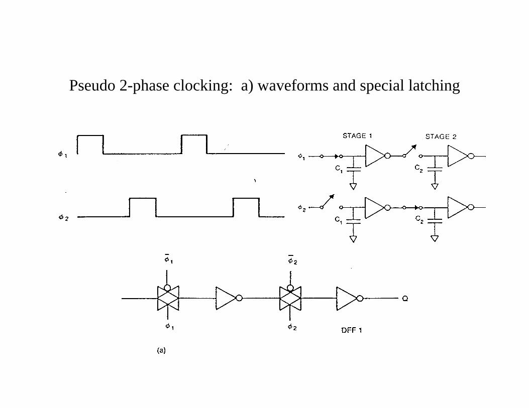
Pseudo 2-phase clocking: a) waveforms and special latching
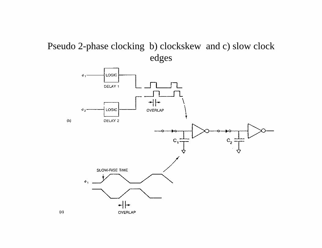
Pseudo 2-phase clocking b) clockskew and c) slow clockedges
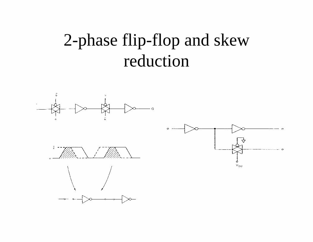
2-phase flip-flop and skewreduction
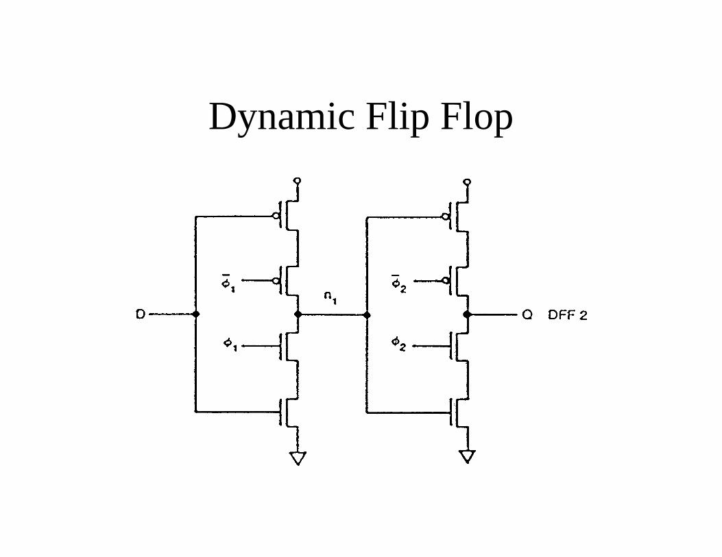
Dynamic Flip Flop
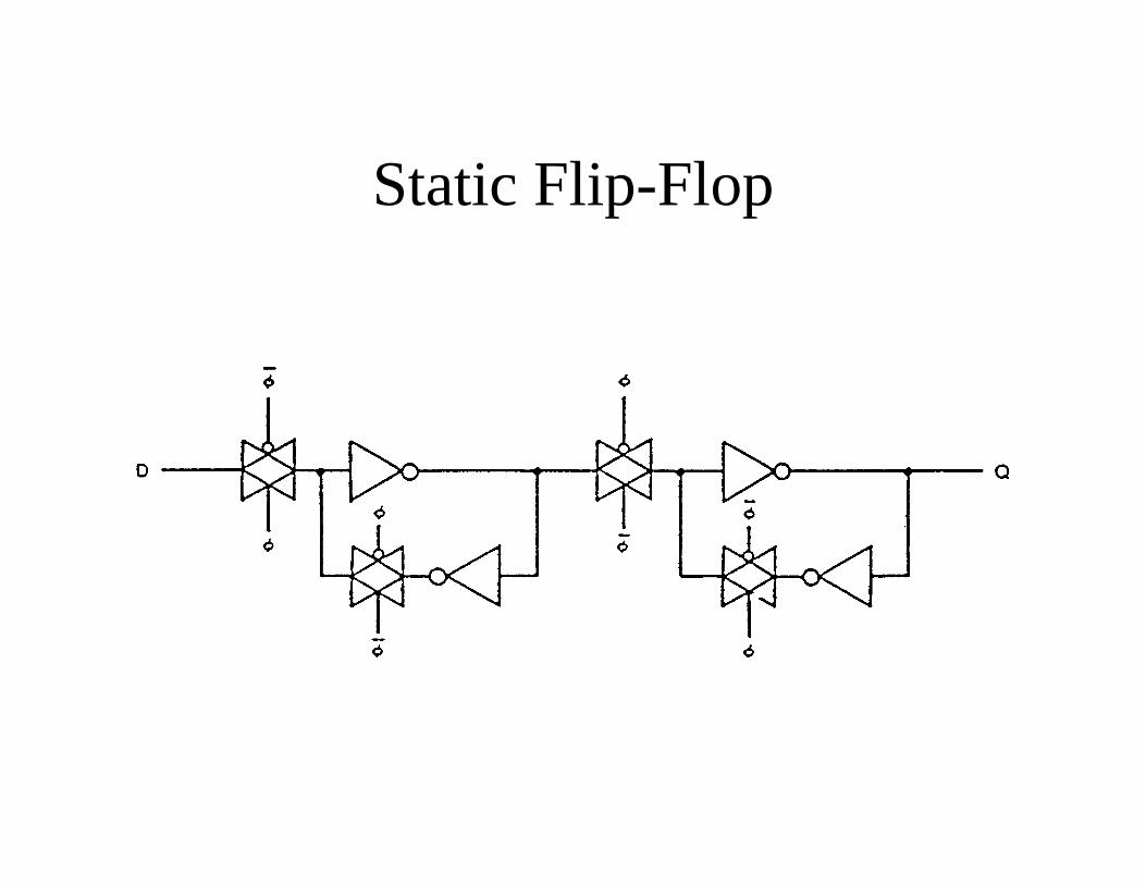
Static Flip-Flop
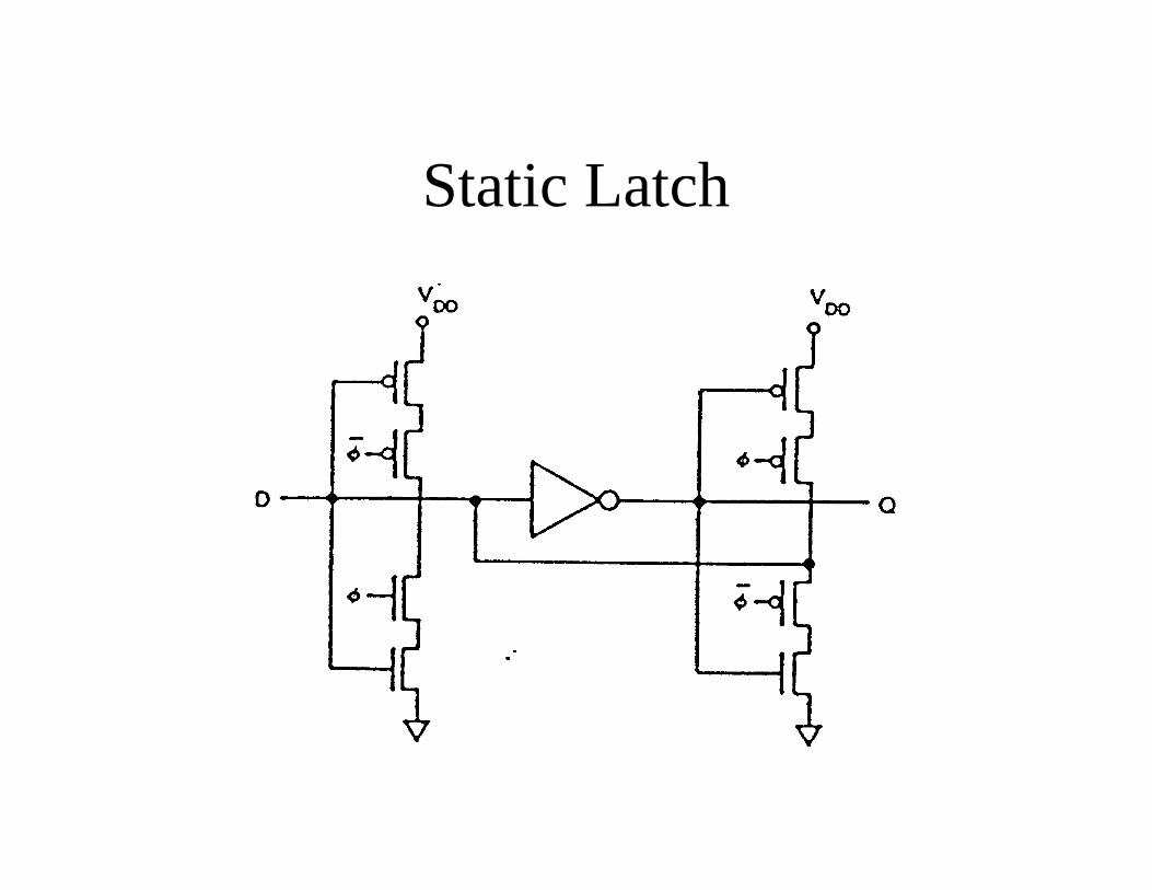
Static Latch
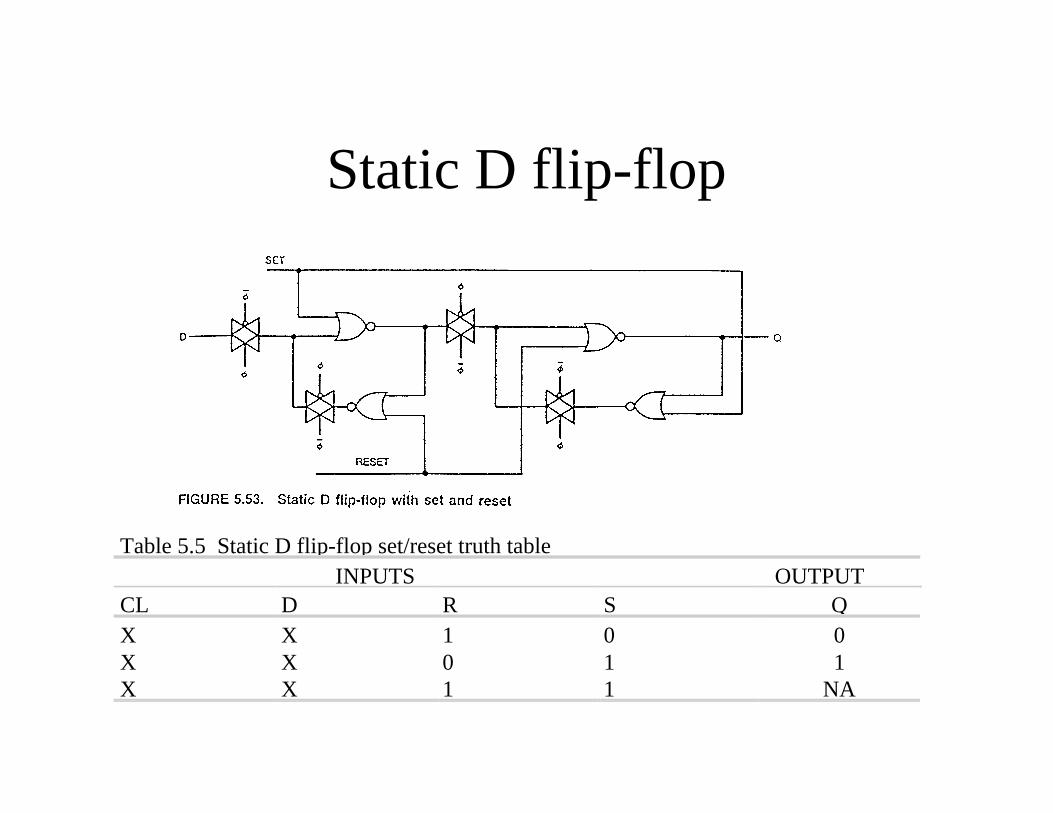
Table 5.5 Static D flip-flop set/reset truth table INPUTS OUTPUT
CL D R S QX X 1 0 0X X 0 1 1X X 1 1 NA
Static D flip-flop
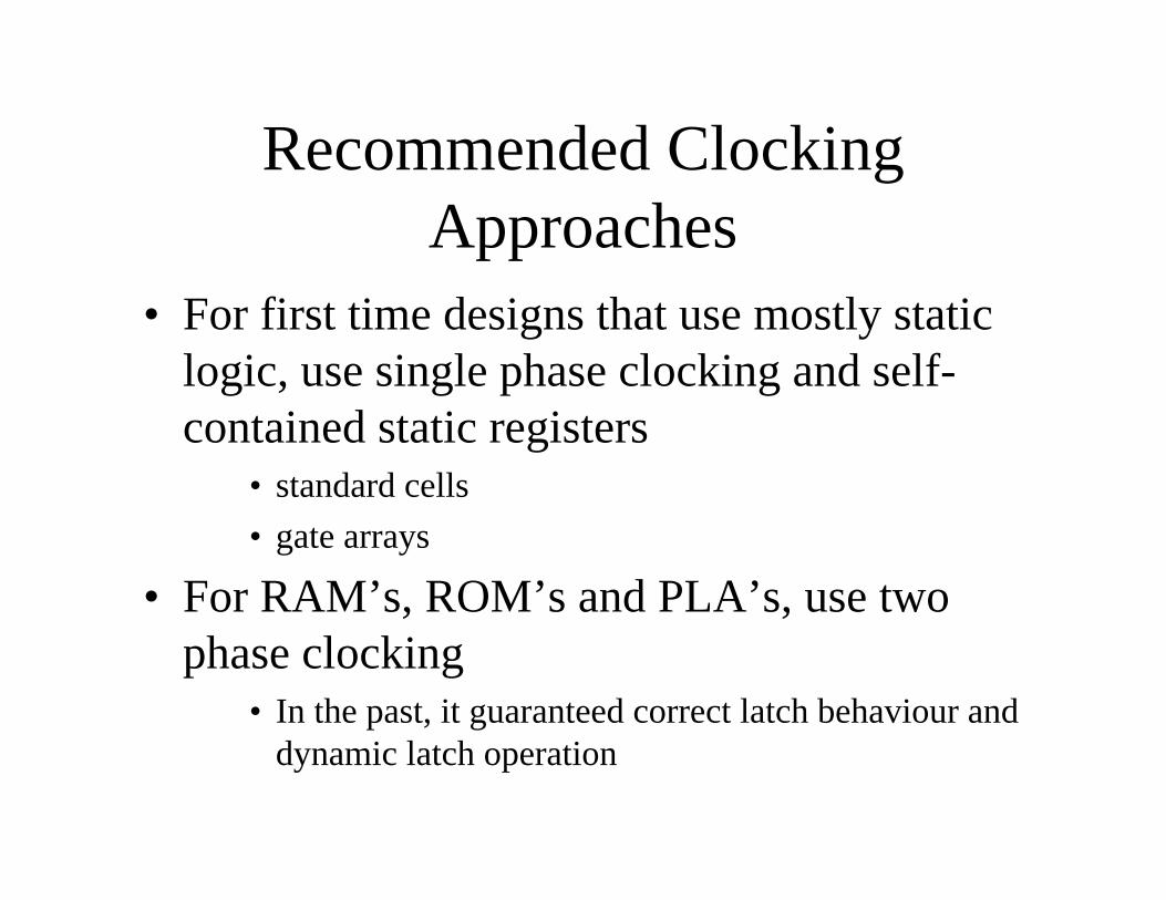
Recommended ClockingApproaches
• For first time designs that use mostly staticlogic, use single phase clocking and self-contained static registers
• standard cells
• gate arrays
• For RAM’s, ROM’s and PLA’s, use twophase clocking
• In the past, it guaranteed correct latch behaviour anddynamic latch operation
Recommended ClockingApproaches (cont.)
• Today, cycle times are very short• difficult to guarantee non-overlap in all process
corners
• Use single phase clocking for complexhigh-speed CMOS circuits
• generate special clock needs locally
• Use alternative clocking schemes only inspecial circumstances
I/O Pads
• design required detailed circuits and processknowledge
• use library functions
• pads have constant height (power connections)
• bonding pad 150µ x 150µ (double bond topower)
Pads (cont.)
• Types of Pads• input
• output
• tristate
• I/O
• VDD
• GND
• analog
• families of pads with different sizes
• ring and core supplies
• multiple supplies for a large number of I/O’s > 40pins 2 sets reduce noise, IR drops
• automatic frame programs to generate pad ring
• resistance and protection diodes are to preventdamage from ESD
• TTL requires switching threshold near 1.4volts
Pads (cont.)
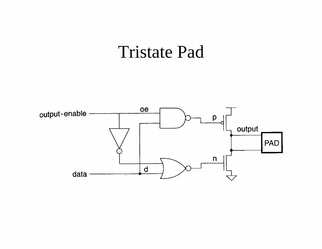
Tristate Pad
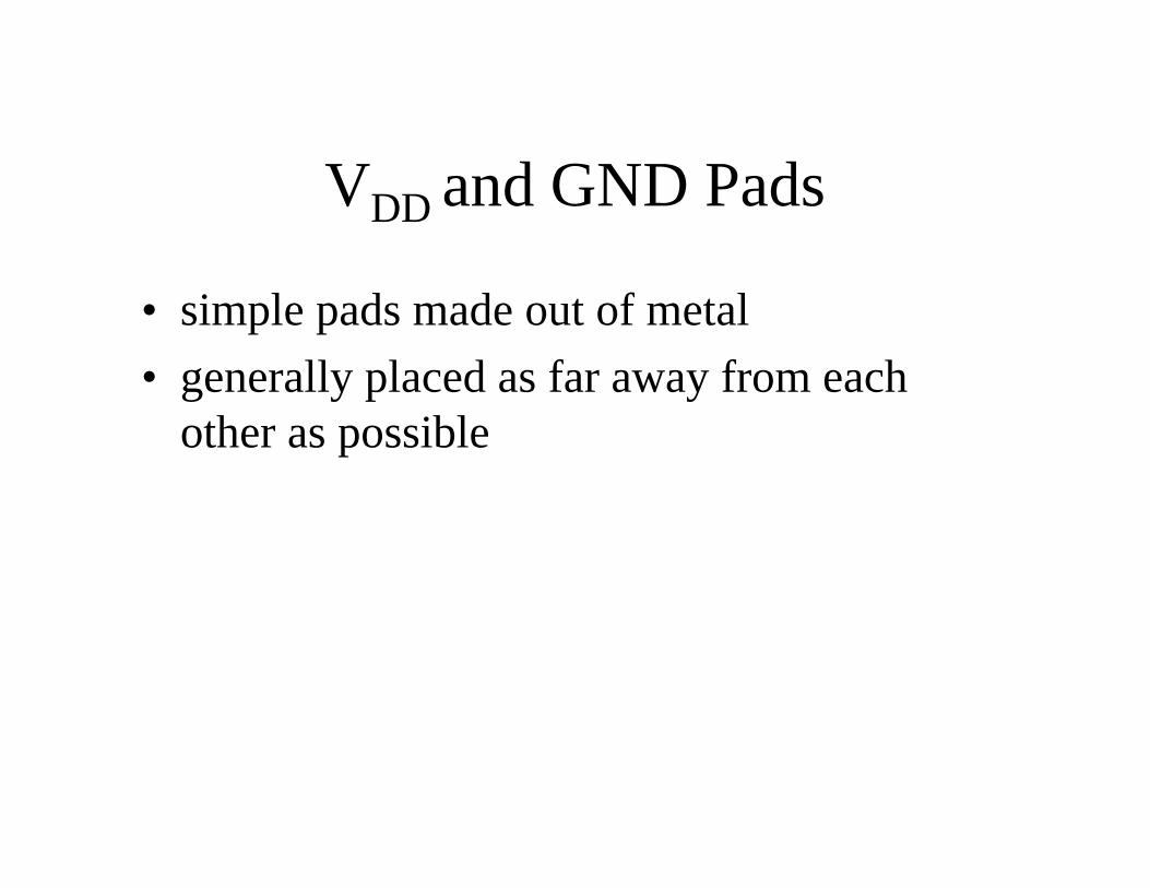
VDD and GND Pads
• simple pads made out of metal
• generally placed as far away from eachother as possible
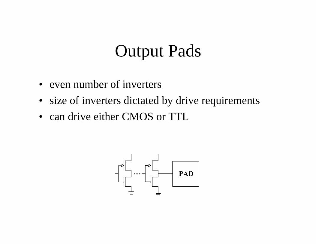
Output Pads
• even number of inverters
• size of inverters dictated by drive requirements
• can drive either CMOS or TTL
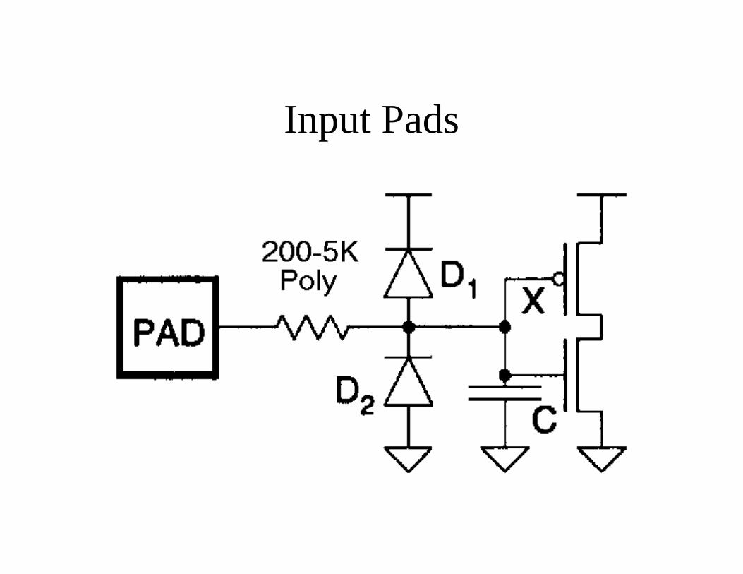
Input Pads