Embed Size (px)
Citation preview
Rev.12.18.17_#1.1
AYA 3W Series
Page 1
Technical Reference Note
AYA 3W Series
3 Watts
DC/DC Converter
Total Power: 3 Watts
Input Voltage: 4.5 to 10 Vdc
9 to 18 Vdc
18 to 36 Vdc
36 to 75 Vdc
# of Outputs: Single /Dual
Special Features• Package size 0.55” x 0.55” x 0.31”
• High efficiency up to 87%
• I/O isolation voltage 1500Vdc
• Ultra-wide 2:1 input range
• Operating temperature range:
-40 OC to +85 OC(with derating)
• 3 Years product warranty
SafetycUL/UL 60950-1
IEC/EN 60950-1
CE Mark
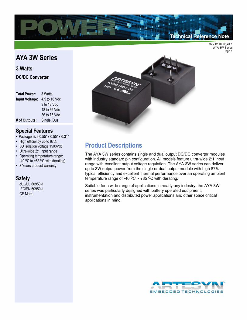
Product DescriptionsThe AYA 3W series contains single and dual output DC/DC converter modules
with industry standard pin configuration. All models feature ultra-wide 2:1 input
range with excellent output voltage regulation. The AYA 3W series can deliver
up to 3W output power from the single or dual output module with high 87%
typical efficiency and excellent thermal performance over an operating ambient
temperature range of -40 OC ~ +85 OC with derating.
Suitable for a wide range of applications in nearly any industry, the AYA 3W
series was particularly designed with battery operated equipment,
instrumentation and distributed power applications and other space critical
applications in mind.
Technical Reference Note
Rev.12.18.17_#1.1
AYA 3W Series
Page 2
Technical Reference Note
Artesyn Embedded Technologies
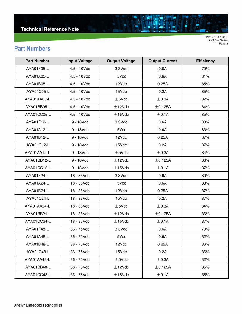
Part Numbers
Part Number Input Voltage Output Voltage Output Current Efficiency
AYA01F05-L 4.5 - 10Vdc 3.3Vdc 0.6A 79%
AYA01A05-L 4.5 - 10Vdc 5Vdc 0.6A 81%
AYA01B05-L 4.5 - 10Vdc 12Vdc 0.25A 85%
AYA01C05-L 4.5 - 10Vdc 15Vdc 0.2A 85%
AYA01AA05-L 4.5 - 10Vdc ±5Vdc ±0.3A 82%
AYA01BB05-L 4.5 - 10Vdc ±12Vdc ±0.125A 84%
AYA01CC05-L 4.5 - 10Vdc ±15Vdc ±0.1A 85%
AYA01F12-L 9 - 18Vdc 3.3Vdc 0.6A 80%
AYA01A12-L 9 - 18Vdc 5Vdc 0.6A 83%
AYA01B12-L 9 - 18Vdc 12Vdc 0.25A 87%
AYA01C12-L 9 - 18Vdc 15Vdc 0.2A 87%
AYA01AA12-L 9 - 18Vdc ±5Vdc ±0.3A 84%
AYA01BB12-L 9 - 18Vdc ±12Vdc ±0.125A 86%
AYA01CC12-L 9 - 18Vdc ±15Vdc ±0.1A 87%
AYA01F24-L 18 - 36Vdc 3.3Vdc 0.6A 80%
AYA01A24-L 18 - 36Vdc 5Vdc 0.6A 83%
AYA01B24-L 18 - 36Vdc 12Vdc 0.25A 87%
AYA01C24-L 18 - 36Vdc 15Vdc 0.2A 87%
AYA01AA24-L 18 - 36Vdc ±5Vdc ±0.3A 84%
AYA01BB24-L 18 - 36Vdc ±12Vdc ±0.125A 86%
AYA01CC24-L 18 - 36Vdc ±15Vdc ±0.1A 87%
AYA01F48-L 36 - 75Vdc 3.3Vdc 0.6A 79%
AYA01A48-L 36 - 75Vdc 5Vdc 0.6A 82%
AYA01B48-L 36 - 75Vdc 12Vdc 0.25A 86%
AYA01C48-L 36 - 75Vdc 15Vdc 0.2A 86%
AYA01AA48-L 36 - 75Vdc ±5Vdc ±0.3A 82%
AYA01BB48-L 36 - 75Vdc ±12Vdc ±0.125A 85%
AYA01CC48-L 36 - 75Vdc ±15Vdc ±0.1A 85%
Technical Reference Note
Rev.12.18.17_#1.1
AYA 3W Series
Page 3
Technical Reference Note
Artesyn Embedded Technologies
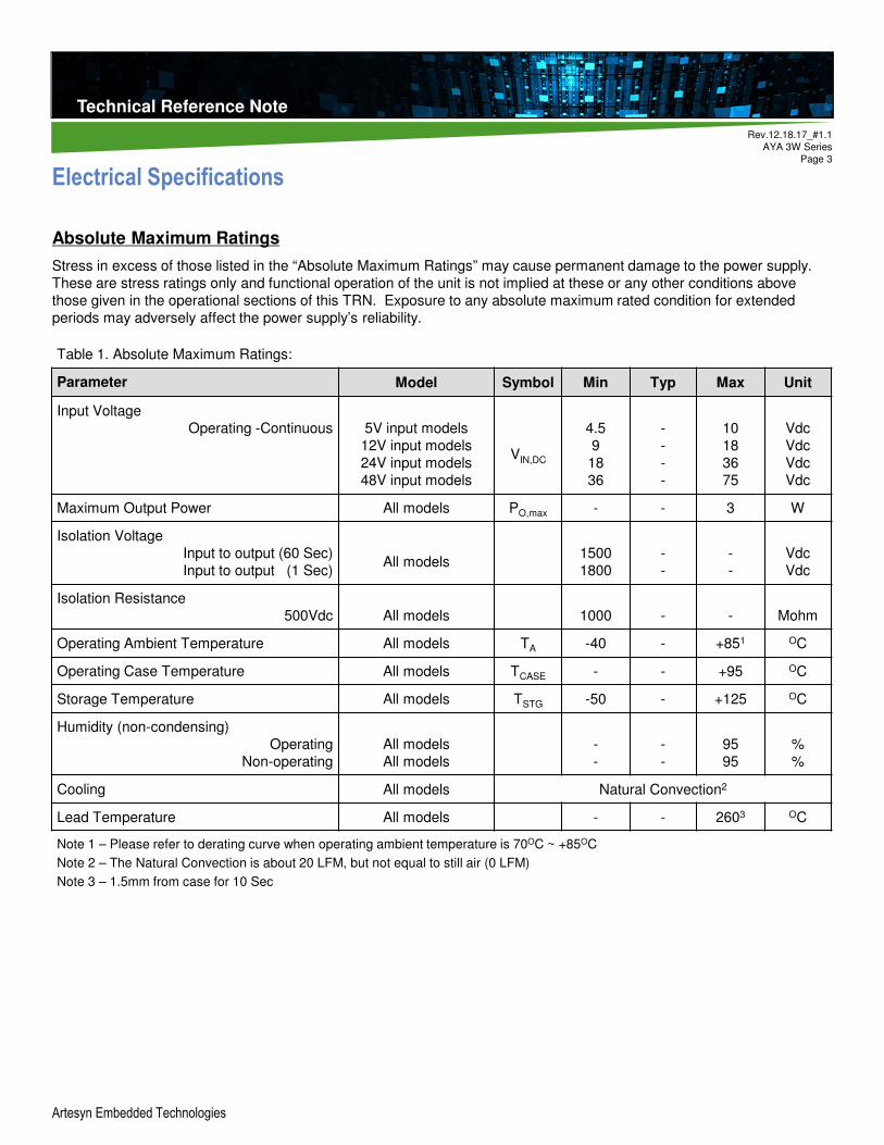
Table 1. Absolute Maximum Ratings:
Parameter Model Symbol Min Typ Max Unit
Input Voltage
Operating -Continuous 5V input models
12V input models
24V input models
48V input models
VIN,DC
4.5
9
18
36
-
-
-
-
10
18
36
75
Vdc
Vdc
Vdc
Vdc
Maximum Output Power All models PO,max - - 3 W
Isolation Voltage
Input to output (60 Sec)
Input to output (1 Sec) All models
1500
1800
-
-
-
-
Vdc
Vdc
Isolation Resistance
500Vdc All models 1000 - - Mohm
Operating Ambient Temperature All models TA -40 - +851 OC
Operating Case Temperature All models TCASE - - +95 OC
Storage Temperature All models TSTG -50 - +125 OC
Humidity (non-condensing)
Operating
Non-operating
All models
All models
-
-
-
-
95
95
%
%
Cooling All models Natural Convection2
Lead Temperature All models - - 2603 OC
Note 1 – Please refer to derating curve when operating ambient temperature is 70OC ~ +85OC
Note 2 – The Natural Convection is about 20 LFM, but not equal to still air (0 LFM)
Note 3 – 1.5mm from case for 10 Sec
Electrical Specifications
Absolute Maximum Ratings
Stress in excess of those listed in the “Absolute Maximum Ratings” may cause permanent damage to the power supply.
These are stress ratings only and functional operation of the unit is not implied at these or any other conditions above
those given in the operational sections of this TRN. Exposure to any absolute maximum rated condition for extended
periods may adversely affect the power supply’s reliability.
Technical Reference Note
Rev.12.18.17_#1.1
AYA 3W Series
Page 4
Technical Reference Note
Artesyn Embedded Technologies
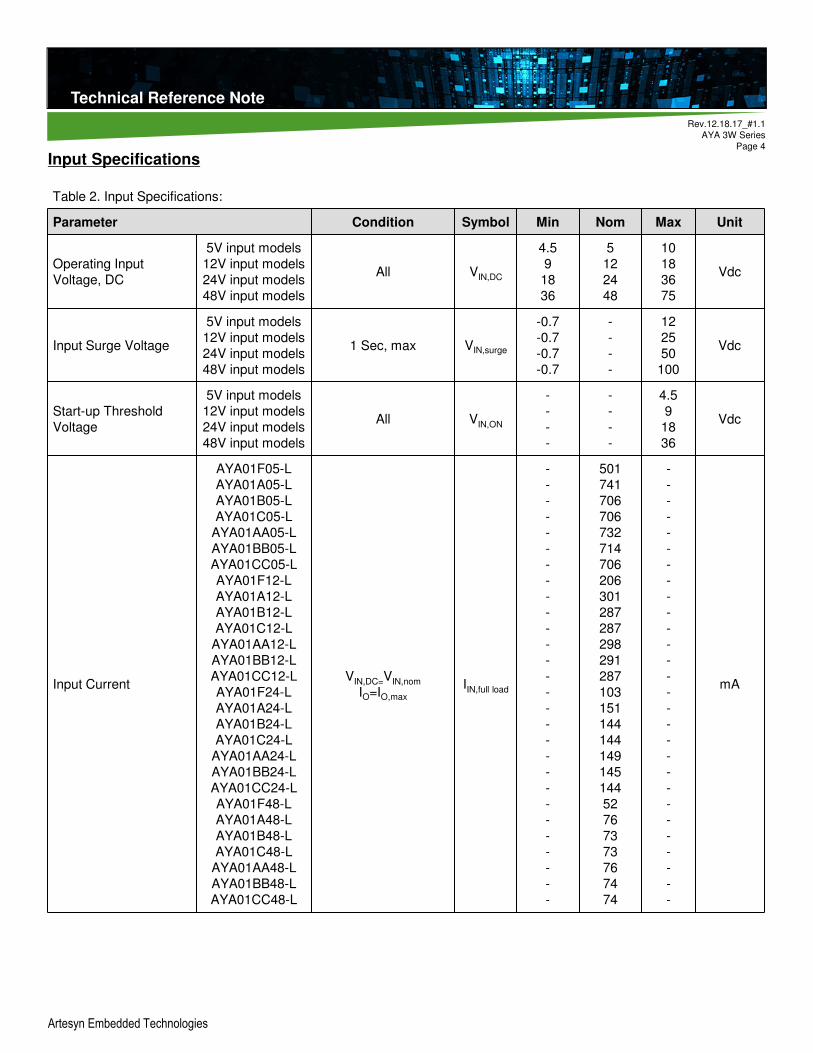
Input Specifications
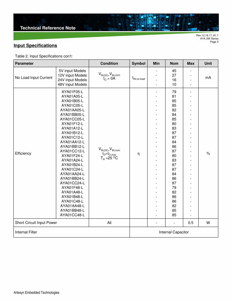
Table 2. Input Specifications:
Parameter Condition Symbol Min Nom Max Unit
Operating Input
Voltage, DC
5V input models
12V input models
24V input models
48V input models
All VIN,DC
4.5
9
18
36
5
12
24
48
10
18
36
75
Vdc
Input Surge Voltage
5V input models
12V input models
24V input models
48V input models
1 Sec, max VIN,surge
-0.7
-0.7
-0.7
-0.7
-
-
-
-
12
25
50
100
Vdc
Start-up Threshold
Voltage
5V input models
12V input models
24V input models
48V input models
All VIN,ON
-
-
-
-
-
-
-
-
4.5
9
18
36
Vdc
Input Current
AYA01F05-L
AYA01A05-L
AYA01B05-L
AYA01C05-L
AYA01AA05-L
AYA01BB05-L
AYA01CC05-L
AYA01F12-L
AYA01A12-L
AYA01B12-L
AYA01C12-L
AYA01AA12-L
AYA01BB12-L
AYA01CC12-L
AYA01F24-L
AYA01A24-L
AYA01B24-L
AYA01C24-L
AYA01AA24-L
AYA01BB24-L
AYA01CC24-L
AYA01F48-L
AYA01A48-L
AYA01B48-L
AYA01C48-L
AYA01AA48-L
AYA01BB48-L
AYA01CC48-L
VIN,DC=VIN,nom
IO=IO,max
IIN,full load
-
-
-
-
-
-
-
-
-
-
-
-
-
-
-
-
-
-
-
-
-
-
-
-
-
-
-
-
501
741
706
706
732
714
706
206
301
287
287
298
291
287
103
151
144
144
149
145
144
52
76
73
73
76
74
74
-
-
-
-
-
-
-
-
-
-
-
-
-
-
-
-
-
-
-
-
-
-
-
-
-
-
-
-
mA
Technical Reference Note
Rev.12.18.17_#1.1
AYA 3W Series
Page 5
Technical Reference Note
Artesyn Embedded Technologies
Input Specifications
Table 2. Input Specifications con’t:
Parameter Condition Symbol Min Nom Max Unit
No Load Input Current
5V input Models
12V input Models
24V input Models
48V input Models
VIN,DC=VIN,nom
IO = 0A IIN,no-load
-
-
-
-
45
27
16
10
-
-
-
-
mA
Efficiency
AYA01F05-L
AYA01A05-L
AYA01B05-L
AYA01C05-L
AYA01AA05-L
AYA01BB05-L
AYA01CC05-L
AYA01F12-L
AYA01A12-L
AYA01B12-L
AYA01C12-L
AYA01AA12-L
AYA01BB12-L
AYA01CC12-L
AYA01F24-L
AYA01A24-L
AYA01B24-L
AYA01C24-L
AYA01AA24-L
AYA01BB24-L
AYA01CC24-L
AYA01F48-L
AYA01A48-L
AYA01B48-L
AYA01C48-L
AYA01AA48-L
AYA01BB48-L
AYA01CC48-L
VIN,DC=VIN,nom
IO=IO,max
TA =25 OC
η
-
-
-
-
-
-
-
-
-
-
-
-
-
-
-
-
-
-
-
-
-
-
-
-
-
-
-
-
79
81
85
85
82
84
85
80
83
87
87
84
86
87
80
83
87
87
84
86
87
79
82
86
86
82
85
85
-
-
-
-
-
-
-
-
-
-
-
-
-
-
-
-
-
-
-
-
-
-
-
-
-
-
-
-
%
Short Circuit Input Power All - - 0.5 W
Internal Filter Internal Capacitor
Technical Reference Note
Rev.12.18.17_#1.1
AYA 3W Series
Page 6
Technical Reference Note
Artesyn Embedded Technologies
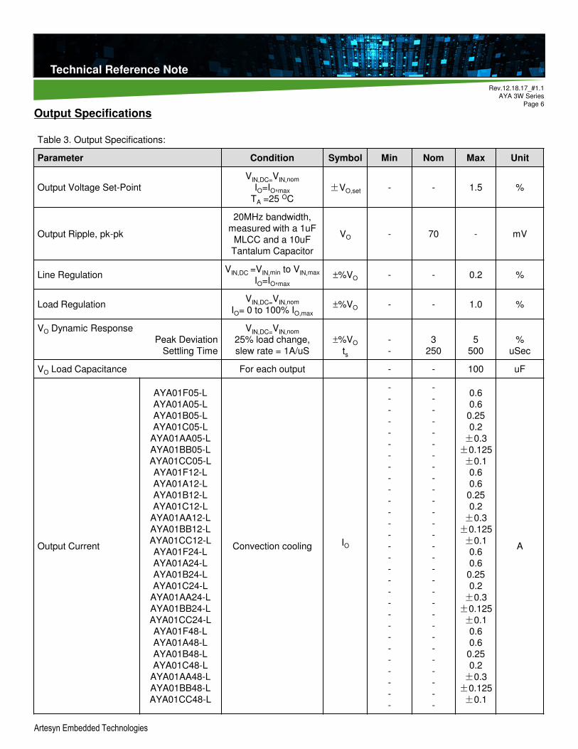
Table 3. Output Specifications:
Parameter Condition Symbol Min Nom Max Unit
Output Voltage Set-Point
VIN,DC=VIN,nom
IO=IO,max
TA =25 OC±VO,set - - 1.5 %
Output Ripple, pk-pk
20MHz bandwidth,
measured with a 1uF
MLCC and a 10uF
Tantalum Capacitor
VO - 70 - mV
Line Regulation VIN,DC =VIN,min to VIN,max
IO=IO,max
±%VO - - 0.2 %
Load RegulationVIN,DC=VIN,nom
IO= 0 to 100% IO,max
±%VO - - 1.0 %
VO Dynamic Response
Peak Deviation
Settling Time
VIN,DC=VIN,nom
25% load change,
slew rate = 1A/uS
±%VO
ts
-
-
3
250
5
500
%
uSec
VO Load Capacitance For each output - - 100 uF
Output Current
AYA01F05-L
AYA01A05-L
AYA01B05-L
AYA01C05-L
AYA01AA05-L
AYA01BB05-L
AYA01CC05-L
AYA01F12-L
AYA01A12-L
AYA01B12-L
AYA01C12-L
AYA01AA12-L
AYA01BB12-L
AYA01CC12-L
AYA01F24-L
AYA01A24-L
AYA01B24-L
AYA01C24-L
AYA01AA24-L
AYA01BB24-L
AYA01CC24-L
AYA01F48-L
AYA01A48-L
AYA01B48-L
AYA01C48-L
AYA01AA48-L
AYA01BB48-L
AYA01CC48-L
Convection cooling IO
-
-
-
-
-
-
-
-
-
-
-
-
-
-
-
-
-
-
-
-
-
-
-
-
-
-
-
-
-
-
-
-
-
-
-
-
-
-
-
-
-
-
-
-
-
-
-
-
-
-
-
-
-
-
-
-
-
-
0.6
0.6
0.25
0.2
±0.3
±0.125
±0.10.6
0.6
0.25
0.2
±0.3
±0.125
±0.10.6
0.6
0.25
0.2
±0.3
±0.125
±0.10.6
0.6
0.25
0.2
±0.3
±0.125
±0.1
A
Output Specifications
Technical Reference Note
Rev.12.18.17_#1.1
AYA 3W Series
Page 7
Technical Reference Note
Artesyn Embedded Technologies
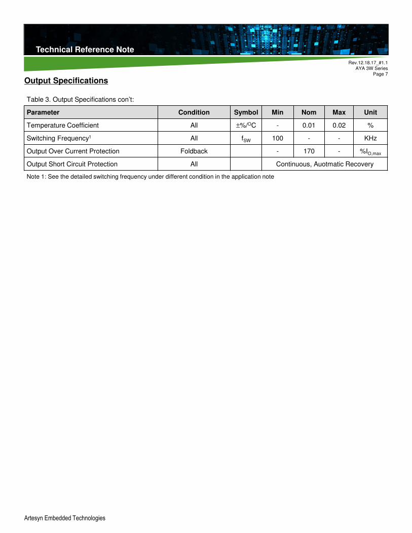
Table 3. Output Specifications con’t:
Parameter Condition Symbol Min Nom Max Unit
Temperature Coefficient All ±%/OC - 0.01 0.02 %
Switching Frequency1 All fSW 100 - - KHz
Output Over Current Protection Foldback - 170 - %IO,max
Output Short Circuit Protection All Continuous, Auotmatic Recovery
Note 1: See the detailed switching frequency under different condition in the application note
Output Specifications
Technical Reference Note
Rev.12.18.17_#1.1
AYA 3W Series
Page 8
Technical Reference Note
Artesyn Embedded Technologies
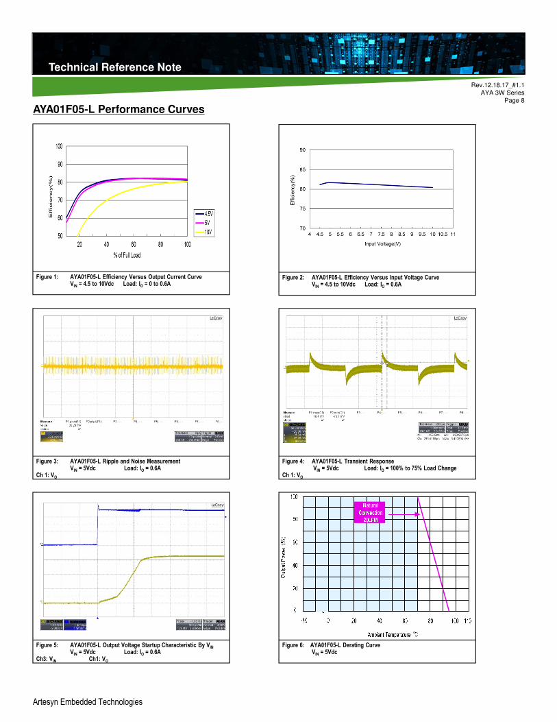
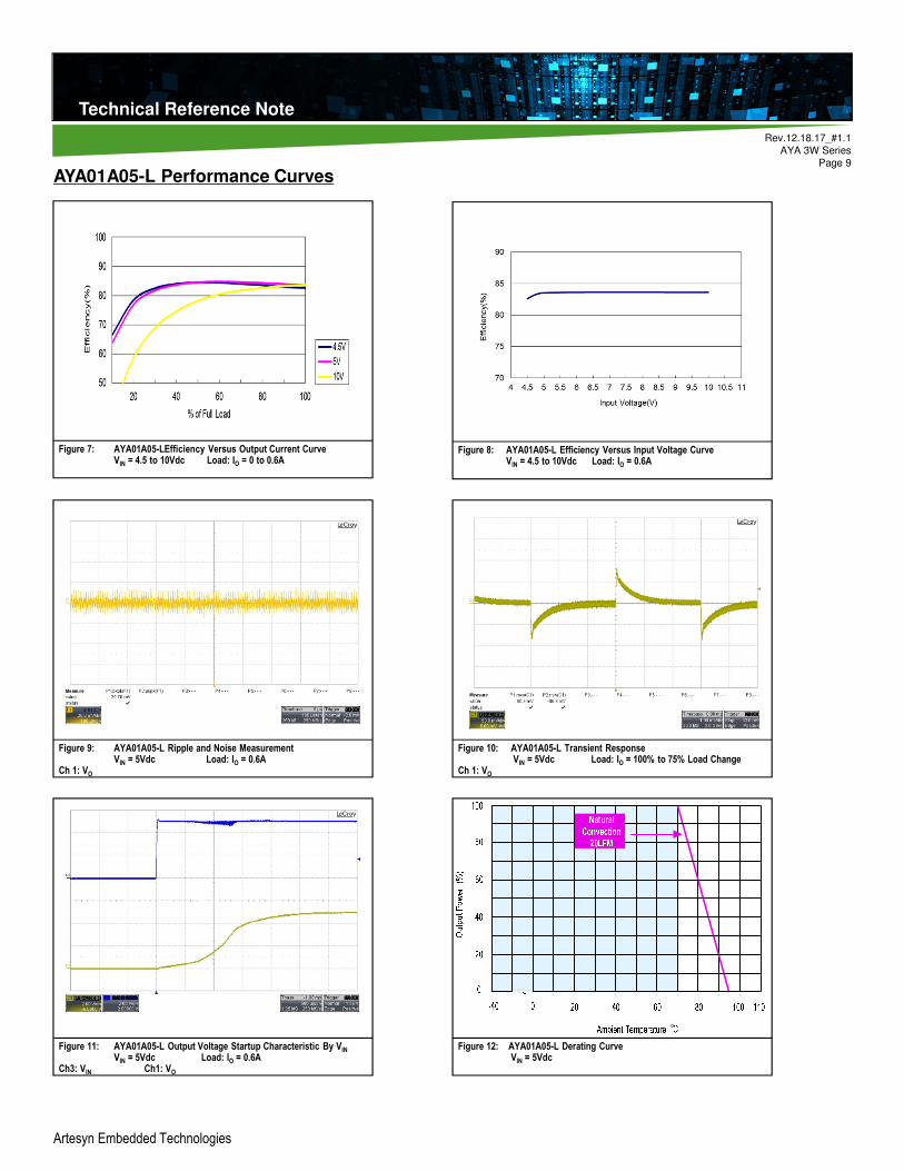
AYA01F05-L Performance Curves
Figure 4: AYA01F05-L Transient ResponseVIN = 5Vdc Load: IO = 100% to 75% Load Change
Ch 1: VO
Figure 1: AYA01F05-L Efficiency Versus Output Current CurveVIN = 4.5 to 10Vdc Load: IO = 0 to 0.6A
Figure 2: AYA01F05-L Efficiency Versus Input Voltage CurveVIN = 4.5 to 10Vdc Load: IO = 0.6A
Figure 3: AYA01F05-L Ripple and Noise MeasurementVIN = 5Vdc Load: IO = 0.6A
Ch 1: VO
Figure 5: AYA01F05-L Output Voltage Startup Characteristic By VIN
VIN = 5Vdc Load: IO = 0.6ACh3: VIN Ch1: VO
Figure 6: AYA01F05-L Derating CurveVIN = 5Vdc
Technical Reference Note
Rev.12.18.17_#1.1
AYA 3W Series
Page 9
Technical Reference Note
Artesyn Embedded Technologies
AYA01A05-L Performance Curves
Figure 10: AYA01A05-L Transient ResponseVIN = 5Vdc Load: IO = 100% to 75% Load Change
Ch 1: VO
Figure 7: AYA01A05-LEfficiency Versus Output Current CurveVIN = 4.5 to 10Vdc Load: IO = 0 to 0.6A
Figure 8: AYA01A05-L Efficiency Versus Input Voltage CurveVIN = 4.5 to 10Vdc Load: IO = 0.6A
Figure 9: AYA01A05-L Ripple and Noise MeasurementVIN = 5Vdc Load: IO = 0.6A
Ch 1: VO
Figure 11: AYA01A05-L Output Voltage Startup Characteristic By VIN
VIN = 5Vdc Load: IO = 0.6ACh3: VIN Ch1: VO
Figure 12: AYA01A05-L Derating CurveVIN = 5Vdc
Technical Reference Note
Rev.12.18.17_#1.1
AYA 3W Series
Page 10
Technical Reference Note
Artesyn Embedded Technologies
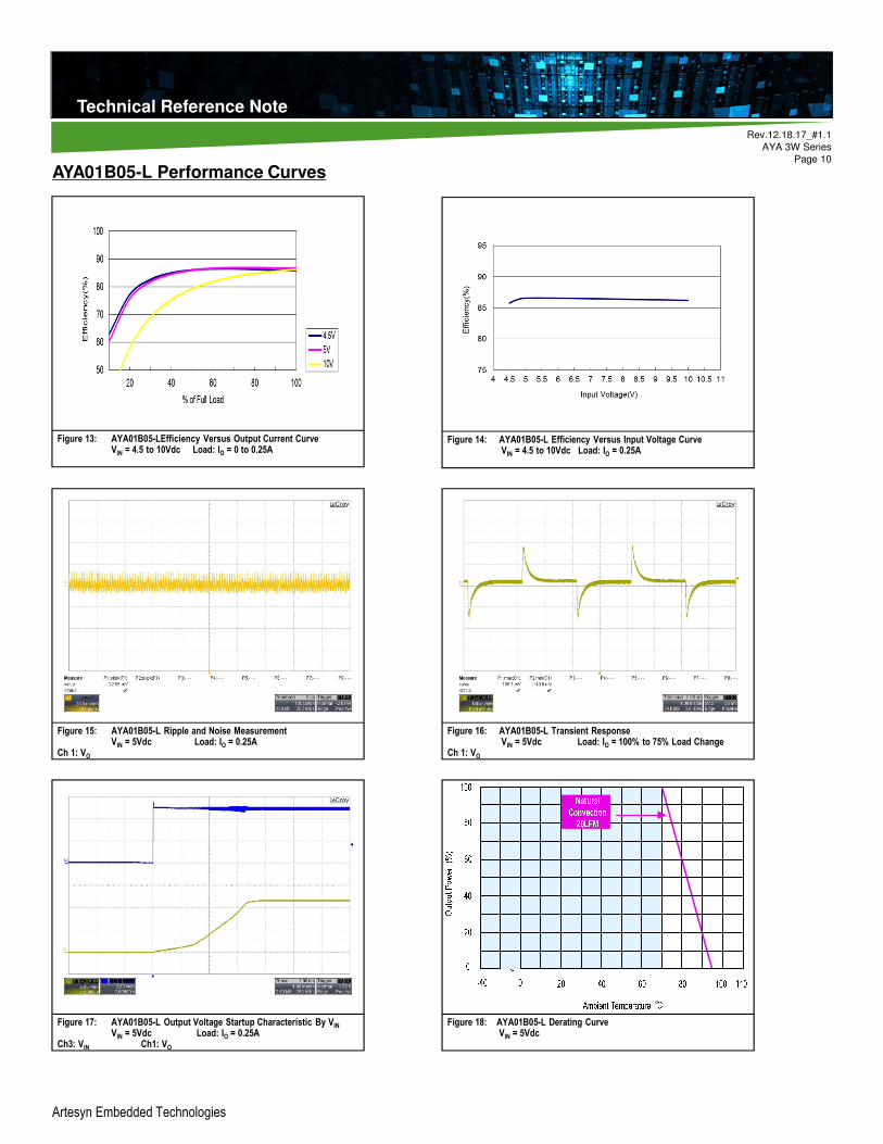
AYA01B05-L Performance Curves
Figure 16: AYA01B05-L Transient ResponseVIN = 5Vdc Load: IO = 100% to 75% Load Change
Ch 1: VO
Figure 13: AYA01B05-LEfficiency Versus Output Current CurveVIN = 4.5 to 10Vdc Load: IO = 0 to 0.25A
Figure 14: AYA01B05-L Efficiency Versus Input Voltage CurveVIN = 4.5 to 10Vdc Load: IO = 0.25A
Figure 15: AYA01B05-L Ripple and Noise MeasurementVIN = 5Vdc Load: IO = 0.25A
Ch 1: VO
Figure 17: AYA01B05-L Output Voltage Startup Characteristic By VIN
VIN = 5Vdc Load: IO = 0.25ACh3: VIN Ch1: VO
Figure 18: AYA01B05-L Derating CurveVIN = 5Vdc
AYA01B05-L Performance Curves
Technical Reference Note
Rev.12.18.17_#1.1
AYA 3W Series
Page 11
Technical Reference Note
Artesyn Embedded Technologies
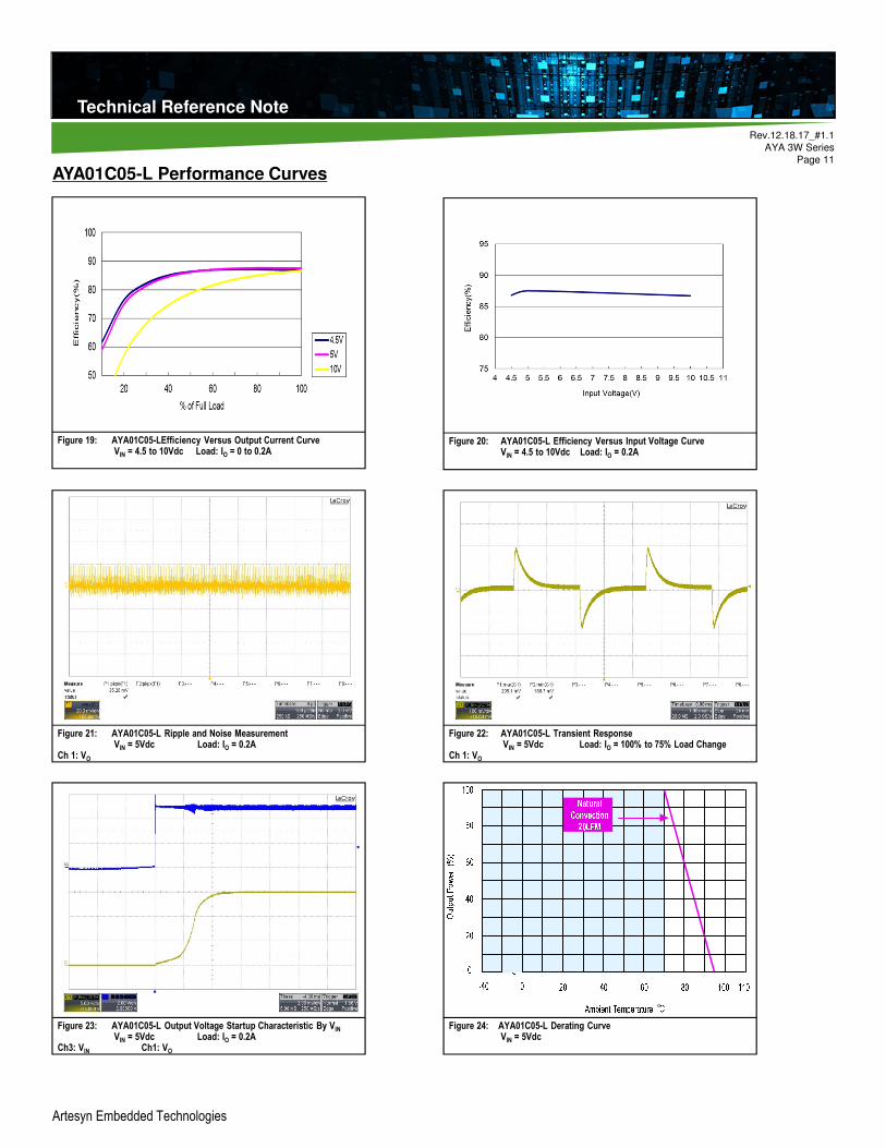
AYA01C05-L Performance Curves
Figure 22: AYA01C05-L Transient ResponseVIN = 5Vdc Load: IO = 100% to 75% Load Change
Ch 1: VO
Figure 19: AYA01C05-LEfficiency Versus Output Current CurveVIN = 4.5 to 10Vdc Load: IO = 0 to 0.2A
Figure 20: AYA01C05-L Efficiency Versus Input Voltage CurveVIN = 4.5 to 10Vdc Load: IO = 0.2A
Figure 21: AYA01C05-L Ripple and Noise MeasurementVIN = 5Vdc Load: IO = 0.2A
Ch 1: VO
Figure 23: AYA01C05-L Output Voltage Startup Characteristic By VIN
VIN = 5Vdc Load: IO = 0.2ACh3: VIN Ch1: VO
Figure 24: AYA01C05-L Derating CurveVIN = 5Vdc
Technical Reference Note
Rev.12.18.17_#1.1
AYA 3W Series
Page 12
Technical Reference Note
Artesyn Embedded Technologies
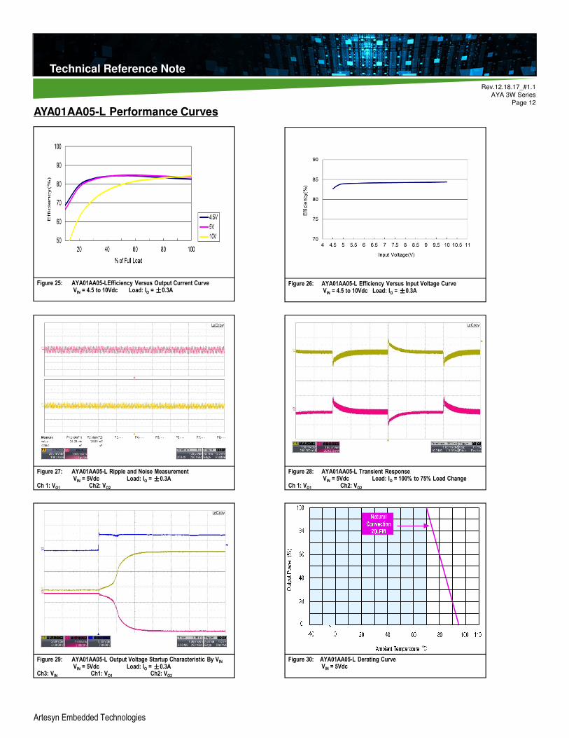
AYA01AA05-L Performance Curves
Figure 28: AYA01AA05-L Transient ResponseVIN = 5Vdc Load: IO = 100% to 75% Load Change
Ch 1: VO1 Ch2: VO2
Figure 25: AYA01AA05-LEfficiency Versus Output Current CurveVIN = 4.5 to 10Vdc Load: IO = ±±±±0.3A
Figure 26: AYA01AA05-L Efficiency Versus Input Voltage CurveVIN = 4.5 to 10Vdc Load: IO = ±±±±0.3A
Figure 27: AYA01AA05-L Ripple and Noise MeasurementVIN = 5Vdc Load: IO = ±±±±0.3A
Ch 1: VO1 Ch2: VO2
Figure 29: AYA01AA05-L Output Voltage Startup Characteristic By VIN
VIN = 5Vdc Load: IO = ±±±±0.3ACh3: VIN Ch1: VO1 Ch2: VO2
Figure 30: AYA01AA05-L Derating CurveVIN = 5Vdc

Technical Reference Note
Rev.12.18.17_#1.1
AYA 3W Series
Page 13
Technical Reference Note
Artesyn Embedded Technologies
AYA01BB05-L Performance Curves
Figure 34: AYA01BB05-L Transient ResponseVIN = 5Vdc Load: IO = 100% to 75% Load Change
Ch 1: VO1 Ch2: VO2
Figure 31: AYA01BB05-L Efficiency Versus Output Current CurveVIN = 4.5 to 10Vdc Load: IO = ±±±±0.125A
Figure 32: AYA01BB05-L Efficiency Versus Input Voltage CurveVIN = 4.5 to 10Vdc Load: IO = ±±±±0.125A
Figure 33: AYA01BB05-L Ripple and Noise MeasurementVIN = 5Vdc Load: IO = ±±±±0.125A
Ch 1: VO1 Ch2: VO2
Figure 35: AYA01BB05-L Output Voltage Startup Characteristic By VIN
VIN = 5Vdc Load: IO = ±±±±0.125ACh3: VIN Ch1: VO1 Ch2: VO2
Figure 36: AYA01BB05-L Derating CurveVIN = 5Vdc
Technical Reference Note
Rev.12.18.17_#1.1
AYA 3W Series
Page 14
Technical Reference Note
Artesyn Embedded Technologies
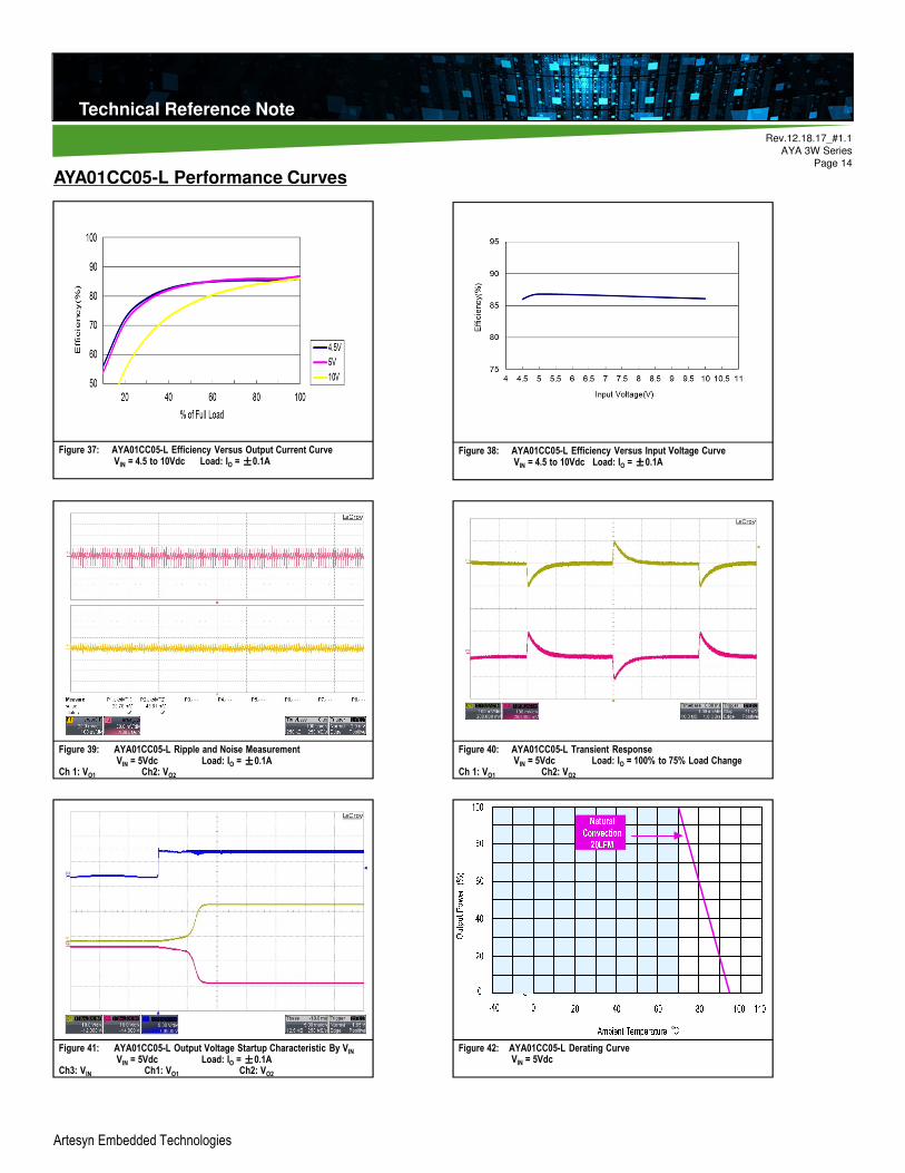
AYA01CC05-L Performance Curves
Figure 40: AYA01CC05-L Transient ResponseVIN = 5Vdc Load: IO = 100% to 75% Load Change
Ch 1: VO1 Ch2: VO2
Figure 37: AYA01CC05-L Efficiency Versus Output Current CurveVIN = 4.5 to 10Vdc Load: IO = ±±±±0.1A
Figure 38: AYA01CC05-L Efficiency Versus Input Voltage CurveVIN = 4.5 to 10Vdc Load: IO = ±±±±0.1A
Figure 39: AYA01CC05-L Ripple and Noise MeasurementVIN = 5Vdc Load: IO = ±±±±0.1A
Ch 1: VO1 Ch2: VO2
Figure 41: AYA01CC05-L Output Voltage Startup Characteristic By VIN
VIN = 5Vdc Load: IO = ±±±±0.1ACh3: VIN Ch1: VO1 Ch2: VO2
Figure 42: AYA01CC05-L Derating CurveVIN = 5Vdc
Technical Reference Note
Rev.12.18.17_#1.1
AYA 3W Series
Page 15
Technical Reference Note
Artesyn Embedded Technologies
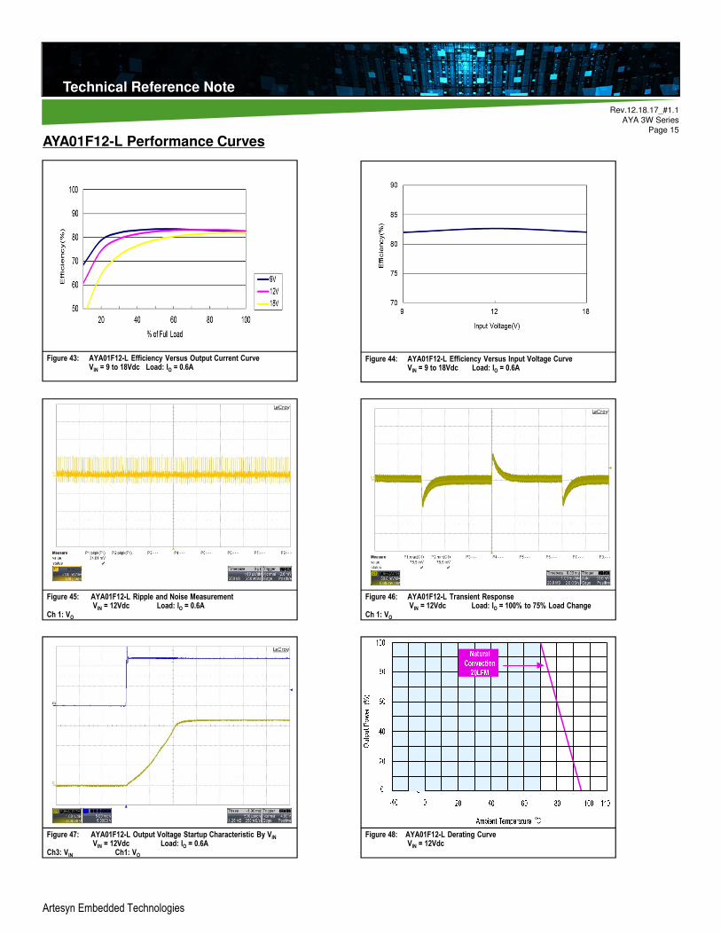
AYA01F12-L Performance Curves
Figure 46: AYA01F12-L Transient ResponseVIN = 12Vdc Load: IO = 100% to 75% Load Change
Ch 1: VO
Figure 43: AYA01F12-L Efficiency Versus Output Current CurveVIN = 9 to 18Vdc Load: IO = 0.6A
Figure 44: AYA01F12-L Efficiency Versus Input Voltage CurveVIN = 9 to 18Vdc Load: IO = 0.6A
Figure 45: AYA01F12-L Ripple and Noise MeasurementVIN = 12Vdc Load: IO = 0.6A
Ch 1: VO
Figure 47: AYA01F12-L Output Voltage Startup Characteristic By VIN
VIN = 12Vdc Load: IO = 0.6ACh3: VIN Ch1: VO
Figure 48: AYA01F12-L Derating CurveVIN = 12Vdc

Technical Reference Note
Rev.12.18.17_#1.1
AYA 3W Series
Page 16
Technical Reference Note
Artesyn Embedded Technologies
AYA01A12-L Performance Curves
Figure 52: AYA01A12-L Transient ResponseVIN = 12Vdc Load: IO = 100% to 75% Load Change
Ch 1: VO
Figure 49: AYA01A12-L Efficiency Versus Output Current CurveVIN = 9 to 18Vdc Load: IO = 0.6A
Figure 50: AYA01A12-L Efficiency Versus Input Voltage CurveVIN = 9 to 18Vdc Load: IO = 0.6A
Figure 51: AYA01A12-L Ripple and Noise MeasurementVIN = 12Vdc Load: IO = 0.6A
Ch 1: VO
Figure 53: AYA01A12-L Output Voltage Startup Characteristic By VIN
VIN = 12Vdc Load: IO = 0.6ACh3: VIN Ch1: VO
Figure 54: AYA01A12-L Derating CurveVIN = 12Vdc
Technical Reference Note
Rev.12.18.17_#1.1
AYA 3W Series
Page 17
Technical Reference Note
Artesyn Embedded Technologies
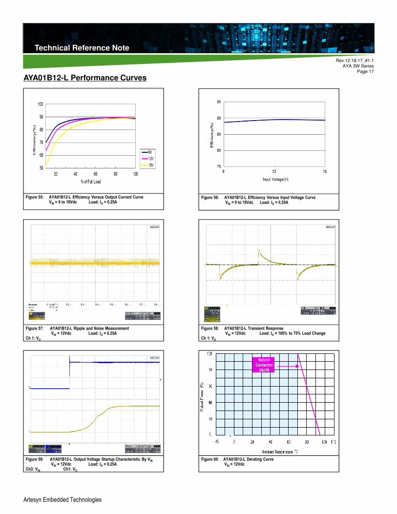
AYA01B12-L Performance Curves
Figure 58: AYA01B12-L Transient ResponseVIN = 12Vdc Load: IO = 100% to 75% Load Change
Ch 1: VO
Figure 55: AYA01B12-L Efficiency Versus Output Current CurveVIN = 9 to 18Vdc Load: IO = 0.25A
Figure 56: AYA01B12-L Efficiency Versus Input Voltage CurveVIN = 9 to 18Vdc Load: IO = 0.25A
Figure 57: AYA01B12-L Ripple and Noise MeasurementVIN = 12Vdc Load: IO = 0.25A
Ch 1: VO
Figure 59: AYA01B12-L Output Voltage Startup Characteristic By VIN
VIN = 12Vdc Load: IO = 0.25ACh3: VIN Ch1: VO
Figure 60: AYA01B12-L Derating CurveVIN = 12Vdc
Technical Reference Note
Rev.12.18.17_#1.1
AYA 3W Series
Page 18
Technical Reference Note
Artesyn Embedded Technologies
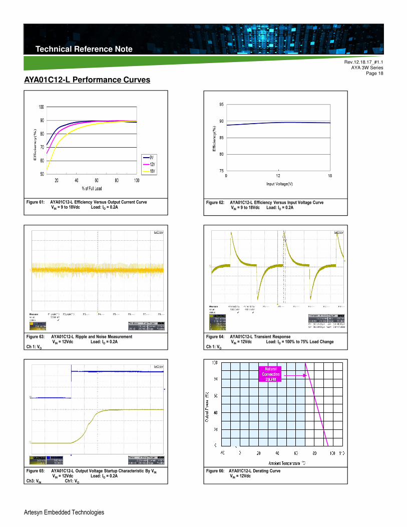
AYA01C12-L Performance Curves
Figure 64: AYA01C12-L Transient ResponseVIN = 12Vdc Load: IO = 100% to 75% Load Change
Ch 1: VO
Figure 61: AYA01C12-L Efficiency Versus Output Current CurveVIN = 9 to 18Vdc Load: IO = 0.2A
Figure 62: AYA01C12-L Efficiency Versus Input Voltage CurveVIN = 9 to 18Vdc Load: IO = 0.2A
Figure 63: AYA01C12-L Ripple and Noise MeasurementVIN = 12Vdc Load: IO = 0.2A
Ch 1: VO
Figure 65: AYA01C12-L Output Voltage Startup Characteristic By VIN
VIN = 12Vdc Load: IO = 0.2ACh3: VIN Ch1: VO
Figure 66: AYA01C12-L Derating CurveVIN = 12Vdc
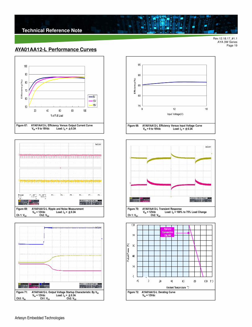
Technical Reference Note
Rev.12.18.17_#1.1
AYA 3W Series
Page 19
Technical Reference Note
Artesyn Embedded Technologies
AYA01AA12-L Performance Curves
Figure 70: AYA01AA12-L Transient ResponseVIN = 12Vdc Load: IO = 100% to 75% Load Change
Ch 1: VO1 Ch2: VO2
Figure 67: AYA01AA12-L Efficiency Versus Output Current CurveVIN = 9 to 18Vdc Load: IO = ±±±±0.3A
Figure 68: AYA01AA12-L Efficiency Versus Input Voltage CurveVIN = 9 to 18Vdc Load: IO = ±±±±0.3A
Figure 69: AYA01AA12-L Ripple and Noise MeasurementVIN = 12Vdc Load: IO = ±±±±0.3A
Ch 1: VO1 Ch2: VO2
Figure 71: AYA01AA12-L Output Voltage Startup Characteristic By VIN
VIN = 12Vdc Load: IO = ±±±±0.3ACh3: VIN Ch1: VO1 Ch2: VO2
Figure 72: AYA01AA12-L Derating CurveVIN = 12Vdc
Technical Reference Note
Rev.12.18.17_#1.1
AYA 3W Series
Page 20
Technical Reference Note
Artesyn Embedded Technologies
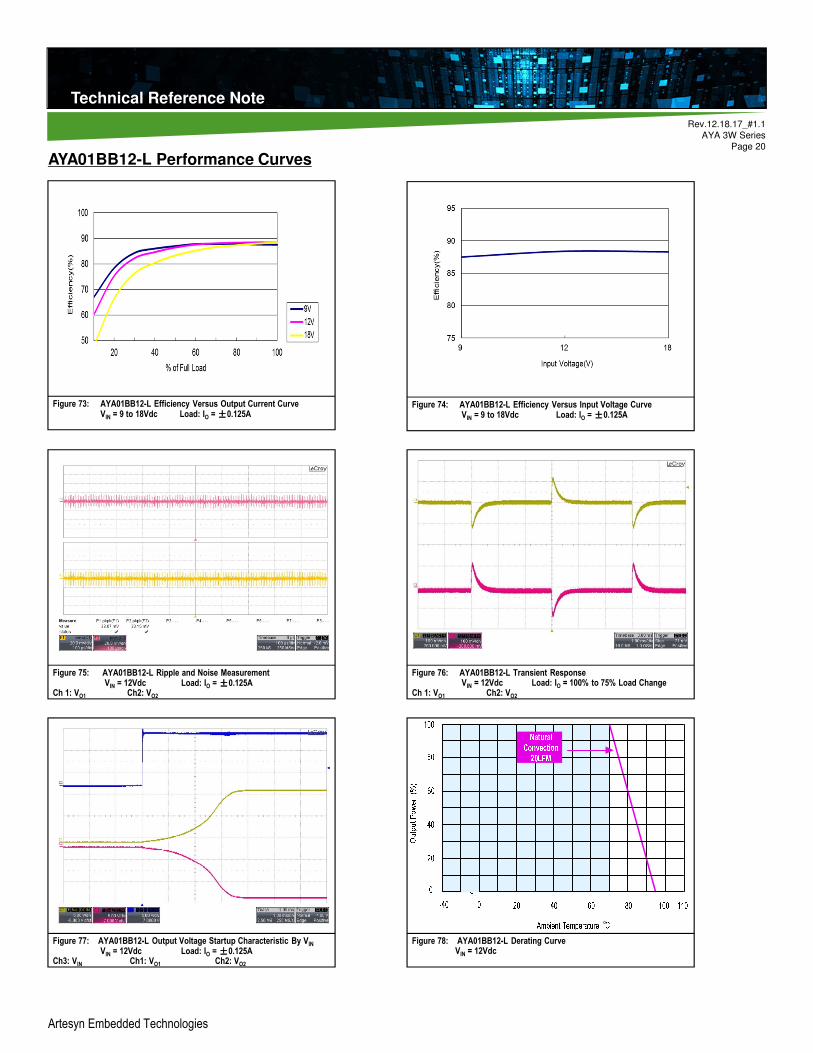
AYA01BB12-L Performance Curves
Figure 76: AYA01BB12-L Transient ResponseVIN = 12Vdc Load: IO = 100% to 75% Load Change
Ch 1: VO1 Ch2: VO2
Figure 73: AYA01BB12-L Efficiency Versus Output Current CurveVIN = 9 to 18Vdc Load: IO = ±±±±0.125A
Figure 74: AYA01BB12-L Efficiency Versus Input Voltage CurveVIN = 9 to 18Vdc Load: IO = ±±±±0.125A
Figure 75: AYA01BB12-L Ripple and Noise MeasurementVIN = 12Vdc Load: IO = ±±±±0.125A
Ch 1: VO1 Ch2: VO2
Figure 77: AYA01BB12-L Output Voltage Startup Characteristic By VIN
VIN = 12Vdc Load: IO = ±±±±0.125ACh3: VIN Ch1: VO1 Ch2: VO2
Figure 78: AYA01BB12-L Derating CurveVIN = 12Vdc
Technical Reference Note
Rev.12.18.17_#1.1
AYA 3W Series
Page 21
Technical Reference Note
Artesyn Embedded Technologies
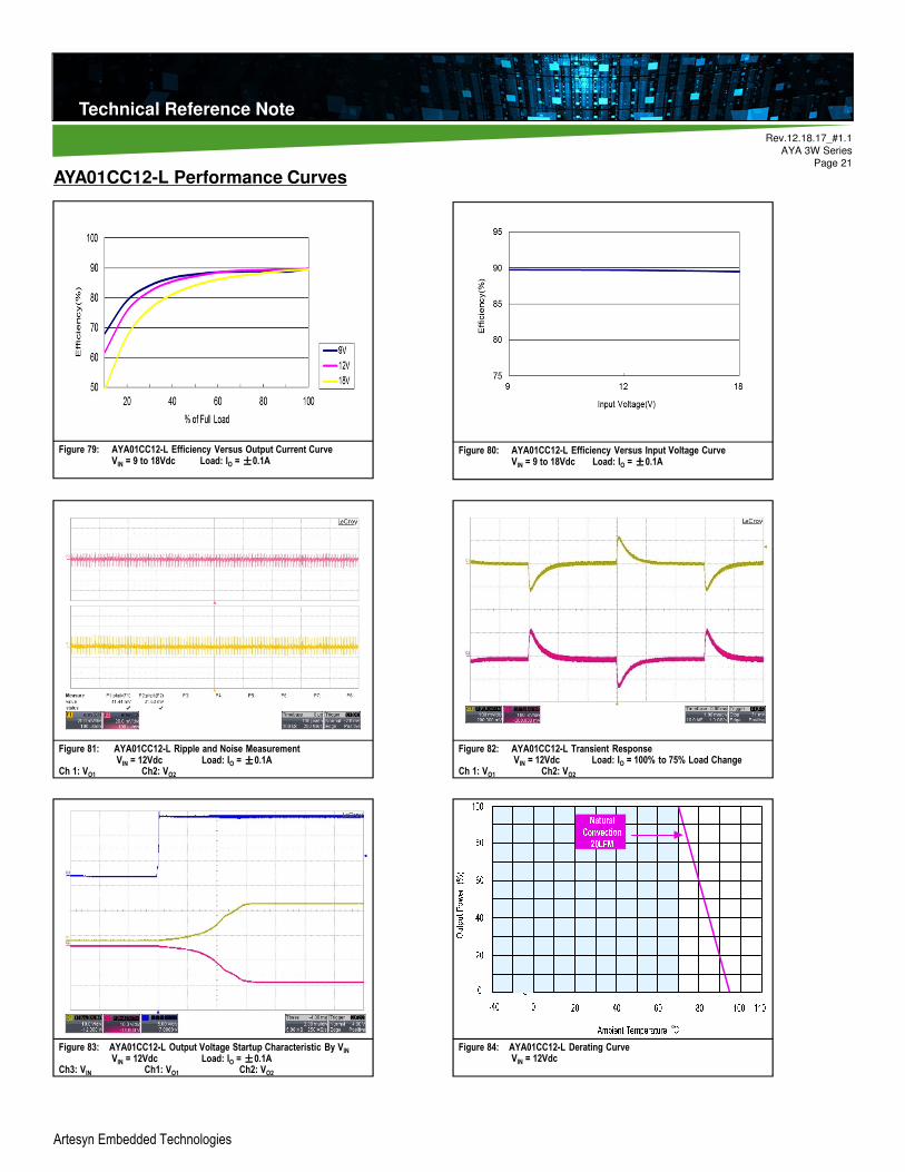
AYA01CC12-L Performance Curves
Figure 82: AYA01CC12-L Transient ResponseVIN = 12Vdc Load: IO = 100% to 75% Load Change
Ch 1: VO1 Ch2: VO2
Figure 79: AYA01CC12-L Efficiency Versus Output Current CurveVIN = 9 to 18Vdc Load: IO = ±±±±0.1A
Figure 80: AYA01CC12-L Efficiency Versus Input Voltage CurveVIN = 9 to 18Vdc Load: IO = ±±±±0.1A
Figure 81: AYA01CC12-L Ripple and Noise MeasurementVIN = 12Vdc Load: IO = ±±±±0.1A
Ch 1: VO1 Ch2: VO2
Figure 83: AYA01CC12-L Output Voltage Startup Characteristic By VIN
VIN = 12Vdc Load: IO = ±±±±0.1ACh3: VIN Ch1: VO1 Ch2: VO2
Figure 84: AYA01CC12-L Derating CurveVIN = 12Vdc
Technical Reference Note
Rev.12.18.17_#1.1
AYA 3W Series
Page 22
Technical Reference Note
Artesyn Embedded Technologies
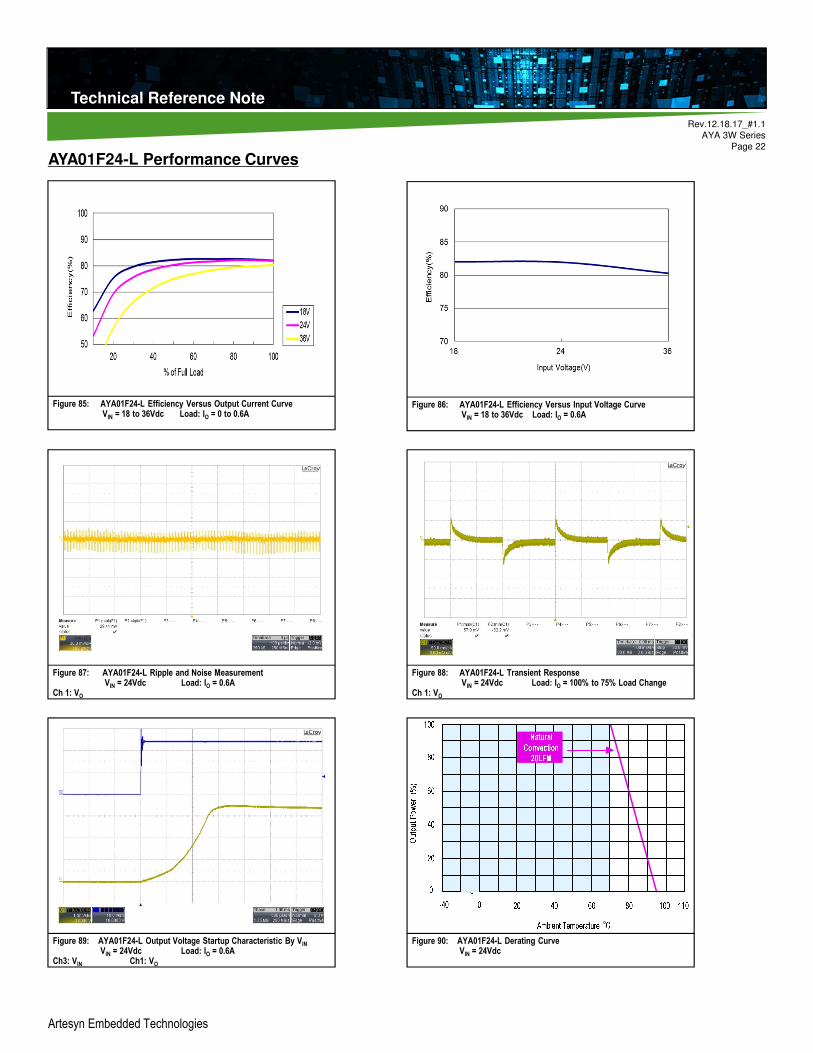
AYA01F24-L Performance Curves
Figure 88: AYA01F24-L Transient ResponseVIN = 24Vdc Load: IO = 100% to 75% Load Change
Ch 1: VO
Figure 85: AYA01F24-L Efficiency Versus Output Current CurveVIN = 18 to 36Vdc Load: IO = 0 to 0.6A
Figure 86: AYA01F24-L Efficiency Versus Input Voltage CurveVIN = 18 to 36Vdc Load: IO = 0.6A
Figure 87: AYA01F24-L Ripple and Noise MeasurementVIN = 24Vdc Load: IO = 0.6A
Ch 1: VO
Figure 89: AYA01F24-L Output Voltage Startup Characteristic By VIN
VIN = 24Vdc Load: IO = 0.6ACh3: VIN Ch1: VO
Figure 90: AYA01F24-L Derating CurveVIN = 24Vdc

Technical Reference Note
Rev.12.18.17_#1.1
AYA 3W Series
Page 23
Technical Reference Note
Artesyn Embedded Technologies
AYA01A24-L Performance Curves
Figure 94: AYA01A24-L Transient ResponseVIN = 24Vdc Load: IO = 100% to 75% Load Change
Ch 1: VO
Figure 91: AYA01A24-L Efficiency Versus Output Current CurveVIN = 18 to 36Vdc Load: IO = 0 to 0.6A
Figure 92: AYA01A24-L Efficiency Versus Input Voltage CurveVIN = 18 to 36Vdc Load: IO = 0.6A
Figure 93: AYA01A24-L Ripple and Noise MeasurementVIN = 24Vdc Load: IO = 0.6A
Ch 1: VO
Figure 95: AYA01A24-L Output Voltage Startup Characteristic By VIN
VIN = 24Vdc Load: IO = 0.6ACh3: VIN Ch1: VO
Figure 96: AYA01A24-L Derating CurveVIN = 24Vdc
Technical Reference Note
Rev.12.18.17_#1.1
AYA 3W Series
Page 24
Technical Reference Note
Artesyn Embedded Technologies
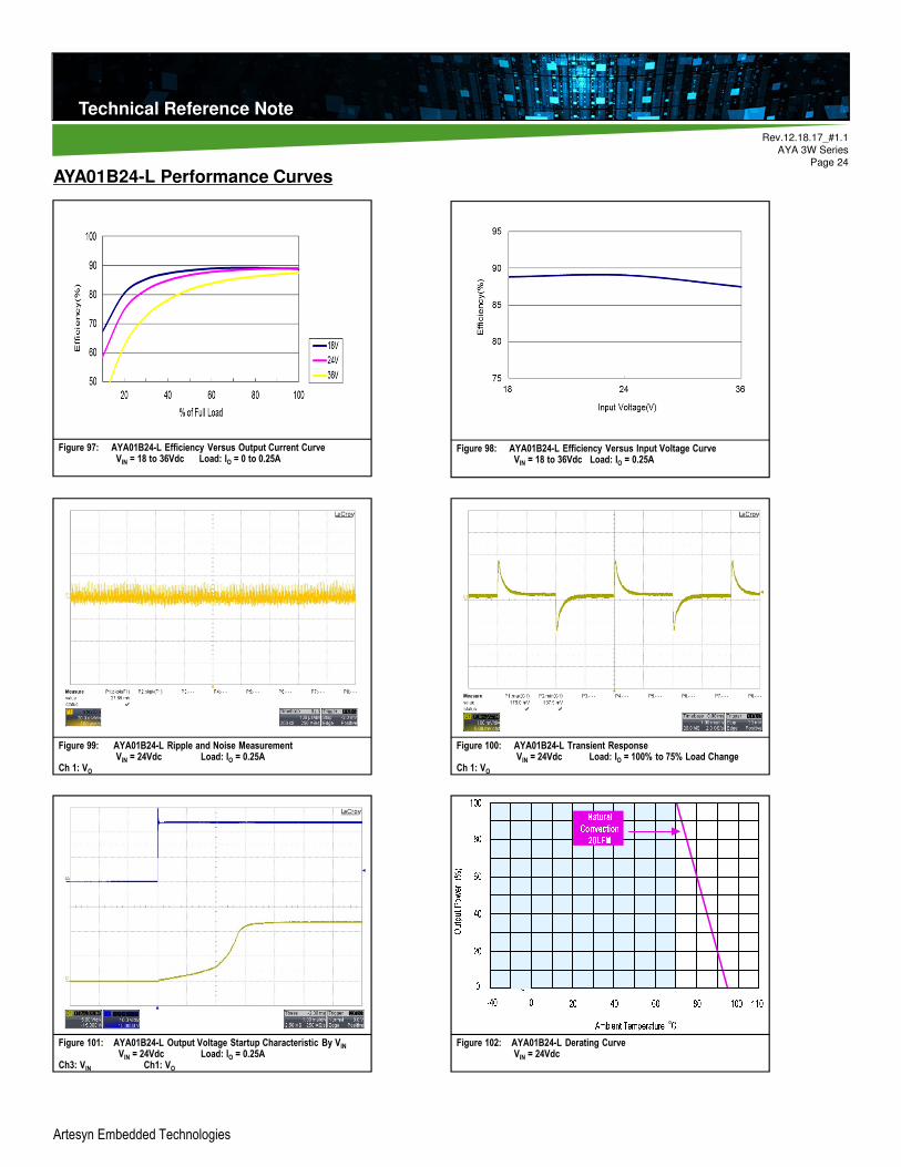
AYA01B24-L Performance Curves
Figure 100: AYA01B24-L Transient ResponseVIN = 24Vdc Load: IO = 100% to 75% Load Change
Ch 1: VO
Figure 97: AYA01B24-L Efficiency Versus Output Current CurveVIN = 18 to 36Vdc Load: IO = 0 to 0.25A
Figure 98: AYA01B24-L Efficiency Versus Input Voltage CurveVIN = 18 to 36Vdc Load: IO = 0.25A
Figure 99: AYA01B24-L Ripple and Noise MeasurementVIN = 24Vdc Load: IO = 0.25A
Ch 1: VO
Figure 101: AYA01B24-L Output Voltage Startup Characteristic By VIN
VIN = 24Vdc Load: IO = 0.25ACh3: VIN Ch1: VO
Figure 102: AYA01B24-L Derating CurveVIN = 24Vdc
Technical Reference Note
Rev.12.18.17_#1.1
AYA 3W Series
Page 25
Technical Reference Note
Artesyn Embedded Technologies
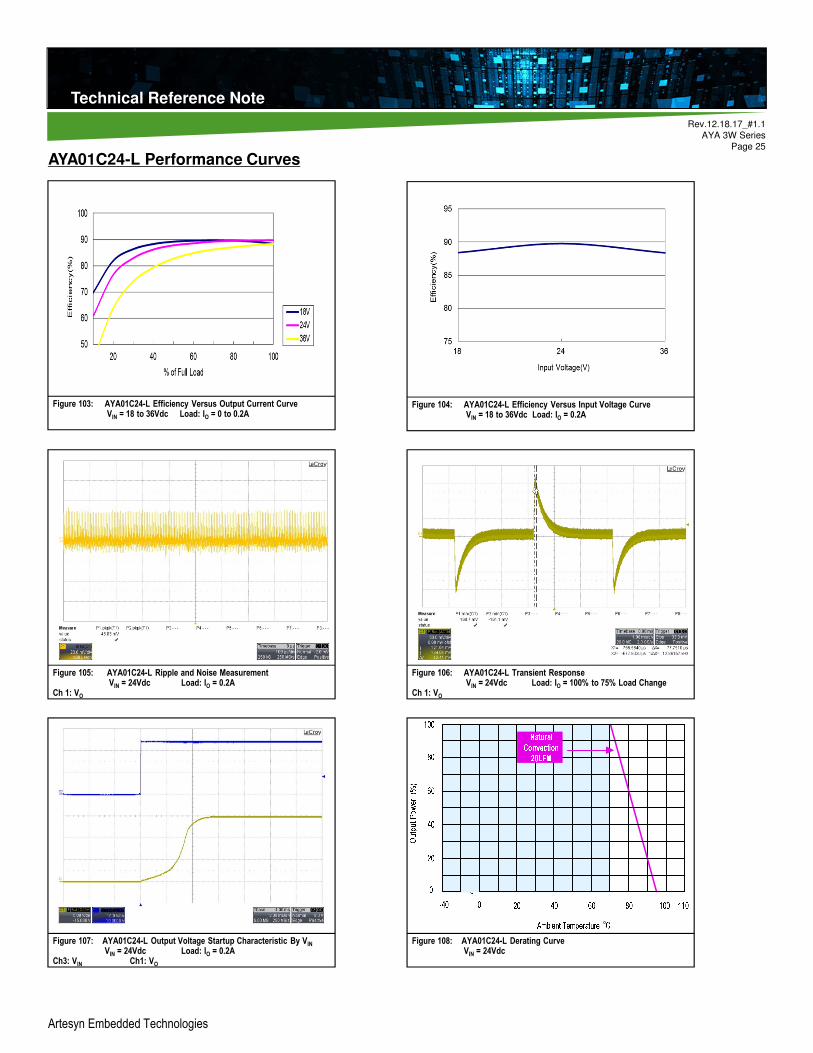
AYA01C24-L Performance Curves
Figure 106: AYA01C24-L Transient ResponseVIN = 24Vdc Load: IO = 100% to 75% Load Change
Ch 1: VO
Figure 103: AYA01C24-L Efficiency Versus Output Current CurveVIN = 18 to 36Vdc Load: IO = 0 to 0.2A
Figure 104: AYA01C24-L Efficiency Versus Input Voltage CurveVIN = 18 to 36Vdc Load: IO = 0.2A
Figure 105: AYA01C24-L Ripple and Noise MeasurementVIN = 24Vdc Load: IO = 0.2A
Ch 1: VO
Figure 107: AYA01C24-L Output Voltage Startup Characteristic By VIN
VIN = 24Vdc Load: IO = 0.2ACh3: VIN Ch1: VO
Figure 108: AYA01C24-L Derating CurveVIN = 24Vdc

Technical Reference Note
Rev.12.18.17_#1.1
AYA 3W Series
Page 26
Technical Reference Note
Artesyn Embedded Technologies
AYA01AA24-L Performance Curves
Figure 112: AYA01AA24-L Transient ResponseVIN = 24Vdc Load: IO = 100% to 75% Load Change
Ch 1: VO1 Ch2: VO2
Figure 109: AYA01AA24-L Efficiency Versus Output Current CurveVIN = 18 to 36Vdc Load: IO = ±±±±0.3A
Figure 110: AYA01AA24-L Efficiency Versus Input Voltage CurveVIN = 18 to 36Vdc Load: IO = ±±±±0.3A
Figure 111: AYA01AA24-L Ripple and Noise MeasurementVIN = 24Vdc Load: IO = ±±±±0.3A
Ch 1: VO1 Ch2: VO2
Figure 113: AYA01AA24-L Output Voltage Startup Characteristic By VIN
VIN = 24Vdc Load: IO = ±±±±0.3ACh3: VIN Ch1: VO1 Ch2: VO2
Figure 114: AYA01AA24-L Derating CurveVIN = 24Vdc
Technical Reference Note
Rev.12.18.17_#1.1
AYA 3W Series
Page 27
Technical Reference Note
Artesyn Embedded Technologies
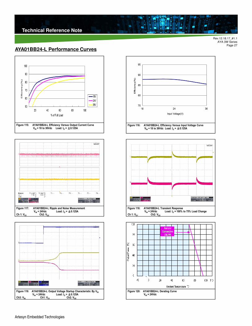
AYA01BB24-L Performance Curves
Figure 118: AYA01BB24-L Transient ResponseVIN = 24Vdc Load: IO = 100% to 75% Load Change
Ch 1: VO1 Ch2: VO2
Figure 115: AYA01BB24-L Efficiency Versus Output Current CurveVIN = 18 to 36Vdc Load: IO = ±±±±0.125A
Figure 116: AYA01BB24-L Efficiency Versus Input Voltage CurveVIN = 18 to 36Vdc Load: IO = ±±±±0.125A
Figure 117: AYA01BB24-L Ripple and Noise MeasurementVIN = 24Vdc Load: IO = ±±±±0.125A
Ch 1: VO1 Ch2: VO2
Figure 119: AYA01BB24-L Output Voltage Startup Characteristic By VIN
VIN = 24Vdc Load: IO = ±±±±0.125ACh3: VIN Ch1: VO1 Ch2: VO2
Figure 120: AYA01BB24-L Derating CurveVIN = 24Vdc

Technical Reference Note
Rev.12.18.17_#1.1
AYA 3W Series
Page 28
Technical Reference Note
Artesyn Embedded Technologies
AYA01CC24-L Performance Curves
Figure 124: AYA01CC24-L Transient ResponseVIN = 24Vdc Load: IO = 100% to 75% Load Change
Ch 1: VO1 Ch2: VO2
Figure 121: AYA01CC24-L Efficiency Versus Output Current CurveVIN = 18 to 36Vdc Load: IO = ±±±±0.1A
Figure 122: AYA01CC24-L Efficiency Versus Input Voltage CurveVIN = 18 to 36Vdc Load: IO = ±±±±0.1A
Figure 123: AYA01CC24-L Ripple and Noise MeasurementVIN = 24Vdc Load: IO = ±±±±0.1A
Ch 1: VO1 Ch2: VO2
Figure 125: AYA01CC24-L Output Voltage Startup Characteristic By VIN
VIN = 24Vdc Load: IO = ±±±±0.1ACh3: VIN Ch1: VO1 Ch2: VO2
Figure 126: AYA01CC24-L Derating CurveVIN = 24Vdc
Technical Reference Note
Rev.12.18.17_#1.1
AYA 3W Series
Page 29
Technical Reference Note
Artesyn Embedded Technologies
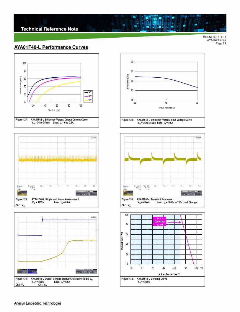
AYA01F48-L Performance Curves
Figure 130: AYA01F48-L Transient ResponseVIN = 48Vdc Load: IO = 100% to 75% Load Change
Ch 1: VO
Figure 127: AYA01F48-L Efficiency Versus Output Current CurveVIN = 36 to 75Vdc Load: IO = 0 to 0.6A
Figure 128: AYA01F48-L Efficiency Versus Input Voltage CurveVIN = 36 to 75Vdc Load: IO = 0.6A
Figure 129: AYA01F48-L Ripple and Noise MeasurementVIN = 48Vdc Load: IO = 0.6A
Ch 1: VO
Figure 131: AYA01F48-L Output Voltage Startup Characteristic By VIN
VIN = 48Vdc Load: IO = 0.6ACh3: VIN Ch1: VO
Figure 132: AYA01F48-L Derating CurveVIN = 48Vdc
Technical Reference Note
Rev.12.18.17_#1.1
AYA 3W Series
Page 30
Technical Reference Note
Artesyn Embedded Technologies
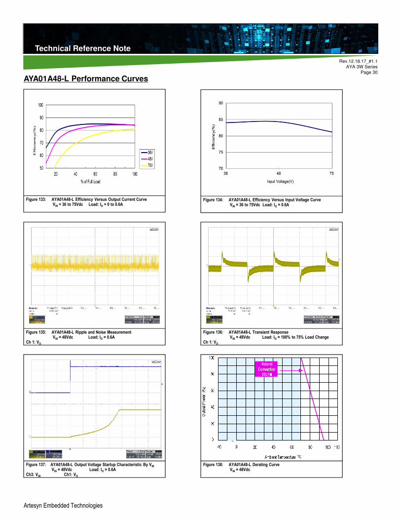
AYA01A48-L Performance Curves
Figure 136: AYA01A48-L Transient ResponseVIN = 48Vdc Load: IO = 100% to 75% Load Change
Ch 1: VO
Figure 133: AYA01A48-L Efficiency Versus Output Current CurveVIN = 36 to 75Vdc Load: IO = 0 to 0.6A
Figure 134: AYA01A48-L Efficiency Versus Input Voltage CurveVIN = 36 to 75Vdc Load: IO = 0.6A
Figure 135: AYA01A48-L Ripple and Noise MeasurementVIN = 48Vdc Load: IO = 0.6A
Ch 1: VO
Figure 137: AYA01A48-L Output Voltage Startup Characteristic By VIN
VIN = 48Vdc Load: IO = 0.6ACh3: VIN Ch1: VO
Figure 138: AYA01A48-L Derating CurveVIN = 48Vdc
Technical Reference Note
Rev.12.18.17_#1.1
AYA 3W Series
Page 31
Technical Reference Note
Artesyn Embedded Technologies
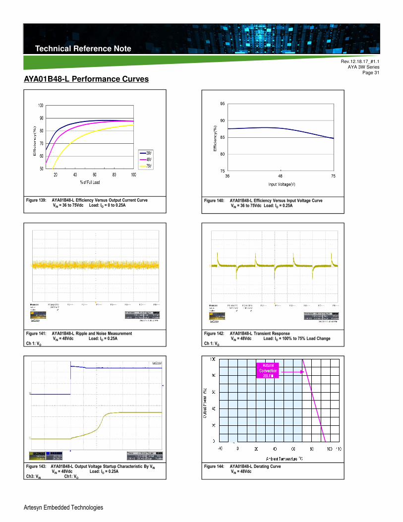
AYA01B48-L Performance Curves
Figure 142: AYA01B48-L Transient ResponseVIN = 48Vdc Load: IO = 100% to 75% Load Change
Ch 1: VO
Figure 139: AYA01B48-L Efficiency Versus Output Current CurveVIN = 36 to 75Vdc Load: IO = 0 to 0.25A
Figure 140: AYA01B48-L Efficiency Versus Input Voltage CurveVIN = 36 to 75Vdc Load: IO = 0.25A
Figure 141: AYA01B48-L Ripple and Noise MeasurementVIN = 48Vdc Load: IO = 0.25A
Ch 1: VO
Figure 143: AYA01B48-L Output Voltage Startup Characteristic By VIN
VIN = 48Vdc Load: IO = 0.25ACh3: VIN Ch1: VO
Figure 144: AYA01B48-L Derating CurveVIN = 48Vdc
Technical Reference Note
Rev.12.18.17_#1.1
AYA 3W Series
Page 32
Technical Reference Note
Artesyn Embedded Technologies
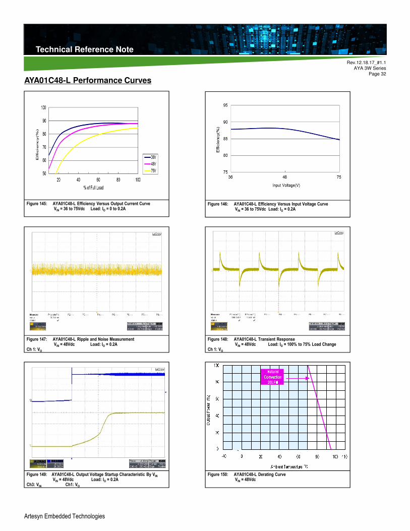
AYA01C48-L Performance Curves
Figure 148: AYA01C48-L Transient ResponseVIN = 48Vdc Load: IO = 100% to 75% Load Change
Ch 1: VO
Figure 145: AYA01C48-L Efficiency Versus Output Current CurveVIN = 36 to 75Vdc Load: IO = 0 to 0.2A
Figure 146: AYA01C48-L Efficiency Versus Input Voltage CurveVIN = 36 to 75Vdc Load: IO = 0.2A
Figure 147: AYA01C48-L Ripple and Noise MeasurementVIN = 48Vdc Load: IO = 0.2A
Ch 1: VO
Figure 149: AYA01C48-L Output Voltage Startup Characteristic By VIN
VIN = 48Vdc Load: IO = 0.2ACh3: VIN Ch1: VO
Figure 150: AYA01C48-L Derating CurveVIN = 48Vdc

Technical Reference Note
Rev.12.18.17_#1.1
AYA 3W Series
Page 33
Technical Reference Note
Artesyn Embedded Technologies
AYA01AA48-L Performance Curves
Figure 154: AYA01AA48-L Transient ResponseVIN = 48Vdc Load: IO = 100% to 75% Load Change
Ch1: VO1 Ch 2: VO2
Figure 151: AYA01AA48-L Efficiency Versus Output Current CurveVIN = 36 to 75Vdc Load: IO = 0 to ±±±± 0.3A
Figure 152: AYA01AA48-L Efficiency Versus Input Voltage CurveVIN = 36 to 75Vdc Load: IO = ±±±± 0.3A
Figure 153: AYA01AA48-L Ripple and Noise MeasurementVIN = 48Vdc Load: IO = ±±±± 0.3A
Ch1: VO1 Ch 2: VO2
Figure 155: AYA01AA48-L Output Voltage Startup Characteristic By VIN
VIN = 48Vdc Load: IO = ±±±± 0.3ACh3: VIN Ch1: VO1 Ch2: VO2
Figure 156: AYA01AA48-L Derating CurveVIN = 48Vdc

Technical Reference Note
Rev.12.18.17_#1.1
AYA 3W Series
Page 34
Technical Reference Note
Artesyn Embedded Technologies
AYA01BB48-L Performance Curves
Figure 160: AYA01BB48-L Transient ResponseVIN = 48Vdc Load: IO = 100% to 75% Load Change
Ch1: VO1 Ch 2: VO2
Figure 157: AYA01BB48-L Efficiency Versus Output Current CurveVIN = 36 to 75Vdc Load: IO = 0 to ±±±± 0.125A
Figure 158: AYA01BB48-L Efficiency Versus Input Voltage CurveVIN = 36 to 75Vdc Load: IO = ±±±± 0.125A
Figure 159: AYA01BB48-L Ripple and Noise MeasurementVIN = 48Vdc Load: IO = ±±±± 0.125A
Ch1: VO1 Ch 2: VO2
Figure 161: AYA01BB48-L Output Voltage Startup Characteristic By VIN
VIN = 48Vdc Load: IO = ±±±± 0.125ACh3: VIN Ch1: VO1 Ch2: VO2
Figure 162: AYA01BB48-L Derating CurveVIN = 48Vdc
Technical Reference Note
Rev.12.18.17_#1.1
AYA 3W Series
Page 35
Technical Reference Note
Artesyn Embedded Technologies
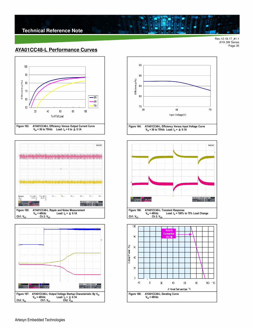
AYA01CC48-L Performance Curves
Figure 166: AYA01CC48-L Transient ResponseVIN = 48Vdc Load: IO = 100% to 75% Load Change
Ch1: VO1 Ch 2: VO2
Figure 163: AYA01CC48-L Efficiency Versus Output Current CurveVIN = 36 to 75Vdc Load: IO = 0 to ±±±± 0.1A
Figure 164: AYA01CC48-L Efficiency Versus Input Voltage CurveVIN = 36 to 75Vdc Load: IO = ±±±± 0.1A
Figure 165: AYA01CC48-L Ripple and Noise MeasurementVIN = 48Vdc Load: IO = ±±±± 0.1A
Ch1: VO1 Ch 2: VO2
Figure 167: AYA01CC48-L Output Voltage Startup Characteristic By VIN
VIN = 48Vdc Load: IO = ±±±± 0.1ACh3: VIN Ch1: VO1 Ch2: VO2
Figure 168: AYA01CC48-L Derating CurveVIN = 48Vdc
Technical Reference Note
Rev.12.18.17_#1.1
AYA 3W Series
Page 36
Technical Reference Note
Artesyn Embedded Technologies
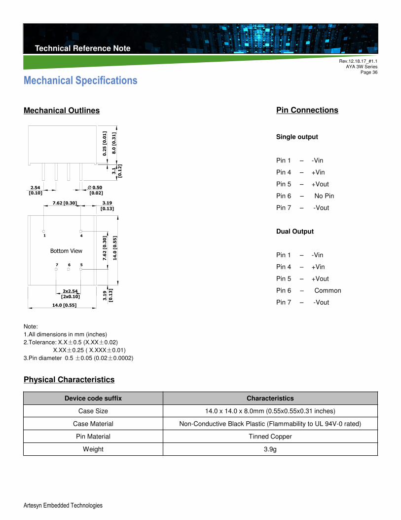
Mechanical Specifications
Mechanical Outlines
Note:
1.All dimensions in mm (inches)
2.Tolerance: X.X±0.5 (X.XX±0.02)
X.XX±0.25 ( X.XXX±0.01)
3.Pin diameter 0.5±0.05 (0.02±0.0002)
Physical Characteristics
Pin Connections
Single output
Pin 1 – -Vin
Pin 4 – +Vin
Pin 5 – +Vout
Pin 6 – No Pin
Pin 7 – -Vout
Dual Output
Pin 1 – -Vin
Pin 4 – +Vin
Pin 5 – +Vout
Pin 6 – Common
Pin 7 – -Vout
Device code suffix Characteristics
Case Size 14.0 x 14.0 x 8.0mm (0.55x0.55x0.31 inches)
Case Material Non-Conductive Black Plastic (Flammability to UL 94V-0 rated)
Pin Material Tinned Copper
Weight 3.9g
1 4
7 5
Bottom View
3.1
[0.1
2]
0.2
5 [
0.0
1]
2x2.54
[2x0.10]
2.54
[0.10]
3.19
[0.13]
7.6
2 [
0.3
0]
14
.0 [
0.5
5]
3.1
9
[0.1
3]
14.0 [0.55]
7.62 [0.30]
0.50
[0.02]
8.0
[0
.31
]
6
Technical Reference Note
Rev.12.18.17_#1.1
AYA 3W Series
Page 37
Technical Reference Note
Artesyn Embedded Technologies
Recommended Pad Layout for Single & Dual Output Converter
TOP View
5
1
KEEP OUT AREA
67
4
5x 2.1±0.04
( 0.082±0.1)(PAD)
5x 0.9
( 0.035 )(HOLE)
+0.01
- 0+0.01
- 0
14.00 [0.55]
2.54
[0.10]
2.54
[0.10]
7.6
2 [
0.3
0]
3.1
9
[0.1
3]
14.0
0 [
0.5
5]
7.62 [0.30] 3.19[0.13]
Note:
All dimensions in mm (inches)
Technical Reference Note
Rev.12.18.17_#1.1
AYA 3W Series
Page 38
Technical Reference Note
Artesyn Embedded Technologies
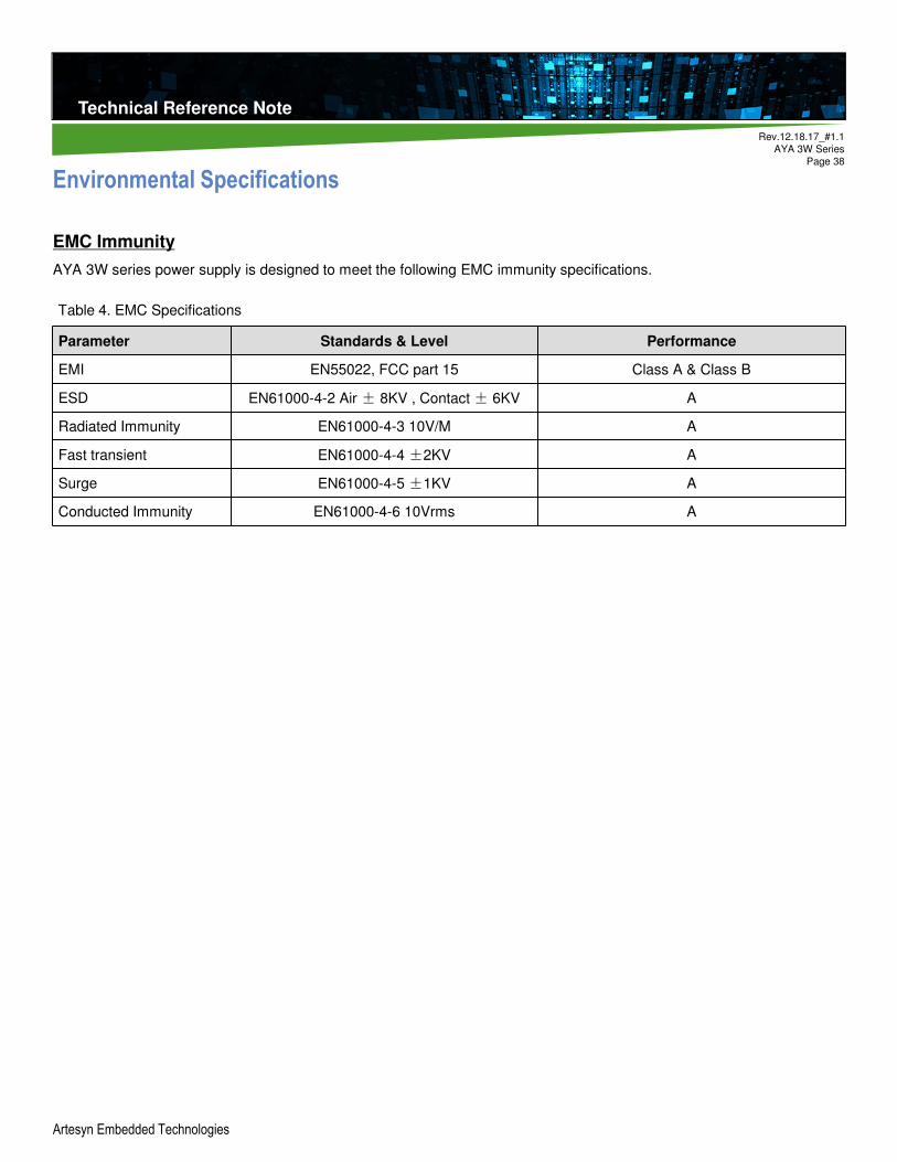
Environmental Specifications
EMC Immunity
AYA 3W series power supply is designed to meet the following EMC immunity specifications.
Table 4. EMC Specifications
Parameter Standards & Level Performance
EMI EN55022, FCC part 15 Class A & Class B
ESD EN61000-4-2 Air ± 8KV , Contact ± 6KV A
Radiated Immunity EN61000-4-3 10V/M A
Fast transient EN61000-4-4 ±2KV A
Surge EN61000-4-5 ±1KV A
Conducted Immunity EN61000-4-6 10Vrms A
Technical Reference Note
Rev.12.18.17_#1.1
AYA 3W Series
Page 39
Technical Reference Note
Artesyn Embedded Technologies
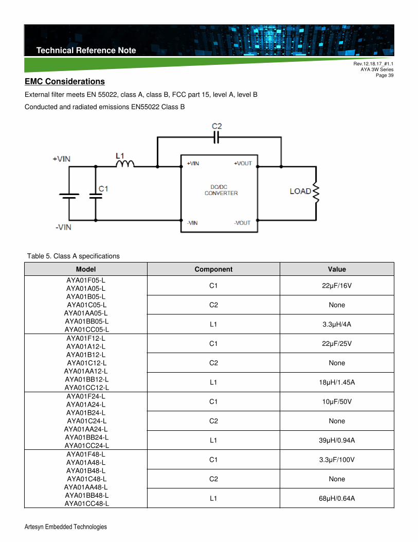
EMC Considerations
External filter meets EN 55022, class A, class B, FCC part 15, level A, level B
Conducted and radiated emissions EN55022 Class B
Table 5. Class A specifications
Model Component Value
AYA01F05-L
AYA01A05-L
AYA01B05-L
AYA01C05-L
AYA01AA05-L
AYA01BB05-L
AYA01CC05-L
C1 22μF/16V
C2 None
L1 3.3μH/4A
AYA01F12-L
AYA01A12-L
AYA01B12-L
AYA01C12-L
AYA01AA12-L
AYA01BB12-L
AYA01CC12-L
C1 22μF/25V
C2 None
L1 18μH/1.45A
AYA01F24-L
AYA01A24-L
AYA01B24-L
AYA01C24-L
AYA01AA24-L
AYA01BB24-L
AYA01CC24-L
C1 10μF/50V
C2 None
L1 39μH/0.94A
AYA01F48-L
AYA01A48-L
AYA01B48-L
AYA01C48-L
AYA01AA48-L
AYA01BB48-L
AYA01CC48-L
C1 3.3μF/100V
C2 None
L1 68μH/0.64A
Technical Reference Note
Rev.12.18.17_#1.1
AYA 3W Series
Page 40
Technical Reference Note
Artesyn Embedded Technologies
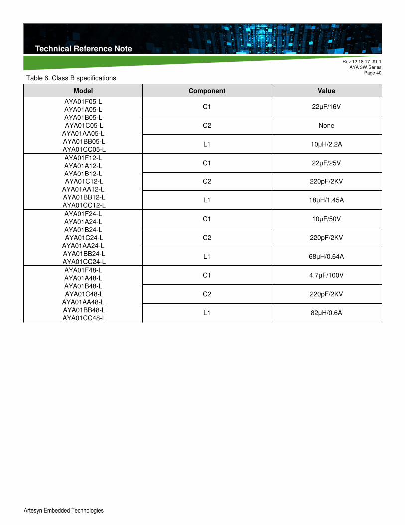
Table 6. Class B specifications
Model Component Value
AYA01F05-L
AYA01A05-L
AYA01B05-L
AYA01C05-L
AYA01AA05-L
AYA01BB05-L
AYA01CC05-L
C1 22μF/16V
C2 None
L1 10μH/2.2A
AYA01F12-L
AYA01A12-L
AYA01B12-L
AYA01C12-L
AYA01AA12-L
AYA01BB12-L
AYA01CC12-L
C1 22μF/25V
C2 220pF/2KV
L1 18μH/1.45A
AYA01F24-L
AYA01A24-L
AYA01B24-L
AYA01C24-L
AYA01AA24-L
AYA01BB24-L
AYA01CC24-L
C1 10μF/50V
C2 220pF/2KV
L1 68μH/0.64A
AYA01F48-L
AYA01A48-L
AYA01B48-L
AYA01C48-L
AYA01AA48-L
AYA01BB48-L
AYA01CC48-L
C1 4.7μF/100V
C2 220pF/2KV
L1 82μH/0.6A
Technical Reference Note
Rev.12.18.17_#1.1
AYA 3W Series
Page 41
Technical Reference Note
Artesyn Embedded Technologies
Safety Certifications
The AYA 3W power supply is intended for inclusion in other equipment and the installer must ensure that it is in
compliance with all the requirements of the end application. This product is only for inclusion by professional installers
within other equipment and must not be operated as a stand alone product.
Table 4. Safety Certifications for AYA series power supply system
Document Description
cUL/UL 60950-1 (UL certificate) US and Canada Requirements
IEC/EN 60950-1 (CB-scheme) European Requirements
Technical Reference Note
Rev.12.18.17_#1.1
AYA 3W Series
Page 42
Technical Reference Note
Artesyn Embedded Technologies
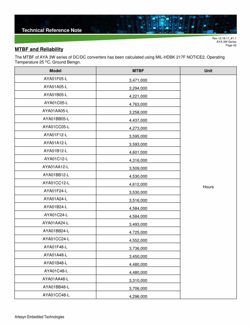
MTBF and Reliability
The MTBF of AYA 3W series of DC/DC converters has been calculated using MIL-HDBK 217F NOTICE2, Operating
Temperature 25 OC, Ground Benign.
Model MTBF Unit
AYA01F05-L 3,471,000
Hours
AYA01A05-L 3,294,000
AYA01B05-L 4,221,000
AYA01C05-L 4,763,000
AYA01AA05-L 3,258,000
AYA01BB05-L 4,437,000
AYA01CC05-L 4,273,000
AYA01F12-L 3,595,000
AYA01A12-L 3,593,000
AYA01B12-L 4,601,000
AYA01C12-L 4,316,000
AYA01AA12-L 3,509,000
AYA01BB12-L 4,530,000
AYA01CC12-L 4,612,000
AYA01F24-L 3,530,000
AYA01A24-L 3,516,000
AYA01B24-L 4,584,000
AYA01C24-L 4,584,000
AYA01AA24-L 3,493,000
AYA01BB24-L 4,725,000
AYA01CC24-L 4,552,000
AYA01F48-L 3,736,000
AYA01A48-L 3,450,000
AYA01B48-L 4,480,000
AYA01C48-L 4,480,000
AYA01AA48-L 3,310,000
AYA01BB48-L 3,706,000
AYA01CC48-L 4,296,000
Technical Reference Note
Rev.12.18.17_#1.1
AYA 3W Series
Page 43
Technical Reference Note
Artesyn Embedded Technologies
Application Notes
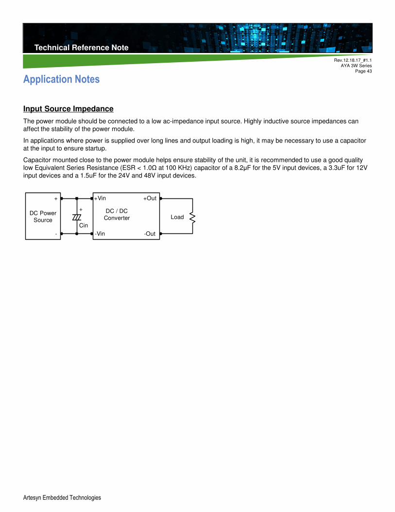
Input Source Impedance
The power module should be connected to a low ac-impedance input source. Highly inductive source impedances can
affect the stability of the power module.
In applications where power is supplied over long lines and output loading is high, it may be necessary to use a capacitor
at the input to ensure startup.
Capacitor mounted close to the power module helps ensure stability of the unit, it is recommended to use a good quality
low Equivalent Series Resistance (ESR < 1.0Ω at 100 KHz) capacitor of a 8.2μF for the 5V input devices, a 3.3uF for 12V
input devices and a 1.5uF for the 24V and 48V input devices.
+
+Out
-Out
+Vin
-Vin
DC / DCConverter Load
DC PowerSource
+
-
Cin
Technical Reference Note
Rev.12.18.17_#1.1
AYA 3W Series
Page 44
Technical Reference Note
Artesyn Embedded Technologies
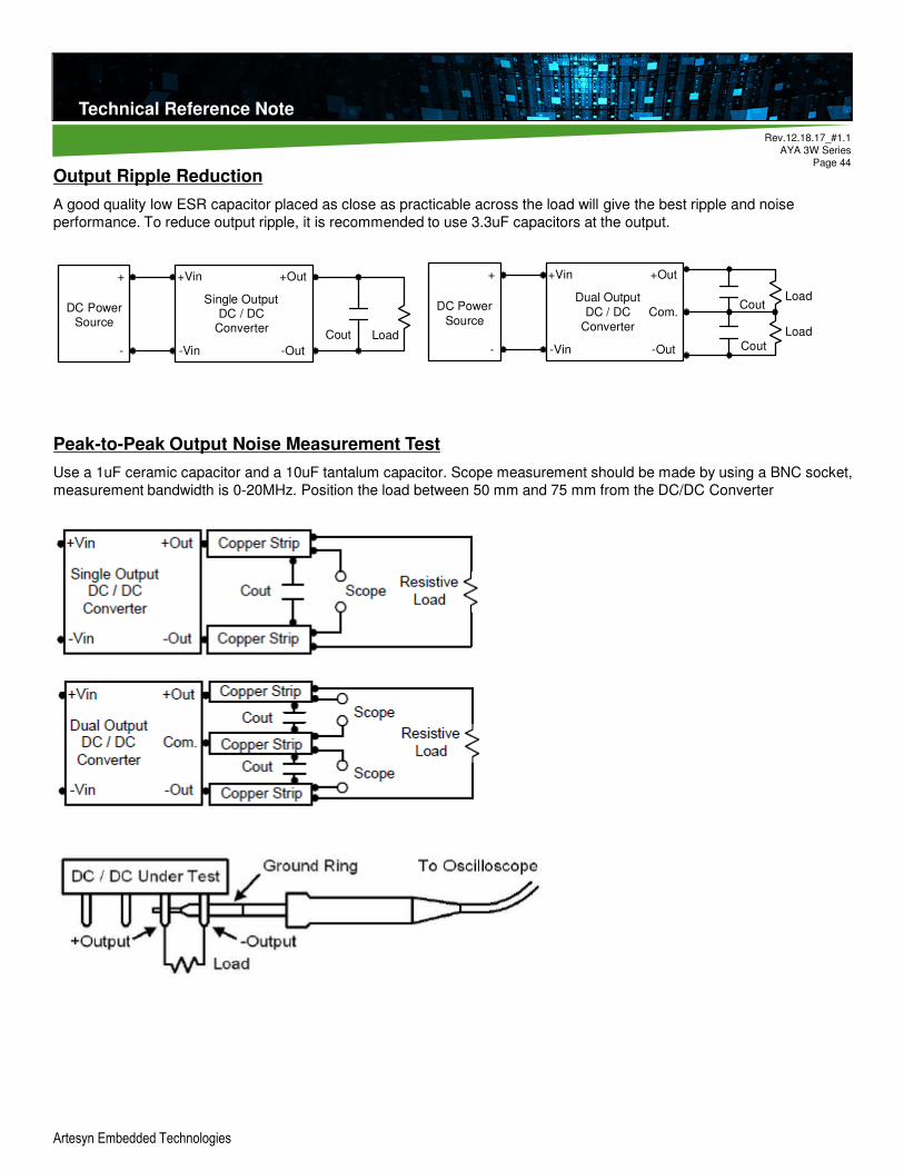
Output Ripple Reduction
A good quality low ESR capacitor placed as close as practicable across the load will give the best ripple and noise
performance. To reduce output ripple, it is recommended to use 3.3uF capacitors at the output.
Peak-to-Peak Output Noise Measurement Test
Use a 1uF ceramic capacitor and a 10uF tantalum capacitor. Scope measurement should be made by using a BNC socket,
measurement bandwidth is 0-20MHz. Position the load between 50 mm and 75 mm from the DC/DC Converter
+Out
-Out
+Vin
-Vin
Load
DC PowerSource
+
-
Cout
Single OutputDC / DC
Converter
+Out
-Out
+Vin
-Vin
LoadDC Power
Source
+
-
CoutCom.
Dual Output
DC / DC
Converter LoadCout
Technical Reference Note
Rev.12.18.17_#1.1
AYA 3W Series
Page 45
Technical Reference Note
Artesyn Embedded Technologies
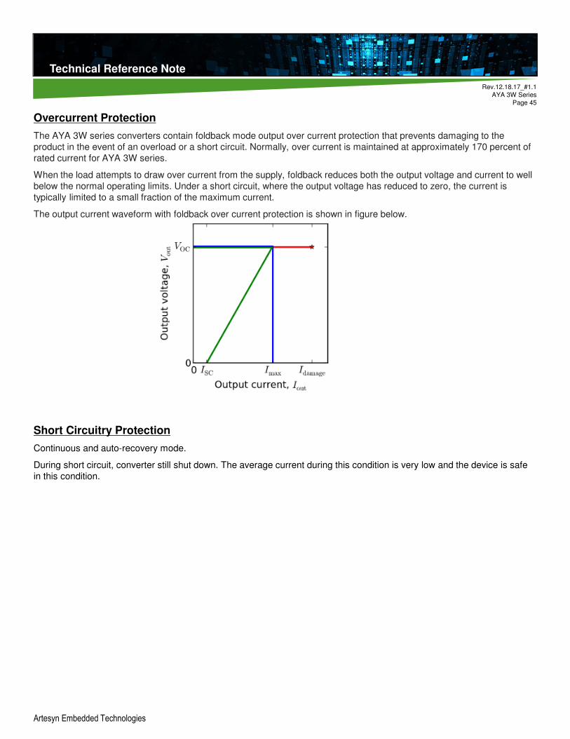
Overcurrent Protection
The AYA 3W series converters contain foldback mode output over current protection that prevents damaging to the
product in the event of an overload or a short circuit. Normally, over current is maintained at approximately 170 percent of
rated current for AYA 3W series.
When the load attempts to draw over current from the supply, foldback reduces both the output voltage and current to well
below the normal operating limits. Under a short circuit, where the output voltage has reduced to zero, the current is
typically limited to a small fraction of the maximum current.
The output current waveform with foldback over current protection is shown in figure below.
Short Circuitry Protection
Continuous and auto-recovery mode.
During short circuit, converter still shut down. The average current during this condition is very low and the device is safe
in this condition.
Technical Reference Note
Rev.12.18.17_#1.1
AYA 3W Series
Page 46
Technical Reference Note
Artesyn Embedded Technologies
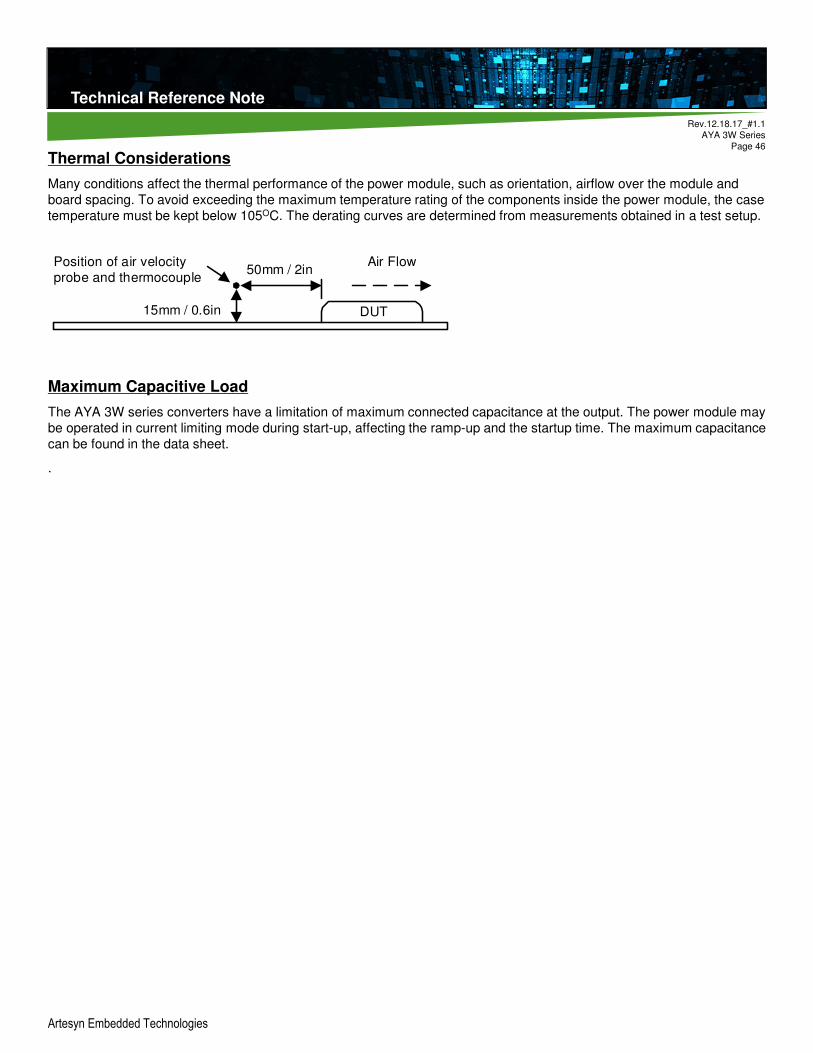
Thermal Considerations
Many conditions affect the thermal performance of the power module, such as orientation, airflow over the module and
board spacing. To avoid exceeding the maximum temperature rating of the components inside the power module, the case
temperature must be kept below 105OC. The derating curves are determined from measurements obtained in a test setup.
Maximum Capacitive Load
The AYA 3W series converters have a limitation of maximum connected capacitance at the output. The power module may
be operated in current limiting mode during start-up, affecting the ramp-up and the startup time. The maximum capacitance
can be found in the data sheet.
.
DUT
Position of air velocityprobe and thermocouple
50mm / 2inAir Flow
15mm / 0.6in
Technical Reference Note
Rev.12.18.17_#1.1
AYA 3W Series
Page 47
Technical Reference Note
Artesyn Embedded Technologies
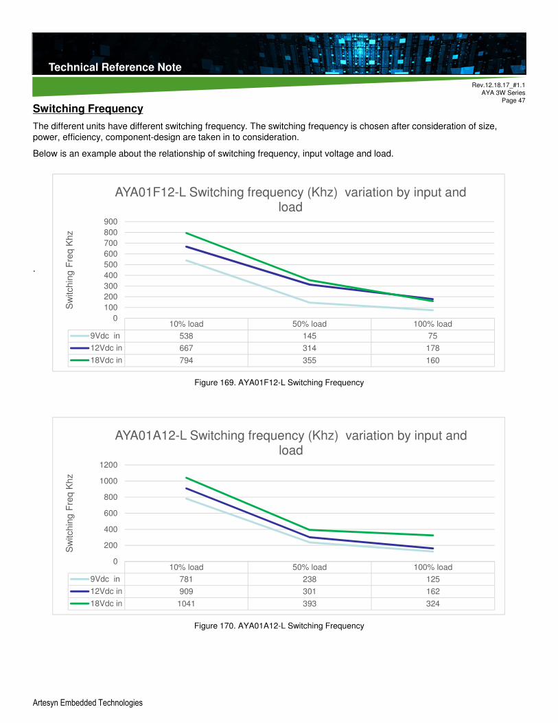
Switching Frequency
The different units have different switching frequency. The switching frequency is chosen after consideration of size,
power, efficiency, component-design are taken in to consideration.
Below is an example about the relationship of switching frequency, input voltage and load.
.
Figure 169. AYA01F12-L Switching Frequency
Figure 170. AYA01A12-L Switching Frequency
10% load 50% load 100% load
9Vdc in 538 145 75
12Vdc in 667 314 178
18Vdc in 794 355 160
0
100
200
300
400
500
600
700
800
900
Sw
itchin
g F
req K
hz
AYA01F12-L Switching frequency (Khz) variation by input and load
10% load 50% load 100% load
9Vdc in 781 238 125
12Vdc in 909 301 162
18Vdc in 1041 393 324
0
200
400
600
800
1000
1200
Sw
itchin
g F
req K
hz
AYA01A12-L Switching frequency (Khz) variation by input and load
Technical Reference Note
Rev.12.18.17_#1.1
AYA 3W Series
Page 48
Technical Reference Note
Artesyn Embedded Technologies
.
.
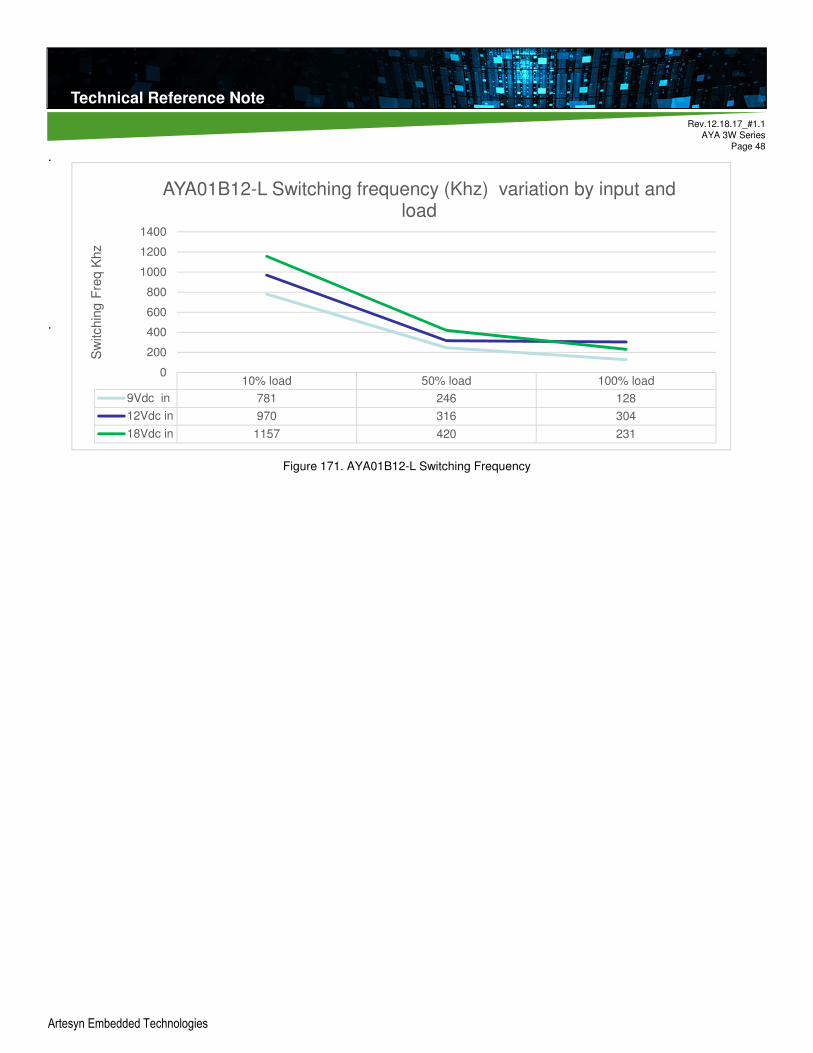
Figure 171. AYA01B12-L Switching Frequency
10% load 50% load 100% load
9Vdc in 781 246 128
12Vdc in 970 316 304
18Vdc in 1157 420 231
0
200
400
600
800
1000
1200
1400
Sw
itchin
g F
req K
hz
AYA01B12-L Switching frequency (Khz) variation by input and load
Technical Reference Note
Rev.12.18.17_#1.1
AYA 3W Series
Page 49
Technical Reference Note
Artesyn Embedded Technologies
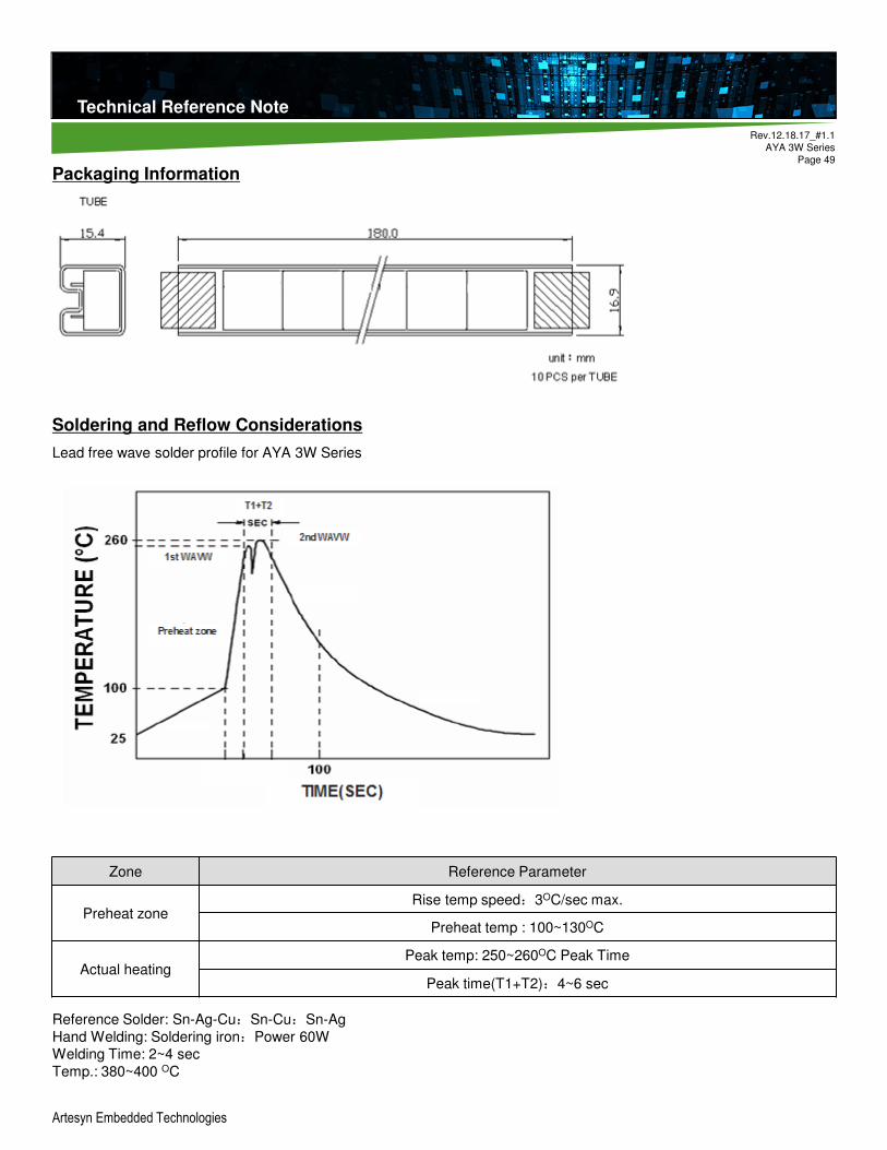
Packaging Information
Soldering and Reflow Considerations
Lead free wave solder profile for AYA 3W Series
Reference Solder: Sn-Ag-Cu:Sn-Cu:Sn-Ag
Hand Welding: Soldering iron:Power 60WWelding Time: 2~4 sec
Temp.: 380~400 OC
Zone Reference Parameter
Preheat zoneRise temp speed:3OC/sec max.
Preheat temp : 100~130OC
Actual heating Peak temp: 250~260OC Peak Time
Peak time(T1+T2):4~6 sec
Technical Reference Note
Rev.12.18.17_#1.1
AYA 3W Series
Page 50
Technical Reference Note
Artesyn Embedded Technologies
Weight
The typical weight of AYA 3W series converters is 3.9g.
Technical Reference Note
Rev.12.18.17_#1.1
AYA 3W Series
Page 51
Technical Reference Note
For more information: www.artesyn.com/power
For support: [email protected]
Record of Revision and Changes
Issue Date Description Originators
1.0 09.23.2016 First Issue Leo.L
1.1 12.18.2017 Update the Switching Frequency Leo.L


![J]3W~W - FlacsoAndes](https://img.pdfslide.tips/doc/110x75/61f37564c71357591c0885f1/j3ww-flacsoandes.jpg)