1
DOI: 10.1002/ ((please add manuscript number))
Article type: Full Paper
Tunable magnetism in nanoporous CuNi alloys by reversible voltage-driven element-
selective redox processes
Alberto Quintana,* Enric Menéndez,* Eloy Isarain-Chávez, Jordina Fornell, Pau Solsona,
François Fauth, Maria Dolors Baró, Josep Nogués, Eva Pellicer, Jordi Sort*
Alberto Quintana, Dr. Enric Menéndez, Dr. Eloy Isarain-Chávez, Dr. Jordina Fornell, Dr. Pau
Solsona, Prof. Maria Dolors Baró, Dr. Eva Pellicer and Prof. Jordi Sort
Departament de Física, Universitat Autònoma de Barcelona, E-08193 Cerdanyola del Vallès,
Spain
[email protected], [email protected], [email protected]
Dr. François Fauth
CELLS-ALBA, BP1413, 08290 Cerdanyola del Vallès, Spain
Prof. Josep Nogués
Catalan Institute of Nanoscience and Nanotechnology (ICN2), CSIC and The Barcelona
Institute of Science and Technology, Campus UAB, Cerdanyola del Vallès, E-08193
Barcelona, Spain
Prof. Jordi Sort and Prof. Josep Nogués
Institució Catalana de Recerca i Estudis Avançats (ICREA), Pg. Lluís Companys 23, E-08010
Barcelona, Spain
Keywords: magneto-electric effects, nanoporous alloys, redox processes
Voltage-driven manipulation of magnetism in electrodeposited 200 nm-thick nanoporous
single-phase solid solution Cu20Ni80 (at. %) alloy films (with sub-10 nm pore size) is
accomplished by controlled reduction-oxidation (i.e., redox) processes in a protic solvent,
namely 1M NaOH aqueous solution. Owing to the selectivity of the electrochemical
processes, the oxidation of the CuNi film mainly occurs on the Cu counterpart of the solid
solution, resulting in a Ni-enriched alloy. As a consequence, the magnetic moment at
saturation significantly increases (up to 33 % enhancement with respect to the as-prepared
sample), while only slight changes in coercivity are observed. Conversely, the reduction
process brings Cu back to its metallic state and, remarkably, it becomes alloyed to Ni again.

2
The reported phenomenon is fully reversible, thus allowing for the precise adjustment of the
magnetic properties of this system through the sign and amplitude of the applied voltage.
1. Introduction
Since the pioneering studies on magnetoelectric effects in the 50’s and 60’s, a flurry of
research has been undertaken on the electric control of magnetism.[1]
Conventional
magnetoelectric studies focused on strain-mediated systems, in which the magnetic properties
were modified by the interfacial coupling between piezoelectric and magnetostrictive
counterparts.[2]
However, the strain caused by the voltage in these heterostructured systems
limits the applications of this phenomenon in technological devices due to fatigue-induced
mechanical failure. Controlling magnetism with electric fields without involving strain is an
emerging field of research and might boost current magnetic technologies. Novel applications
such as low power or multilevel voltage-controlled magnetic memories are envisaged.[3]
Due to the intrinsic coupling between ferroic orders, single-phase multiferroics are the most
promising candidates for magnetoelectric applications not mediated by strain. However, so
far, the observed magnetoelectric coupling is weak, thus hindering its use in real devices.[4]
Moreover, the amount of intrinsic multiferroic materials is rather limited since the underlying
physical mechanisms of ferroelectricity and magnetism are different and tend to exclude each
other.[5]
To overcome these drawbacks, several approaches to electrically tailor magnetism are
being proposed. For example, another route consists in the injection of electrostatic charges to
a ferromagnetic material in order to modify its electronic band structure and, consequently, its
magnetic anisotropy and magnetization.[6]
This is commonly accomplished by preparing a
condenser-like configuration in which a dielectric material is sandwiched between the
ferromagnetic material of interest and a metallic electrode. Materials with a high dielectric

3
constant are preferred, with the aim of being able to accumulate large amounts of electrostatic
charges. However, some of these dielectrics also exhibit high ion mobility, e.g., HfO2 or
Gd2O3. In this case, oxygen diffusion (and the concomitant oxidation-reduction processes)
may play a predominant role, even overcoming charge accumulation effects during voltage
actuation and, thus, becoming the main factor determining the overall magnetic properties of
the system. Similar phenomena have been reported in ferromagnetic/ferroelectric interfaces
prior and after voltage application.[7]
Actually, controlled plasma oxygen has been utilized to
externally promote oxygen migration and tailor perpendicular magnetic anisotropy in
Pt/Co/AlOx systems via Co-O hybridization at the interface between Co and Al.[8]
A
reversible change of the perpendicular magnetic anisotropy by voltage actuation has been
reported in Pt/Co/GdOx layers due to the diffusion of O2-
from the oxide to the cobalt layer.[9]
The voltage control of oxygen migration (i.e., controlled oxidation and reduction) with the
aim of modifying magnetism in both solid state[9,10]
and liquid[11]
ferromagnetic/insulating
interfaces has evidenced very satisfactory results and has led to the emergence of magneto-
ionics as a means to induce magnetoelectric effects.
In general, when a material is subjected to an electric field, charge accumulation, redox
processes and magnetostriction (the latter only in case piezoelectric materials are involved)
may simultaneously occur. Disentangling these contributions is essential to further control
magnetism by voltage actuation. All these phenomena are interface-driven and, consequently,
are expected to be maximized in materials with a high surface area-to-volume ratio. Although
this is typically achieved in ultrathin films, nanoporous magnetic alloys, with extremely large
surface area-to-volume ratios, may be an appealing alternative.[12]
However, so far,
magnetoelectric effects in nanoporous materials have been rather overlooked.
In a previous study, we showed that the coercivity of CuNi nanoporous alloys can be
drastically reduced by voltage actuation using an organic aprotic (and water-free) electrolyte,

4
essentially due to purely electrically-induced changes in the magnetic anisotropy. This effect
could be utilized to significantly reduce energy consumption in magnetically actuated devices.
In this article, we present a voltage-driven electrochemical approach to tailor not the
coercivity but the overall magnetization of ferromagnetic nanoporous Cu20Ni80 films using an
aqueous electrolyte (i.e., via controlled electrochemical redox processes). The strong element
selectivity of the oxidation process allows for an enhancement of the magnetic moment at
saturation up to 33%. This effect turns out to be fully reversible by changing the sign of the
applied voltage. Besides the interest of these results in the field of magnetic devices and
spintronics, our work also contributes to extend the potential applications of porous materials,
so far mainly employed in fields such as catalysis,[13]
water cleaning,[14]
self-cleaning and
super-hydrophobic surfaces[15]
and energy storage and conversion.[16]
2. Results and discussion
Figure 1a shows a representative scanning electron microscopy (SEM) image of an as-
prepared nanoporous Cu20Ni80 film. A homogenous granular morphology is observed at the
surface of the film. The size of these granules typically ranges between 50 and 200 nm. A
magnified image (Figure 1b) reveals that these clusters are, in fact, nanoporous, i.e. they
consist of agglomerated sub-10 nm nanoparticles. The morphology along sample thickness
was characterized by scanning transmission electron microscopy (STEM) and transmission
electron microscopy (TEM) (Figure 1c and 1d, respectively). STEM reveals that the porosity
spans the whole thickness of the film, where the bottom bright layer in the STEM image
corresponds to the Au surface. The nanoporous morphology is further confirmed by high
resolution TEM (Figure 1d), from which the average pore size can be estimated to be between
5 and 7 nm. Compositional analyses performed by energy dispersive X-ray analyses (EDX)
give Cu and Ni contents of 20 and 80 at. %, respectively.

5
The as-prepared samples were characterized from a structural viewpoint by synchrotron
grazing incidence X-ray diffraction (GIXRD) at the ALBA light source facility. As can be
seen in Figure 2, the GIXRD pattern of an as-prepared sample exhibits several XRD peaks
arising from face centered cubic Cu20Ni80, indicating the polycrystalline nature of the film. No
additional peaks from pure Cu or Ni are observed, ruling out phase separation and, thus,
indicating that the Cu and Ni grow forming a solid solution.
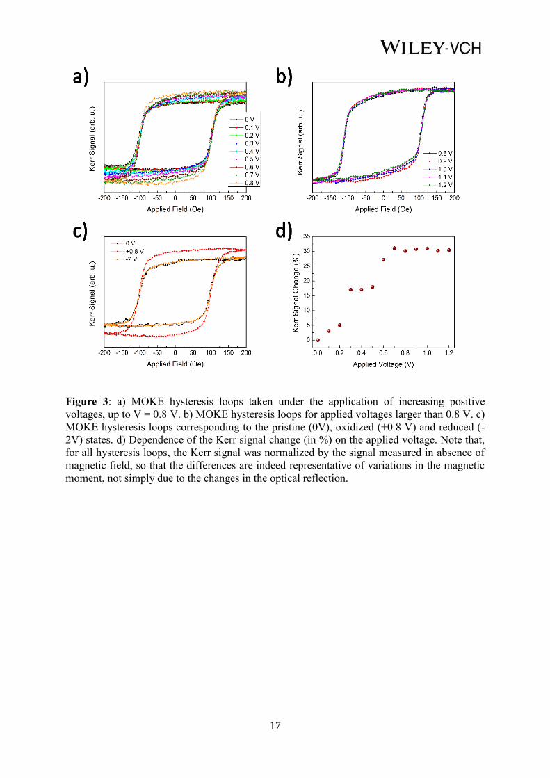
In order to investigate the voltage-driven redox processes, in-situ magneto-optic Kerr effect
measurements at selected oxidation/reduction voltages were carried out in liquid medium.
Prior to the first measurement (i.e., 0 V), the sample was submerged in the electrolyte during
30 minutes in order to allow the solution (1M NaOH) wet the nanopores by capillary action.
Subsequently, hysteresis loops were acquired at increasingly applied voltages in steps of 0.1
V, up to a maximum applied voltage V = +1.2 V. The as-prepared sample exhibits a rather
square-shaped loop with a coercivity around 100 Oe, indicating an in-plane easy axis. As can
be seen in Figure 3a, while the coercivity remains rather unaltered with the applied voltage
(relative changes are below 5 %), the magneto-optic Kerr effect (MOKE) signal (i.e., the
amplitude of the MOKE signal) monotonously increases with the applied voltage up to V = +
0.8 V. Figure 3b shows that no significant changes are observed beyond + 0.8 V, confirming
that the Kerr signal tends to saturate at + 0.8 V. Remarkably, the pristine magnetic state (i.e.,
same coercivity and Kerr signal) can be recovered by applying negative voltages. Full
recovery is achieved after applying –2 V for 10 min (Figure 3c). Since, in a first
approximation, the Kerr signal can be considered to be proportional to the magnetic
moment,[17]
the increase in Kerr signal with positive voltages can be understood as an increase
of the magnetic moment in the film volume probed by MOKE. This change in Kerr signal can
be quantified as follows (see scheme in Figure S1):
% change = ((Ak(V) - Ak(0)) / Ak(0)) x 100 (1)

6
where Ak(V) is the difference in Kerr signal between positive and negative saturation and
Ak(0) is the Kerr signal amplitude at 0V. Figure 3d represents the change in Kerr signal as a
function of the positive applied voltage. The maximum relative increase in the Kerr signal
amplitude is 33%, for an applied voltage V = + 0.8 V.
In order to elucidate if any structural change is responsible for the observed magneto-electric
effect, synchrotron XRD measurements were carried out ex-situ in grazing incidence (2° as
angle of incidence) mode for the as-prepared sample, after subjected to oxidation at +0.8 V
and the sample reduced using –2 V.
As can be seen in Figure 4, upon oxidation, the (220) Cu20Ni80 GIXRD peak significantly
shifts towards higher 2θ angles (0.2° difference), indicating a decrease of the lattice cell
parameter which could be ascribed to a change in composition in the Cu-Ni solid solution,
more specifically, to an increase in the Ni content.[18]
This is consistent with the obtained
magnetic results since an increase in the Ni content would explain the enhancement of Kerr
signal (i.e., magnetic moment) upon the application of positive voltages. Such an increase of
the Ni content would indicate that Cu preferentially oxidizes during the application of a
positive voltage.[19]
Negem and Nady studied the oxidation of nanocrystalline Cu-Ni alloys in
1.0 M KOH solution and found that the oxidation peaks recorded in cyclic voltammetry
studies were related to the formation of oxidized Cu species (Cu(OH)ads–
→ Cu2O →
Cu(OH)2). Parallel cyclic voltammetry studies with electrodeposited pure Ni counterpart
showed the absence of oxidation peaks in the anodic scan.[20]
Interestingly, when negative
voltages are applied, the (220) Cu-Ni GIXRD peak shifts back to the initial position,
suggesting that the positive voltage not only induces reduction of the previously oxidized
atoms but also the metallic Cu reincorporates into the Cu-Ni solid solution. In other words,
the original composition (Cu20Ni80) is recovered. As a result, the magnetic properties of the
as-deposited pristine films are also recovered (Figure 3c).

7
X-ray photoelectron spectroscopy (XPS) analyses were further conduced on samples
previously probed by in-situ voltage - MOKE studies, i.e. for applied cell voltages of + 0.8 V
and –2 V. A non-treated film (0 V) was also taken as a reference. Figure 5 shows the
deconvoluted core-level XPS spectra of the Cu 2p and Ni 2p peaks. All the spectra were fitted
assuming a linear background and employing Gaussian functions. Deconvolution was
performed according to the work by Biesinger et al.[21]
Several parameters resulting from the
multiplet peak fitting (binding energy, area, half-width half maximum (HWHF)), and the
fraction of the spectra corresponding to each compound are summarized in Table S1 and
Table S2 for Cu 2p and Ni 2p, respectively. Figure 5 shows that the spectra can be described
assuming the existence of up to 4 counterparts. Specifically, metallic Cu, Cu2O, CuO and
Cu(OH)2 need to be considered for the deconvolution of the Cu 2p3/2 spectra while metallic
Ni, NiO, Ni(OH)2 and NiOOH contribute to the Ni 2p3/2.
Already for the as-prepared sample, NiO, CuO and Cu2O species are present in the outmost
surface, which may arise from the natural tendency toward passivation of Cu and Ni [22]
or
during the cleaning process after electroplating.[23]
Ni(OH)2, NiOOH and Cu(OH)2 could also
form as a side reaction product during electrodeposition, due to local abrupt pH variations,
especially when plating at high overpotentials.[24]
Two clear trends are identified upon careful analysis of the XPS (Table 1). For the Cu 2p3/2
transition, the contribution of metallic Cu and Cu2O species is drastically reduced when the V
= +0.8 V is applied. Instead, the Cu(OH)2 signal is remarkably enhanced. When V = –2 V is
applied, metallic Cu and Cu2O contributions increase notably, particularly that of metallic Cu.
Indeed, the metallic Cu signal is even clearer than in the as-prepared state. The increase in the
relative amount of Cu2O and the concomitant decrease of CuO and Cu(OH)2 amounts are
understandable taking into account that all the reduction processes from CuO and Cu(OH)2 to
Cu involve Cu2O as an intermediate step.[19]
For the Ni 2p3/2 transition, during the oxidation

8
process Ni(OH)2 is favored at the expense of NiOOH and NiO, but not by oxidizing metallic
Ni. Following an inverse tendency, when the reduction process is carried out, NiOOH is
transformed into Ni(OH)2. This means that Cu-based species are prone to significantly change
upon voltage application, whereas Ni-based compounds remain rather unaltered, in agreement
with the fact that the oxidation and reduction is driven by the Cu counterpart in the alloy.
Indeed, it has been claimed that NiO and Ni(OH)2 constitute highly stable passive layers,
being thus less susceptible to undergo changes upon the application of negative/positive
potentials.[20]
Remarkably, our results reveal that, contrary to common wisdom, oxidation of the Cu-Ni
alloy leads to an increase of magnetic moment (rather than a decrease, as it would be the case
in most magnetic metals and metallic alloys upon oxidation). Such counterintuitive behaviour
can be explained as being due to the selective oxidation of Cu during the application of
positive voltages on the Cu-Ni solid solution. It is also worth mentioning that voltage
actuation does not result in phase separation (i.e., Ni-rich and Cu-rich regions). Therefore,
voltage can be used to reversibly modify the composition of the Cu-Ni solid solution.
Moreover, in spite of the positive enthalpy of mixing of the Cu-Ni system, during the
reduction process Cu gets incorporated to the solid solution. It is known that Cu-Ni bulk
alloys present a miscibility gap for temperatures below 600 K.[25]
However, in recent works, it
is suggested that in nanoparticles with sizes below 10 nm, the driving forces dominating
segregation are much weaker, thus eventually lowering the miscibility gap to below room
temperature.[26]
Hence, it is a plausible hypothesis that metallic Cu obtained for negative
voltages gets dissolved again in the Cu-Ni solid solution at room temperature thanks to the
narrow pore walls and the high surface area-to-volume ratio of the investigated material.
9
3. Conclusions
Voltage control of magnetism in a nanoporous Cu-Ni solid solution thin film (with atomic
composition Cu20Ni80) has been successfully achieved in a reversible manner by selectively
oxidizing/reducing the copper from the nanoporous CuNi alloy in a in 1M NaOH electrolyte.
A maximum change in the Kerr signal amplitude of 33 % is reached after application of + 0.8
V. The voltage-driven compositional changes in the nanoporous alloy are confirmed by
synchrotron X-ray diffraction. Specifically, the Cu-mediated redox processes result in a
reversible shift of the Cu20Ni80 peaks towards higher/lower 2θ values when
oxidizing/reducing, respectively. This is consistent with an increase/decrease of the Ni content
in the solid solution. X-ray photoelectron spectroscopy further corroborates the oxidation of
Cu by means of the formation of Cu(OH)2 under positive voltages, whereas Ni oxidation
states at the surface remain rather unaffected by voltage. Full reduction of the copper
hydroxide is achieved when applying -2 V. Remarkably, upon application of negative
voltages, Cu is reincorporated into the Cu-Ni solid solution and does not form any secondary
phase, hence allowing for the full reversibility of the process.
4. Experimental Section
200 nm-thick Cu20Ni80 films have been electrodeposited onto Au (100 nm) / Ti (10 nm) / Si
substrates using a thermostatized three-electrode cell in a PGSTAT302N Autolab
potentiostat/galvanostat (Ecochemie). A platinum spiral served as a counter electrode and a
double junction Ag|AgCl (E=+0.210V/SHE) with 3M KCl inner solution and 1M Na2SO4
outer solution was employed as a reference electrode. Substrates were cleaned with acetone,
isopropanol and Milli-Q water. An electrolyte (100 mL) consisting of 0.2M
Ni(CH3COO)2·4H2O, 0.02M CuSO4.5H2O and 8 g L-1
of poly(ethylene oxide)-block-poly

10
(propylene oxide)-block-poly (ethylene oxide) (PEO-PPO-PEO) tri-block co-polymer was
employed. The bath temperature was set at 30°C and the pH was kept at 6. The deposition
was galvanostatically performed at a constant current density of –80 mA cm-2
during 120 s
under mild agitation (200 rpm). The concentration of PEO-PPO-PEO tri-block co-polymer
was chosen to be above the critical micellar concentration (cmc), which at 30°C lays between
(1-4)·10-3
wt. %.[27]
During the electrodeposition process, micelles adsorb on the cathode
acting as a structure directing agent and hence inducing nanometric porosity (templating).
Mild agitation favors the mass transport of electroactive species toward the cathode. The bath
was deaerated before each deposition with N2 to get rid of oxygen.
In order to perform in-situ magnetic measurements, a home-made cell setup was employed.[12]
Voltage was applied between the nanoporous CuNi film and a platinum wire. A 1M NaOH
solution was used to promote the occurrence of oxidation-reduction events on the CuNi film.
The in-situ in-plane magnetic properties were characterized at room temperature by magneto-
optic Kerr effect (MOKE, Durham Magneto-Optics setup) while applying a ramp voltage.
The voltage was externally applied with an Agilent B2902A power supply.
The as-prepared samples and the samples subjected to different voltages were ex-situ
characterized from morphological and structural viewpoints by scanning and transmission
electron microscopies (SEM and TEM, respectively), energy dispersive X-ray analysis (EDX)
and X-ray diffraction (XRD) using Cu K radiation, including synchrotron XRD using a
wavelength of 1.2385 Å. SEM observations were carried out in a Zeiss Merlin microscope
operated at 7 keV, whereas TEM characterization was performed on the cross section of the
nanoporous films using a FEI Tecnai G2 F20 microscope operated at 200 kV. The
composition was evaluated by EDX at 15kV and 1 nA. Grazing incidence X-ray diffraction
(GIXRD) using synchrotron radiation was performed at the BL04-MSPD beamline of the
ALBA Synchrotron Light Facility. The angle of incidence was chosen to be 2 degrees in order

11
to fully probe the porous layer while minimizing the contribution from substrate. Data were
collected in reflection mode using the position sensitive detector MYTHEN.[28]
X-ray photoelectron spectroscopy (XPS) analyses were performed in a PHI 5500
Multitechnique System (from Physical Electronics) spectrometer, equipped with a
monochromatic X-ray source (Al K line with and energy of 1486.6 eV and 350 W), placed
perpendicular to the analyzer axis and calibrated using the 3d5/2 line of Ag with a full width at
half maximum (FWHM) of 0.8 eV. The analyzed area was a 0.6 mm2 for each sample.
Charging effects were corrected by referencing the binding energies to that of the adventitious
C1s line at 284.8 eV.
Supporting Information
Supporting Information is available from the Wiley Online Library or from the author.
Supporting information contains Figure S1 and Tables S1 and S2.
Acknowledgements
Financial support by the European Research Council (SPIN-PORICS 2014-Consolidator
Grant, Agreement Nº 648454), the Spanish Government (Projects MAT2017-86357-C3-1-R,
MAT2014-57960-C3-1-R and associated FEDER), the Generalitat de Catalunya (2014-SGR-
1015) and the European Union’s Horizon 2020 research and innovation programme under the
Marie Skłodowska-Curie grant agreement nº 665919 is acknowledged. The authors thank the
ALBA synchrotron (proposal nº 2016091903) for the allocation of beamtime. E.P. is grateful
to MINECO for the “Ramón y Cajal” contract (RYC-2012-10839). The authors are also
indebted to National Council on Science and Technology in Mexico (CONACYT) for his
postdoctoral grant (274347) given to E. Isarain-Chávez. J.F. acknowledges the Juan de la
Cierva Fellowship from MINECO (IJCI-2015-27030). The ICN2 is funded by the CERCA
programme / Generalitat de Catalunya. ICN2 also acknowledges the support from the Severo
Ochoa Program (MINECO, grant SEV-2013-0295).
Received: ((will be filled in by the editorial staff))
Revised: ((will be filled in by the editorial staff))
Published online: ((will be filled in by the editorial staff))

12
References
[1] a) W. Eerenstein, N.D. Mathur, J. F. Scott, Nature 2006, 442, 759; b) F. Matsukura, Y.
Tokura, H. Ohno, Nat. Nanotechnol. 2015, 10, 209.
[2] R. O. Cherifi, V. Ivanovskaya, L. C. Phillips, A. Zobelli, I. C. Infante, E. Jacquet, V.
Garcia, S. Fusil, P. R. Briddon, N. Guiblin, A. Mougin, A. A. Ünal, F. Kronast, S. Valencia,
B. Dkhil, A. Barthélémy, M. Bibes, Nat. Mater. 2014, 13, 345.
[3] a) M. Bibes, A. Barthélémy, Nat. Mater. 2008, 7, 425; b) J.-M. Hu, Z. Li, L.-Q. Chen, C.-
W. Nan, Nat. Commun. 2011, 2, 553.
[4] N. A. Hill, J. Phys. Chem. B 2000, 104, 6694.
[5] N. Izyumskaya, Y. Alivov, H. Morkoç, Crit. Rev. Solid State Mater. Sci. 2009, 34, 89.
[6] M. Weisheit, S. Fahler, A. Marty, Y. Souche, C. Poinsignon, D. Givord, Science 2007,
315, 349.
[7] a) G. Radaelli, D. Petti, E. Plekhanov, I. Fina, P. Torelli, B. R. Salles, M. Cantoni, C.
Rinaldi, D. Gutiérrez, G. Panaccione, M. Varela, S. Picozzi, J. Fontcuberta, R. Bertacco, Nat.
Commun. 2014, 5, 3404; b) C. Zhang, F. Wang, C. Dong, C. Gao, C. Jia, C. Jiang, D. Xue,
Nanoscale 2015, 7, 4187.
[8] A. Manchon, C. Ducruet, L. Lombard, S. Auffret, B. Rodmacq, B. Dieny, S. Pizzini, J.
Vogel, V. Uhlíř, M. Hochstrasser, G. Panaccione, J. Appl. Phys. 2008, 104, 43914.
[9] U. Bauer, L. Yao, A. J. Tan, P. Agrawal, S. Emori, H. L. Tuller, S. van Dijken, G. S. D.
Beach, Nat. Mater. 2015, 14, 174.
[10] a) S. Emori, U. Bauer, S. Woo, G. S. D. Beach, Appl. Phys. Lett. 2014, 105, 222401; b)
C. Bi, Y. Liu, T. Newhouse-Illige, M. Xu, M. Rosales, J. W. Freeland, O. Mryasov, S. Zhang,

13
S. G. E. te Velthuis, W. G. Wang, Phys. Rev. Lett. 2014, 113, 267202; c) D. A. Gilbert, J.
Olamit, R. K. Dumas, B. J. Kirby, A. J. Grutter, B. B. Maranville, E. Arenholz, J. A.
Borchers, K. Liu, Nat. Commun. 2016, 7, 1; d) A. J. Grutter, D. A. Gilbert, U. S. Alaan, E.
Arenholz, B. B. Maranville, J. A. Borchers, Y. Suzuki, K. Liu, Appl. Phys. Lett. 2016, 108,
82405.
[11] K. Leistner, J. Wunderwald, N. Lange, S. Oswald, M. Richter, H. Zhang, L. Schultz, S.
Fähler, Phys. Rev. B 2013, 87, 224411.
[12] A. Quintana, J. Zhang, E. Isarain-Chávez, E. Menéndez, R. Cuadrado, R. Robles,M.
D. Baró, M. Guerrero, S. Pané, B. J. Nelson, C. M. Müller, P. Ordejón, J. Nogués, E. Pellicer,
J. Sort, Adv. Funct. Mater. 2017, 27, 1701904.
[13] S. Sen, D. Liu, G. T. R. Palmore, ACS Catal. 2014, 4, 3091.
[14] N. Chen, Q. Pan, ACS Nano 2013, 7, 6875.
[15] J. Zhang, M. D. Baró, E. Pellicer, J. Sort, Nanoscale 2014, 6, 12490.
[16] S. Kondrat, C. R. Pérez, V. Presser, Y. Gogotsi, A. A. Kornyshev, Energy Environ. Sci.
2012, 5, 6474.
[17] Z. Q. Qiu, S. D. Bader, J. Magn. Magn. Mater. 1999, 200, 664.
[18] E. Pellicer, A. Varea, S. Pané, B. J. Nelson, E. Menéndez, M. Estrader, S. Suriñach, M.
D. Baró, J. Nogués, J. Sort, Adv. Funct. Mater. 2010, 20, 983.
[19] A. M. Zaky, F. H. Assaf, Br. Corros. J. 2002, 37, 48.
[20] M. Negem, H. Nady, Int. J. Hydrogen Energy 2017, 42, 28386.

14
[21] a) M. C. Biesinger, L. W. M. Lau, A. R. Gerson, R. S. C. Smart, Appl. Surf. Sci. 2010,
257, 887; b) M. C. Biesinger, B. P. Payne, A. P. Grosvenor, L. W. M. Lau, A. R. Gerson, R.
S. C. Smart, Appl. Surf. Sci. 2011, 257, 2717.
[22] T. L. Barr, J. Phys. Chem. 1978, 82, 1801.
[23] E. Apen, B. R. Rogers, J. A. Sellers, J. Vac. Sci. Technol. A 1998, 16, 1227.
[24] S. Gadad, T. M. Harris, J. Electrochem. Soc. 1998, 145, 3699.
[25] J. Teeriniemi, P. Taskinen, K. Laasonen, Intermetallics 2015, 57, 41.
[26] E. Panizon, J. A. Olmos-Asar, M. Peressi, R. Ferrando, Phys. Chem. Chem. Phys. 2015,
17, 28068.
[27] G. Wanka, H. Hoffmann, W. Ulbricht, Macromolecules 1994, 27, 4145.
[28] F. Fauth, R. Boer, F. Gil-Ortiz, C. Popescu, O. Vallcorba, I. Peral, D. Fulla, J. Benach, J.
Juanhuix, Eur. Phys. J. Plus 2015, 130, 1.

15
Figure 1: a) Low-magnification and b) high-magnification SEM images of the top surface of
a nanoporous Cu20Ni80 film. c) STEM and d) TEM images of the cross-section of the same
film.

16
Figure 2: Synchrotron grazing incidence XRD patterns corresponding to the nanoporous
Cu20Ni80 film.
17
Figure 3: a) MOKE hysteresis loops taken under the application of increasing positive
voltages, up to V = 0.8 V. b) MOKE hysteresis loops for applied voltages larger than 0.8 V. c)
MOKE hysteresis loops corresponding to the pristine (0V), oxidized (+0.8 V) and reduced (-
2V) states. d) Dependence of the Kerr signal change (in %) on the applied voltage. Note that,
for all hysteresis loops, the Kerr signal was normalized by the signal measured in absence of
magnetic field, so that the differences are indeed representative of variations in the magnetic
moment, not simply due to the changes in the optical reflection.

18
Figure 4: Detail of the Synchrotron grazing incidence XRD peaks corresponding to the CuNi
(220) and Au (311) of an as-prepared sample, a sample subjected to +0.8 V (oxidized) and a
sample subjected to –2V (reduced). The normalization of the intensity has been done by
dividing the chosen 2θ window by the intensity of the (311) Au peak.

19
Figure 5: Deconvoluted XPS spectra for the pristine (0 V), oxidized (+0.8 V) and reduced
state (–2 V) for Cu [panels a), b) and c)] and Ni [panels d), e) and f)].

20
Table 1: Summary of the area (in %) for each metallic element or compound calculated from
the deconvoluted XPS spectra.
Cu Cu2O CuO Cu(OH)2 Ni NiO NiOOH Ni(OH)2
0 V 5% 18% 26% 50% 2% 28% 27% 43%
+0.8 V 1% 1% 27% 71% 1% 22% 42% 35%
–2 V 15% 10% 18% 58% 0% 22% 34% 43%

21
The magnetic properties of nanoporous Cu20Ni80 electrodeposited films can be reversibly
tuned using a voltage-driven electrochemical approach in an aqueous electrolyte (via
controlled electrochemical redox processes). The element selectivity of the oxidation process
allows for a strong enhancement of the magnetic moment upon application of positive
voltages. The effect is fully reversible by changing the sign of the applied voltage.
Keywords: magneto-electric effects, nanoporous alloys, redox processes
Alberto Quintana,* Enric Menéndez,* Eloy Isarain-Chávez, Jordina Fornell, Pau Solsona,
François Fauth, Maria Dolors Baró, Josep Nogués, Eva Pellicer, Jordi Sort*
Tunable magnetism in nanoporous CuNi alloys by reversible voltage-driven element-
selective redox processes
ToC figure

22
Copyright WILEY-VCH Verlag GmbH & Co. KGaA, 69469 Weinheim, Germany, 2016.
Supporting Information
Tunable magnetism in nanoporous CuNi alloys by reversible voltage-driven element-
selective redox processes
Alberto Quintana,* Enric Menéndez,* Eloy Isarain-Chávez, Jordina Fornell, Pau Solsona,
François Fauth, Maria Dolors Baró, Josep Nogués, Eva Pellicer, Jordi Sort*
Figure S1: Scheme for the calculation of the Kerr amplitude employed in the determination
of the % of change.

23
As Prep. Cu2O Cu CuO Cu(OH)2
Binding Energy (eV) 931.8 932.6 933.1 934.4 941.7 - 934.6 939.3 942.2 -
Area (arb. u.) 554.6 153.3 153.9 342.3 294.1 - 554.6 727.7 231.7 -
FWHM 0.45 0.40 1.00 1.70 1.78 - 1.48 1.40 1.83 -
% Area 18 % 5 % 26 % 50 %
+0.8V Cu2O Cu CuO Cu(OH)2
Binding Energy (eV) 932.1 932.6 933.1 934.5 941.7 943.6 935.0 939.3 942.2 944.4
Area (arb. u.) 54.1 63.78 494.1 769.3 280.0 19.2 2007.27 455.3 1190.31 366.1
HWHM 0.42 0.40 1.00 1.70 1.80 0.60 1.40 1.40 1.83 0.90
% Area 1 % 1 % 27 % 71 %
-2V Cu2O Cu CuO Cu(OH)2
Binding Energy (eV) 932.0 932.8 933.1 - - - 934.6 942.2 - -
Area (arb. u.) 223.7 343.6 423.3 - - - 1048.6 313.3 - -
HWHM 0.40 0.44 1.00 - - - 1.40 1.83 - -
% Area 10 % 15 % 18 % 58 %
Table S1: Binding energy, area of the Gaussian curve, half-width at half maximum of all the fitting curves of each copper compound. % area is
obtained for each compound from the calculated areas.

24
As Prep. Ni NiO Ni(OH)2 NiOOH
Binding Energy (eV) 852.2 853.7 855.4 860.8 866.3 - 855.7 857.7 861.5 866.5 855.3 855.7 856.5 857.8 861.7 864.4
Area (arb. u.) 1104.4 1827.3 4278.6 9514.2 1281.7 - 3632.7 3502.7 8544.1 1033.9 2875.7 2929.2 2403.9 3190.1 10354.1 4565.7
FWHM 0.50 0.50 1.60 1.93 1.30 - 1.15 0.80 2.32 1.50 0.75 0.7 0.7 0.95 1.93 2.2
% Area 2 % 28 % 27 % 43 %
+0.8V Ni NiO Ni(OH)2 NiOOH
Binding Energy (eV) 852.7 853.9 855.4 860.8 866.3 - 855.7 857.7 861.5 866.5 855.3 855.7 856.5 857.8 861.7 864.4
Area (arb. u.) 409.2 1459.1 5205.3 6288.2 1661.0 - 5783.9 604.5 14572.7 7301.1 6550.6 801.1 5484.5 4556.3 1229.8 5120.6
HWHM 0.50 0.50 1.60 1.93 1.30 - 1.15 0.80 2.32 1.50 0.75 0.7 0.7 0.95 1.93 2.2
% Area 1 % 22 % 42 % 35 %
-2V Ni NiO Ni(OH)2 NiOOH
Binding Energy (eV) - 853.7 855.4 860.8 866.3 854.9 855.7 857.7 861.5 866.5 855.3 855.7 856.5 857.8 861.7 864.4
Area (arb. u.) - 563.7 7060.8 3769 1333.4 1087.4 4512.5 2892.6 10562.2 591.8 2308.4 2392.8 4495.8 2155.7 6282.6 7080.8
HWHM - 0.50 1.60 1.93 1.30 0.60 1.20 0.80 2.32 1.50 0.75 0.7 0.7 0.95 1.93
% Area 0 % 22 % 34 % 43 %
Table S2 : Binding energy, area of the Gaussian curve, half-width at half maximum of all the fitting curves of each Nickel compound. % area is
obtained for each compound from the calculated areas.
Recommended