저 시-비 리- 경 지 2.0 한민
는 아래 조건 르는 경 에 한하여 게
l 저 물 복제, 포, 전송, 전시, 공연 송할 수 습니다.
다 과 같 조건 라야 합니다:
l 하는, 저 물 나 포 경 , 저 물에 적 된 허락조건 명확하게 나타내어야 합니다.
l 저 터 허가를 면 러한 조건들 적 되지 않습니다.
저 에 른 리는 내 에 하여 향 지 않습니다.
것 허락규약(Legal Code) 해하 쉽게 약한 것 니다.
Disclaimer
저 시. 하는 원저 를 시하여야 합니다.
비 리. 하는 저 물 리 목적 할 수 없습니다.
경 지. 하는 저 물 개 , 형 또는 가공할 수 없습니다.

i
Ph.D. DISSERTATION
Resistive Switching Characteristics of
Halide Perovskite Films
Jaeho Choi
August 2018
SEOUL NATIONAL UNIVERSITY
COLLEGE OF ENGINEERING
DEPARTMENT OF MATERIALS SCIENCE
AND ENGINEERING

ii
Abstract
With the Information Age, needs for high capacity, high performance storage
media has been developed. Also, semiconductor-based storage media have
been developed through fine process improvements. However, it has not solved
problems, which are a number of critical electrons in the floating gate or
capacitor and patterning limitation. To overcome the problems, various next-
generation memories have been suggested. Among these, resistive switching
(RS) memories are the most promising candidates, which adopt metal oxides
as an insulating layer. However, metal oxide-based RS memories have
disadvantages, which are high-cost in vacuum fabrication process and poor
mechanical flexibility for flexible and wearable devices. Therefore, halide
perovskites have received attention to overcome the disadvantages of
conventional metal oxide-based RS memories. Halide perovskites, which have
received attention as a next-generation semiconductor material, exhibit tunable
band gap and control the majority carrier, exhibits high ion mobility and
mechanical flexibility.
This thesis presents fabrication of halide perovskite-based RS memories,
characterization of electrical properties, and performance enhancement in four
chapters. The first chapter focuses on the analysis of resistive switching and
conduction characteristics of the most popular halide perovskite, CH3NH3PbI3
thin films. The second chapter introduces RS memories with morphologically
improved CH3NH3PbI3 thin films, which are based on a solution process with
hydriodic acid as an additive. With morphology-improved thin films, RS

iii
memories exhibited enhanced endurance and operable low bending radius of 5
mm. While the previous two chapters used CH3NH3PbI3 as an insulating layer,
the third chapter shows RS memories 2-dimensional BA2PbI4 as an insulating
layer to improve switching reliability. In the fourth chapter, a fundamental
strategy to extend resistive switching performance is provided. A mixture of
switchable cubic CH3NH3PbI3 and non-switchable orthorhombic RbPbI3 is
adopted as an insulating layer of RS memories to control dimension of
conducting filaments. Also, PMMA passivation layer is utilized to protect the
insulating layer from H2O and O2 in ambient atmosphere.
In the first chapter, implement of high-performance halide perovskite memory
was introduced. To fabricate uniform CH3NH3PbI3 thin films on hydrophobic
Pt coated SiO2/Si wafer, antisolvent dripping is conducted during spin coating
for fast and uniform crystallization. Vertical metal-insulator-metal structure
device was completed using the electron beam-evaporation of 100 nm-thick Ag,
Au, and Ni with a dot patterned shadow mask, respectively. Vertical
Ag/CH3NH3PbI3/Pt device exhibits ultralow switching voltage, high on/off
ratio, 4-multilevel switching, and electro-forming free. However, short
endurance of 350 cycles is weakness. With conductive-atomic force
microscopy, the CH3NH3PbI3 film is conducting regardless of the morphology,
suggesting that conducting filaments grow through bulk of grains, not grain
boundaries. Based on these results, the first principle calculation was performed
to find out the origin of the ultralow E-field resistive switching behavior. As a
result, the activation energy of migration for native point defects, iodine
vacancies and interstitials, are 4 ~ 10 percent, compared to the activation energy

iv
of oxygen vacancies in the conventional metal oxides. This is related to the
Ag/CH3NH3PbI3/Pt devices exhibit ultralow switching voltage because the
iodine vacancies and interstitials, which have low activation energy for
migration, form conducting filaments.
In the second chapter, RS memories with morphologically improved
CH3NH3PbI3 films are introduced. In the previous study, antisolvent dripping
for rapid crystallization of the CH3NH3PbI3 films is adopted; however, this
method involves a problem, which is a film uniformity deviation according to
dissolution and penetration rate of antisolvent to the CH3NH3PbI3 films. The
CH3NH3PbI3 thin film which prepared by the addition of hydriodic acid shows
a smaller grain size and reduced uniformity deviation. RS memories with the
uniformity-improved CH3NH3PbI3 films exhibit enhanced endurance of 1330
cycles. Moreover, the RS memories, fabricated on flexible cyclo-olefin
polymer substrate, show equivalent RS performance under low bending radius
of 5 mm. To analyze conduction mechanism, current-voltage characteristics are
measured under low and high temperature. The RS memories with the
uniformity-improved CH3NH3PbI3 films reveal the conduction mechanism of
Ohmic conduction and thermally assisted hopping in low and high resistance
state, respectively.
In the third chapter, switching reliability improved-RS memories are
introduced with BA2PbI4 as one of the halide perovskites having a 2-
dimensional layered structure. CH3NH3PbI3, which has 3-dimensional structure,
necessarily generates irregular grain boundaries during fabrication processes.

v
Moreover, the irregular grain boundaries causes the deviation of electrical
properties and resistive switching performance. However, RS memories with
the two-dimensional layered BA2PbI4 films, which are not included grain
boundaries, exhibit uniform RS behavior throughout the whole area of the thin
film. Also, the crystal structure was stable under continuous external electric
field. Particularly noteworthy is that the RS memory with BA2PbI4 shows
perfect switching reliability during endurance test of 250 cycles. Based on
uniform crystal structure and reliable switching performance, RS memories,
which are fabricated on a 4-inch wafer, also exhibit equivalent switching
performance, compared to the RS memory which is fabricated on a small-size
substrate of 1 × 1 cm2. Finally, it is possible to operate in high temperature
environment of 87 ºC, showing the possibility of commercialization of next
generation memory.
At the last, a fundamental strategy to enhance endurance of RS memories is
introduced. A typical degradation process of RS memories is continuous
growth and extension of conducting filaments under repeated SET and RESET
processes. Finally, it is impossible to rupture the conducting filament with
general RESET process. Then, the device is stuck in low resistance state. To
prevent the degradation process, mixture of non-switchable orthorhombic
RbPbI3 and switchable cubic CH3NH3PbI3 is adopted to an insulating layer of
RS memories. Since the conducting filaments can’t grow through the non-
switchable RbPbI3, the dimension of the conducting filaments is controllable
by the concentration of RbPbI3 in the insulating layer. Especially, the insulating
layer which includes CH3NH3PbI3 of 30 wt% and RbPbI3 of 70 wt% exhibit

vi
endurance of 970 cycles. To find out the origin of RS behavior, conductive
atomic force microscopy and energy dispersive spectroscopic mapping are
conducted to Rb1-x(CH3NH3)xPbI3 films. As a result of energy dispersive
spectroscopic mapping with field emission-scanning electron microscopy after
applying electric field to the Rb1-x(CH3NH3)xPbI3 films using C-AFM, Ag
atoms were prominently detected in the area where electric field was applied.
Based on this, the origin of RS behavior is assumed from migration of Ag atoms
with external E-field. With the introduced strategies, I expect the advancement
of the halide perovskite based RS memories consistently.
Keywords: Halide perovskite, Resistive switching, 2-dimensional and 3-
dimensional crystal structure, solution process, flexible memory, resistive
switching mechanism, conduction model, conducting filament, the first
principle calculation, reliability enhancement
Student Number: 2013-23049
JAEHO CHOI

vii
Table of Contents
Abstract ................................................................................................. ii
Table of Contents ................................................................................ vii
List of Tables ........................................................................................ ix
List of Figures ....................................................................................... x
Chapter 1 ............................................................................................... 1
Emergence of Information Age with memory devices ...................... 1
1.1. Background ................................................................................ 2
1.2. Resistive Switching (RS) memories .......................................... 7
1.2.1 Introduction to Next-Generation Memories ................. 7
1.2.2 Switching Mechanisms of RS memories ........................ 8
1.3. Halide Perovskites ................................................................... 12
1.3.1 Introduction ........................................................................... 12
1.3.2 Unique Properties of HPs ..................................................... 14
1.4 References.................................................................................. 24
Chapter 2 ............................................................................................. 28
The First High Performance HP-based RS memory. ...................... 28
2.1. Introduction ............................................................................. 29
2.2. Experimental Procedures........................................................ 32
2.3. Results and Discussion ............................................................ 35
2.4. Conclusion ................................................................................ 55
2.5 References.................................................................................. 56
Chapter 3 ............................................................................................. 60
Morphologically enhanced flexible memory .................................... 60
3.1. Introduction ............................................................................. 61
3.3. Results and Discussion ............................................................ 66
3.5. References................................................................................. 89
Chapter 4 ............................................................................................. 93
Reliable RS memory with 2-dimensional layered HPs.................... 93
viii
4.1. Introduction ............................................................................. 94
4.2. Experimental Procedures........................................................ 98
4.3. Results and Discussion .......................................................... 100
4.5. References............................................................................... 119
Chapter 5 ........................................................................................... 123
A Fundamental Approach for extended RS performance ............ 123
5.1. Introduction ........................................................................... 124
5.2. Experimental Procedures...................................................... 127
5.3. Results and Discussion .......................................................... 129
5.5. References............................................................................... 150
Chapter 6 Summary ......................................................................... 155
Acknowledgments ............................................................................. 159
List of Publications ........................................................................... 161
Curriculum vitae .............................................................................. 168

ix
List of Tables
Table 1 Comparison of various characteristics of next generation
memories. ............................................................................................... 8
Table 2 Five CH3NH3PbI3 films with different grain sizes by controlling
annealing condition. ............................................................................. 45
Table 3 Lattice parameters and unit cell volumes of the samples ..... 115

x
List of Figures
Figure 1 Photographs of Voyager Golden Record. ............................... 2
Figure 2 The recent variations in data created or copied annually. The
data are from ref. 2. ................................................................................ 4
Figure 3 (a) Scaling and technology trend for NAND flash memory.3 (b)
Dependency between device dimension and a number of electrons in
floating gate.4 .......................................................................................... 5
Figure 4 (a) Schematic and (b) a cross-sectional SEM image of 3D
NAND flash memory.5 ........................................................................... 6
Figure 5 Schematic current - voltage characteristics of resistive
switching devices.7 (a) Pt/ZrOx/Zr valence change memory cell. (b)
Ag/Ag-Ge-Se/Pt electrochemical metallization cell............................. 10
Figure 6 (a) The first resistive switching device with Al2O3.8 (b) The
conventional resistive switching devices with PCMO/SRO and
Nb:STO.9 .............................................................................................. 11
Figure 7 Various composition of halide perovskites of (a) ABX4, (b)
A2BX4,(c) An+1BnX4n+1, (d) An+1BnX3n+1, and (e) AnBnX3n+1. .............. 12
Figure 8 Exotic properties of halide perovskites. Each figure describes
tunable bandgap, fast ion migration, facile majority carrier control, and
flexibility of halide perovskites, respectively. Reproduced with
permission. Copyright 2015, 2016, ACS publications,21, 14 2014, AIP
publishing LLC,41 and 2017, Royal Society of Chemistry.53 ............... 13
Figure 9 A-site molecular rotational motion in a unit cell of CH3NH3PbI3.
.............................................................................................................. 31
Figure 10 (a) Plane-view and cross-sectional SEM images of a 400 nm-
thick CH3NH3PbI3 thin film on Pt/Ti/SiO2/Si substrate. (b) X-ray
diffraction pattern of a CH3NH3PbI3 film on SiO2/Si substrate. Red lines
are XRD pattern from Ref. 17 .............................................................. 35
Figure 11 SEM images of the vertical structure devices. (a-c), Each
device has (a) Ag, (b) Ni, (c) Au electrodes. The thickness of
CH3NH3PbI3 thin film is about 320-400nm. We adopted two types of
metals, such as Ag and Ni to the top electrodes to investigate the resistive
switching properties. The minimum thickness of the top electrodes is
about 50 nm. (d) Schematic of the metal/CH3NH3PbI3/metal vertical
structure for resistive switching. ........................................................... 36
Figure 12 Resistive switching properties of Ag/CH3NH
3PbI
3/Pt cells. (a)
Typical current-voltage (I-V) characteristic of Ag/CH3NH
3PbI
3/Pt cells.

xi
(b) I-V characteristics of a Ag/CH3NH
3PbI
3/Pt cell from 5 initial voltage
sweeps. SET voltage is + 0.15 V and RESET voltage is – 0.15 V. ...... 38
Figure 13 (a) Reversible resistive switching measured with a writing
voltage of 0.15 V and a reading voltage of 0.02 V. The pulse width of
the writing voltage was 200 ms. (b) High and low resistance states for 50
different cells. The average on/off ratio is calculated to be 1.12 x 10⁶. 39
Figure 14 Retention characteristics of the Ag/CH3NH3PbI3/Pt/SiO2/Si
device. ................................................................................................... 39
Figure 15 (a) Stoichiometry-dependent X-ray diffraction patterns of a
CH3NH3PbI3 films by the controlling of the ratio of methylammonium
and lead iodide. (Black line-exact stoichiometry, green line-
methylammonium iodide rich, blue line-lead iodide rich, red line-Ref
20.). In the blue line, peaks for PbI2 appear at 12.67, 25.49, 38.59, and
52.33 degrees (Red stars, JCPDS No. 00-007-0235). (b) I-V
characteristics of the CH3NH3PbI3 thin films are synthesized by the ratio
of methylammonium and lead iodide is 1:1. (c) Methylammonium
iodide rich and (d) Lead iodide rich. The thickness of the thin films is
fixed to 320-350 nm. ............................................................................ 40
Figure 16 Dependence of the top electrodes and electrode area. (a)
Linear-scale I-V characteristics of the ON (LRS) and OFF states. (b)
Dependence of ON and OFF state current levels on the area of Ag top
electrodes for Ag/CH3NH3PbI3/Pt cells. ............................................... 41
Figure 17 Dependence of the top electrodes. (a) Ag/CH3NH3PbI3/Pt, (b)
Ni/CH3NH3PbI3/Pt and (c) Au/CH3NH3PbI3/Pt cells. The cells adopt (a)
Ag, (b) Ni and (c) Au top electrodes show hysteretic I-V curves which
are applicable to resistive switching. The cells with Ag top electrodes
are switchable in low SET/RESET voltage. With high SET voltage (>
0.25 V), these cells could not be turned off perfectly. The cells adopt Ni
and Au top electrodes had relatively higher SET voltages (> 0.3 V). .. 42
Figure 18 Scanning probe microscopy images of CH3NH3PbI3 thin films.
(a) A topological AFM image of the CH3NH3PbI3/Ag structure. The
scale of bars is 500 nm. The tip moves 3 µm through the blue dotted line
to measure the roughness by the distance (down). ............................... 43
Figure 19 Scanning probe microscopy images of CH3NH3PbI3 thin films.
(a), (b) CAFM images of a CH3NH3PbI3/Ag structure with platinum
coated tip biases of (a) 0.1 V and (b) 1 V. The scale of bars is 500 nm.
The tip moves through the blue dotted line to measure the current vs the
distance (down). ................................................................................... 44
Figure 20 X-ray diffraction patterns and SEM images for CH3NH3PbI3
films synthesized using annealing conditions. (a) Sample 1 (100 °C,

xii
40mins, DMF), (b) Sample 2 (100 °C, 40 mins, ambient), (c) Sample 3
(70 °C, 40 mins, ambient), (d) Sample 4 (70 °C, 1 min, ambient), (f)
Sample 5 (No heat treatment, ambient). The diffraction peak near 12.6°
for PbI2 (Red star, (a)) is absent. The insets of each XRD pattern are
plain-view SEM images of each sample. ............................................. 46
Figure 21 Number of cycles with ON/OFF ratio over 106 from
endurance measurements (total 50 number of cycles) for CH3NH3PbI3
films with different grain sizes. ............................................................ 47
Figure 22 Comparison with various resistive switching materials. The
ON/OFF ratio of resistive switching devices including the CH3NH3PbI3–
based cells. ............................................................................................ 48
Figure 23 DFT calculation for native point defects in CH3NH3PbI3. (a)
Schematic migration paths of VI• (left) and Ii
´ (right) in the unit cell of
CH3NH3PbI3. The center of the split interstitial is moved to adjacent I
site, and the direction of the split rotates to another [110] direction. (b)
DFT calculation about the activation energy for the movements of VI•
and Ii′ to the next sites. ......................................................................... 49
Figure 24 Schematic of filamentary resistive switching behaviour in
Ag/CH3NH3PbI3/Pt cells by defect ion migration. (a) Initial state of
Ag/CH3NH3PbI3/Pt cells with iodine interstitials (Ii′). (b) Ion migration
of iodine interstitials by applying positive electric field (+ 0.15 V). (c)
Fully formed conducting filament (ON state). (d, e) Ion migration of
iodine interstitials by applying negative electric field (- 0.15 V). (f)
Rupture of the conducting filament (OFF state). (g) Corresponding I-V
curve. .................................................................................................... 50
Figure 25 Resistive switching properties of Ag/CH3NH3PbI3/Pt cells
measured at different temperatures. (a) I-V curves of 20 cells measured
at room temperature. (b) The endurance of a cell measured at room
temperature. (c) I-V curves of 20 cells measured at 100 K. (d) The
endurance of a cell measured at 100 K. (e) I-V curves of 20 cells
measured at 150 K. f, The endurance of a cell measured at 150 K. ..... 51
Figure 26 Multilevel resistive switching properties. (a) I-V
characteristics of Ag/CH3NH3PbI3/Pt cells under three different
compliance currents (CC=10-2 A, 10-4 A, 10-5 A, 10-6 A). (b) Reversible
resistive switching over 40 cycles with different current compliances of
10-2, 10-4, 10-5, and 10-6 A. The switching pulse duration is fixed to 200
ms, and the switching voltage is ±0.15 V. ............................................ 52
Figure 27 Dependence of the compliance currents in switching pulses.
Switching with various current compliances of (a) 10-2 A, (b) 10-4 A, (c)
10-5 A, and (d) 10-6 A. The voltage of the switching pulses is 0.15 V. The

xiii
pulse width is fixed to 250 ms. As illustrate in the figure, 10-2 A of the
current compliance for reversible switching shows the most stable result.
When the current compliance of the pulse is under 10-6 A, the reversible
switching is impossible. With decreasing the current compliance of the
switching pulses, a percent, the reversible switching is accurate, is
decreasing. It is obvious that the higher current compliance for the
reversible switching is applied, the better switching accuracy is
performed.............................................................................................. 53
Figure 28 (a), (b) Plane-view SEM images of (a) rough films and (b)
smooth CH3NH3PbI3 thin films. ........................................................... 66
Figure 29 (a), (b) Cross-sectional SEM images of
CH3NH3PbI3/Pt/Ti/SiO2/Si vertical structure with (a) rough films and (b)
smooth films ......................................................................................... 66
Figure 30 X-ray diffraction pattern of a CH3NH3PbI3 film on SiO2/Si
substrate. Black lines are XRD pattern of ref. 24. ................................ 67
Figure 31 Topological atomic force microscopy images of (a) rough
films and (b) smooth films. The scale of bars is 500 nm. The tip moves
through the blue and red dotted lines to measure the roughness by the
distance (bottom). ................................................................................. 68
Figure 32 (a), (b), (c), (d), (e) Plane-view SEM images of CH3NH3PbI3
thin film on Pt/Ti/SiO2/Si substrate. The concentration of hydroiodic
acid solution in CH3NH3PbI3 solution is (a) 0%, (b) 2%, (c) 4%, (d) 6%,
(e) 8%. .................................................................................................. 70
Figure 33 Cross-sectional SEM image of a fabricated (a) Ag/MAPbI3
(smooth film)/Pt/Ti/SiO2/Si, (b) Ag/MAPbI3 (rough film)/Pt/Ti/SiO2/Si,
and (c) Au/MAPbI3 (smooth film)/Pt/Ti/SiO2/Si vertical structure. ..... 71
Figure 34 (a) Schematic illustration of the resistive switching
mechanism of the organolead halide perovskite resistive switching
device. (b) Typical current-voltage (I-V) characteristics of
Ag/CH3NH3PbI3/Pt devices. ................................................................. 72
Figure 35 I-V characteristics of four Ag/CH3NH3PbI3/Pt cells from 4
initial voltage sweeps. SET voltage is + 0.3 V and RESET voltage is –
0.3 V. .................................................................................................... 73
Figure 36 (a) Typical I-V characteristics of Ag/CH3NH3PbI3/Pt devices
with smooth CH3NH3PbI3 thin films. (b) I-V characteristics of
Ag/CH3NH3PbI3/Pt devices with high voltage (± 1 V) ........................ 74
Figure 37 Resistive switching properties of Ag/CH3NH3PbI3/Pt devices
with rough and smooth CH3NH3PbI3 thin films. (a), (b), (c) Reversible
resistive switching measured with voltage pulses. ............................... 75

xiv
Figure 38 (a) Reversible resistive switching measured with SET voltage
of + 0.3 V and RESET voltage of – 0.3 V. A reading voltage is + 0.05 V
The pulse width of the SET voltage was 50 ms and the RESET voltage
was 100 ms. (b) I-V characteristics of Ag/CH3NH3PbI3/Pt devices after
the device was stuck in low resistance state. ........................................ 76
Figure 39 Retention characteristics of the Ag/CH3NH3PbI3/Pt devices
with smooth thin films. ......................................................................... 77
Figure 40 I-V characteristics of a Ag/CH3NH3PbI3/Pt cell to describe a
long term stability. ................................................................................ 78
Figure 41 Linear current-voltage (I-V) characteristics of a
Ag/CH3NH3PbI3/Pt cell in (a) low resistance state, and (b) high
resistance state. ..................................................................................... 79
Figure 42 (a), (b), (c), (d) Typical I-V characteristics of
Ag/CH3NH3PbI3/Pt devices measured at 223 K, 243 K, 263 K, 283 K,
303 K and 323 K. .................................................................................. 81
Figure 43 (a) Typical I-V characteristics of Au/CH3NH3PbI3/Pt devices.
(b) I-V characteristics of virgin Ag/CH3NH3PbI3/Pt cells with negative
biases. (c) Current-electric field (I-E) characteristics of a lateral-structure
Pt/CH3NH3PbI3/Pt device with various scan rates. (d) Linear I-E
characteristics of vertical structure Ag/CH3NH3PbI3/Pt devices (upper)
and lateral structure Pt/CH3NH3PbI3/Pt device (bottom). The insets show
schematic of the lateral and vertical devices. ....................................... 82
Figure 44 (a) Current-electric field (I-E) characteristics of a lateral-
structure Pt/CH3NH3PbI3/Pt device with various scan rates. (b) Linear I-
E characteristics of vertical structure Ag/CH3NH3PbI3/Pt devices (upper)
and lateral structure Pt/CH3NH3PbI3/Pt device (bottom). The insets show
schematic of the lateral and vertical devices. ....................................... 84
Figure 45 (a) Photograph of a fabricated organolead halide perovskite
resistive switching device on a Pt deposited cyclo-olefin polymer
substrate. (b) Photograph showing bended states of device. Bending
radii were 5 mm (left) and 7.5 mm (right). (inset: photograph of
measuring device with a bent state) ...................................................... 85
Figure 46 Resistive switching performance of flexible device with the
smooth CH3NH3PbI3 thin film. (a) Typical current-voltage (I-V)
characteristics of flexible device with bending stress (a bending radius
of 5 mm). Reversible resistive switching measured with SET voltage of
+ 0.4 V and RESET voltage of – 0.6 V. The pulse widths of the writing
voltage were 50 ms (SET) and 100 ms (RESET). Bending radiuses were
(b) 7.5 and (c) 5 mm. ............................................................................ 86

xv
Figure 47 Comparison of crystalline structures of 2D BA2PbI4 and 3D
MAPbI3 (BA = C4H9NH3 and MA = CH3NH3). (a, c) Cross-sectional and
(b, d) top view of (a, b) BA2PbI4 and (c, d) MAPbI3. ........................... 96
Figure 48 (a) Schematic device structure of Ag/BA2MAn-
1PbnI3n+1/Pt/Ti/SiO2/Si. (b) SEM images for thin film BA2PbI4 on the
silicon substrate coated by 100 nm of Pt. ........................................... 100
Figure 49 Cross-sectional scanning electron microscopy images for (a)
BA2PbI4, (b) BA2MAPb2I7, (c) BA2MA2Pb3I10 and (d) MAPbI3. (e)
Plane-view scanning electron microscopy image for BA2PbI4. The OHP
thin films formed on the Pt coated silicon wafer. ............................... 101
Figure 50 XRD peaks reveals the perovskite formation in (a) BA2PbI4,
(b) BA2MAPb2I7, (c) BA2MA2Pb3I10 and (d) MAPbI3. ..................... 102
Figure 51 I-V characteristics of (a) BA2PbI4, (b) BA2MAPb2I7, (c)
BA2MA2Pb3I10, (d) MAPbI3. .............................................................. 103
Figure 52 I-V curves for forming process and set process for (a)
Ag/BA2PbI4/Pt, (b)Ag/BA2MAPb2I7/Pt, (c)Ag/BA2MA2Pb3I10/Pt. All I-
V curves measured at one electrode and showed electroforming-free
process. ............................................................................................... 104
Figure 53 (a) The electric field for SET process was compared, the
lowest electric field was observed in BA2PbI4. (b) the on/off ratio each
material (Reading voltage was 0.02 V). ............................................. 105
Figure 54 Fitted logarithmic I-V characteristics of (a) BA2PbI4, (b)
BA2MA1Pb2I7, (c) BA2MA2Pb3I10. ..................................................... 106
Figure 55 (a) Energy band diagram and (b) Schottky barrier heights at
each metal electrode interface calculated by difference between the
Fermi level of (BA)2(MA)n-1PbnI3n+1 and work function of metal. .... 107
Figure 56 Temperature dependent resistance of (a) BA2PbI4, (b)
BA2MA1Pb2I7, (c) BA2MA2Pb3I10. The decreased resistance as
temperature increased showed the typical semiconductor property. In
insert figure, two distinguish slope was determined from In(Ioff)-1/kT
plot. It result as two different dominant conducting mechanism, and
highest thermal electronic activation energy was observed in BA2PbI4 in
range of T>300 K. .............................................................................. 108
Figure 57 I-V curve of Au/BA2PbI4/Pt device. The electric field was
applied from positive sweeping to negative sweeping. ...................... 110
Figure 58 Endurance characteristics of Ag/BA2MAn-1PbnI3n+1/Pt, (a)
BA2PbI4, (b) BA2MA1Pb2I7, (c) BA2MA2Pb3I10. SET voltage was 0.5 V
and RESET voltage was -0.6 V. (The pulse width was 10 ms). Reading
voltage was + 0.02 V/- 0.02 V. ........................................................... 111

xvi
Figure 59 Retention for LRS of (a)Ag/BA2PbI4/Pt, (b)
Ag/BA2MAPb2I7/Pt and (c) Ag/BA2MA2Pb3I10/Pt devices. The
measured resistances are 50, 33 and 27 ohm for BA2PbI4,BA2MAPb2I7,
and BA2MA2Pb3I10, respectively. ....................................................... 112
Figure 60 XRD patterns of four different samples for (a) BA2PbI4 and
(b) MAPbI3, where (1) represents the as-prepared perovskite on Pt
electrode (Perovskite/Pt), (2) the as-prepared perovskite with Ag
electrode (Ag/perovskite/Pt), (3) the sample after 10 cycles of voltage
sweeping (bias aged Ag/perovskite/Pt) and (4) a thin film of mixture of
AgI and perovskite with 0.8 mmol of AgI with respect to 1 mol of
perovskite (mixture perovskite/Pt). The area of Ag was 0.09 cm2 with
the thickness of 150 nm. The voltage sweeping cycle was 0.5 V →0 V
→-0.5V→0 V. The perovskite phase is marked with orange circles. A
indicates metallic Ag, # denotes AgI and S corresponds to peak from
silicon wafer.* denotes unknown peak. .............................................. 114
Figure 61 The unit cell volumes of three different samples mentioned in
Figure 56 for (a) BA2PbI4, and (b) MAPbI3 calculated by lattice
parameters listed in Table 3. ............................................................... 115
Figure 62 Reliable resistive switching properties of Ag/BA2PbI4/Pt
prepared on a 4 inch wafer. (a) BA2PbI4 was spin-coated on a 4 inch
wafer, and Ag electrodes were deposited on locations (1) – (5). (b) HRS,
(c) LRS, and (d) SET voltage, represented by electric field (E) on (1) –
(5). ...................................................................................................... 116
Figure 63 BA2PbI4 film deposited on (a) Si wafer and (b) its thickness
measured from different part designated in (a). ................................. 117
Figure 64 (a) Comparison of I-V characteristics from 5 repeated sweeps
at room temperature. (b) Distribution of resistances in HRS and LRS was
shown (read at 0.02 V). (c) I-V characteristics measured at 87 oC. ... 117
Figure 65 Crystal structure of MAPbI3 (a-c, MA=CH3NH3) and RbPbI3
(d-f). (a, d) top view, (b, e) 3-dimension view and (c, f) cross-sectional
view. ................................................................................................... 129
Figure 66 X-ray diffraction pattern of the Rb(1-x)MAxPbI3/Pt substrates.
(Orange line - MAPbI3, Red line – Rb0.31MA0.69PbI3, Blue line -
Rb0.52MA0.48PbI3, Green line - Rb0.71MA0.29PbI3 and Magenta line -
RbPbI3) ............................................................................................... 131
Figure 67 Cross-sectional view scanning transmission electron
microscopy (STEM) image and energy dispersive spectrometer (EDS)
mapping of (a) MAPbI3 (b) Rb0.31MA0.69PbI3, (c) Rb0.52MA0.48PbI3, (d)
Rb0.71MA0.29PbI3 and (e) RbPbI3 films (White - scanning transmission

xvii
electron microscopy dark field image, Yellow - Rb atom and Green- Pb
atom by corresponding STEM-EDS) ................................................. 133
Figure 68 Schematic (left) and optical microscopic image (right) of
Ag/PMMA/Rb1-xMAxPbI3/Pt devices................................................. 134
Figure 69 Cross-sectional view SEM image of the Ag/PMMA/Rb1-
xMAxPbI3/Pt devices. (a) MAPbI3 (b) Rb0.31MA0.69PbI3, (c)
Rb0.52MA0.48PbI3, (d) Rb0.71MA0.29PbI3 and (e) RbPbI3. .................... 135
Figure 70 Plane-view SEM image of (a) MAPbI3 (b) Rb0.31MA0.69PbI3,
(c) Rb0.52MA0.48PbI3, (d) Rb0.71MA0.29PbI3 and (e) RbPbI3 films. ...... 136
Figure 71 Typical current−voltage (I−V) characteristics of
Ag/PMMA/RbPbI3 mixed MAPbI3/Pt devices. (a) MAPbI3 and RbPbI3,
(b) Rb0.31MA0.69PbI3, (c) Rb0.52MA0.48PbI3, and (d) Rb0.71MA0.29PbI3.
............................................................................................................ 138
Figure 72 Reversible resistive switching behavior measured with the
voltage pulses. Pulse width is fixed to 640 μs. (a) MAPbI3, (b)
Rb0.31MA0.69PbI3, (c) Rb0.52MA0.48PbI3, and (d) Rb0.71MA0.29PbI3. ... 139
Figure 73 Retention characteristics of the Ag/PMMA/Rb1-xMAxPbI3/Pt
devices. (a) MAPbI3 (b) Rb0.31MA0.69PbI3, (c) Rb0.52MA0.48PbI3, and (d)
Rb0.71MA0.29PbI3 ................................................................................. 140
Figure 74 Long-term stability of the Ag/PMMA/Rb1-xMAxPbI3/Pt
devices. (a) MAPbI3 (b) Rb0.31MA0.69PbI3, (c) Rb0.52MA0.48PbI3, and (d)
Rb0.71MA0.29PbI3. ................................................................................ 141
Figure 75 Linear I−V characteristics of the Ag/PMMA/Rb1-xMAxPbI3/Pt
devices in low resistance state. ........................................................... 142
Figure 76 Logarithmic I−V characteristics of the Ag/PMMA/Rb1-
xMAxPbI3/Pt devices in (a) low resistance state and (b) high resistance
state. .................................................................................................... 143
Figure 77 The effect of the PMMA layer to prevent chemical reation
between Ag top eletrodes and halide perovskite films. (a) PMMA coated,
and (b) non-coated MAPbI3 films. ..................................................... 144
Figure 78 Topological atomic force microscopy (AFM) images of the
RbPbI3 mixed MAPbI3 films of 10 × 10 μm2 (left). The roughness is
measured by AFM tips moving along the green and red dotted lines by
distance (right). ................................................................................... 144
Figure 79 Conductive AFM image of the of the Rb1-xMAxPbI3 films of
(a) 10 × 10 μm2 at bias 0.4 V, (b) 5 × 5 μm2 (blue are in (a) and (c)) at
bias 0.8 V and 10 × 10 μm2 at bias 0.2 V. The current is measured by
AFM tips moving along the green and red dotted lines by distance
(bottom). ............................................................................................. 145

xviii
Figure 80 Plane view SEM image and EDS mapping of the
Rb0.52MA0.48PbI3 films after CAFM measurement. (SEM image – dark
field, yellow – Pb atom, red – I atom, purple – Ag atom and white area
is CAFM measurement. ...................................................................... 146
Figure 81 Schematic diagram of inhibited growth of Ag bridge with
increasing the concentration of RbPbI3 .............................................. 148

1
Chapter 1
Emergence of Information Age with memory
devices
Quote
Alvin Toffler
“This new civilization brings with it new family styles; changed ways
of working, loving, and living; a new economy; new political conflicts;
and beyond all this an altered consciousness as well” (1980)

2
1.1. Background
The human beings has evolved with a record, sharing, and communication.
They, human beings, have recorded the present, have shared the record, have
communicated through the records, and communicates with the descendants.
Furthermore, the human beings have tried to communicate with an unknown
civilization in the space through ‘Voyager Golden Record – The Sound of Earth’
in the twin Voyager 1 and 2 spacecraft (Figure 1).1 The record, sharing, and
communication of human beings have been based on instinctual behavior, such
as sexual desire and appetite, not on specific intention. This is the most
distinctive part of the human beings from other animal species; moreover, it is
a driving force that allowed the human beings to reach the current intellectual
level.
Figure 1 Photographs of Voyager Golden Record.
Tracing back to the history of the record, the most primitive form of the record
is considered cave painting. The world’s oldest cave painting has identified as
an artwork in La Pasiega cave, Spain, which have been made 64,000 years ago
by Neanderthals. The artwork, which was drawn by red clay, is considered to

3
an evidence of the symbolic thinking of Neanderthals. In another example, a
parietal artwork in the cave of Altamira, which have been drawn around 15,500
years ago, mainly depicted animal hunting. With the artwork in the cave of
Altamira, they, ancient human beings, were presumed to communicate with
others. Ultimately, it is presumed that they intended to survive through hunting
life.
For the advancement in record, sharing, and communications, human beings
began to use letters/symbols beyond wall paintings in a cave. The first
letter/symbol in the world is presumed to be wedge-shaped cuneiform, which
is originated from pictograms in Sumer around the 30th century BC. The
Sumerian cuneiform was written on clay tablets made by means of a blunt reed
for a stylus. Since then, letters/symbols have evolved and are used today as a
perfect way for the record, sharing, and communication. As advancement in
languages including characters and symbols, the human beings had thirsted for
an effective medium for the record, sharing, and communication. Traditional
media, such as stones, bamboo, animal bones or leather, and clay tablets were
bulky or heavy and difficult to transport, and were inefficient to record
characters and symbols. To overcome the shortcomings of the traditional media,
paper was invented. The first paper in the world is papyrus, which is originated
from ancient Egypt around 800 B.C.. Additionally, paper is etymological
derivation of papyrus. The invention of paper was a revolution in the record,
sharing, and communication.

4
With the advancement of languages and media for the record, sharing, and
communication, the civilization of human beings has been consistently
developed. In 1980, an American futurist and an associate editor of Fortune
magazine, Alvin Toffler published a book, The Third Wave. In the book, The
First Wave and the Second Wave are the settled agricultural society and
Industrial Age society, respectively. The Third Wave is the post-industrial
society, such as Information Age, known as the Computer Age, Digital Age, or
New Media Age. The progress of Information Age is i) Library expansion, ii)
Information storage, iii) Information transmission, and iv) Computation. These
processes have led the society, in which rich information is produced and
transmitted in two aspects, quality and quantity. With the progress of
Information Age, amount of produced and distributed information has been
increased extremely (Figure 2). 2
Figure 2 The recent variations in data created or copied annually. The data
are from ref. 2.
Even though semiconductor devices have evolved in accordance with Moore's
Law and Hwang's Law, the enhancement of semiconductor devices cannot meet
the demand, related to the explosion of information production and distribution

5
by cutting edge trends, which are Internet of Things and Big Data. More and
more demands are being made of next-generation devices, particularly in the
area of device performance and fabrication, such as increased density, faster
data processing, lower power consumption, flexibility, multi-functionality,
scalability, cost-effectiveness, and more facile fabrication. However, the
developers of conventional silicon-based memory devices have faced scaling
problems due to the technology reaching its technical and physical limits. The
obstacle of scaling limitation can be divided into two main problems. The first
problem is that patterning the channel length of 1x nm is impossible with
conventional photolithography technique (Figure 3a).3 Even if this problem is
solved, another problem remains. With down scaling of capacitor in DRAM or
floating gate in NAND Flash, a number of charged electrons in the capacitor or
floating gate can’t be satisfied to a number of critical electrons to memorize
data or information (Figure 3b).4
Figure 3 (a) Scaling and technology trend for NAND flash memory.3 (b)
Dependency between device dimension and a number of electrons in floating
gate.4

6
Even though 3D stacking structure and high-k dielectric materials are utilized
to enhance the capacity and performance, the limitations in down scaling are
clear (Figure 4)5. Therefore, the next-generation memories have received
attention and are actively researched.
Figure 4 (a) Schematic and (b) a cross-sectional SEM image of 3D NAND
flash memory.5

7
1.2. Resistive Switching (RS) memories
1.2.1 Introduction to Next-Generation Memories
Various next-generation memory technologies have been proposed to
overcome the scaling limitation of conventional memories. The classification
according to the mechanism of storing the data is as follows.
1. Ferroelectric RAM (FeRAM), which adopts a ferroelectric layer instead of a
dielectric layer in conventional memory.
2. Magnetoresistive RAM (MRAM and Spin-Transfer Torque MRAM), utilizes
an effect in which the orientation of a magnetic layer in a magnetic tunnel
junction.
3. Phase-change RAM (PRAM), which is employed in 3D Xpoint memory
(Intel), uses a unique behavior of chalcogenide glass which is a transition
between amorphous and crystalline state.
4. Resistive RAM (ReRAM) is based on a change of resistance with the
formation and rupture of conducting filament.
To compare the performance of the next-generation memories, their
performance is summarized in the Table 1.6
Flash FeRAM
MRAM
(STT-
MRAM)
PRAM ReRAM
Writing
time 1 ms 10~100 ns 10~50 ns ~20 ns 5 ns
Reading
time 100 μs 10~100 ns 10~50 ns ~50 ns 5 ns

8
Cell size
(relative) 1 4.4 4.0 0.9 0.8
Endurance > 105 > 1014 > 1016 > 108 > 1010
Table 1 Comparison of various characteristics of next generation memories.6
Most of the next-generation memories exhibited enhanced performance than
the conventional NAND Flash memory. However, they have a problem which
the cell size is rather larger than the conventional flash memory. Scalability is
an important factor in the next-generation memory techniques. Basically, these
next-generation memories have been proposed technologies to overcome the
scaling limitation of the conventional NAND Flash memory. It is difficult to
replace the conventional NAND Flash memory without reducing the cell size.
Since the ReRAM is the best in terms of performance and scalability, ReRAM
has received peculiar attention as a promising candidate of the next-generation
memory.
1.2.2 Switching Mechanisms of RS memories
The basic operation concept of resistive-switching memory is analogous to
conventional flash memory. When appropriate write voltage pulses are applied
to a cell, the cell transitions from a high-resistance state (HRS, equal to
unprogrammed in conventional flash memory) to a low-resistance state (LRS,
equal to programmed). This is known as the SET process, and the voltage
applied for the write operation is the SET voltage. Unlike the SET process, the
application of erase voltage pulses leads to the resistance transitioning from
LRS to HRS. This is known as the RESET process, in which the applied voltage

9
is known as the RESET voltage. In addition, most resistive-switching memories
have a similar metal-insulator-metal (MIM) sandwich structure. However,
redox-based resistive switching behavior can be ascribed to one of two
mechanisms, namely, a valence change mechanism (VCM) or electrochemical
metallization (ECM).7 VCM occurs with certain transition metal oxides and
involves the migration of anions, which exist in the insulating layer (Figure 5a).
This redox reaction leads to a valence change of the cation sublattice. Then, a
change in the electronic conductivity in the insulating layer occurs. On the other
hand, ECM is slightly different in that it relies on the drift of cations from an
electrochemically active electrode (Figure 5b). Typically, ECM memories also
have a MIM device structure, although the roles of the electrodes are quite
different. The electrodes in VCM memories are independent of the
electrochemical activity of the metals. Nevertheless, since ECM is based on the
drift of electrochemically active metal cations such as Ag+ and Cu2+, one of the
two electrodes in an ECM memory device must be electrochemically active.
With the application of an external bias or electric field, the drift of the metal
cations from the electrochemically active electrode results in the growth and
formation of an electrically conductive path (a filament) through an insulating
layer.

10
Figure 5 Schematic current - voltage characteristics of resistive switching
devices.7 (a) Pt/ZrOx/Zr valence change memory cell. (b) Ag/Ag-Ge-Se/Pt
electrochemical metallization cell.
As a possible means of overcoming these scaling problems, resistive
switching memory based on inorganic materials has been receiving
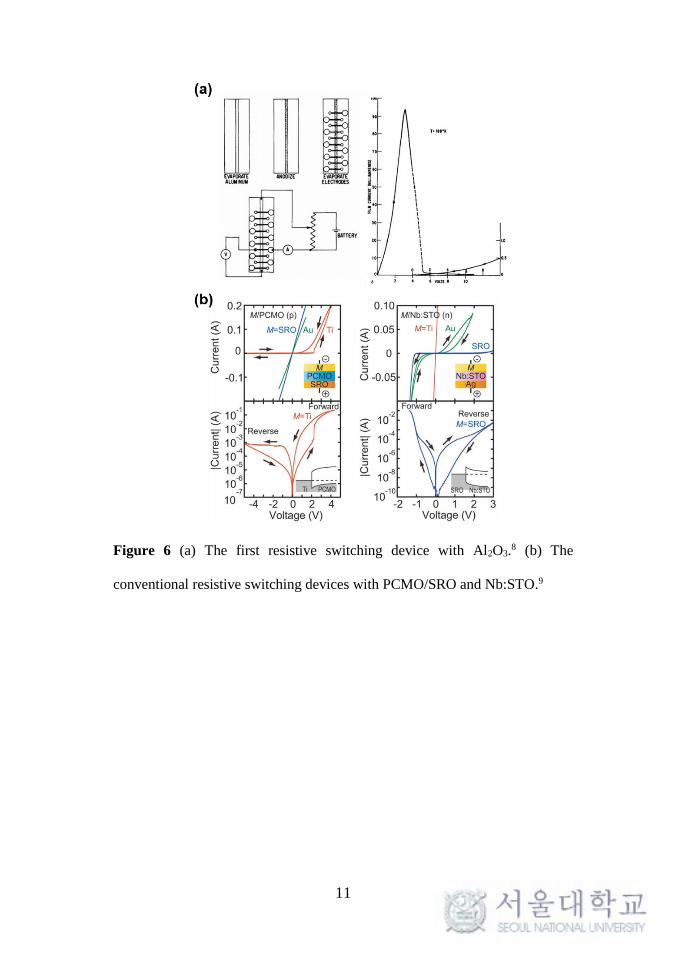
considerable attention. As shown in Figure 6, representative resistive switching
devices based on metal oxides, such as Al2O3, TiO2, Ta2O5-x, SrTiO3, and
Pr0.7Ca0.3MnO3, have all been widely studied.8, 9 Despite continued research into
metal-oxide-based resistive switching memories, this technology is subject to
shortcomings such as a high power consumption, difficult fabrication, and its
unsuitability for flexible/wearable devices.
11
Figure 6 (a) The first resistive switching device with Al2O3.8 (b) The
conventional resistive switching devices with PCMO/SRO and Nb:STO.9

12
1.3. Halide Perovskites
1.3.1 Introduction
Halide perovskites (HPs) with the chemical formula ABX3, ABX4, A2BX4,
An+1Bn,X4n+1, and AnBnX3n+1 consist of a two or three-dimensionally connected
network of corner-sharing metal halide octahedral. Representatively, organic
cations, such as methylammonium or formamidinium occupy the cubo-
octahedral sites, which are each shared by twelve halide anions (Figure 7).
Figure 7 Various composition of halide perovskites of (a) ABX4, (b) A2BX4,(c)
An+1BnX4n+1, (d) An+1BnX3n+1, and (e) AnBnX3n+1.

13
Due to their exotic properties and major advantages in terms of fabrication,
HPs are regarded as being a promising candidate for next-generation resistive
switching devices. HPs possess exotic properties which have not seen before in
other materials: i) a tunable bandgap,10-12 ii) majority carrier control,13, 14 iii) fast
ion migration,15-17 and iv) super flexibility18-20 (Figure 8). The properties of HPs
can be adjusted for application to a given device by changing the composition
of the HPs through the addition of various substitution elements12 as well as
defect engineering.13 Current–voltage (I–V) hysteresis caused by fast ion
migration21, as well as inconsistencies in the forward and reverse scan currents,
can be exploited in memristors and artificial synapse devices in which HPs are
used for non-optoelectronic applications. The high resilience of HPs to bending
deformation originates from their low process temperatures (that are also
compatible with flexible substrates) and their constituent elements.
Figure 8 Exotic properties of halide perovskites. Each figure describes tunable
bandgap, fast ion migration, facile majority carrier control, and flexibility of

14
halide perovskites, respectively. Reproduced with permission. Copyright 2015,
2016, ACS publications,21, 14 2014, AIP publishing LLC,41 and 2017, Royal
Society of Chemistry.53
1.3.2 Unique Properties of HPs
One of the extraordinary properties of HPs is their compositional flexibility,
in that HPs can be constituted using various elements. Those HPs with chemical
formula ABX3 are mainly composed of a three-dimensional framework of
corner-sharing metal halide octahedrals. In the chemical formula ABX3, where
A is an organic cation, B is a metal cation, and X is a halide anion, each A, B,
and X site can be substituted by a diverse range of elements. Based on the
compositional flexibility of the HPs, the tuning of the bandgap is possible
through the substitution of the elements at each site. Moreover, the tuning of
the bandgap can be achieved by controlling the crystallite size and the structure
of the HPs.
The substitution of the A site cation with other alkylammonium cations is one
possible strategy for modifying the bond length between the metal cations in
the B site and the halide anions in the C site. In 1990, Calabrese et al. reported
on layered HPs with (RNH3)2(MeNH3)n-1PbnI3n+1 and
[Me(CH2)8NH3]2(MeNH3)n-1PbnBr3n+1.22 Due to the length of the
alkylammonium cation at the A site, the synthesized HPs exhibited a two-
dimensional layered structure, as well as a red shift of the maximum absorption
peaks from 390 nm to 450 nm as the length of the A site cation was increased.

15
Cao et al. succeeded in bandgap tuning by changing the layer structure from
2D to 3D by controlling the composition ratio of methylammonium (MA) and
butylammonium (BA)23. Previous research into 2D HPs had addressed only a
complete layered structure. They, however, addressed
(CH3(CH2)3NH3)2(CH3NH3)n−1PbnI3n+1 while changing n from 1 to 4 and
infinity (actually MAPbI3).24 The bandgap gradually decreased from 2.24 eV to
1.52 eV with a decrease in the value of n. In addition, the conduction and
valence bands gradually deteriorated from the vacuum level. The results of
calculation-based studies applying density functional theory (DFT) to the 2D
and 3D structures of halide perovskites also point to the possibility of applying
bandgap tunability according to the A-site cations.25 Amat et al. demonstrated
the change in the bandgap of an HP, which can be induced by substituting FA
(1.5 eV), MA (1.55 eV), BA (2.24 eV), and Cs (1.73 eV) to the A-site), by DFT
calculations.12
Another means of bandgap tuning involves the substitution of the metal cation
in the B-site to adjust the bonding between the metal cation in the B-site and
the halide anion in the C site.10 Because the band edge of the HPs is determined
by the metal cation in the B-site, the substitution of a metal cation provides a
means of directly manipulating the valence band maximum and conduction
band minimum.26 For example, Wang et al. reported that both tin (Sn) and lead
(Pb) can be applied as a substitute at the metal sites.27 Due to the change of the
metal cation at B-site, the bandgap of MASnI3 (1.17 eV) is smaller than that of
MAPbI3 (1.55 eV).28

16
Moreover, the calculated bandgaps of MAPbI3 and MASnI3 were reported.
The DFT calculation slightly underestimates the bandgap of the HPs even
though the DFT calculation produces reliable structure and stability values. The
GW calculation provides a precise estimation of the bandgap of the HPs.29 The
calculation produced bandgap values of 1.67 eV (MAPbI3) and 1.10 eV
(MASnI3) which are very close to the experimental values.
In the case of the C sites, the substitution of halide elements such as Cl, Br,
and I was approached mainly by adjusting the ratio of the halide elements.30, 31
In addition to the DFT calculation, HP films were fabricated to observe the
color change.32 As the bandgap of the HP film was increased, the color of the
film changed from black in the case of MAPbI3 (1.5 eV) to yellow for MAPbBr3
(2.2 eV).33, 34
As other strategies, bond angle control related to the cation steric size,
structural distortion, and halogen–hydrogen bonding at the organic-inorganic
interface, have also been reported as a means of engineering the bandgaps of
HPs.35-38 Using these methods, the optical bandgap of the HPs could be
continuously controlled from the mid-infrared to the visible range.
The above approach involved altering the composition of the perovskite to
control the bandgap. However, the bandgap can also be tuned by controlling
the crystallite size of the thin film.11 The time-resolved PL was measured after
preparing samples with MAPbI3 crystallite sizes from 200 nm to 4000 nm. As
a result, the PL spectral position increased from 760 nm to 780 nm, respectively.
It is also assumed that the bandgap decreases slightly.

17
To control the carrier concentration of general silicon-based semiconductors,
several complex processes are employed to activate the carriers, including ion
showers, implantation, and thermal activation. In this case, a doped extrinsic
semiconductor does not adopt an n- or p-type electric property according to the
concentration of the dopants (impurities). However, the doping technique
applied to HPs is slightly different. One of the most interesting characteristics
of HP is that the type of the majority carrier is determined by the cations and
their point defects at the A- and B-sites.13 For example, the defect formation
energy of MAPbI3, as obtained by DFT calculation, revealed that the dominant
native defects are VPb and MAi, given that both defect species have the lowest
defect formation energies (0.29 eV and 0.20 eV, respectively). Since the defect
species that form deep-level traps, such as IPb, IMA, Pbi, and PbI, have high
formation energies (1.53 eV, 1.96 eV, 1.85 eV and 1.97 eV, respectively), this
prevents the formation of these deep-level traps. Schottky defects, such as MAI
and PbI2, are also prevented from forming any traps in the bandgap. However,
the formation of elemental defects, which are derived from Frenkel defects such
as Pb, I, and MA vacancies, is possible.39 The results of the DFT calculations
revealed that the semiconducting type of MAPbI3 is determined by the
concentrations of p-type VPb and n-type MAi, both of which have low defect-
formation energies. However, only p-type doping is allowed for MAPbBr3.40
Since the lattice parameter of MAPbBr3 is smaller than that of MAPbI3, the
formation energy of MAi is high, such that the MAi acts as an n-type dopant.
Therefore, MAPbBr3 only forms shallow traps near the valence band.

18
Manipulating the defect concentration of the HP in the synthesis process is
also accomplished by adjusting the mixing ratios of the organic and inorganic
precursors.41 Both n-type and p-type doping are possible in the HPs. In practical
experiments, the Fermi level was found to change according to the
concentration of the MA cations used for defect engineering. The
methylammonium iodide (MAI) concentration, which was volatile at high
temperatures (> 100 ˚C), was adjusted by thermal annealing of the MAPbI3
films. The change in the Fermi level of the MAPbI3 films was demonstrated by
Hall effect measurements and X-ray photoemission spectroscopy/ultraviolet
photoelectron spectroscopy (XPS/UPS) measurements. As the ratio of the
PbI2/MAI increased as a result of the thermal annealing, the MAPbI3 films were
converted from p-type to heavily n-type, while the bandgaps of the MAPbI3
films were maintained during thermal annealing.14
Another means of controlling the majority carrier concentration involves
utilizing the drift of native point defects, which have low formation energies in
MAPbI3. Due to the inherent properties of the HPs, charge defects or ions easily
migrate under the influence of external biases. In a device with a metal-
MAPbI3-metal structure, the drift of the charged VI•, VPb
’, and VMA’, close to
the contacts, causes band bending and the formation of a p-i-n or n-i-p structure,
which is temporarily induced by applying an electric field.42
Previous research, related to the modulation of the electric properties of
silicon-based semiconductors, has established a means of controlling the
majority carrier concentration by adding dopants (impurities). Since the

19
approaches involving doping and synthesis in HPs differ from those for silicon-
based semiconductors, further studies are required to determine suitable doping
techniques for HPs.
Recently, ion migration in HP has been intensively investigated in terms of
the photocurrent hysteresis.43 The polarity of solar cells can be switched under
external bias regardless of the device configuration, type of HP material, and
electrode materials15. This indicates that ion migration is a general and intrinsic
property of HPs. Ion migration occurs easily and quickly in HPs due to the low
formation energy of the defective ion species and low activation energy
required for ion migration.17,44 Several elements can contribute to ion migration,
including constituent ions such as I−, Pb2+, and MA+ in MAPbI3, defects such
as vacancies, interstitials, and antisites, and other species such as the H+ induced
by material decomposition or contamination.15, 17, 44, 45 Even though ion
migration in HPs has a detrimental effect on the photo-conversion efficiency,
HPs exhibit excellent physical and chemical properties which originate from
the fast ion migration, such as current−voltage (I–V) hysteresis,21, 48 a
switchable photovoltaic effect,42 giant dielectric constant,47 photo-induced
phase separation,48 and a photo-induced self-poling effect.15, 49 These numerous
phenomena are very interesting and point to the wide range of possibilities of
the HP-based electronic devices.
The constitutent ions in HP can contribute to ion migration through schottky
defects given their low activation energy (EA) for migration.15 The EA of ion
migration indicates how easily ions move in a solid material. In MAPbI3, I− ions

20
are the most mobile ions due to their being closer to the neighboring I−
vacancies (around 4.46 Å ) than either the MA+ or Pb2+ ions (around 6.28 Å ).17
Several first-principle calculations on EA for MAPbI3 have been reported
allowing a comparison of the EA values required for the migration of I−, Pb2+,
and MA+ ions in MAPbI3.44, 50 Although there are subtle differences in the EA
values, all the results showed that the I− ions are more mobile than either the
MA+ and Pb2+ ions due to the smallest EA values of the I− ions. Eames et al.
demonstrated the calculated EA values for I−, Pb2+, and MA+ ions in MAPbI3.17
They showed that the I− ions had the lowest EA values of 0.58 eV, which are
migrating along the iodine edges of the PbI6 octahedron. MA+ and Pb2+ ions
had EA values of 0.84 eV and 2.31 eV, respectively.
The high ionicity of HP can be caused by unsual defect property. The defects,
such as vacancies, interstitials, and antisites, are mobile species which can
participate in ion migration under external bias. There are no significant
differences in the calculation of the formation energies of the interstitial defects
and the activation energies required for ion migration for the I− (0.23-0.83 eV,
0.58 eV) and MA+ ions (0.20-0.93 eV, 0.84 eV).13 Thus, the ion migration
through Frenkel defects should be considered. Additional species, such as H+
ions, can also affect ion migration through Frenkel defects, given that they are
the smallest in size. Low EA value of H+ ion migration along a transient
hydrogen bond between two equatorial iodides was calculated about to be 0.29
eV.45

21
The rotation of organic cation sites may contribute to the I–V hysteresis caused
by ion migration. The electric polarization can be tuned by modifying the
organic cations. The relationship between the rotation of organic cation sites
and ferroelectricity under electric field was analyzed according to the organic
cation sites (NH4+, MA, FA) through DFT calculations.51 In the relaxed state,
the organic cation is tilted through 30˚ in the lattice and can be aligned under
external bias. The rotation of the organic cation sites can occur easily with a
low required energy of about 0.37 eV.52
As HPs are good ionic conductors, they can exhibit fast ion migration. Various
factors, such as constitution ions, defects, and cation rotation, can affect the ion
migration. This fast ion migration, which is suppressed in solar cells, enable the
application of the material to memristors and artificial synapse devices beyond
optoelectronics.
As wearable devices are set to become a major electronics platform, there is
an increasing demand for flexibility as a required material property. Moreover,
it must be possible to synthesize the active materials of flexible devices at low
temperatures, since polymer substrates, which are commonly used in flexible
devices, cannot withstand high-temperature processes. HPs offer a significant
advantage in this respect. The mechanical flexibility of the material itself and
the low temperature of the process together enable the application of the
material to flexible devices.
Typical HPs such as MAPbI3 have mechanically organic characteristics due
to their organic cation elements which have weak interactions between organic

22
elements. Moreover, the annealing temperature of HPs usually does not exceed
150 ˚C. Therefore, a highly flexible polymer substrate with a lower process
temperature than metal foil or thin flexible glass can be used for the HP-based
flexible devices.
There have been many studies involving repeated bending test on the HP-
based solar cells and memory devices, exhibiting the outstanding mechanical
flexibility of the materials. By Yoon et al., high-efficiency HP-based solar cells
were demonstrated to have excellent electrical reliability and mechanical
stability against bending test.53 By using graphene as the conducting anode
instead of indium-tin-oxide, the devices exhibited an extremely stable electrical
reliability that over 85% of initial efficiency was maintained even after 5000
bending cycles with a bending radius of 2 mm. In addition, no significant cracks
or variations in the sheet resistance were observed with the graphene-based
solar cells during the bending tests. For other electronic devices, Gu et al.
reported on a flexible HP-based resistive switching memory devices, formed
on a plastic substrate.54 The electrical properties of the memory devices were
maintained over 100 bending cycles with a bending radius of 1.5 cm. Thus,
excellent mechanical stability as well as electrical reliability can also be seen
in a HP-based memory devices.
Super-flexibility can be realized in HP-based electronic devices, which is
impossible with conventional semiconductors. Mechanical flexibility and low-
temprerature process of the HPs allow various types of substrates including
polymer, mainly used for flexible devices. Recently, HP-based electronic

23
devices, solar cells and resistive switching memory devices, were demonstrated
with excellent mechanical stability as well as electrical reliability. Thus, HP-
based electronic devices are expected to be applied to many flexible and
wearable devices in the near future.

24
1.4 References
1. Jet Propulsion Laboratory, NASA, https://voyager.jpl.nasa.gov/golden-
record
2. J. Gantz, D. Reinsel, The Digital Universe In 2020: Big Data, Bigger
Digital Shadows, and Biggest Growth in the Far East,
http://www.emc.com/collateral/analyst-reports/idc-the-digital-universe-
in-2020.pdf
3. K.-T. Park et. al. J. Solid-State Circuits 2015, 50, 204.
4. S. W. Park, Prospect for New Memory Technology, 2012 Flash Memory
Summit,
https://www.flashmemorysummit.com/English/Collaterals/Proceedings/2
012/20120821_Keynote2_Park.pdf
5. S. Ver-Bruggen, 3D NAND: To 10nm and beyond, 2014 Semiconductor
Manufacturing and Design, http://semimd.com/blog/tag/3d-dram/
6. International Technology Roadmap for Semiconductors(ITRS), KIPO,
KISTI, ITRS, IEDM.
7. Waser, R., Nanoelectronics and Information Technology : Advanced
Electronic Materials and Novel Devices. 3rd ed. Wiley-VCH: Weinheim,
2012, 696-700 .
8. T. W. Hickmott, J. Appl. Phys. 1962, 33, 2669.
9. A. Sawa, Mater. Today. 2008, 11, 28-36.
10. A. Walsh, J. Phys. Chem. C 2015, 119, 5755.
11. V. D'Innocenzo, A. R. Srimath Kandada, M. De Bastiani, M. Gandini, A.
Petrozza, J. Am. Chem. Soc. 2014, 136, 17730.
12. A. Amat, E. Mosconi, E. Ronca, C. Quarti, P. Umari, M. K. Nazeeruddin,
M. Gratzel, F. De Angelis, Nano. Lett. 2014, 14, 3608.
13. W.-J. Yin, T. Shi, Y. Yan, Appl. Phys. Lett. 2014, 104, 063903.
14. C. Bi, Y. Shao, Y. Yuan, Z. Xiao, C. Wang, Y. Gao, J. Huang, J. Mater.
Chem. A 2014, 2, 18508.
15. Y. Yuan, J. Huang, Acc. Chem. Res. 2016, 49, 286.
16. A. M. Leguy, J. M. Frost, A. P. McMahon, V. G. Sakai, W. Kochelmann,
C. Law, X. Li, F. Foglia, A. Walsh, B. C. O'regan, Nat. Commun. 2015, 6,
7124.

25
17. C. Eames, J. M. Frost, P. R. Barnes, B. C. O'Regan, A. Walsh, M. S. Islam,
Nat. Commun. 2015, 6, 7497.
18. P. Docampo, J. M. Ball, M. Darwich, G. E. Eperon, H. J. Snaith, Nat.
Commun. 2013, 4, 2761.
19. J. You, Z. Hong, Y. M. Yang, Q. Chen, M. Cai, T.-B. Song, C.-C. Chen,
S. Lu, Y. Liu, H. Zhou, ACS Nano 2014, 8, 1674.
20. B. J. Kim, D. H. Kim, Y.-Y. Lee, H.-W. Shin, G. S. Han, J. S. Hong, K.
Mahmood, T. K. Ahn, Y.-C. Joo, K. S. Hong, N.-G. Park, S. Lee, H. S.
Jung, Energy Environ. Sci. 2015, 8, 916.
21. H. J. Snaith, A. Abate, J. M. Ball, G. E. Eperon, T. Leijtens, N. K. Noel,
S. D. Stranks, J. T. Wang, K. Wojciechowski, W. Zhang, J. Phys. Chem.
Lett. 2014, 5, 1511.
22. J. Calabrese, N. Jones, R. Harlow, N. Herron, D. Thorn, Y. Wang, J. Am.
Chem. Soc. 1991, 113, 2328.
23. D. H. Cao, C. C. Stoumpos, O. K. Farha, J. T. Hupp, M. G. Kanatzidis, J.
Am. Chem. Soc. 2015, 137, 7843.
24. C. C. Stoumpos, D. H. Cao, D. J. Clark, J. Young, J. M. Rondinelli, J. I.
Jang, J. T. Hupp, M. G. Kanatzidis, Chem. Mater. 2016, 28, 2852.
25. T. Umebayashi, K. Asai, T. Kondo, A. Nakao, Phys. Rev. B 2003, 67,
155405.
26. F. Hao, C. C. Stoumpos, R. P. Chang, M. G. Kanatzidis, J. Am. Chem. Soc.
2014, 136, 8094.
27. S. Wang, D. B. Mitzi, C. A. Feild, A. Guloy, J. Am. Chem. Soc. 1995, 117,
5297.
28. C. C. Stoumpos, C. D. Malliakas, M. G. Kanatzidis, Inorg. Chem. 2013,
52, 9019.
29. P. Umari, E. Mosconi, F. De Angelis, Sci. Rep. 2014, 4, 4467.
30. D. M. Jang, K. Park, D. H. Kim, J. Park, F. Shojaei, H. S. Kang, J. P. Ahn,
J. W. Lee, J. K. Song, Nano Lett. 2015, 15, 5191.
31. E. Mosconi, A. Amat, M. K. Nazeeruddin, M. Grätzel, F. De Angelis, J.
Phys. Chem. C 2013, 117, 13902.
32. J. Even, L. Pedesseau, J.-M. Jancu, C. Katan, J. Phys. Chem. Lett. 2013, 4,
2999.
33. J. H. Noh, S. H. Im, J. H. Heo, T. N. Mandal, S. I. Seok, Nano. Lett. 2013,
13, 1764.

26
34. S. A. Kulkarni, T. Baikie, P. P. Boix, N. Yantara, N. Mathews, S.
Mhaisalkar, J. Mater. Chem. A. 2014, 2, 9221.
35. M. R. Filip, G. E. Eperon, H. J. Snaith, F. Giustino, Nat. Commun. 2014,
5, 5757.
36. J. L. Knutson, J. D. Martin, D. B. Mitzi, Inorg. Chem. 2005, 44, 4699.
37. S. Sourisseau, N. Louvain, W. Bi, N. Mercier, D. Rondeau, F. Boucher, J.-
Y. Buzaré, C. Legein, Chem. Mater. 2007, 19, 600.
38. N. Mercier, S. Poiroux, A. Riou, P. Batail, Inorg. Chem. 2004, 43, 8361.
39. J. Kim, S. H. Lee, J. H. Lee, K. H. Hong, J. Phys. Chem. Lett. 2014, 5,
1312.
40. T. Shi, W.-J. Yin, F. Hong, K. Zhu, Y. Yan, Appl. Phys. Lett. 2015, 106,
103902.
41. Q. Wang, Y. Shao, H. Xie, L. Lyu, X. Liu, Y. Gao, J. Huang, Appl. Phys.
Lett. 2014, 105, 163508.
42. Z. Xiao, Y. Yuan, Y. Shao, Q. Wang, Q. Dong, C. Bi, P. Sharma, A.
Gruverman, J. Huang, Nat. Mater. 2015, 14, 193.
43. Y. Shao, Z. Xiao, C. Bi, Y. Yuan, J. Huang, Nat. Commun. 2014, 5, 5784.
44. J. Haruyama, K. Sodeyama, L. Han, Y. Tateyama, J. Am. Chem. Soc. 2015,
137, 10048.
45. D. A. Egger, L. Kronik, A. M. Rappe, Angew. Chem. Int. Ed. 2015, 54,
12437.
46. E. L. Unger, E. T. Hoke, C. D. Bailie, W. H. Nguyen, A. R. Bowring, T.
Heumüller, M. G. Christoforo, M. D. McGehee, Energy Environ. Sci. 2014,
7, 3690.
47. E. J. Juarez-Perez, R. S. Sanchez, L. Badia, G. Garcia-Belmonte, Y. S.
Kang, I. Mora-Sero, J. Bisquert, J. Phys. Chem. Lett. 2014, 5, 2390.
48. C. G. Bischak, C. L. Hetherington, H. Wu, S. Aloni, D. F. Ogletree, D. T.
Limmer, N. S. Ginsberg, Nano Lett. 2017, 17, 1028.
49. W. Zhang, V. M. Burlakov, D. J. Graham, T. Leijtens, A. Osherov, V.
Bulović, H. J. Snaith, D. S. Ginger, S. D. Stranks, Nat. Commun. 2016, 7,
11683.
50. J. M. Azpiroz, E. Mosconi, J. Bisquert, F. De Angelis, Energy Environ.
Sci. 2015, 8, 2118.

27
51. J. M. Frost, K. T. Butler, F. Brivio, C. H. Hendon, M. Van Schilfgaarde,
A. Walsh, Nano. Lett. 2014, 14, 2584.
52. R. Gottesman, E. Haltzi, L. Gouda, S. Tirosh, Y. Bouhadana, A. Zaban, E.
Mosconi, F. De Angelis, J. Phys. Chem. Lett. 2014, 5, 2662.
53. J. Yoon, H. Sung, G. Lee, W. Cho, N. Ahn, H. S. Jung, M. Choi, Energy
Environ. Sci. 2017, 10, 337.
54. C. Gu, J. S. Lee, ACS Nano 2016, 10, 5413.

28
Chapter 2
The First High Performance HP-based RS memory
Quote
Aristotle
"Everything that is in motion must be moved by something.”

29
2.1. Introduction
Organolead halide perovskites (OHPs) with the chemical formula ABX3
consist of a three-dimensionally connected network of corner-sharing lead
halide octahedral. Organic cations, such as methylammonium or
formamidinium occupy the cubo-octahedral sites, which are each shared by
twelve halide anions. Due to their inherent hybrid structure, OHPs show
unusual electrical and optical properties such as high light absorption and
structural and compositional flexibility1-4. Mixed ionic–electronic conduction
behavior is found in OHPs, suggesting ion migration plays a role in devices
based on the materials. Methylammonium lead iodide (CH3NH3PbI3) has
received attention as a light absorber5-7 and charge transport8,9 material for solar
cells. Its superior properties, such as a large light absorption coefficient, a small
exciton binding energy10 and a balanced long-range charge diffusion length11
make the material ideal for photovoltaic applications.
Here, we report an ultralow electric field and high ON/OFF ratio resistive
switching behavior of solution-processed OHP films, which is exploited for
multilevel data storage. Ag/CH3NH3PbI3/Pt cells exhibit electroforming-free
resistive switching at an electric field of 3.25 ⅹ 103 V/cm for distinguishable
four ON-state resistance levels. Density functional theory calculations show
that the migration of iodine interstitials and vacancies with low activation
energies is responsible for the low electric field resistive switching via filament
formation and annihilation.
30
One of the interesting phenomena that inspired this study is the hysteretic
current-voltage characteristics exhibited by CH3NH3PbI3 due to the build-up of
space charges close to the contacts originating from ionic displacement.12,13
Xiao et al.12 showed that photocurrent direction in CH3NH3PbI3 films could be
switched repeatedly by applying a small electric field of < 1 V/μm, which was
explained by the formation of reversible p–i–n structures induced by ion drift
in the perovskite layer. Although the exact defect nature is still elusive, recent
studies have shown that negatively charged Pb and CH3NH3 vacancies and
positively charged I vacancies are the predominant ionic species.14, 15 More
excitingly, the rotational motion of the A-site organic cation can provide
structural flexibility and even ferroelectric behavior on the nanoscale.16, 17
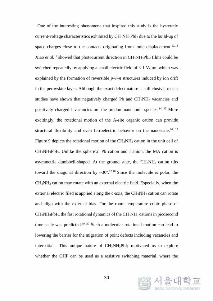
Figure 9 depicts the rotational motion of the CH3NH3 cation in the unit cell of
CH3NH3PbI3. Unlike the spherical Pb cation and I anion, the MA cation is
asymmetric dumbbell-shaped. At the ground state, the CH3NH3 cation tilts
toward the diagonal direction by ~30o.17,18 Since the molecule is polar, the
CH3NH3 cation may rotate with an external electric field. Especially, when the
external electric filed is applied along the c-axis, the CH3NH3 cation can rotate
and align with the external bias. For the room temperature cubic phase of
CH3NH3PbI3, the fast rotational dynamics of the CH3NH3 cations in picosecond
time scale was predicted.19, 20 Such a molecular rotational motion can lead to
lowering the barrier for the migration of point defects including vacancies and
interstitials. This unique nature of CH3NH3PbI3 motivated us to explore
whether the OHP can be used as a resistive switching material, where the

31
electrochemical motion of the charged ions and/or the structural phase
transition play a role.21-25
Figure 9 A-site molecular rotational motion in a unit cell of CH3NH3PbI3.
In this chapter, I report extraordinary resistive switching behavior of organic-
inorganic hybrid perovskite thin films under extremely low electric fields.
Typical I–V characteristics of solution-processed 400-nm-thick CH3NH3PbI3
thin films sandwiched with Ag top and Pt bottom electrodes exhibit resistive
switching with ON/OFF ratio more greater than 106 and SET voltages below
0.15 V, leading to demonstrating four-level resistance states for multilevel data
storage. We performed first-principles calculations to describe that the ultralow
electric field bipolar resistive switching properties of the CH3NH3PbI3 thin
films.
HI Pb C N
E→

32
2.2. Experimental Procedures
Materials preparation: Methylammonium iodide (CH3NH3I) was prepared by
reacting methylamine (7.46 mL, 40% in methanol, TCI) and hydriodic acid (10
mL, 55% in water, ACROS ORGANICS). Reacting solution was stirred at 0
for 2h. The solvent was removed by rotary evaporation at 50 for 1h. The
precipitate (CH3NH3I) was dissolved in ethanol and mixing diethyl ether
(Daejung Chemicals) for recrystallization. This recrystallization process was
repeated twice. After recrystallization, product (CH3NH3I) dried in vacuum
oven at 60 for 24 h.
Film Formation and MIM cell fabrication: Pt/Ti-coated substrates were
prepared by electron beam evaporation. Firstly, a 20-nm-thick Ti thin film was
deposited on SiO2 substrates using e-beam evaporator for the better adhesion
of the Pt layer and a 50-nm-thick Pt thin film was sequently deposited on the
substrates. The Pt-coated substrates were washed by acetone, isopropanol,
deionized water under ultrasonication and then treated by air plasma cleaner for
5 min just prior to the synthesis of CH3NH3PbI3 films on the substrates.
CH3NH3PbI3 films were synthesized on Pt/Ti/SiO2/Si substrates. The
perovskite precursor solution was prepared by mixing methylammonium iodide
(MAI) powders and PbI2 in various molar ratios (MAI/ PbI2 ratios from 0.9 to
1.1) in anhydrous N,N-dimethylformamide (DMF) for overall concentration of
40 wt%. To deposit CH3NH3PbI3 perovskite film, the resulting solution was
spin-coated on Pt/Ti/SiO2/Si and glass substrates at 4000 rpm for 60 s. During
the spin coating (5 s after spinning), anhydrous toluene was dropped onto the

33
center of the substrate for better morphology of CH3NH3PbI3 perovskite film.
After spin coating, film was annealed on a hot plate at 70 for 30 min. Ag, Ni
and Au were selected as top electrodes of resistive switching device. 50 μm
50 μm, 200 μm 200 μm and 400 μm 400 μm of top electrodes were
deposited on CH3NH3PbI3 perovskite film by e-beam evaporation method with
the shadow mask. The evaporation was performed at 1 10-6 Torr of pressure
and room temperature.
Device characterization: For XRD measurements, a CH3NH3PbI3 perovskite
film was coated on a glass substrate. The XRD pattern was obtained from X-
Ray Diffractometer (BRUKER MILLER Co., D8-Advance) with Cu Kα
radiation (λ = 1.54056 Å). XRD data was recorded at room temperature in the
range of 10−60° of 2θ range with a step size of 0.02° and scan speed of 2 degree
per minute. The surface and cross sectional images were obtained from Field
Emission Scanning Electron Microscope (ZEISS, MERLIN Compact). Images
were obtained with an in-lens secondary electron detector at 1kV accelerating
voltage. The I−V characteristics were measured by Agilent 4156C
semiconductor analyzer with direct current (DC) voltage sweeping mode.
Resistive switching by alternating voltage pulses were measured by the Agilent
4156C semiconductor analyzer. All of the electrical properties were measured
in a vacuum chamber (6 10-2 Torr). To observe conduction mechanism in the
CH3NH3PbI3 films, the conductance of CH3NH3PbI3 films coated on
Ag/Ti/SiO2/Si substrate at room temperature was measured by CAFM (Park

34
systems XE100) in a glovebox, which was Ar atmosphere. A platinum coated
STM-type tip was used to substitute platinum counter electrodes.
DFT calculation: The first-principles density functional theory (DFT)
calculations based on the projected augmented wave (PAW) pseudopotential
were performed using the Vienna Ab-initio simulation package (VASP) code.
The nudged elastic band (NEB) method was employed in computing the
activation energy along the migration path. As the present DFT study assumes
the zero Kelvin temperature condition, the orthorhombic phase of the
CH3NH3PbI3 was used for the calculation. The supercell include 48 atoms
(orthorhombic unit cell) for the iodine vacancy and 182 atoms (2 2 1
orthorhombic cell) for the interstitial iodine. The cutoff energy for plane-wave
basis set was chosen to be 550 eV and the gamma point was sampled in the
Brillouin-zone integration. Atomic positions were relaxed until the forces were
reduced below 0.02 eV/Å .

35
2.3. Results and Discussion
The CH3NH3PbI3 thin films used for this study were 400-nm-thick and the
average grain size was approximately 133 nm. Despite a large variation in grain
size, the CH3NH3PbI3 thin films were uniformly spin-coated on Pt/Ti/SiO2/Si
substrates. Figure 10 shows that the CH3NH3PbI3 thin film is polycrystalline
and of a single-phase organolead halide as shown in the X-ray diffraction
pattern in Figure 10.17
Figure 10 (a) Plane-view and cross-sectional SEM images of a 400 nm-thick
CH3NH3PbI3 thin film on Pt/Ti/SiO2/Si substrate. (b) X-ray diffraction pattern
of a CH3NH3PbI3 film on SiO2/Si substrate. Red lines are XRD pattern from
Ref. 17
After spin-coating and annealing of the CH3NH3PbI3 thin film, MIM vertical
structure cells were fabricated by depositing 50 μm ⅹ 50 μm top metal
electrodes such Ag, Ni and Au using a shadow mask and an electron beam
evaporator. To achieve pinhole-free CH3NH3PbI3 films with uniform
thicknesses we used a rapid crystallization method using N,N-
dimethylformamide and toluene as the solvent for the OHP precursors
(CH3NH3I and PbI2). Because CH3NH3PbI3 and the precursors are minimally
(a) (b)

36
soluble in toluene, the addition of toluene significantly reduced the solubility
of CH3NH3PbI3 in the mixed solution and rapid crystallization occurred. As a
result of the rapid crystallization, we obtained uniform and pinhole-free
CH3NH3PbI3 films.26 Using the pinhole-free MIM cells (Figure 11), we
succeeded in measuring insulating ground states from the solution-processed
CH3NH3PbI3 films.
Figure 11 SEM images of the vertical structure devices. (a-c), Each device has
(a) Ag, (b) Ni, (c) Au electrodes. The thickness of CH3NH3PbI3 thin film is
about 320-400nm. We adopted two types of metals, such as Ag and Ni to the
top electrodes to investigate the resistive switching properties. The minimum
thickness of the top electrodes is about 50 nm. (d) Schematic of the
metal/CH3NH3PbI3/metal vertical structure for resistive switching.
A typical I–V curve of the Ag/CH3NH3PbI3/Pt cells is shown in Figure 12a.
With the applied voltage sweep of 0 V → + 0.15 V → 0 V → - 0.15 V → 0 V,
37
the measured current values were plotted on a logarithmic scale. The hysteresis
loop indicates that the device exhibits bipolar switching.21,27 Initially, the device
was in an insulating (high resistance) state (HRS) with current levels of 10-10–
10-9 A. The current increased abruptly when the applied voltage was
approximately 0.13 V. Then, the device retained a conducting (low resistance)
state (LRS) with current levels near 10-3 A. It should be noted that the current
density for the LRS state is over hundreds of times higher than the photocurrent
densities of the CH3NH3PbI3 films studied for photovoltaic applications. The
equivalent electric field for the onset of the low resistance state is 3.25 103
V/cm for the 400-nm-thick CH3NH3PbI3 film. The transition between HRS
(OFF state) and LRS (ON state) is switchable and the ON/OFF ratio is as high
as ~106. The CH3NH3PbI3 devices do not require electroforming, even though
the thickness of the CH3NH3PbI3 thin film is approximately 400 nm. In Figure
12b, The I–V curves do not show remarkable variation in the SET voltages,
indicating the electroforming-free characteristic of the CH3NH3PbI3-based
MIM cells. It is interesting that the operation electric field (3.75 103 V/cm) is
comparable to the applied electric field for the switchable photovoltaic effect
in CH3NH3PbI3–based devices (1.2 104 V/cm), where the electrical
programming with optical reading out was explained by the migration of defect
ions.

38
Figure 12 Resistive switching properties of Ag/CH3NH
3PbI
3/Pt cells. (a)
Typical current-voltage (I-V) characteristic of Ag/CH3NH
3PbI
3/Pt cells. (b) I-V
characteristics of a Ag/CH3NH
3PbI
3/Pt cell from 5 initial voltage sweeps. SET
voltage is + 0.15 V and RESET voltage is – 0.15 V.
Resistive switching with voltage pulses is also possible for the device (Figure
13a). At voltages of 0.15 V (200-ms pulse width), the CH3NH3PbI3-based
MIM cell showed reproducible resistive switching with ON/OFF ratios above
106 over 350 cycles. We measured 50 Ag/CH3NH3PbI3/Pt cells for resistive
switching with writing voltages of 0.15 V (250-ms pulse width). As plotted
in Figure 13b, the 50 electrodes showed an average ON/OFF ratio of 1.12 106
without considerable deviations.

39
Figure 13 (a) Reversible resistive switching measured with a writing voltage
of 0.15 V and a reading voltage of 0.02 V. The pulse width of the writing
voltage was 200 ms. (b) High and low resistance states for 50 different cells.
The average on/off ratio is calculated to be 1.12 x 10⁶.
The reproducibility of the uniform HRS and LRS levels of many cells
indicates that the CH3NH3PbI3-based MIM cells are feasible for reliably high
ON/OFF ratio resistive switching with a low electric field. The typical retention
characteristics of the ON and OFF states for an Ag/CH3NH3PbI3/Pt cell showed
that the ON state is stable up to 11000 s (Figure 14).
Figure 14 Retention characteristics of the Ag/CH3NH3PbI3/Pt/SiO2/Si device.
The SET and RESET voltages of the CH3NH3PbI3 devices depends on the
ratio of methylammonium iodide (MAI) and lead iodide (PbI2) precursors. The

40
operation voltage is less than ± 0.15 V when the MAI/ PbI2 ratio is 1. When the
MAI/ PbI2 ratio is 1.1 or 0.9, the CH3NH3PbI3 thin films are metallic and
hysteretic I-V characteristics cannot be obtained (Figure 15).
Figure 15 (a) Stoichiometry-dependent X-ray diffraction patterns of a
CH3NH3PbI3 films by the controlling of the ratio of methylammonium and lead
iodide. (Black line-exact stoichiometry, green line-methylammonium iodide
rich, blue line-lead iodide rich, red line-Ref 20.). In the blue line, peaks for PbI2
appear at 12.67, 25.49, 38.59, and 52.33 degrees (Red stars, JCPDS No. 00-
007-0235). (b) I-V characteristics of the CH3NH3PbI3 thin films are synthesized
by the ratio of methylammonium and lead iodide is 1:1. (c) Methylammonium
iodide rich and (d) Lead iodide rich. The thickness of the thin films is fixed to
320-350 nm.

41
To understand the current conduction mechanism at the interface between the
top electrode and the CH3NH3PbI3 layer, we highlighted the I–V curves for the
ON and OFF states of the Ag/CH3NH3PbI3/Pt and Ni/CH3NH3PbI3/Pt cells
(Figure 15a). For both cells which adopted Ag and Ni top electrodes, the OFF
state I–V curves show linear and non-linear regions, indicating that space-
charge limited conduction is dominant. The ON state I–V curves exhibit
perfectly ohmic behavior, suggesting the formation of highly conducting paths
between the top and bottom electrodes. The dependence of the current levels
for the ON and OFF states of Ag/CH3NH3PbI3/Pt cells on the area of the top
electrode was investigated (Figure 15b). Although the area of the top electrode
was increased 64 fold, the current levels for the ON states did not increase,
whereas the current levels for the OFF states varied considerably at the nA scale.
This result indicates that the conducting paths for the ON states are localized,
namely, filamentary.21, 22, 28,29
Figure 16 Dependence of the top electrodes and electrode area. (a) Linear-scale
I-V characteristics of the ON (LRS) and OFF states. (b) Dependence of ON and

42
OFF state current levels on the area of Ag top electrodes for Ag/CH3NH3PbI3/Pt
cells.
Ag is known to be relatively active metal than Ni and Au. MIM cells with Ag
top electrodes showed operation voltages less than ± 0.14 V (Figure 17a),
whereas cells with Ni and Au top electrodes showed higher operation voltages
over ± 0.4 V (Figure 17b and c). It is suggested that the electrochemical activity
of the top electrode plays a role in triggering the abrupt resistive switching
behavior.
Figure 17 Dependence of the top electrodes. (a) Ag/CH3NH3PbI3/Pt, (b)
Ni/CH3NH3PbI3/Pt and (c) Au/CH3NH3PbI3/Pt cells. The cells adopt (a) Ag, (b)
Ni and (c) Au top electrodes show hysteretic I-V curves which are applicable
to resistive switching. The cells with Ag top electrodes are switchable in low

43
SET/RESET voltage. With high SET voltage (> 0.25 V), these cells could not
be turned off perfectly. The cells adopt Ni and Au top electrodes had relatively
higher SET voltages (> 0.3 V).
We performed conducting atomic force microscopy (CAFM) on a
CH3NH3PbI3 film on Ag/Ti/SiO2 substrate in order to determine whether the
pre-existing grain boundaries or non-uniformity in the thickness play a role in
forming conducting filaments for the ON states. The 400-nm-thick film was
granular. The grain size varied from 300 nm to 1000 nm and the rms roughness
is about 40 nm with a maximum peak-to-valley depth of 60 nm, as shown in
Figure 18.
Figure 18 Scanning probe microscopy images of CH3NH3PbI3 thin films. (a) A
topological AFM image of the CH3NH3PbI3/Ag structure. The scale of bars is
500 nm. The tip moves 3 µm through the blue dotted line to measure the
roughness by the distance (down).

44
At a bias of 0.1 V on the probe tip, the CH3NH3PbI3 film was uniformly
insulating with current levels of several tens of nA (Figure 19a). The film
became conducting with current levels of ~50 μA at a bias of 1 V (Figure 19b).
The whole area of the film was conducting regardless of the morphology,
suggesting that conducting filaments which could not be visualized with the
AFM tip of ~50 nm radius were formed through the CH3NH3PbI3 film under an
external bias.
Figure 19 Scanning probe microscopy images of CH3NH3PbI3 thin films. (a),
(b) CAFM images of a CH3NH3PbI3/Ag structure with platinum coated tip
biases of (a) 0.1 V and (b) 1 V. The scale of bars is 500 nm. The tip moves
through the blue dotted line to measure the current vs the distance (down).

45
We could vary the grain size in the CH3NH3PbI3 film from 70 nm to 600 nm by
controlling the annealing condition of the film (Table 2).
Annealing
temperatu
re (°C)
Time
(min)
Annealing
atmosphere
Average
grain
size
(nm)
Standard
deviation
of grain
size (nm)
Endurance
(cycles)
Sample 1 100 40 DMF 601.30 ±74.17 0
Sample 2 100 40 Ambient 147.06 ±22.86 4
Sample 3 70 40 Ambient 103.35 ±10.47 50
Sample 4 70 1 Ambient 89.45 ±6.75 38
Sample 5 No
annealing N/A Ambient 71.15 ±5.39 17
Table 2 Five CH3NH3PbI3 films with different grain sizes by controlling
annealing condition.

46
Combined with X-ray diffraction data, endurance measurements revealed that
obtaining the films with the constitute composition without secondary phases
is more important than tailoring the grain size (Figure 20 and 21).
Figure 20 X-ray diffraction patterns and SEM images for CH3NH3PbI3 films
synthesized using annealing conditions. (a) Sample 1 (100 °C, 40mins, DMF),
(b) Sample 2 (100 °C, 40 mins, ambient), (c) Sample 3 (70 °C, 40 mins,
ambient), (d) Sample 4 (70 °C, 1 min, ambient), (f) Sample 5 (No heat treatment,
ambient). The diffraction peak near 12.6° for PbI2 (Red star, (a)) is absent. The
insets of each XRD pattern are plain-view SEM images of each sample.

47
Figure 21 Number of cycles with ON/OFF ratio over 106 from endurance
measurements (total 50 number of cycles) for CH3NH3PbI3 films with different
grain sizes.
To compare the extraordinary resistive switching properties of the
CH3NH3PbI3-based devices with those of conventional resistive switching
devices, we plotted the ON/OFF ratio vs. the reciprocal of the electric field for
SET (1/ESET) in Figure 21.20,29-46 Binary transition metal oxides, such TiO2 and
TaOx, the most widely studied materials for resistive switching, show varied
ON/OFF ratios and relatively low 1/ESET values (< 1 10-5 cm/V). Inorganic
perovskites, such as SrTiO3, exhibit low 1/ESET values near ~10-5 cm/V with
relatively low ON/OFF ratios. Organic materials demonstrate the lowest 1/ESET
values, showing large variations in the ON/OFF ratios. The OHP CH3NH3PbI3
has a relatively high ON/OFF ratio of > 106 and the highest 1/ESET value, which
is one order of magnitude higher than those of chalcogenides.

48
Figure 22 Comparison with various resistive switching materials. The ON/OFF
ratio of resistive switching devices including the CH3NH3PbI3–based cells.
We note that the formation of conducting filaments by Ag migration though
the 400-nm-thick CH3NH3PbI3 film is rare for a SET voltage as low as 0.13 V,
which corresponds to 3.25 103 V/cm. Conventional Ag migration resistive
switching memories typically require much higher electric fields for SET (> 1
105 V/cm) and undergo electroforming under even higher electric fields.21
This suggests that charged defect ions (point defects) in the film itself rather
metal ions are responsible for the ultralow electric field resistive
switching.21,22,24 To reveal the origin of the resistive switching in the
CH3NH3PbI3-based cells, we studied the migration energies of representative
point defects in CH3NH3PbI3 with density functional theory (DFT) calculations,
assuming that the hysteretic I–V characteristics are caused by the migration of
charged point defects.47-51 CH3NH3PbI3 has abundant, intrinsic, shallow point
defects. We consider two point defects, VI• and iI
′ (split interstitial), which are
thermodynamically stable and likely to be highly mobile.8,9,12,17,52 The

49
generalized gradient approximation functional is adopted and the migration
barrier is calculated using the nudged elastic band method. As shown in Figure
23, VI• and iI
′ can migrate with low activation energies of 0.25 eV and 0.15 eV,
respectively. These energies are significantly lower than the migration barriers
of VO•• in TiO2 (1.15 eV) and SrTiO3 (1.22 eV) which are widely used in
resistive switching devices.53,54 Therefore, we suggest that the low switching
voltages of the CH3NH3PbI3 cells are due to the small migration barriers of the
charged anion defects.
Figure 23 DFT calculation for native point defects in CH3NH3PbI3. (a)
Schematic migration paths of VI• (left) and Ii
´ (right) in the unit cell of
CH3NH3PbI3. The center of the split interstitial is moved to adjacent I site, and
the direction of the split rotates to another [110] direction. (b) DFT calculation
about the activation energy for the movements of VI• and Ii′ to the next sites.
To provide plausible explanation for the resistive switching in the
Ag/CH3NH3PbI3/Pt cells, we illustrated the procedure of filament formation
and annihilation due to the migration of iI′ (Figure 24).

50
Figure 24 Schematic of filamentary resistive switching behaviour in
Ag/CH3NH3PbI3/Pt cells by defect ion migration. (a) Initial state of
Ag/CH3NH3PbI3/Pt cells with iodine interstitials (Ii′). (b) Ion migration of
iodine interstitials by applying positive electric field (+ 0.15 V). (c) Fully
formed conducting filament (ON state). (d, e) Ion migration of iodine
interstitials by applying negative electric field (- 0.15 V). (f) Rupture of the
conducting filament (OFF state). (g) Corresponding I-V curve.
Since iI′ and Vi
• are oppositely charged each other, the unintentional migration
of Vi• can rupture the conducting filaments which was form by the aggregation
of iI′. Thus, obtaining CH3NH3PbI3 films with similarly charged point defects is

51
expected to be critical for reliable resistive switching performance for long-
term operation. Since the migration of the defect ions could be much slowed
down at lower temperatures, the filamentary resistance switching behavior
deteriorated significantly at 150 K and 100 K (Figure 25).
Figure 25 Resistive switching properties of Ag/CH3NH3PbI3/Pt cells measured
at different temperatures. (a) I-V curves of 20 cells measured at room
temperature. (b) The endurance of a cell measured at room temperature. (c) I-

52
V curves of 20 cells measured at 100 K. (d) The endurance of a cell measured
at 100 K. (e) I-V curves of 20 cells measured at 150 K. f, The endurance of a
cell measured at 150 K.
Since the high ON/OFF ratio is giant and abrupt, multilevel resistive switching
could be exploited for the CH3NH3PbI3 devices. I–V characteristics of the
Ag/CH3NH3PbI3/Pt cells under different compliance currents are shown in
Figure 26a. The distribution of multilevel ON states upon a number of writing
cycles is shown in Figure 26b.
Figure 26 Multilevel resistive switching properties. (a) I-V characteristics of
Ag/CH3NH3PbI3/Pt cells under three different compliance currents (CC=10-2 A,
10-4 A, 10-5 A, 10-6 A). (b) Reversible resistive switching over 40 cycles with
different current compliances of 10-2, 10-4, 10-5, and 10-6 A. The switching pulse
duration is fixed to 200 ms, and the switching voltage is ±0.15 V.
Distinguishably different resistance states can be found for compliance currents
of 10-2 A, 10-4 A and 10-5 A. However, the endurance for resistive switching
with the compliance current of 10-6 A is relatively poor. With the lower
compliance current, the endurance for reversible resistance switching is
deteriorated (Figure 27).

53
Figure 27 Dependence of the compliance currents in switching pulses.
Switching with various current compliances of (a) 10-2 A, (b) 10-4 A, (c) 10-5 A,
and (d) 10-6 A. The voltage of the switching pulses is 0.15 V. The pulse width
is fixed to 250 ms. As illustrate in the figure, 10-2 A of the current compliance
for reversible switching shows the most stable result. When the current
compliance of the pulse is under 10-6 A, the reversible switching is impossible.
With decreasing the current compliance of the switching pulses, a percent, the
reversible switching is accurate, is decreasing. It is obvious that the higher
current compliance for the reversible switching is applied, the better switching
accuracy is performed.
This result clearly demonstrates that at least four different ON states can be
achieved in the CH3NH3PbI3 devices for the multilevel data storage by
controlling the compliance current for the SET process. We believe that

54
synthesizing thinner pinhole-free CH3NH3PbI3 films in a reproducible manner,
controlling the formation of native point defects and understanding the
underlying mechanisms exactly are urgently needed for improving endurance
and retention properties of CH3NH3PbI3-based resistive switching cells for real
applications to data storage and minimizing the cell-to-cell variation for reliable
operation, which will pave the way for a new material platform in developing
high performance nonvolatile memories.

55
2.4. Conclusion
In conclusion, we demonstrated multilevel resistive switching using an OHP.
Solution-processed 400-nm-thick CH3NH3PbI3 films with Ag top and Pt bottom
electrodes exhibited electroforming-free resistive switching with a low SET
voltage of ~0.13 V and high ON/OFF ratios of ~106 under ± 0.15 V pulses.
Based on these extraordinary properties, four-level storage capability of the
CH3NH3PbI3–based devices was demonstrated. We attributed the high
performance resistive switching behavior of the CH3NH3PbI3–based devices to
the energetically benign migration of anions defects (VI• and iI
′), but further
studies are needed to identify the mechanism responsible for the ultralow
electric field resistive switching. Enhancements in switching speed, endurance
and retention are also necessary and may be achieved by controlling the doping
concentration, crystallinity and large area compositional uniformity of the OHP
film. The inherent structural flexibility and the number of possible
combinations for ABX3-type OHPs will support intensive studies for other
electronic device applications beyond resistive switching memories. Finally,
we believe that the solution-processed CH3NH3PbI3–based cells are promising
for microelectronics built on flexible substrates.

56
2.5 References
1. D. B. Mitzi, S. Wang, C. A. Feild, C. A. Chess, A. M. Guloy, Science
1995, 267, 1473.
2. D. B. Mitzi, K. Chondroudis, C. R. Kagan, Inorg. Chem. 1999, 38,
6246.
3. N. J. Jeon, J. H. Noh, W. S. Yang, Y. C. Kim, S. Ryu, J. Seo, S. I. Seok,
Nature 2015, 517, 476
4. G. E. Eperon, S. D. Stranks, C. Menelaou, M. B. Johnston, L. M. Herz,
H. J. Snaith, Energ. Environ. Sci. 2014, 7, 982
5. W. J. Yin, T. Shi, Y. Yan, Adv. Mater. 2014, 26, 4653.
6. H. S. Kim, C. R. Lee, J. H. Im, K. B. Lee, T. Moehl, A. Marchioro, R.
Humphry-Baker, J. H. Yum, J. E. Moser, M. Grätzel, N. G. Park, Sci.
Rep. 2012, 2, 591
7. J. H. Im, C. R. Lee, J. W. Lee, S. W. Park, N. G. Park, Nanoscale 2011,
3, 4088
8. M.-H. Du, J. Mater. Chem. A 2014, 2, 9091.
9. C. Eames, J. M. Frost, P. R. F. Barnes, B. C. O’Regan, A. Walsh. M.
S. Islam, Nat. Commun. 2015, 6, 7497.
10. K. Tanaka, T. Takahashi, T. Ban, T. Kondo, K. Uchida, N. Miura, Solid.
State. Commun. 2003, 127, 619
11. G. Xing, N. Mathews, S. Sun, S. S. Lim, Y. M. Lam, M. Grätzel, S.
Mhaisalkar, T. C. Sum, Science 2013, 342, 344
12. Z. Xiao, Y. yuan, Y. Shao, Q. Wang, Q. Dong, C. Bi, P. Sharma, A.
Gruverman, J. Huang, Nat. Mater. 2015, 14, 193.
13. W. Tress, N. Marinova, T. Moehl, S. M. Zakeeruddin, M. K.
Nazeeruddin, M. Grätzel, Energ. Environ. Sci. 2015, 8, 995.
14. J. Kim, S.-H. Lee, J. H. Lee, K.-H. Hong, J. Phys. Chem. Lett. 2014, 5,
1312.
15. W. J. Yin, T. T. Shi, Y. F. Yan. Appl. Phys. Lett 2014, 104, 063903.
16. A. Poglitsch, D. Weber, J. Chem. Phys. 1987, 87, 6373.

57
17. C. C. Stoumpos, C. D. Malliakas, M. G. Kanatzidis, Inorg. Chem. 2013,
52, 9019.
18. Y. Kawamura, H. Mashiyama, K. Hasebe, J. Phys. Soc. Jpn. 2002, 71,
1694.
19. R. Gottesman, E. Haltzi, L. Gouda, S. Tirosh, Y. Bouhadana, A. Zaban,
J. Phys. Chem. Lett. 2014, 5, 2662.
20. Q. Lai, Z. Zhu, Y. Chen, S. Patil, F. Wudl, Appl. Phus. Lett. 2006, 88,
133513.
21. R. Waser, R. Dittmann, G. Staikov, K. Szot, Adv. Mater. 2009, 21,
2632
22. F. Pan, S. Gao, C. Chen, C. Song, F. Zeng, Mater. Sci. Eng. R-Rep.
2014, 83, 1
23. I. Valov, R. Waer, J. R. Jameson, M. N. Kozicki, Nanotechnology 2011,
22, 254003.
24. R. Waser, M. Aono, Nat. Mater. 2007, 6, 833.
25. E. J. Yoo, M. Lyu, J. H. Yun, C. J. Kang, Y. J. Choi, L. Wang, Adv.
Mater. 2015, 27, 6170
26. M. Xiao, F. Huang, W. Huang, Y. Dkhissi, Y. Zhu, J. Etheridge, A.
Gray-Weale, U. Bach, Y.-B. Cheng, L. Spiccia, Angew. Chem. 2014,
126, 10056.
27. G. Dearnale, A. M. Stoneham, D. V. Morgan, Rep. Prog. Phys. 1970,
33, 1129.
28. Y. Aoki, C. Wiemann, V. Feyer, H.-S. Kim, C. M. Schneiger, H. I.-
Yoo, M. Martin, Nat. Commun. 2014, 5, 3473.
29. W. Xue, W. Xiao, J. Shang, X. X. Chen, X. J. Zhu, L. Pan, H. W. Tan,
W. B. Zhang, Z. H. Ji, G. Liu, X.-H. Xu, J. Ding, R.-W. Li,
Nanotechnology 2014, 25, 425204.
30. Y. J. Fu, F. J. Xia, Y. L. Jia, J. Y. Li. X. H. Dia, G. S. Fu, B. Y. Zhu,
B. T. Liu, Appl. Phys. Lett. 2014, 104, 223505.
31. M. Morales-Masis, S. J. van der Molen, W. T. Fu, M. B. Hesselbeerth,
J. M. van Ruitenbeek, Nanotechnology 2009, 20, 095710.

58
32. S. Gao, C. Song, C. Chen, F. Zeng, F. Pan, J. Phys. Chem. C 2012, 116,
17955.
33. C. B. Lee, B. S. Kang, A. Benayad, M. J. Lee, S.-E. Ahn, K. H. Kim,
G. Stefanovich, Y. Park, I. K. Yoo, Appl. Phys. Lett. 2008, 93, 042115.
34. J. Huang, D. Ma, Appl. Phys. Lett. 2014, 105, 093303.
35. S. ChandraKishore, A. Pandurangan, R. Soc. Chem. Adv. 2014, 4, 9905.
36. M.-J. Lee, C. B. Lee, D. Lee, S. R. Lee, M. Chang, J. H. Hur, Y.-B.
Kim, C.-J. Kim, D. H. Seo, S. Seo, U.-I. Chung, I.-K. Yoo, K. Kim,
Nat. Mater. 2011, 10, 625.
37. X. He, X. Li, Appl. Phys. Lett. 2013, 102, 221601.
38. D. I. Son, T. W. Kim, J. H. Shim, J. H. Jung, D. U. Lee, J. M. Lee, W.
I. Park, W. K. Choi, Nano Lett. 2010, 10, 2441.
39. A. A. Bessonov, M. N. Kirikova, D. I. Petukhov, M. Allen, T. Ryhänen,
M. J. A. Bailey, Nat. Mater. 2015, 14, 199.
40. T. Sakamoto, H. Sunamura, H. Kawaura, T. Hasegawa, T. Nakayama,
M. Aono, Appl. Phys. Lett. 2003, 82, 3032.
41. J. Chen, D. Ma, J. Appl, Phys. 2006, 100, 034512.
42. R. Soni, P. Meuffels, A. Petraru, M. Weides, C. Kügeler, R. Waser, H.
Kohlstedt, J. Appl. Phys. 2010, 107, 024517.
43. B. J. Choi, D. S. Jeong, S. K. Kim, C. Rohde, S. Choi, J. H. Oh, H. J.
Kim, C. S. Hwang, K. Szot, R. Waser, B. Reichenberg, S. Tiedke, J.
Appl. Phys. 2005, 98, 033715.
44. S.-L. Li, D. Shang, J. Li, J. Gang, D. Zheng, J. Appl. Phys. 2009, 105,
033710.
45. K. Szot, W. Speier, G. Bihlmayer, R. Waser, Nat. Mater. 2006, 5, 312.
46. M. Hasan, R. Dong, H. J. Choi, D. S. Lee, D.-J. Seong, M. B. Pyun, H.
Hwang, Appl. Phys. Lett. 2008, 92, 202102.
47. H. J. Snaith, A. Abate, J. M. Ball, G. E. Eperon, T. Leijtens, N. K. Noel,
S. D. Stranks, J. T.-W. Wang, K. Wojciechowski, W. Zhang, J. Phys.
Chem. Lett. 2014, 5, 1511.
59
48. J. M. Azpiroz, E. Mosconi, J. Bisquert, F. De Angelis, Energ. Environ.
Sci. 2015, 8, 2118.
49. E. L. Unger, E. T. Hoke, C. D. Bailie, W. H. Nguyen, A. R. Bowring,
T. Heumüller, M. G. Christoforo, M. D. McGehee, Energ. Environ. Sci.
2014, 7. 3690.
50. D. A. Egger, E. Edri, D. Cahen, G. Hodes, J. Phys. Chem. Lett. 2015,
6, 279.
51. A. Walsh, D. O. Scanlon, S. Chen, X. Gong, S. H. Wei, Angew. Chem.
2014, 53, 1.
52. W. J. Yin, T. T. Shi, Y. F. Yan, J. Phys. Chem. C 2015, 119, 5253.
53. Z. Zhang, Q. Ge, S.-C. Li, B. D. Kay, J. M. White, Z. Dohnálek, Phys.
Rev. Lett. 2007, 99, 126105.
54. B. P. Uberuaga, L. J. Vernon, Solid State Ionics 2013, 253, 18.

60
Chapter 3
Morphologically enhanced flexible memory
Quote
Richard P. Feynman
"The same equations have the same solutions.”

61
3.1. Introduction
Organometal halide perovskites (OHPs) with the chemical formula ABX3 (A
is an organic cation, B is Sn or Pb, X is a halide anion) were developed that
showed superior optical/electrical properties to traditional semiconducting
materials through their large light absorption coefficients, long charge carrier
diffusion lengths, and structural and compositional flexibilities.1-11 Due to their
unique properties, OHPs are compatible for various optoelectronic devices such
as all-solid-state solar cells,12-14 light emitting diodes,15-16 and photodetectors.17-
18 More interestingly, mixed ionic-electronic conduction is observed in OHPs,
which is attributed to the migration of ions and charge defects. For example,
the formation of a conducting path or a self-doped p-i-n structure in OHP thin
films is caused by the migration of native defect species with external biases.
Owing to these properties, OHPs have been utilized as insulators in resistive
switching memories and artificial synapses. Resistive switching devices and
artificial synapses that adopted halide perovskites as the insulating layer have
been reported19-24. However, the performance was poor with low on/off ratio
and short endurance. Moreover, Choi et al. showed an unprecedented
improvement in resistive switching devices using OHPs with on/off ratios up
to 106 under an ultralow operation electric field of 3.25 ⅹ 103 V/cm by utilizing
a metal/insulator/metal (MIM) structure, unraveling the great potential of OHPs
in resistive switching devices.25 It was reported that changes in the resistivity
of OHP insulating layers were attributed to the formation/rupture of conducting
filaments caused by the external electric field. However, the operation speed of
the previous OHP based-resistive switching device was over 200 ms.

62
Endurance was still limited to approximately 350 cycles, which is inferior to
the endurance of triple-level cell (TLC) NAND flash memories. Generally,
TLC NAND flash memories have an endurance of 1000 cycles, which is a
minimum criterion for storage devices.26 The endurance of the device depends
on the uniformity and morphology of the OHP thin film to prevent switching
failure by localizing the electric field at a specific point of the OHP thin film.
Thus, we pay attention to controlling the thickness and morphology, including
grain size and peak-to-valley depths in OHP thin films, which play a vital role
in high-performance resistive switching devices with extended endurance. The
previous solution process-dripping antisolvent during spin coating-could not
establish a uniform grain size and low peak-to-valley depths because in the
OHP thin films fabricated by dripping antisolvent, the antisolvent cannot
penetrate every area of the OHP thin film at the same time.
Here, we show that the durability of OHP-based resistive switching devices
can be significantly improved by controlling the uniformity and morphology of
polycrystalline OHP thin films. Morphology-improved smooth OHP thin films
with a small crystal grain size were obtained by adding a suitable amount of
hydrogen iodide (HI) as the additive27. Therefore, the use of this smooth OHP
thin film as an insulating layer significantly increased the endurance from 350
cycles to over 1300 cycles with an on/off ratio of 106 s, and operation time at
the level of a few hundreds of micro-seconds was achieved. Our result is the
highest value obtained for OHP-based resistive switching devices so far. We
measured the current-voltage characteristics of OHP resistive switching devices
at various temperatures, with different top electrodes, and with vertical/lateral

63
device structures to describe the switching and conduction mechanisms in the
low- and high-resistance states. In addition, we demonstrate that flexible
resistive switching devices with the structural flexibility of OHPs can be
operated at the extremely low bending radius of 5 mm. We believe this study
would create a new paradigm for resistive switching devices with opportunities
in low-cost low-power consumption flexible resistive switching devices.

64
3.2. Experimental Procedures
Materials preparation: Methylammonium iodide (CH3NH3I) was prepared by
reacting methylamine (22 mL, 33% in ethanol, Aldrich) and hydriodic acid (10
mL, 57 wt% in water, Aldrich). Reacting solution was vigorously stirred at 0 °C
under N2 for 3 h. The product was collected by rotary evaporation under
vacuum at 80 °C, dissolved in isopropyl alcohol, and precipitated from ethyl
ether 3 times before drying at 50 °C under N2 for 12 h.
Film formation and MIM cell fabrication: Pt (50 nm)/Ti (20 nm)-coated
substrates were deposited by an electron beam. A perovskite solution was
prepared by mixing equal molar quantities of PbI2 and CH3NH3I in DMF with
a concentration of 40 wt%. To obtain a pinhole-free ultra-uniform perovskite
film, a different volume (2–8 vol%) of HI was added to the CH3NH3PbI3
solution followed by spin-coating on Pt/Ti-coated substrates at 4000 rpm/m for
200 s and annealing on a hot plate at 100 °C for 10 min under a N2 atmosphere.
The device was completed using the electron beam-evaporation of 100 nm thick
Ag or Au through the shadow mask at a pressure of 1ⅹ10-6 Torr.
Device characterization: For XRD measurements, a CH3NH3PbI3 perovskite
film was coated on a glass substrate. The XRD pattern was obtained using an
X-ray diffractometer (BRUKER MILLER Co., D8-Advance) with Cu-Kα
radiation (λ = 1.54056 Å). XRD data was recorded at room temperature in the
2θ range 10−60° with a step size of 0.02° and scan speed of 2°/min. The surface
and cross-sectional images were obtained by field emission scanning electron
microscopy (ZEISS, MERLIN Compact). Images were obtained with an in-lens

65
secondary electron detector at 1 kV accelerating voltage. The I-V characteristics
were measured using an Agilent 4156C semiconductor analyzer with DC
voltage sweeping mode. Resistive switching by alternating voltage pulses was
measured by the Agilent 4156C semiconductor analyzer. All electrical
properties were measured in a vacuum chamber (6 ⅹ 10-2 Torr). To observe the
conduction mechanism in the CH3NH3PbI3 films, the conductances of
CH3NH3PbI3 films coated on an Ag/Ti/SiO2/Si substrate at room temperature
were measured using a CAFM (Park systems XE100) in a glovebox under Ar
atmosphere. A platinum-coated STM-type tip was used to substitute platinum
counter electrodes.
66
3.3. Results and Discussion
The polycrystalline CH3NH3PbI3 thin films used in this study were 300 nm
thick and the average grain sizes were approximately 157.9 nm (rough film)
and 82.17 nm (smooth film), as shown in the plane-view scanning electron
microscopy (SEM) images Figure 28a (rough film) and 28b (smooth film).
Figure 28 (a), (b) Plane-view SEM images of (a) rough films and (b) smooth
CH3NH3PbI3 thin films.
In addition, from typical cross-sectional SEM images, we could see pure
perovskite layers on Pt/Ti deposited SiO2/Si substrates (Figure 29a and b).
Figure 29 (a), (b) Cross-sectional SEM images of CH3NH3PbI3/Pt/Ti/SiO2/Si
vertical structure with (a) rough films and (b) smooth films

67
A single-phase organolead halide was confirmed from its X-ray diffraction
pattern as shown in Figure 29.28
Figure 30 X-ray diffraction pattern of a CH3NH3PbI3 film on SiO2/Si substrate.
Black lines are XRD pattern of ref. 24.
We performed atomic force microscopy (AFM) on a CH3NH3PbI3 film on a
Pt/Ti/SiO2 substrate to compare the morphologies of rough CH3NH3PbI3 films
with smooth CH3NH3PbI3 films, as shown in Figure 31a (rough film) and 31b
(smooth film). For the rough film, the root mean square (RMS) roughness was
21.8 nm with a maximum peak-to-valley depth of 170 nm; the RMS roughness
was 18.3 nm with a maximum peak-to-valley depth of 80 nm for the smooth
film.

68
Figure 31 Topological atomic force microscopy images of (a) rough films and
(b) smooth films. The scale of bars is 500 nm. The tip moves through the blue
and red dotted lines to measure the roughness by the distance (bottom).
The results indicate that the smooth thin film shows smaller grain sizes and is
more uniform than the rough thin film. The rapid crystallization method—
which involves dripping antisolvent during spin-coating—is widely used29-30.
However, the method contains a problem that can affect the uniformity of
CH3NH3PbI3 films. Because the antisolvent is dripped from the upper side of
the film, the antisolvent cannot penetrate or slowly propagates from the top to
the bottom of the thin film. To fabricate smooth and pinhole-free CH3NH3PbI3
films with uniform thicknesses, we added hydroiodic acid with
hypophosphorous acid, which is a stabilizer in a solution including the OHP
precursors (CH3NH3I and PbI2). It is considered that adding hypophosphorous
acid in the precursor solution can significantly improve film quality. Further,

69
the addition of hydroiodic acid in the precursor solution raises the solubility of
PbI2 in the mixed solution and helps to achieve the accurate mixing ratio
between CH3NH3I and PbI2 because PbI2 is not fully soluble in N,N-
dimethylformamide31.
To maximize the uniformity of the CH3NH3PbI3 thin film, we fabricated five
types of CH3NH3PbI3 thin film with different concentrations of hydroiodic acid
additive. The concentrations of the hydroiodic acid additive in the CH3NH3PbI3
solution were 0%, 2%, 4%, 6%, and 8%. The samples with 0%, 2%, and 4%
additive showed non-uniform thin films. However, the samples with 6% and 8%
additive showed uniform and pinhole-free thin films. There was no difference
in the qualities of the CH3NH3PbI3 thin films between the CH3NH3PbI3
solutions that contained 6% and 8% additive (Figure 32).

70
Figure 32 (a), (b), (c), (d), (e) Plane-view SEM images of CH3NH3PbI3 thin
film on Pt/Ti/SiO2/Si substrate. The concentration of hydroiodic acid solution
in CH3NH3PbI3 solution is (a) 0%, (b) 2%, (c) 4%, (d) 6%, (e) 8%.
Therefore, the thin films for this study were fabricated with 6% additive in
the CH3NH3PbI3 solution. After spin-coating and annealing of the CH3NH3PbI3
thin film, MIM vertical structure cells were fabricated by depositing 50 μm ⅹ
50 μm top Ag electrodes using a shadow mask and an electron beam evaporator.

71
The cross-sectional SEM images of the fabricated devices are shown in Figure
33.
Figure 33 Cross-sectional SEM image of a fabricated (a) Ag/MAPbI3 (smooth
film)/Pt/Ti/SiO2/Si, (b) Ag/MAPbI3 (rough film)/Pt/Ti/SiO2/Si, and (c)
Au/MAPbI3 (smooth film)/Pt/Ti/SiO2/Si vertical structure.
The schematic illustration and typical current-voltage (I–V) curves of the
Ag/CH3NH3PbI3/Pt cells are shown in Figure 34a and b. With the applied
voltage sweep of 0 V → +0.3 V → 0 V → -0.7 V → 0 V, the measured current
values are plotted on a logarithmic scale. The measurement was conducted
under a direct current (DC) voltage bias sweep to the top electrode (Ag). The
bottom electrode (Pt) was grounded. The current compliance was 10-3 A to
prevent the device from getting stuck in a conducting state (low resistance).
Both the rough thin film and the smooth thin film showed equivalent I-V
characteristics. The hysteresis loops indicate that the devices show general

72
bipolar switching behavior.32 Initially, the device was in an insulating (high
resistance) state (HRS) with current levels of 10-10–10-9 A.
Figure 34 (a) Schematic illustration of the resistive switching mechanism of
the organolead halide perovskite resistive switching device. (b) Typical current-
voltage (I-V) characteristics of Ag/CH3NH3PbI3/Pt devices.
The current increased abruptly when the applied voltage was approximately
0.18 V without any electroforming processes (Figure 35). Then, the device
maintained a conducting (low resistance) state (LRS) with current levels of 10-
3 A, which is the current compliance (SET).

73
Figure 35 I-V characteristics of four Ag/CH3NH3PbI3/Pt cells from 4 initial
voltage sweeps. SET voltage is + 0.3 V and RESET voltage is – 0.3 V.
The constant ON/OFF ratio of the Ag/CH3NH3PbI3/Pt cells with the rough thin
film and the smooth thin film were approximately 106. The current decreased
dramatically when the applied voltage was approximately -0.1 V (RESET).
Even though the RESET operation occurs at –0.1 V, applying only –0.3 V is
not enough to turn to HRS and can cause an imperfect RESET operation (Figure
36a). As the device repeats the SET/RESET operation, a successively higher
RESET voltage is needed. To clarify the behavior of increasing RESET voltage,
the DC bias voltage sweep was applied with higher voltages. With the applied
voltage sweep of 0 V → +1 V → 0 V → –1 V → 0 V, while the SET voltage
was retained, the RESET voltage increased continuously (Figure 36b).

74
Figure 36 (a) Typical I-V characteristics of Ag/CH3NH3PbI3/Pt devices with
smooth CH3NH3PbI3 thin films. (b) I-V characteristics of Ag/CH3NH3PbI3/Pt
devices with high voltage (± 1 V)
Without changes of the operating conditions or the type of thin film, all of the
Ag/CH3NH3PbI3/Pt cells show ON/OFF ratios above 106 s and similar
SET/RESET voltages. The results suggest that the formation of a conducting
path (filamentary) by external biases without any electro-forming process is the
switching mechanism of the devices.32-34
Resistive switching with alternating current biases (voltage pulses) is also
possible for devices that are fabricated with the rough thin film and the smooth
thin film. An Ag/CH3NH3PbI3/Pt cell with the rough thin film recorded 312
cycles (Figure 37a). However, an Ag/CH3NH3PbI3/Pt cell with the smooth thin
film recorded 1338 cycles (Figure 37b). The two devices were measured with
SET voltage of +0.3 V (50 ms pulse width) and RESET voltage of –0.7 V (100
ms pulse width). Moreover, the Ag/CH3NH3PbI3/Pt cell with the smooth thin
film could be operated with the SET voltage of +0.4 V and the RESET voltage
of –0.8 V (640 µs pulse width). With shorter pulsed biases, the
Ag/CH3NH3PbI3/Pt cell with the smooth thin film recorded 1290 cycles (Figure

75
37c). Because of the limitation of the pulse width of the semiconductor
parameter analyzer that we used, applying pulse widths shorter than 640 µs was
impossible. Since the operating voltages are increased, switching accuracy is
also enhanced. For all measurements, the reading voltage was +0.05 V (640 µs
pulse width).
Figure 37 Resistive switching properties of Ag/CH3NH3PbI3/Pt devices with
rough and smooth CH3NH3PbI3 thin films. (a), (b), (c) Reversible resistive
switching measured with voltage pulses.
In the same manner as the measurement of I-V characteristics, a higher
negative bias than positive bias should be applied to extend the endurance of
the devices. Applying the same absolute value of the SET and RESET voltage
to ±0.3 V leads to an incomplete RESET operation (Figure 38a). The results
indicate that the smooth film shows better endurance with respect to electrical
biases. The ON/OFF ratios of the devices with the rough thin film and the
smooth thin film remained above 106 s. This result is the same as the I-V
characteristics measured by the DC voltage bias sweep. The aspect of
degradation in most devices was attributed to the LRS and prevented
performing the RESET operation. The I-V characteristic of the device, which
was stuck in LRS after an endurance test, is shown in Figure 38b. Even though
a high negative bias was applied, the cell was turned to HRS very slowly. This

76
behavior suggests that the RESET operation is not perfect, or the conducting
filament grows gradually during repeated SET/RESET operations.
Figure 38 (a) Reversible resistive switching measured with SET voltage of +
0.3 V and RESET voltage of – 0.3 V. A reading voltage is + 0.05 V The pulse
width of the SET voltage was 50 ms and the RESET voltage was 100 ms. (b) I-
V characteristics of Ag/CH3NH3PbI3/Pt devices after the device was stuck in
low resistance state.
The typical retention characteristics of the ON and OFF states for an
Ag/CH3NH3PbI3/Pt cell showed that the ON state is stable up to 29800 s (Figure
39). The measurement of the retention characteristic was conducted at the
applied reading voltage of +0.05 V every 10 seconds.

77
Figure 39 Retention characteristics of the Ag/CH3NH3PbI3/Pt devices with
smooth thin films.
To verify the long-term stability, we measured I-V characteristics of a
Ag/CH3NH3PbI3/Pt cell for 4 days. Since the CH3NH3PbI3 iodizes Ag top
electrodes35, CH3NH3PbI3 films can be degradable after depositing Ag top
electrodes. The measurement was conducted every 24 hours. Also, the device
was stored in vacuum chamber (under 5ⅹ10-2 Torr) to prevent the degradation
of CH3NH3PbI3 films by H2O and O2 in ambient condition. The
Ag/CH3NH3PbI3/Pt cell showed general resistive switching behavior for 3 days.
However, the cell became perfectly insulating and couldn’t show resistive
switching behavior after 4 days (Figure 40). To prevent the degradation,
approaches inserting a passivation layer between CH3NH3PbI3 films and Ag top
electrodes or using another top electrode material which is non-reactive with
CH3NH3PbI3 films are required.

78
Figure 40 I-V characteristics of a Ag/CH3NH3PbI3/Pt cell to describe a long
term stability.
To investigate the conduction mechanism of the devices, we measured the I-
V characteristics of the Ag/CH3NH3PbI3/Pt cells with the smooth thin film at
various temperatures. In low resistance state, only linear region was observed
in the I-V curves (Figure 41a). It suggested that the ohmic conduction is
dominant because the conducting filament connects between the top and bottom
electrodes. However, both linear region and non-linear region were observed in
high resistance state (HRS) (Figure 41b). The present studies of organolead
halide perovskites based memories reported that space charge limited
conduction (SCLC) was predominant in HRS19-20. Nevertheless, SCLC is not
suitable to I-V characteristics of our device because the slope of non-linear
region is rise by the increase of the temperature. To analyze the conduction
mechanism in HRS, we fitted I-V curves and calculated average hopping
distances (Figure 41b)32.

79
Figure 41 Linear current-voltage (I-V) characteristics of a Ag/CH3NH3PbI3/Pt
cell in (a) low resistance state, and (b) high resistance state.
Thermally assisted hopping is described by the equation,
𝐽 = 𝜎𝑇𝐴𝐻𝐸 = 𝑛𝑐2𝜈𝑇𝐴𝐻𝑎𝑞𝑒exp (Δ𝛨
𝑘𝑇) 𝑠𝑖𝑛ℎ (
𝑞𝑒𝐸𝑎
2𝑘𝑇)
where 𝑛𝑐 is the concentration of majority carrier, 𝑞𝑒 is elementary charge, υ is
frequency factor, and 𝑎 is the hopping distance32. We focused the relationship
between temperature, T and the hopping distance, 𝑎. With the fitted I-V curves,
solving a part of the equation,
𝐽 = 𝐴𝑠𝑖𝑛ℎ (𝑞𝑒𝐸𝑎
2𝑘𝑇), A=𝑛𝑐2𝜈𝑇𝐴𝐻𝑎𝑞𝑒exp(
Δ𝛨
𝑘𝑇)
provided the hopping distance of 114.59 nm, 133.87 nm, and 163.82 nm at 263
K, 283 K, and 303 K, respectively. The hopping distance is rise by the increase
of the temperature. It indicates that the conduction mechanism in HRS is
thermally assisted hopping.
Typically, redox-based resistive switching behavior involves a valence
change mechanism (VCM) or electrochemical metallization (ECM). VCM
occurs in specific transition metal oxides and involves a migration of anions
such as oxygen vacancies. This redox reaction involves a valence change of the
cation sublattice and a change in electronic conductivity.32,36 ECM is based on

80
the drift of electrochemically active metal cations such as Ag+ and Cu2+. The
drift of the metal cations due to external biases forms a conducting path or a
filament through an insulating layer. Since the conducting filament is formed
by the metal, I-V characteristics of the device adopting ECM show abruptly
increased current levels during the SET process. Accoring to Waser et al.36, I-
V characteristics of the Ag/CH3NH3PbI3/Pt cells is more close to that of an ECM
device rather that of a VCM device in that the current increase at the SET
voltage is very abrupt, suggesting that the switching mechanism of
Ag/CH3NH3PbI3/Pt is ECM.37 Generally, the resistances of metal filaments are
inversely proportional to the temperature.38-39 However, the Ag/CH3NH3PbI3/Pt
cells do not show the temperature dependence of the metal filament. Since the
variation range of the resistance is greater than the increase of the resistance
with temperature increase, the temperature dependence of the resistance of the
metal filament does not shown (Figure 42).
81
Figure 42 (a), (b), (c), (d) Typical I-V characteristics of Ag/CH3NH3PbI3/Pt
devices measured at 223 K, 243 K, 263 K, 283 K, 303 K and 323 K.
To investigate the composition of the conducting path (native defects or Ag
ions), we estimated the resistivity of the filament. Generally, the size of the
filament in resistive switching devices is 8-10 nm.40 The resistivity of the
filament in our devices was about 25.73 ⅹ 10-7 Ω•cm where the resistance was
9.832ⅹ10-3 Ω (1.017ⅹ10-4 A at 0.01 V) and the assumed diameter and length of
the filament are 10 nm and 300 nm, respectively. The resistivity of the filament
in our device is close to the resistivity of bulk Ag (15.87 ⅹ 10-7 Ω•cm at 273
K). The calculated result indicates that the filament of the device is formed by
Ag ions from the top electrode. To investigate the effect of electrochemical
activity of the top electrode, we measured the I-V characteristics of the device
with an Au top electrode. In Figure 43a, general bipolar switching behavior was
not observed from the device that adopts Au as the top electrode at high

82
voltages of ±2 V. Moreover, Figure 43b shows the I-V characteristic of a virgin
Ag/CH3NH3PbI3/Pt device with negative biases. Although negative biases of –
8 V were applied, hysteretic I-V curves were not observed, in contrast to the I-
V characteristic with positive biases. This result indicates that the migration of
positively charged Ag ions from the top electrode contributes to the formation
of the conducting path through the CH3NH3PbI3 thin film. Moreover, the
ultralow operation voltage of +0.3 V for the SET process is based on the unique
properties of the OHPs. Since CH3NH3PbI3 has a higher lattice parameter than
the lattice parameter of inorganic perovskite materials, the native defect species
can migrate easily. Moreover, the binding energy of the native defect species
in CH3NH3PbI3 is relatively low.8 This unique property of CH3NH3PbI3 also
contributes to the migration of Ag ions to form conducting filaments through
300 nm-thick CH3NH3PbI3 thin films.
Figure 43 (a) Typical I-V characteristics of Au/CH3NH3PbI3/Pt devices. (b) I-
V characteristics of virgin Ag/CH3NH3PbI3/Pt cells with negative biases. (c)
Current-electric field (I-E) characteristics of a lateral-structure
Pt/CH3NH3PbI3/Pt device with various scan rates. (d) Linear I-E characteristics
of vertical structure Ag/CH3NH3PbI3/Pt devices (upper) and lateral structure

83
Pt/CH3NH3PbI3/Pt device (bottom). The insets show schematic of the lateral
and vertical devices.
To provide plausible descriptions of the formation of the conducting path in a
vertical MIM structure device, we fabricated two different devices. One was a
vertical MIM structure-Ag/CH3NH3PbI3/Pt device, which has been explained.
The other was a lateral MIM structure-Pt/CH3NH3PbI3/Pt device on Pt
interdigitated electrodes (IDEs), which were patterned 20-finger like electrodes
with an interspacing of 5 µm.18 A typical current-electric field (I-E)
characteristic of the lateral MIM structure-Pt/CH3NH3PbI3/Pt device is shown
in Figure 44a. With the applied voltage sweep of 0 V → +0.5 V → 0 V → -0.5
V → 0 V, the measured current values are plotted on a logarithmic scale. The
measurement was conducted under a DC voltage bias sweep at three different
scan rates (50, 100, and 500 mV/s). The I-V characteristic of the lateral MIM
structure-Pt/CH3NH3PbI3/Pt device is similar to the dark current of hybrid
perovskite solar cells and a photodetector in previous studies.11, 18, 41 To identify
I-E characteristics between the lateral and vertical structure-devices, linear I-E
curves are shown in Figure 44b. Unlike the I-E characteristics of the vertical
MIM structure-Ag/CH3NH3PbI3/Pt device, a dramatic increase of current levels
with the formation of conducting paths was not observed. This result originated
from the different device structures. Since the lateral device has 5-µm gap
between Pt electrodes which are non-active, the I-E hysteresis in Figure 44a can
be attributed to the migration of native defect species of CH3NH3PbI3. However,
the vertical MIM structure device has 300-nm gap between Ag active electrodes
and passive Pt electrodes. As mentioned earlier, the I-E hysteresis in the vertical

84
device is general bipolar switching behavior and originated from the migration
of Ag ions. Therefore, active electrodes and enough electric field for resistive
switching (or thin insulating layer) is essential.
Figure 44 (a) Current-electric field (I-E) characteristics of a lateral-structure
Pt/CH3NH3PbI3/Pt device with various scan rates. (b) Linear I-E characteristics
of vertical structure Ag/CH3NH3PbI3/Pt devices (upper) and lateral structure
Pt/CH3NH3PbI3/Pt device (bottom). The insets show schematic of the lateral
and vertical devices.
With the mechanical flexibility of organolead halide perovskites, we
fabricated flexible Ag/CH3NH3PbI3/Pt devices on a cyclo-olefin polymer (COP)
substrate to demonstrate performance-equivalent to the device on a rigid
substrate-of the flexible resistive switching device (Figure 45a).20, 42 The
electrical properties of the flexible devices were measured under tensile-bent
states with 5 and 7.5 mm radii of curvature (Figure 45b).

85
Figure 45 (a) Photograph of a fabricated organolead halide perovskite resistive
switching device on a Pt deposited cyclo-olefin polymer substrate. (b)
Photograph showing bended states of device. Bending radii were 5 mm (left)
and 7.5 mm (right). (inset: photograph of measuring device with a bent state)
To identify the uniformity of the CH3NH3PbI3 thin film on the COP substrate,
we measured the I-V characteristics of ten Ag/CH3NH3PbI3/Pt cells under
tensile bending states with a 5 mm radius of curvature. Since the device in the
bent state shows slightly different electrical properties, we applied different
SET/RESET voltages to optimize the operating conditions. With the applied
voltage sweep of 0 V → +0.4 V → 0 V → –0.6 V → 0 V, the flexible
Ag/CH3NH3PbI3/Pt cells showed I-V characteristics that are nearly equivalent
to the I-V characteristics of the devices on the rigid substrate (Figure 46a).
Resistive switching with voltage pulses was also possible for the flexible
devices. The flexible Ag/CH3NH3PbI3/Pt devices recorded 836 (R = 7.5 mm,
Figure 46b) and 452 (R = 5 mm, Figure 46c) cycles with a SET voltage of +0.4
V (50 ms pulse width) and RESET voltage of –0.6 V (100 ms pulse width).
However, the mechanical stability was not particularly good because the Pt
bottom electrode is brittle and fragile.

86
Figure 46 Resistive switching performance of flexible device with the smooth
CH3NH3PbI3 thin film. (a) Typical current-voltage (I-V) characteristics of
flexible device with bending stress (a bending radius of 5 mm). Reversible
resistive switching measured with SET voltage of + 0.4 V and RESET voltage
of – 0.6 V. The pulse widths of the writing voltage were 50 ms (SET) and 100
ms (RESET). Bending radiuses were (b) 7.5 and (c) 5 mm.

87
3.4. Conclusion
In conclusion, we demonstrated resistive switching devices using an organolead
halide perovskite on rigid and flexible substrates. With a suitable amount of the
hydroiodic acid additive, morphologically improved solution-processed 300
nm thick smooth CH3NH3PbI3 films with Ag top and Pt bottom electrodes
exhibited electroforming-free resistive switching with over 1300 cycles of
endurance and high ON/OFF ratios of ~106 under +0.3 V and –0.7 V pulses.
Using the improved solution process, a flexible resistive switching device was
achieved with an extremely low bending radius of 5 mm. According to the
electrical properties at various temperatures, the SCLC and thermal-assisted
hopping mechanism in HRS and ohmic conduction in LRS resulted from the
unique electrical properties of the organolead halide perovskite. Moreover, the
migration of Ag ions from the top electrode contributes to the formation of the
conducting filament. However, improvements in retention time and
nanosecond-level operation speed are also necessary and can be established by
the control of crystallinity and compositional uniformity in fabrication
processes of the OHP films. We believe that organolead halide perovskite
memories have potential for high-speed operation and as mechanically stable
flexible devices with flexible electrodes based on improved fabrication
processes. The various combinations and unique structural flexibility for the
lead-free ABX3-type will contribute to maximizing the performance of
environment-friendly organometal halide perovskite devices. Finally, we

88
believe that organometal halide perovskite materials are promising materials
for low-cost low-power consumption flexible memories.

89
3.5. References
1. Unger, E. L.; Hoke, E. T.; Bailie, C. D.; Nguyen, W. H.; Bowring, A. R.;
Heumüller, T.; Christoforo, M. G.; McGehee, M. D., Energy Environ. Sci.
2014, 7 (11), 3690-3698.
2. Mitzi, D. B.; Wang, S.; Feild, C. A.; Chess, C. A.; Guloy, A. M., Science
1995, 267 (5203), 1473-1476.
3. Mitzi, D. B.; Chondroudis, K.; Kagan, C. R., Inorg. Chem. 1999, 38 (26),
6246-6256.
4. Jeon, N. J.; Noh, J. H.; Yang, W. S.; Kim, Y. C.; Ryu, S.; Seo, J.; Seok,
S. I., Nature 2015, 517 (7535), 476-480.
5. Eperon, G. E.; Stranks, S. D.; Menelaou, C.; Johnston, M. B.; Herz, L.
M.; Snaith, H. J., Energy Environ. Sci. 2014, 7 (3), 982-988.
6. Yin, W. J.; Shi, T. T.; Yan, Y. F., SJ. Phys. Chem. C 2015, 119 (10),
5253-5264.
7. Yin, W.-J.; Shi, T.; Yan, Y., Appl. Phys. Lett. 2014, 104 (6), 063903.
8. Eames, C.; Frost, J. M.; Barnes, P. R.; O'Regan, B. C.; Walsh, A.; Islam,
M. S., Nat. Commun. 2015, 6, 7497.
9. Uberuaga, B. P.; Vernon, L. J., Solid State Ionics 2013, 253, 18-26.
10. Xing, G. C.; Mathews, N.; Sun, S. Y.; Lim, S. S.; Lam, Y. M.; Gratzel,
M.; Mhaisalkar, S.; Sum, T. C., Science 2013, 342 (6156), 344-347.
11. Xiao, Z.; Yuan, Y.; Shao, Y.; Wang, Q.; Dong, Q.; Bi, C.; Sharma, P.;
Gruverman, A.; Huang, J., Nat. Mater. 2015, 14 (2), 193-198.

90
12. Kim, H. S.; Lee, C. R.; Im, J. H.; Lee, K. B.; Moehl, T.; Marchioro, A.;
Moon, S. J.; Humphry-Baker, R.; Yum, J. H.; Moser, J. E.; Gratzel, M.;
Park, N. G., Sci. Rep. 2012, 2, 591.
13. Burschka, J.; Pellet, N.; Moon, S.-J.; Humphry-Baker, R.; Gao, P.;
Nazeeruddin, M. K.; Grätzel, M., Nature 2013, 499 (7458), 316-319.
14. Liu, M.; Johnston, M. B.; Snaith, H. J., Nature 2013, 501 (7467), 395-
398.
15. Kim, Y. H.; Cho, H.; Heo, J. H.; Kim, T. S.; Myoung, N.; Lee, C. L.; Im,
S. H.; Lee, T. W., Adv. Mater. 2015, 27 (7), 1248-1254.
16. Veldhuis, S. A.; Boix, P. P.; Yantara, N.; Li, M.; Sum, T. C.; Mathews,
N.; Mhaisalkar, S. G., Adv. Mater. 2016, 28 (32), 6804-6834.
17. Dong, Y.; Gu, Y.; Zou, Y.; Song, J.; Xu, L.; Li, J.; Xue, J.; Li, X.; Zeng,
H., Small 2016, 12 (40), 5622-5632.
18. Kwon, K. C.; Hong, K.; Van Le, Q.; Lee, S. Y.; Choi, J.; Kim, K. B.; Kim,
S. Y.; Jang, H. W., Adv. Funct. Mater. 2016, 26 (23), 4213-4222.
19. Yoo, E. J.; Lyu, M.; Yun, J. H.; Kang, C. J.; Choi, Y. J.; Wang, L., Adv.
Mater. 2015, 27 (40), 6170-6175.
20. Gu, C.; Lee, J. S., ACS Nano 2016, 10 (5), 5413-5418.
21. Liu, D.; Lin, Q.; Zang, Z.; Wang, M.; Wangyang, P.; Tang, X.; Zhou, M.;
Hu, W., ACS Appl. Mater. Interfaces 2017, 9 (7), 6171-6176.
22. Yan, K.; Chen, B.; Hu, H.; Chen, S.; Dong, B.; Gao, X.; Xiao, X.; Zhou,
J.; Zou, D., Adv. Electron. Mater. 2016, 2 (8), 1600160.
23. Xiao, Z.; Huang, J., Adv. Electron. Mater. 2016, 2 (7), 1600100.

91
24. Xu, W.; Cho, H.; Kim, Y. H.; Kim, Y. T.; Wolf, C.; Park, C. G.; Lee, T.
W., Adv. Mater. 2016, 28 (28), 5916-5922.
25. Choi, J.; Park, S.; Lee, J.; Hong, K.; Kim, D. H.; Moon, C. W.; Park, G.
D.; Suh, J.; Hwang, J.; Kim, S. Y., Adv. Mater. 2016, 28 (31), 6562-6567.
26. Wang, L.; Yang, C.-H.; Wen, J., Electron. Mater. Lett. 2015, 11 (4), 505-
543.
27. Zhang, W.; Pathak, S.; Sakai, N.; Stergiopoulos, T.; Nayak, P. K.; Noel,
N. K.; Haghighirad, A. A.; Burlakov, V. M.; deQuilettes, D. W.;
Sadhanala, A.; Li, W.; Wang, L.; Ginger, D. S.; Friend, R. H.; Snaith, H.
J., Nat. Commun. 2015, 6, 10030.
28. Stoumpos, C. C.; Malliakas, C. D.; Kanatzidis, M. G., Inorg. Chem. 2013,
52 (15), 9019-9038.
29. Xiao, M.; Huang, F.; Huang, W.; Dkhissi, Y.; Zhu, Y.; Etheridge, J.;
Gray-Weale, A.; Bach, U.; Cheng, Y. B.; Spiccia, L., Angew. Chem. Int.
Ed. 2014, 53 (37), 9898-9903.
30. Jeon, N. J.; Noh, J. H.; Kim, Y. C.; Yang, W. S.; Ryu, S.; Seok, S. I., Nat.
Mater. 2014, 13 (9), 897-903.
31. Guloy, A., Chem. Commun. 1997, 0 (7), 697-698.
32. Waser, R.; Dittmann, R.; Staikov, G.; Szot, K., Adv. Mater. 2009, 21 (25-
26), 2632-2663.
33. Aoki, Y.; Wiemann, C.; Feyer, V.; Kim, H.-S.; Schneider, C. M.; Ill-Yoo,
H.; Martin, M., Nat. Commun. 2014, 5, 3473.
34. Xue, W.; Xiao, W.; Shang, J.; Chen, X.; Zhu, X.; Pan, L.; Tan, H.; Zhang,
W.; Ji, Z.; Liu, G., Nanotechnol. 2014, 25 (42), 425204.

92
35. Sanehira, E. M.; Tremolet de Villers, B. J.; Schulz, P.; Reese, M. O.;
Ferrere, S.; Zhu, K.; Lin, L. Y.; Berry, J. J.; Luther, J. M., ACS Energy
Lett. 2016, 1 (1), 38-45.
36. Waser, R., Nanoelectronics and Information Technology : Advanced
Electronic Materials and Novel Devices. 3rd ed. Wiley-VCH: Weinheim,
2012, 696-700 .
37. Yoo, E.; Lyu, M.; Yun, J.-H.; Kang, C.; Choi, Y.; Wang, L., J. Mat. Chem.
C 2016, 4 (33), 7824-7830.
38. Sun, J.; Liu, Q.; Xie, H.; Wu, X.; Xu, F.; Xu, T.; Long, S.; Lv, H.; Li, Y.;
Sun, L., Appl. Phys. Lett. 2013, 102 (5), 053502.
39. Gao, S.; Song, C.; Chen, C.; Zeng, F.; Pan, F., J. Phys. Chem. C 2012,
116 (33), 17955-17959.
40. Wei, Z.; Takagi, T.; Kanzawa, Y.; Katoh, Y.; Ninomiya, T.; Kawai, K.;
Muraoka, S.; Mitani, S.; Katayama, K.; Fujii, S. Electron Devices
Meeting (IEDM), 2011 IEEE International 2011, 31.4. 1-31.4. 4.
41. Snaith, H. J.; Abate, A.; Ball, J. M.; Eperon, G. E.; Leijtens, T.; Noel, N.
K.; Stranks, S. D.; Wang, J. T.; Wojciechowski, K.; Zhang, W., J. Phys.
Chem. Lett. 2014, 5 (9), 1511-1515.
42. Yoon, J.; Sung, H.; Lee, G.; Cho, W.; Ahn, N.; Jung, H. S.; Choi, M.,
Energy Environ. Sci. 2017, 10 (1), 337-345.

93
Chapter 4
Reliable RS memory with 2-dimensional layered
HPs
Quote
Edsger W. Dijkstra
“Simplicity is prerequisite for reliability.” (1975)
94
4.1. Introduction
Organic–inorganic halide perovskite (OHP) comprising mono-valent organic
cation in the A-site and divalent inorganic cation in the B-site in ABX3 (X =
halide) has attracted consider-able attention since the first report describing a
long-term durable and high-efficiency solid-state perovskite solar cell in 2012,1
because of its unprecedented optoelectronic properties. The superb
photovoltaic property is related to the intrinsic physico-chemical properties of
OHP such as a large absorption coefficient together with micrometer scale long
charge diffusion length,2, 3 and low exciton binding energies.4
A facilely tunable band gap and mechanical bendability are its advantages over
brittle oxide perovskite, and low temperature processing of OHP is beneficial
to flexible electronics. More interestingly, OHP was found to be versatile
beyond photo-voltaics in applications such as light emitting didodes,5, 6 lasing,7
and X-ray imaging.8
Recently, the application of OHP was extended to semi-conductor devices
including field-effect-transistors,9 artificial synaptic devices,10 and non-volatile
resistive memories,11–16 where OHP is a potential alternative to conventional
materials for resistive random access memory (ReRAM) due to millivolt-scale
low switching voltage and a high on/off ratio. Currently, the most highly
studied OHPs are 3-dimensional (3D) MAPbI3,11–13 MAPbI3−xClx,14, 15
MAPbBr3−xIx,16 and CsPbBr3.17 They demonstrated an ON/OFF ratio as high as
106, which indicates multi-level resistive switching behavior. Recently, across
bay array of MAPbI3 for high-density nanoscale devices was realized.18
However, 3D OHP-based memory devices still display poor reliability and
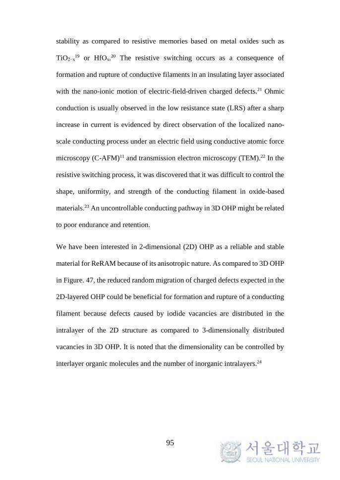
95
stability as compared to resistive memories based on metal oxides such as
TiO2−x19 or HfOx.20 The resistive switching occurs as a consequence of
formation and rupture of conductive filaments in an insulating layer associated
with the nano-ionic motion of electric-field-driven charged defects.21 Ohmic
conduction is usually observed in the low resistance state (LRS) after a sharp
increase in current is evidenced by direct observation of the localized nano-
scale conducting process under an electric field using conductive atomic force
microscopy (C-AFM)11 and transmission electron microscopy (TEM).22 In the
resistive switching process, it was discovered that it was difficult to control the
shape, uniformity, and strength of the conducting filament in oxide-based
materials.23 An uncontrollable conducting pathway in 3D OHP might be related
to poor endurance and retention.
We have been interested in 2-dimensional (2D) OHP as a reliable and stable
material for ReRAM because of its anisotropic nature. As compared to 3D OHP
in Figure. 47, the reduced random migration of charged defects expected in the
2D-layered OHP could be beneficial for formation and rupture of a conducting
filament because defects caused by iodide vacancies are distributed in the
intralayer of the 2D structure as compared to 3-dimensionally distributed
vacancies in 3D OHP. It is noted that the dimensionality can be controlled by
interlayer organic molecules and the number of inorganic intralayers.24

96
Figure 47 Comparison of crystalline structures of 2D BA2PbI4 and 3D MAPbI3
(BA = C4H9NH3 and MA = CH3NH3). (a, c) Cross-sectional and (b, d) top view
of (a, b) BA2PbI4 and (c, d) MAPbI3.
Here, I report the resistive switching of (C4H9NH3)2(CH3NH3)n−1PbnI3n+1
(C4H9NH3= BA, CH3NH3= A) from n=1 to 3 and n=∞ to study the dependency
of resistive switching on the structural change from 3D OHP (MAPbI3) to 2D
layered OHP (BA2PbI4). The interlayer BA cation has a chain sufficiently long
to separate inorganic intralayers comprising PbI6 octahedra, whereas the small
MA cation can be inserted in PbI6 octahedra to increase 3D characteristics. The
resistive switching property is compared to study the effect of dimensionality
on resistive switching behavior. Consequently, 2D OHP is found to be more
reliable and stable in the switching process than quasi 2D and 3D OHPs. I also

97
demonstrate the uniformity of the resistive switching properties using 4 inch
wafer-scale BA2PbI4 thin film.

98
4.2. Experimental Procedures
Synthesis: C4H9NH3I (butylammonium iodide, BAI) was synthesized by
reacting 10ml of C4H9NH2 (Aldrich, 99%) with 20 ml of HI (Aldrich, 57 wt %
in H2O). The C4H9NH2 solution was placed in a round-bottom flask with
magnetic stirring where a HI solution was added dropwise. The reaction
proceeded in an ice bath for 2 h. The white precipitate was collected by
evaporation sing a rotary evaporator at 60 oC. The collected white precipitate
was washed with diethyl ether three times. Finally it filtered and dried for 24 h
in vacuum oven at 60 oC. CH3NH3I (methylammonium iodide, MAI) was
synthesized by reacting 30 ml of CH3NH2 (TCI, 40 wt % in methanol) with 40
ml of HI (Aldrich, 57 st % in H2O). The following steps were same as that of
butylammonium iodide as demonstrated.
Fabrication: The silicon wafer coated by 100 nm of Pt was cleaned by
ultrasonication in detergent, ethanol, acetone and ethanol bath for each 15 min.
It was treated with UV-ozone for 15 min before spin-coating of the perovskite
precursor solution. The BA2MAn-1PbnI3n+1 precursor solution (n=1,2,3) was
prepared by dissolving 1 mmol of PbI2 (Alfa Aesar, 99.999%), x mmol (x=2
for n=1, x=1 for n=2, x=0.66 for n=3) of BAI, y mmol (y=0 for n=1, y=0.5 for
n=2, y=0.66 for n=3) of MAI, and 2 mmol of DMSO (Sigma, >99.9%) in 1 ml
of DMF (Sigma-Aldrich, 99.8%). MAPbI3 precursor solution was prepared by
dissolving 1 mmol of PbI2 with 1 mmol of MAI in 1 ml of DMF. The solution
was spin-coated on the Pt-coated Silicon wafer at 4000 rpm for 40 s.
(acceleration = 1200 rpm/s), to which 0.5 ml of chlorobenzene was dropped

99
after 15 s of spinning (after 10 s for MAPbI3). The spin-coated BA2MAn-
1PbnI3n+1 film (n=1,2,3) as annealed at 55 oC for 1 min and at 100 oC for 50 min
while MAPbI3 was annealed at 70 oC for 50 min. Ag (99.99%) was deposited
as electrode using a thermal evaporator at ca. 10-6 torr. The size of silicon wafer
was 1.5 cm∙1.5 cm or 4 inch diameter wafer, however the fabrications were
same but we dropping 1 ml of chlorobenzene on the 4 inch-scale wafer coated
by perovskite film during spin-coating.
Characterization: The surface and cross sectional images were obtained from
field emission scanning electron microscopy(JEOL, JSM7000F) at accelerating
voltage of 1 kV. All electrical characteristics were measured by using Keithley
4200 in the vacuum probe station at ca. 10-2 torr. The I-V characteristics was
measured by direct voltage current sweeping mode in various temperature and
the resistive switching cycling was measured by direct current voltage pulses
(10 ms of pulse width). X-ray diffraction patterns were obtained using a Rigaku
DMAX-2200PC X-ray diffractometer equipped with a graphite
monochromator (λ = 1.5418 Å). The datasets were collected in the 2θ range of
3–65° with a step size of 0.02°. The lattice parameters were refined using the
UnitCell program38. The a and b lattice parameters for the (BA)2PbI4 sample
were taken from the literature39 because the XRD pattern of (BA)2PbI4 film
prepared in this work showed only (00l) reflections.

100
4.3. Results and Discussion
A schematic of the device’s structure is displayed in Figure. 48a, which shows
that the device is composed of a Pt bottom electrode (BE), an OHP film, and an
Ag top electrode (TE). The OHP film was spin-coated onto the Pt-coated
substrate. The 150 nm-thick Ag top electrodes were formed on the surface of
the OHP film by thermal evaporation, where a dot-patterned shadow mask with
a diameter of 100μm was used. OHP thin films with different dimensionalities
were prepared: 2D BA2PbI4 (n= 1), quasi 2D films of BA2MAPb2I7 (n= 2),
BA2MA2Pb3I10 (n= 3), and 3D MAPbI3 (n=∞). Figure. 48b shows a cross-
sectional scanning electron microscopy (SEM) image of a uniform BA2PbI4
film that was deposited by a one-step solution.
Figure 48 (a) Schematic device structure of Ag/BA2MAn-
1PbnI3n+1/Pt/Ti/SiO2/Si. (b) SEM images for thin film BA2PbI4 on the silicon
substrate coated by 100 nm of Pt.
Pinhole-free thin films for all the studied compositions were confirmed to be
pinhole free (Figure. 49).
101
Figure 49 Cross-sectional scanning electron microscopy images for (a)
BA2PbI4, (b) BA2MAPb2I7, (c) BA2MA2Pb3I10 and (d) MAPbI3. (e) Plane-view
scanning electron microscopy image for BA2PbI4. The OHP thin films formed
on the Pt coated silicon wafer.
According to the comparative study of the observed and calculated X-ray
diffraction (XRD) patterns, all the measured XRD patterns are consistent with
both a previous report24 and the calculated XRD patterns (Figure. 50a–d). For
BA2PbI4, (00l) reflections are exclusively developed, which is indicative of the
preferred orientation along the 2D perovskite slab.24 For BA2MAPb2I7 and
BA2MA2Pb3I10, the predominant (0k0) reflections are also indicative of
anisotropic growth of these phases on the substrate. The (0k0) planes for n=2–

102
4 in (BA)2(MA)n−1PbnI3n+1 are parallel to the perovskite slabs, and they
correspond to the (00l) reflection for n=1.24
Figure 50 XRD peaks reveals the perovskite formation in (a) BA2PbI4, (b)
BA2MAPb2I7, (c) BA2MA2Pb3I10 and (d) MAPbI3.
Figure. 51a–d show the I–V characteristics measured under a direct current (DC)
voltage sweep. Regardless of the dimensionality of the materials, all the OHPs
show bipolar resistive switching behavior. The high resistance state (HRS) is
changed to a low resistance state (LRS) at a certain positive bias with an abrupt
increase in current (SET process). The devices maintain LRSs beyond the SET
voltages, and the abrupt SET process and high ON/OFF ratios clearly suggest
the formation of conducting filaments. When negative bias is applied to the

103
devices, LRSs undergo complete transformation into HRSs (RESET process),
supporting the disruption of the conducting pathways. The compliance current
was 10−2 A and 10−1 A for the SET and RESET processes, respectively. It is
noted here that the SET voltage decreases as the dimensionality changes from
3D to 2D. We also investigated the initial forming process.
Figure 51 I-V characteristics of (a) BA2PbI4, (b) BA2MAPb2I7, (c)
BA2MA2Pb3I10, (d) MAPbI3.
In Figure. 52, I–V curves show little difference in switching voltage and process
between forming and the SET process, which indicates that 2D-layered OHP
and quasi-2D OHP enable the electroforming-free process.
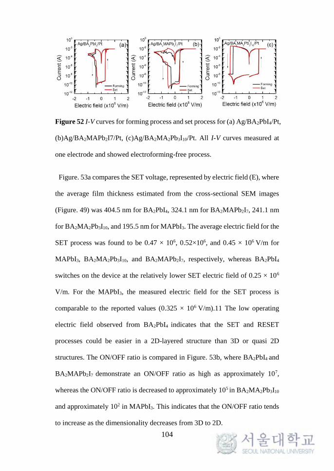
104
Figure 52 I-V curves for forming process and set process for (a) Ag/BA2PbI4/Pt,
(b)Ag/BA2MAPb2I7/Pt, (c)Ag/BA2MA2Pb3I10/Pt. All I-V curves measured at
one electrode and showed electroforming-free process.
Figure. 53a compares the SET voltage, represented by electric field (E), where
the average film thickness estimated from the cross-sectional SEM images
(Figure. 49) was 404.5 nm for BA2PbI4, 324.1 nm for BA2MAPb2I7, 241.1 nm
for BA2MA2Pb3I10, and 195.5 nm for MAPbI3. The average electric field for the
SET process was found to be 0.47 × 10⁶, 0.52×10⁶, and 0.45 × 10⁶ V/m for
MAPbI3, BA2MA2Pb3I10, and BA2MAPb2I7, respectively, whereas BA2PbI4
switches on the device at the relatively lower SET electric field of 0.25 × 10⁶
V/m. For the MAPbI3, the measured electric field for the SET process is
comparable to the reported values (0.325 × 10⁶ V/m).11 The low operating
electric field observed from BA2PbI4 indicates that the SET and RESET
processes could be easier in a 2D-layered structure than 3D or quasi 2D
structures. The ON/OFF ratio is compared in Figure. 53b, where BA2PbI4 and
BA2MAPb2I7 demonstrate an ON/OFF ratio as high as approximately 107,
whereas the ON/OFF ratio is decreased to approximately 105 in BA2MA2Pb3I10
and approximately 102 in MAPbI3. This indicates that the ON/OFF ratio tends
to increase as the dimensionality decreases from 3D to 2D.

105
Figure 53 (a) The electric field for SET process was compared, the lowest
electric field was observed in BA2PbI4. (b) the on/off ratio each material
(Reading voltage was 0.02 V).
To understand the origin of the resistive switching behavior, we plot
logarithmic I–V characteristics of the devices (Figure. 54a–c). Because MAPbI3
is found to be highly sensitive to environmental conditions such as humidity
and oxygen and thereby it exhibits relatively unstable resistive switching
behavior, the switching performance is compared for BA2PbI4, BA2MAPb2I7,
and BA2MA2Pb3I10. In Figure. 54a–c, the LRS is fitted with slope = 1 for all the
samples, which indicates that a conducting filament is formed during the SET
process.28, 29 However, voltage-independent current is exhibited at the HRS,
which is indicative of non-flow of internal electric charges. This result supports
the tenet that the conduction path or underlying mechanism is similar regardless
of the structural dimensionality. The current at the HRS decreases from

106
approximately 10−8 to 10−10 and to 10−11 A as the dimensionality is reduced from
quasi 2D (n= 3 and n=2) to 2D (n= 1). Thus, the increased ON/OFF ratio in 2D
BA2PbI4 is attributed to the significant decrease in the HRS current rather than
a slight change in the LRS current.
Figure 54 Fitted logarithmic I-V characteristics of (a) BA2PbI4, (b)
BA2MA1Pb2I7, (c) BA2MA2Pb3I10.
It was reported that change in dimensionality from 3D MAPbI3 to 2D BA2PbI4
enlarged the bandgap along with changes in valence band maximum and
conduction band minimum,24 which might lead to the different Schottky barrier
heights at the interface of both of the TE Ag and the BE Pt. We calculated the
Schottky barrier heights from the difference between the work function of the
metal electrode and the Fermi level of perovskite (assuming that it is an intrinsic
semiconductor) and found that BA2PbI4 shows the highest barrier at both sides
of the interfaces because of its wider bandgap (Figure. 55). The increase in
barrier height as the dimensionality shifts from 3D to 2D is likely to decrease
the density of the injected carrier from electrode to perovskite, which can
explain the decrease in the HRS current traveling from quasi 2D to 2D, as
observed in Figure. 54a–c.

107
Figure 55 (a) Energy band diagram and (b) Schottky barrier heights at each
metal electrode interface calculated by difference between the Fermi level of
(BA)2(MA)n-1PbnI3n+1 and work function of metal.
We examined the effect of temperature on the electrical characteristics of the
HRS over temperatures ranging from 150 K to 360 K to study further
differences in OFF current at the HRS depending upon dimensionality. In
Figure. 54a–c, resistance at the HRS (Roff) is decreased as the temperature
increases, which is indicative of semiconductor-like behavior. To understand
the temperature-dependent semiconducting behavior of our perovskite samples,
an Arrhenius plot of the HRS current (Ioff) as a function of inverse temperature
was created, which is displayed in the insets of Figure. 54a–c. The electrical
thermal activation energy (Ea) is estimated using equation (1),
ln Ioff = ln I0 −Ea
kT⁄
Where Ioff is the HRS current, I0 is the constant, k is the Boltzmann constant,
and T is the absolute temperature.30 Two distinct Ea values are obtained from
the plots for each sample. In the low temperature region, Ea= 0.047, 0.053, and

108
0.085 eV are estimated for BA2MA2Pb3I10, BA2MA1Pb2I7, and BA2PbI4,
respectively, while a larger Ea of 0.185, 0.190, and 0.583 eV is evaluated for
higher temperatures. This indicates that all the samples have low Ea values
below room temperature but show high Ea values near and above room
temperature. In addition, Ea is increased upon reducing the dimensionality from
quasi 2D to 2D. Ea is related to the donor level (trap state) at the conduction
band, and deeper trap states tend to increase Ea at the HRS and thereby decrease
the OFF current.
Figure 56 Temperature dependent resistance of (a) BA2PbI4, (b) BA2MA1Pb2I7,
(c) BA2MA2Pb3I10. The decreased resistance as temperature increased showed
the typical semiconductor property. In insert figure, two distinguish slope was
determined from In(Ioff)-1/kT plot. It result as two different dominant
conducting mechanism, and highest thermal electronic activation energy was
observed in BA2PbI4 in range of T>300 K.
When considering that the metallic filament is broken in the HRS, the small
current can be explained by thermally excited electrons hopping via the shallow
trap states at high temperatures.31 Ea is thus related to the donor level (trap state)
at the conduction band, and deeper trap states tend to increase Ea at the HRS
and thereby decrease the OFF current. The increase in Ea at high temperatures
109
as the dimensionality reduces from quasi 2D to 2D is ascribed to the deeper trap
states associated with the larger band gap and higher conduction band minimum.
Therefore, higher Schottky barrier heights and Ea are responsible for the smaller
OFF current and higher ON/OFF ratio for 2D BA2PbI4.
Regarding the filament formation mechanism in BA2PbI4, it is unclear, but
iodide migration (or iodide vacancy) is assumed to be dominantly involved
such as that in MAPbI3, as evidenced by X-ray photoelectron spectroscopy
(XPS) study.32 Because both mechanisms of the Ag redox reaction and vacancy
migration can be possible when using an Ag electrode, it is interesting to
investigate whether or not switching at different electrodes occurs. However,
there is no resistive switching response in the Au/BA2PbI4/Pt device even under
an electric field that is 3 times higher compared to Ag/BA2PbI4/Pt (Figure. 57),
which indicates that electrochemical metallization (ECM) by Ag redox reaction
could be dominant in 2D OHP. Nevertheless, it is uncertain whether ECM is
involved because of the lower electric field for the SET (<106 V/m) that exists
as compared to the high electric field (>107 V/m) required for ECM. Further
studies are required to clarify the filament formation mechanism that occurs
with 2D OHP.

110
Figure 57 I-V curve of Au/BA2PbI4/Pt device. The electric field was applied
from positive sweeping to negative sweeping.
Device reliability was determined by the stability and number of switching
cycles. Figure. 58 shows the endurance characteristics for
BA2PbI4 ,BA2MA1Pb2I7, and BA2MA2Pb3I10 A direct current (DC) pulse was
applied with magnitude of 0.5 V for the SET process and −0.6 V for the RESET
process, where the pulse width was 10 ms during more than 250 cycles. It is
noted that perfect resistive switching is realized for Ag/BA2PbI4/Pt for 250
cycles, while quasi 2D perovskites show relatively unstable switching behavior
as the number of cycles increases primarily because of the instability of the
HRS. This indicates that the RESET process is critical to determine the
reliability of devices rather than the SET process. The resistive switching
behavior was reported to be closely related to the shape, uniformity, and
dimension of the conducting filament as well as the defect sites caused by the
crystallographic structure.23

111
Figure 58 Endurance characteristics of Ag/BA2MAn-1PbnI3n+1/Pt, (a) BA2PbI4,
(b) BA2MA1Pb2I7, (c) BA2MA2Pb3I10. SET voltage was 0.5 V and RESET
voltage was -0.6 V. (The pulse width was 10 ms). Reading voltage was + 0.02
V/- 0.02 V.
Two types of conducting filaments in bipolar switching memory devices were
observed by TEM,22,33 SEM,34 and C-AFM35 – a bulky shape22,35 and a
dendrite-like (multiple) shape.33,34 It is expected that the conducting filament
is difficult to completely annihilate under the RESET process. The conducting
filament is expected to be broken for the rupture process in the case of the bulky
shape, and the partially remaining filaments are responsible for the resistance
at the HRS. However, after the rupture process, additional residual filaments
are expected due to multiple filaments in the dendrite-like shape, which can
decrease the resistance at the HRS. Because we observed insulating
characteristics at the HRS and a higher ON/OFF ratio approaching the 2D
structure, it is likely that the bulky filament shape has formed in our 2D system.
A more stable HRS for 2D than quasi 2D in Figure. 58 indicates that residual
filaments at the HRS are formed with less frequency for 2D than for quasi 2D.
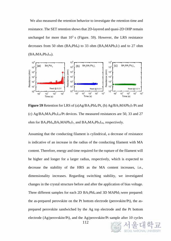
112
We also measured the retention behavior to investigate the retention time and
resistance. The SET retention shows that 2D-layered and quasi-2D OHP remain
unchanged for more than 103 s (Figure. 59). However, the LRS resistance
decreases from 50 ohm (BA2PbI4) to 33 ohm (BA2MAPb2I7) and to 27 ohm
(BA2MA2Pb3I10).
Figure 59 Retention for LRS of (a)Ag/BA2PbI4/Pt, (b) Ag/BA2MAPb2I7/Pt and
(c) Ag/BA2MA2Pb3I10/Pt devices. The measured resistances are 50, 33 and 27
ohm for BA2PbI4,BA2MAPb2I7, and BA2MA2Pb3I10, respectively.
Assuming that the conducting filament is cylindrical, a decrease of resistance
is indicative of an increase in the radius of the conducting filament with MA
content. Therefore, energy and time required for the rupture of the filament will
be higher and longer for a larger radius, respectively, which is expected to
decrease the stability of the HRS as the MA content increases, i.e.,
dimensionality increases. Regarding switching stability, we investigated
changes in the crystal structure before and after the application of bias voltage.
Three different samples for each 2D BA2PbI4 and 3D MAPbI3 were prepared:
the as-prepared perovskite on the Pt bottom electrode (perovskite/Pt), the as-
prepared perovskite sandwiched by the Ag top electrode and the Pt bottom
electrode (Ag/perovskite/Pt), and the Ag/perovskite/Pt sample after 10 cycles

113
of voltage sweeping (one cycle of voltage sweeping consists of: 0.5 V → 0 V→
−0.5 V → 0 V), together with a thin film consisting of a mixture of AgI and
perovskite with 0.8 mmol of AgI with respect to 1 mol of perovskite (mixture
perovskite/Pt) for comparison. Figure. 60 shows the XRD patterns. The cell
volume was calculated from the XRD data to compare the structural changes
during voltage sweeping (Table 3). An unknown peak at approximately 8.5°
was detected after Ag deposition in BA2PbI4 before and after voltage sweeping
(Figure. 60a), while no noticeable unknown peaks were found in MAPbI3
(Figure. 60b). This unknown peak is also observed from the mixture of AgI and
BA2PbI4 but not from the mixture with MAPbI3. This indicates that AgI exists
after deposition of the Ag TE and after voltage sweeping for BA2PbI4. AgI
peaks at approximately 22°, and 24° is less pronounced for both the as-
deposited Ag electrode and the mixture, which is pronounced after voltage
sweeping. For MAPbI3, AgI is not observed; instead, metallic Ag is detected
after Ag deposition and voltage sweeping. From the evolution of XRD, it
cannot be ruled out that migration of Ag+ ion may create a conducting path in
2D BA2PbI4.

114
Figure 60 XRD patterns of four different samples for (a) BA2PbI4 and (b)
MAPbI3, where (1) represents the as-prepared perovskite on Pt electrode
(Perovskite/Pt), (2) the as-prepared perovskite with Ag electrode
(Ag/perovskite/Pt), (3) the sample after 10 cycles of voltage sweeping (bias
aged Ag/perovskite/Pt) and (4) a thin film of mixture of AgI and perovskite
with 0.8 mmol of AgI with respect to 1 mol of perovskite (mixture
perovskite/Pt). The area of Ag was 0.09 cm2 with the thickness of 150 nm. The
voltage sweeping cycle was 0.5 V →0 V →-0.5V→0 V. The perovskite phase
is marked with orange circles. A indicates metallic Ag, # denotes AgI and S
corresponds to peak from silicon wafer.* denotes unknown peak.

115
Sample a (Å ) b (Å ) c (Å ) V (Å 3)
MAPbI3
Bare 8.8528(7) 12.563(3) 984.6(2)
Ag 8.8518(7) 12.565(3) 984.6(2)
Ag_V 8.8559(7) 12.590(3) 987.4(2)
AgI_0.8mmol 8.8594(7) 12.575(3) 987.0(2)
BA2PbI4
Bare 8.862 8.862 27.509(1) 2116.6(4)
Ag 8.862 8.862 27.505(1) 2116.2(4)
Ag_V 8.862 8.862 27.512(1) 2116.8(4)
AgI_0.8mmol 8.862 8.862 27.615(1) 2124.7(4)
Table 3 Lattice parameters and unit cell volumes of the samples
The unit cell volume was calculated to investigate the impact of applied bias on
OHP. The cell volume of MAPbI3 is increased after voltage sweeping, whereas
no significant change in cell volume occurred for BA2PbI4 (Figure. 61). The
improved structural stability of BA2PbI4 under repeated voltage sweeping is in
part responsible for the improved endurance performance.
Figure 61 The unit cell volumes of three different samples mentioned in Figure
56 for (a) BA2PbI4, and (b) MAPbI3 calculated by lattice parameters listed in
Table 3.
To check the feasibility of the 2D OHP for use in a large area scale, we
investigated the resistive switching properties of 4 inch wafer-scale BA2PbI4
thin films. Figure. 62a shows the BA2PbI4 film deposited on a 4 inch wafer,

116
where the wafer-scale film was prepared by the solution process. Five different
areas were chosen, and the resistive switching characteristics were measured.
Figure. 62b–d shows the HRS, LRS, and SET voltage, represented by an
electric field, where little deviation of each property was found.
Figure 62 Reliable resistive switching properties of Ag/BA2PbI4/Pt prepared
on a 4 inch wafer. (a) BA2PbI4 was spin-coated on a 4 inch wafer, and Ag
electrodes were deposited on locations (1) – (5). (b) HRS, (c) LRS, and (d) SET
voltage, represented by electric field (E) on (1) – (5).
The average thickness is found to be 473.4 with deviation of ±30.6 nm (Figure.
63), which is responsible for the small deviation in HRS and LRS. The
measured switching properties of the 4 inch wafer are found to be nearly
comparable to those of the small-sized device.

117
Figure 63 BA2PbI4 film deposited on (a) Si wafer and (b) its thickness
measured from different part designated in (a).
The reliable switching property of the 4 inch large-scale wafer suggests the
feasibility of low-cost and large-area 2D OHP-based resistive memory.
Reliability is further confirmed from 20 electrodes at room temperature (Figure.
64a and b). Bipolar switching is observed at the elevated temperature of 87 °C,
which is probably related to the non-phase transition of 2D perovskite (Figure
64c). Our data strongly suggests that BA2PbI4 is suitable for non-volatile
memory, which should be capable of operating at elevated temperatures in a
high-density electronic circuit.
Figure 64 (a) Comparison of I-V characteristics from 5 repeated sweeps at
room temperature. (b) Distribution of resistances in HRS and LRS was shown
(read at 0.02 V). (c) I-V characteristics measured at 87 oC.

118
4.4. Conclusion
We prepared and studied the resistive switching behavior of BA2MAn−1PbnI3n+1
films for n=1,2,3 and ∞ (2D layered structure for n= 1 and 3D structure for
n=∞). The anisotropic 2D structure exhibited a lower operating voltage, higher
ON/OFF ratio, and more stable endurance without failure during 250 cycles
compared to the quasi 2D and 3D structure. It was confirmed that higher
Schottky barrier heights and Ea were responsible for the smaller HRS current
and higher ON/OFF ratio for 2D BA2PbI4. We obtained for the first time reliable
resistive switching from a 4 inch wafer-scale device based on solution-
processed BA2PbI4. Stable resistive switching behavior was observed even at
the elevated temperature of 87 °C. Our results suggest that 2D perovskite is a
promising material for a resistive memory device.

119
4.5. References
1. Kim, H.-S.; Lee, C.-R.; Im, J.-H.; Lee, K.-B.; Moehl, T.; Marchioro, A.;
Moon, S.-J.; Humphry-Baker, R.; Yum, J.-H.; Moser, J. E.; Grätzel, M.;
Park, N.-G. Sci. Rep. 2012, 2, srep00591.
2. Filip, M. R.; Eperon, G. E.; Snaith, H. J.; Giustino, F. Nat. Commun.
2014, 5, ncomms6757.
3. Eperon, G. E.; Stranks, S. D.; Menelaou, C.; Johnston, M. B.; Herz, L.
M.; Snaith, H. J. Energy Environ. Sci. 2014, 7 (3), 982–988.
4. Gu, C.; Lee, J.-S. ACS Nano 2016, 10 (5), 5413–5418.
5. Shi, D.; Adinolfi, V.; Comin, R.; Yuan, M.; Alarousu, E.; Buin, A.; Chen,
Y.; Hoogland, S.; Rothenberger, A.; Katsiev, K.; Losovyj, Y.; Zhang, X.;
Dowben, P. A.; Mohammed, O. F.; Sargent, E. H.; Bakr, O. M. Science
2015, 347 (6221), 519–522.
6. Stranks, S. D.; Eperon, G. E.; Grancini, G.; Menelaou, C.; Alcocer, M.
J. P.; Leijtens, T.; Herz, L. M.; Petrozza, A.; Snaith, H. J. Science 2013,
342 (6156), 341–344.
7. Miyata, A.; Mitioglu, A.; Plochocka, P.; Portugall, O.; Wang, J. T.-W.;
Stranks, S. D.; Snaith, H. J.; Nicholas, R. J. Nat. Phys. 2015, 11 (7), 582–
587.
8. Yuan, M.; Quan, L. N.; Comin, R.; Walters, G.; Sabatini, R.; Voznyy, O.;
Hoogland, S.; Zhao, Y.; Beauregard, E. M.; Kanjanaboos, P.; Lu, Z.; Kim,
D. H.; Sargent, E. H. Nat. Nanotechnol. 2016, 11 (10), 872–877.
9. Lee, J.-W.; Choi, Y. J.; Yang, J.-M.; Ham, S.; Jeon, S. K.; Lee, J. Y.; Song,
Y.-H.; Ji, E. K.; Yoon, D.-H.; Seo, S.; Shin, H.; Han, G. S.; Jung, H. S.;

120
Kim, D.; Park, N.-G. ACS Nano 2017, 11 (3), 3311–3319.
10. Xing, G.; Mathews, N.; Lim, S. S.; Yantara, N.; Liu, X.; Sabba, D.;
Grätzel, M.; Mhaisalkar, S.; Sum, T. C. Nat. Mater. 2014, 13 (5), 476–
480.
11. Heiss, W.; Brabec, C. Nat. Photonics 2016, 10 (5), 288–289.
12. Chin, X. Y.; Cortecchia, D.; Yin, J.; Bruno, A.; Soci, C. Nat. Commun.
2015, 6, ncomms8383.
13. Xu, W.; Cho, H.; Kim, Y.-H.; Kim, Y.-T.; Wolf, C.; Park, C.-G.; Lee, T.-
W. Adv. Mater. 2016, 28 (28), 5916–5922.
14. Choi, J.; Park, S.; Lee, J.; Hong, K.; Kim, D.-H.; Moon, C. W.; Park, G.
D.; Suh, J.; Hwang, J.; Kim, S. Y.; Jung, H. S.; Park, N.-G.; Han, S.;
Nam, K. T.; Jang, H. W. Adv. Mater. 2016, 28 (31), 6562–6567.
15. Yan, K.; Peng, M.; Yu, X.; Cai, X.; Chen, S.; Hu, H.; Chen, B.; Gao, X.;
Dong, B.; Zou, D. J. Mater. Chem. C 2016, 4 (7), 1375–1381.
16. Hwang, B.; Gu, C.; Lee, D.; Lee, J.-S. Sci. Rep. 2017, 7, srep43794.
17. Liu, D.; Lin, Q.; Zang, Z.; Wang, M.; Wangyang, P.; Tang, X.; Zhou, M.;
Hu, W. ACS Appl. Mater. Interfaces 2017, 9 (7), 6171–6176.
18. Yoo, E.; Lyu, M.; Yun, J.-H.; Kang, C.; Choi, Y.; Wang, L. J. Mater.
Chem. C 2016, 4 (33), 7824–7830.
19. Lee, M.-J.; Lee, C. B.; Lee, D.; Lee, S. R.; Chang, M.; Hur, J. H.; Kim,
Y.-B.; Kim, C.-J.; Seo, D. H.; Seo, S.; Chung, U.-I.; Yoo, I.-K.; Kim, K.
Nat. Mater. 2011, 10 (8), 625–630.
20. Lee, H. Y.; Chen, P. S.; Wu, T. Y.; Chen, Y. S.; Wang, C. C.; Tzeng, P. J.;
Lin, C. H.; Chen, F.; Lien, C. H.; Tsai, M. J. In 2008 IEEE International

121
Electron Devices Meeting; 2008; pp 1–4.
21. Kwon, D.-H.; Kim, K. M.; Jang, J. H.; Jeon, J. M.; Lee, M. H.; Kim, G.
H.; Li, X.-S.; Park, G.-S.; Lee, B.; Han, S.; Kim, M.; Hwang, C. S. Nat.
Nanotechnol. 2010, 5 (2), 148–153.
22. Kim, K. M.; Jeong, D. S.; Hwang, C. S. Nanotechnology 2011, 22 (25),
254002.
23. Cao, D. H.; Stoumpos, C. C.; Farha, O. K.; Hupp, J. T.; Kanatzidis, M.
G. J. Am. Chem. Soc. 2015, 137 (24), 7843–7850.
24. Zhuge, F.; Peng, S.; He, C.; Zhu, X.; Chen, X.; Liu, Y.; Li, R.-W.
Nanotechnology 2011, 22 (27), 275204.
25. Gao, S.; Chen, C.; Zhai, Z.; Liu, H. Y.; Lin, Y. S.; Li, S. Z.; Lu, S. H.;
Wang, G. Y.; Song, C.; Zeng, F.; Pan, F. Appl. Phys. Lett. 2014, 105 (6),
063504.
26. Yang, C.-S.; Shang, D.-S.; Chai, Y.-S.; Yan, L.-Q.; Shen, B.-G.; Sun, Y.
Phys. Chem. Chem. Phys. 2016, 18 (18), 12466–12475.
27. Wang, Z. Q.; Xu, H. Y.; Zhang, L.; Li, X. H.; Ma, J. G.; Zhang, X. T.;
Liu, Y. C. Nanoscale 2013, 5 (10), 4490–4494.
28. Szot, K.; Speier, W.; Bihlmayer, G.; Waser, R. Nat. Mater. 2006, 5 (4),
312–320.
29. Kim, K. M.; Choi, B. J.; Shin, Y. C.; Choi, S.; Hwang, C. S. Appl. Phys.
Lett. 2007, 91 (1), 012907.
30. Jung, K.; Seo, H.; Kim, Y.; Im, H.; Hong, J.; Park, J.-W.; Lee, J.-K. Appl.
Phys. Lett. 2007, 90 (5), 052104.
31. Cao, B.; Cai, W.; Zeng, H. Appl. Phys. Lett. 2006, 88 (16), 161101.

122
32. Hsiung, C.-P.; Liao, H.-W.; Gan, J.-Y.; Wu, T.-B.; Hwang, J.-C.; Chen,
F.; Tsai, M.-J. ACS Nano 2010, 4 (9), 5414–5420.
33. Yang, Y.; Gao, P.; Gaba, S.; Chang, T.; Pan, X.; Lu, W. Nat. Commun.
2012, 3, 1737.
34. Celano, U.; Goux, L.; Belmonte, A.; Opsomer, K.; Franquet, A.; Schulze,
A.; Detavernier, C.; Richard, O.; Bender, H.; Jurczak, M.; Vandervorst,
W. Nano Lett. 2014, 14 (5), 2401–2406.
35. Strachan, J. P.; Pickett, M. D.; Yang, J. J.; Aloni, S.; David Kilcoyne, A.
L.; Medeiros-Ribeiro, G.; Stanley Williams, R. Adv. Mater. 2010, 22
(32), 3573–3577.
36. Wiesmann, H. J.; Zeller, H. R. J. Appl. Phys. 1986, 60 (5), 1770–1773.
37. Chae, S. C.; Lee, J. S.; Kim, S.; Lee, S. B.; Chang, S. H.; Liu, C.; Kahng,
B.; Shin, H.; Kim, D.-W.; Jung, C. U.; Seo, S.; Lee, M.-J.; Noh, T. W.
Adv. Mater. 2008, 20 (6), 1154–1159.
38. Holland, T. J. B.; Redfern, S. a. T. Mineral. Mag. 1997, 61 (1), 65–77.
39. Mitzi, D. B. Chem. Mater. 1996, 8 (3), 791–800.

123
Chapter 5
A Fundamental Approach for extended RS
performance
Quote
Leon O. Chua
“The three basic two-terminal circuit elecments are defined in terms
of a relationship between two of the four fundamental circuit
variables.” (1971)

124
5.1. Introduction
In recent years, several intensive research have been in progress for the
application of halide perovskites (HPs) in microelectronic devices beyond solar
cells,1–3 such as light-emitting diodes,4, 5 photodetectors,6, 7 resistive switching
devices,8–10 thin-film transistors,11–13 and artificial synapses.14, 15 This is
particularly true because HP-based resistive switching memories exhibit low-
operation voltages, reduced power consumption, high on/off ratios, and
remarkable mechanical flexibility.9, 16 These outstanding properties are suitable
for next-generation resistive switching memories. However, the present HP-
based resistive switching memories have critical weaknesses, such as short
endurance and poor air-stability. To overcome these limitations, diverse
solutions have been reported. One strategy is discovering and synthesizing
more stable chemical compositions of HPs. To obtain stable resistive switching
properties, various compositions of HPs have been investigated and reported.17–
19 Another strategy is adopting a passivation layer on HP films, such as
polymethyl methacrylate (PMMA), zinc oxide, and ethylene diamine, so as to
isolate the films from the atmosphere and complement their defects.20–23 The
other strategy is by improving the morphology of the HP films. In this regard,
solvent engineering can be employed. By dripping antisolvents, such as toluene,
benzene, and chlorobenzene, and adding hydroiodic acid solution as an additive
in the precursor solution of HPs, morphologically uniform and high quality HP
films24–27 can be obtained. Nevertheless, these strategies still could not provide
the fundamental solutions to the degradation mechanism in resistive switching
devices.

125
I have been interested in the use of HPs for resistive switching devices because
HP easily changes its composition and crystalline structure by a certain
tolerance factor (t) value.28, 29 The MAPbI3 crystalline structure is a pseudo-
cubic structure under ambient conditions. However, the MA+ cation of MAPbI3
in BX6 octahedral void causes a disordered structure and exhibits hysteresis,
which is an important factor in the resistive switching behavior.30, 31 Hence,
MAPbI3 is weak under ambient conditions because of the volatile MA+ cation.
On the other hand, the RbPbI3 crystalline structure is orthorhombic, which is
extremely stable under ambient conditions because of the less volatile Rb+
cation and can be stabilized as a one-dimensional orthorhombic configuration
in nature.32–35 A stable mixture of HPs was made by mixing stable RbPbI3. The
controlled Ag migration in Rb1-xMAxPbI3 could be beneficial for the resistive
switching behavior because of the control formation and rupture of the
conducting bridge by the non-switchable RbPbI3.
Here, I report the mixture of non-switchable RbPbI3 and switchable MAPbI3
as resistive switching memory to control the growth of the Ag bridge, which
connects between the top and bottom electrodes. With the ultralow operation
electric field and on/off ratio, all solutions processed Rb1-xMAxPbI3 resistive
switching memory shows three times extended endurance than pristine MAPbI3
memories. To provide direct evidence for the resistive switching behavior,
conductive atomic force microscopy (CAFM) and energy-dispersive X-ray
spectroscopy (EDS) mapping were highlighted with a field scanning electron
microscope (FE-SEM) to observe the role of the Ag bridge through the HP films
as an insulator. To enhance air stability, a solution-processed ultrathin PMMA

126
layer coated on a perovskite layer protects the device from water vapor and
oxygen in atmosphere. Our study provides a new strategy to enhance the
endurance of HP-based resistive switching memories for next generation non-
volatile computer storage.

127
5.2. Experimental Procedures
Materials preparation: All materials were used without purification. PbI2
(99.9985%) was purchased from Alfa Aesar (U.S.A.) and CH3NH3I from
Xi'AnP-OLED Co. (China). Expect of two materials and RbI (99.9%) were
purchased from Sigma-Aldrich (U.S.A).
Film formation and MIM cell fabrication: The Pt (100 nm)/Ti (20 nm)-
deposited substrates were prepared by an electron beam evaporator. The Pt/Ti-
coated Si wafer substrates were cleaned by an ultrasonic-bath in acetone,
ethanol, and deionized water, each for 15 min. The prepared mixture perovskite
solution is 55 wt.% CH3NH3I, RbI, PbI2 and DMSO (Sigma-Aldrich, >99.9%),
at 1-x:x:1:1 molar ratio, in N,N-dimethylformamide (Sigma-Aldrich, 99.8%).
The perovskite precursor solution was coated on the Pt/Ti-coated Si wafer
substrate by the adduct method reported by Park et al. The 8.5μL of dissolved
solution was spin-coated on the substrates at 4000 rpm for 20 s and after starting
spin-coating, 0.5 mL of diethyl ether drops (Sigma Aldrich) were provided for
10 s. The spin-coated mixture perovskite films were annealed at 70 °C for 1
min and thereafter at 100 °C for 5 min. Then, as it cooled to room temperature,
20 μL of PMMA solution was deposited by spin-coating at 4000 rpm for 30 s.
The solution consisted of 2 mg PMMA (Sigma Aldrich) in 1 mL of
chlorobenzene (Sigma Aldrich, 99.8%). The device was fabricated using a
thermal evaporator of 100-nm thick Ag through the shadow mask at a pressure
of 3×10⁻⁶ Torr.
Device characterization: The surface and cross-sectional images were
obtained by FE-SEM (JSM-7600F, JEOL). The crystalline structures were

128
detected by X-ray diffractometer (D8 advance, Bruker) with Cu Kα radiation
(λ = 1.54056 Å). The XRD data was recorded in the range of 5–60° of the 2
theta range with a scan speed of 6° min−1. Samples of TEM were prepared by
FIB (JIB-4601F, JEOL). Then, the distribution of elements on the mixture
perovskite films was detected by TEM/EDS (JEM ARM 200F, JEOL). The I-
V characteristics of the device (DC voltage sweeping mode) and resistive
switching by alternating voltage pulse were achieved using an Agilent 4156C
semiconductor analyzer under a vacuum of 6×10⁻² Torr. To observe the
topography and resistance change of the Rb1-xMAxPbI3 films, the films
deposited on a Ag/Ti/SiO2/Si substrate were measured using an AFM (Park
systems XE100).
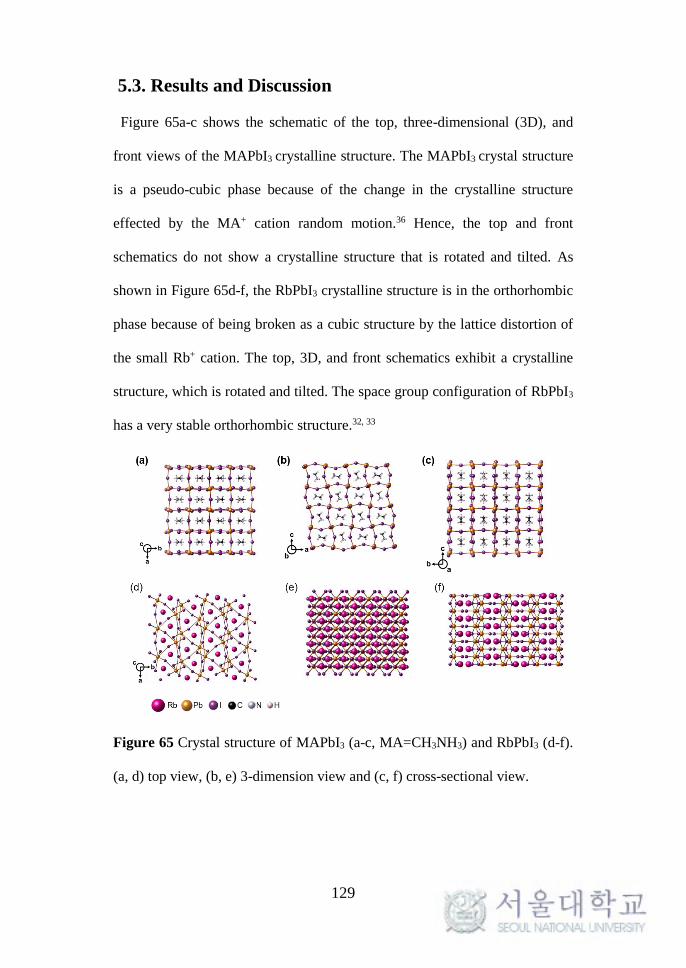
129
5.3. Results and Discussion
Figure 65a-c shows the schematic of the top, three-dimensional (3D), and
front views of the MAPbI3 crystalline structure. The MAPbI3 crystal structure
is a pseudo-cubic phase because of the change in the crystalline structure
effected by the MA+ cation random motion.36 Hence, the top and front
schematics do not show a crystalline structure that is rotated and tilted. As
shown in Figure 65d-f, the RbPbI3 crystalline structure is in the orthorhombic
phase because of being broken as a cubic structure by the lattice distortion of
the small Rb+ cation. The top, 3D, and front schematics exhibit a crystalline
structure, which is rotated and tilted. The space group configuration of RbPbI3
has a very stable orthorhombic structure.32, 33
Figure 65 Crystal structure of MAPbI3 (a-c, MA=CH3NH3) and RbPbI3 (d-f).
(a, d) top view, (b, e) 3-dimension view and (c, f) cross-sectional view.

130
Figure 66 shows the X-ray diffraction (XRD) patterns of MAPbI3, RbPbI3,
and different RbI concentration because of the formation of Rb1-xMAxPbI3. A
single-phase halide perovskite was confirmed from pristine MAPbI3 (orange
line) and RbPbI3 (magenta line).37, 38 As the concentration of RbI increases, Rb1-
xMAxPbI3 is formed because both MAPbI3 and RbPbI3 XRD patterns were
observed. As the concentration of RbPbI3 increases, the intensity of RbPbI3
XRD pattern increases, whereas the intensity of MAPbI3 XRD pattern
decreases. This is because the MAPbI3 crystalline structure is broken and the
RbPbI3 is formed by the lattice distortion of the three-dimensional network of
BX6 distortion as a result of the Rb+ ion being smaller than the MA+ ion.

131
Figure 66 X-ray diffraction pattern of the Rb(1-x)MAxPbI3/Pt substrates.
(Orange line - MAPbI3, Red line – Rb0.31MA0.69PbI3, Blue line -
Rb0.52MA0.48PbI3, Green line - Rb0.71MA0.29PbI3 and Magenta line - RbPbI3)
To investigate the entire distribution of RbPbI3 and MAPbI3 crystalline
structure, we conducted an energy-dispersive X-ray spectroscopy mapping of
the rubidium and lead atoms using a scanning-transmission electron
microscope (STEM) on a vertical PMMA/Rb1-xMAxPbI3/Pt/Ti/SiO2/Si sample,
made by focused ion beam (FIB) milling. The aforementioned is conducted
because only rubidium atoms are detected from RbPbI3, whereas lead atoms are
detected from both RbPbI3 and MAPbI3. The EDS mapping shows the
distribution of RbPbI3 in MAPbI3 by the distribution of rubidium atoms, which
are related to lead atoms. Figure 67a–e shows the cross-sectional view of STEM

132
images of PMMA/Rb1-xMAxPbI3/Pt/Ti/SiO2/Si devices and their EDS mapping
for rubidium and lead atoms. In the STEM dark field image of pristine MAPbI3,
grain boundaries were observed. The distribution of rubidium and lead atoms
is counted in MAPbI3. However, the pristine MAPbI3 does not involve
rubidium atoms. Accordingly, rubidium atoms in the MAPbI3 are counted by
means of characteristic X-ray that is called hard X-ray. The hard X-ray
generates from aperture, holder, lens, vacuum chamber and specimen.
Backscattering of X-ray phonons occurs first from specimen then from bulk.
These scattering X-ray phonons can generates continuous and characteristic X-
ray.39 Therefore, small amounts of rubidium atoms, confirmed to exist only in
MAPbI3, were ignored by hard X-ray (Figure 67a). For pure RbPbI3 STEM dark
field image, the grain boundary was not detected. On the other hand, rubidium
and lead atoms were detected throughout the thin films. Where the amount of
rubidium atoms is close to the amount of lead atoms, it was confirmed to
synthesize the pristine RbPbI3 (Figure 67e). To increase RbPbI3 concentration,
grain boundaries were reduced with the mixture of MAPbI3 and RbPbI3. As the
concentration of RbI increases, the rubidium atoms become uniform in
distribution and their concentration increases. Hence, a uniform distribution
and an increased concentration of RbPbI3 can be observed. This suggests that
the concentration of RbPbI3 is inversely proportional to the grain boundaries in
the Rb1-xMAxPbI3 film.
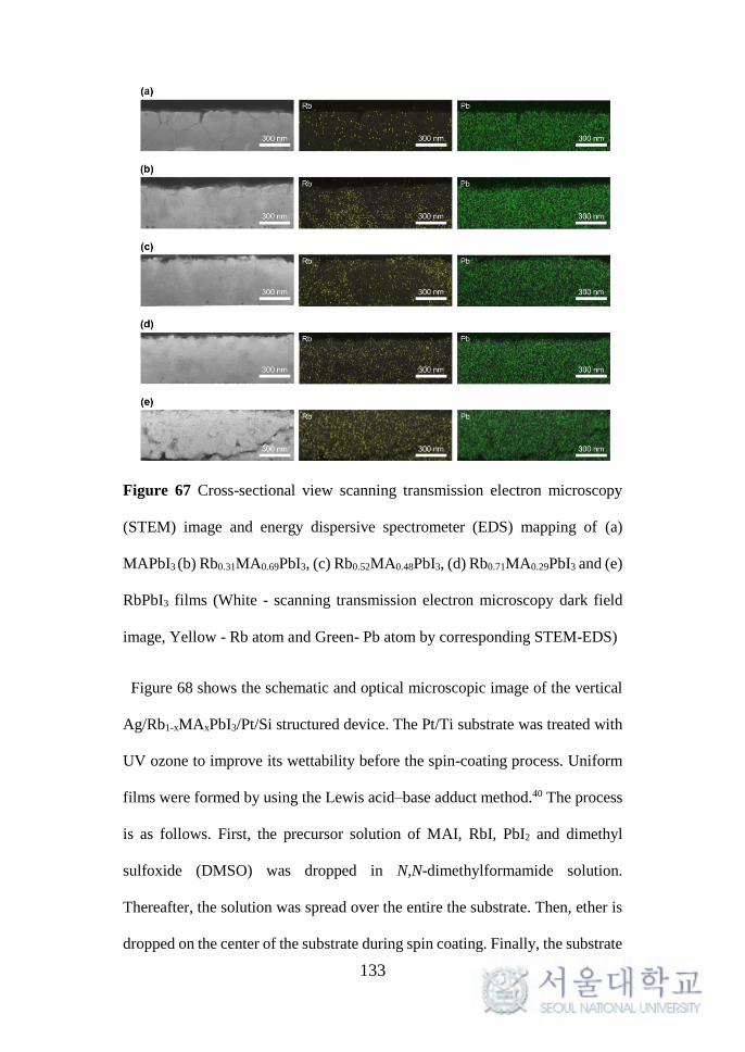
133
Figure 67 Cross-sectional view scanning transmission electron microscopy
(STEM) image and energy dispersive spectrometer (EDS) mapping of (a)
MAPbI3 (b) Rb0.31MA0.69PbI3, (c) Rb0.52MA0.48PbI3, (d) Rb0.71MA0.29PbI3 and (e)
RbPbI3 films (White - scanning transmission electron microscopy dark field
image, Yellow - Rb atom and Green- Pb atom by corresponding STEM-EDS)
Figure 68 shows the schematic and optical microscopic image of the vertical
Ag/Rb1-xMAxPbI3/Pt/Si structured device. The Pt/Ti substrate was treated with
UV ozone to improve its wettability before the spin-coating process. Uniform
films were formed by using the Lewis acid–base adduct method.40 The process
is as follows. First, the precursor solution of MAI, RbI, PbI2 and dimethyl
sulfoxide (DMSO) was dropped in N,N-dimethylformamide solution.
Thereafter, the solution was spread over the entire the substrate. Then, ether is
dropped on the center of the substrate during spin coating. Finally, the substrate

134
is annealed to remove the solvent. To fabricate the vertical MIM structure
device, the Ag top electrodes are deposited using a thermal evaporator and a
100 × 100 μm2 dot patterned shadow mask.
Figure 68 Schematic (left) and optical microscopic image (right) of
Ag/PMMA/Rb1-xMAxPbI3/Pt devices.
From typical cross-sectional SEM images, pristine polycrystalline MAPbI3
and Rb1-xMAxPbI3 layers were observed to be deposited on the Pt/Ti deposited
Si substrates. The 500-nm thick pristine MAPbI3 and Rb1-xMAxPbI3 films were
uniformly deposited and pin-hole free with antisolvent dripping (Figure 69).
For a comparison of resistive switching properties in pristine MAPbI3 and Rb1-
xMAxPbI3, the thickness of all HP films were fixed for the application
equivalent electric fields.

135
Figure 69 Cross-sectional view SEM image of the Ag/PMMA/Rb1-
xMAxPbI3/Pt devices. (a) MAPbI3 (b) Rb0.31MA0.69PbI3, (c) Rb0.52MA0.48PbI3, (d)
Rb0.71MA0.29PbI3 and (e) RbPbI3.
As shown in the plane-view SEM images, the average grain sizes of the HP
films, which are pristine MAPbI3 and RbPbI3 concentrations of 30, 50, and 70%,
are 150, 126, 85, and 70 nm, respectively (Figure 70). The average grain size
of HP films tends to be reduced as the concentration of RbPbI3 is increased.
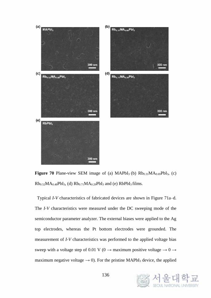
136
Figure 70 Plane-view SEM image of (a) MAPbI3 (b) Rb0.31MA0.69PbI3, (c)
Rb0.52MA0.48PbI3, (d) Rb0.71MA0.29PbI3 and (e) RbPbI3 films.
Typical I-V characteristics of fabricated devices are shown in Figure 71a–d.
The I-V characteristics were measured under the DC sweeping mode of the
semiconductor parameter analyzer. The external biases were applied to the Ag
top electrodes, whereas the Pt bottom electrodes were grounded. The
measurement of I-V characteristics was performed to the applied voltage bias
sweep with a voltage step of 0.01 V (0 → maximum positive voltage → 0 →
maximum negative voltage → 0). For the pristine MAPbI3 device, the applied

137
maximum positive and negative voltages were +0.3 and −0.3 V. Similarly, the
applied maximum positive and negative voltages for RbPbI3 with
concentrations of 31, 52, 71, and 100% (pristine RbPbI3) mixed devices were
±1, ±1, ±1.5, and ±2 V, respectively. In the initial DC sweeping, Rb1-xMAxPbI3
devices showed an electroforming process. Present studies have reported that
HP-based resistive switching devices are electroforming-free regardless of the
switching mechanism.8–10 However, our Rb1-xMAxPbI3-based resistive
switching devices exhibited electroforming process, which is analogous to
general resistive switching devices.41, 42 The voltage for the electroforming
process is also proportional to the concentration of RbPbI3. The electroforming
voltage for RbPbI3 with concentrations of 30, 50, and 70% was +0.6, +1.2, and
+1.35 V, respectively. After the electroforming process, all devices, except the
pristine RbPbI3-based device, showed general resistive switching behaviors.
Initially, the devices maintained high resistance states (HRS, ~10−9 A).
Thereafter, the current levels sharply increased and became low resistance
states (LRS, ~10−3 A), where the applied bias is approximately +0.25 V. After
applying a negative bias of approximately −0.12 V, the devices abruptly turned
to an HRS. All of the devices exhibited general bipolar switching without the
pristine RbPbI3 device. These I-V characteristics suggest that the conducting
paths through HP films are localized by the conducting bridge. However, the
pristine RbPbI3 device did not show resistive switching behavior even though
high voltage (~2 V) was applied. After the electroforming process, the Rb1-
xMAxPbI3 resistive switching devices exhibited a SET voltage of approximately
+0.25 V, except for the pristine RbPbI3 device.

138
Figure 71 Typical current−voltage (I−V) characteristics of Ag/PMMA/RbPbI3
mixed MAPbI3/Pt devices. (a) MAPbI3 and RbPbI3, (b) Rb0.31MA0.69PbI3, (c)
Rb0.52MA0.48PbI3, and (d) Rb0.71MA0.29PbI3.
As described in Figure 72a–d, the endurance of the resistive switching with
voltage pulses (alternating current biases) was measured without the pristine
RbPbI3-based device. The switching voltage for the SET process is slightly
different. The pristine MAPbI3 and 30% of the RbPbI3 mixed with MAPbI3
devices were operable with a SET voltage of +0.3 V (SET) and −1 V (RESET).
On the other hand, 50 and 70% of the RbPbI3 mixed devices were switchable
with a higher SET voltage of +0.5 V. The RESET voltage was equivalent for
all devices. Because of the limitation of the semiconductor parameter analyzer,
the switching speed was fixed to 640 μs. The endurance of the pristine MAPbI3

139
device was 300 cycles (Figure 72a). However, Rb1-xMAxPbI3 devices exhibited
extended endurance. This tendency becomes more pronounced as the
concentration of RbPbI3 is increased. The devices with RbPbI3 concentrations
of 31, 52, and 71% showed endurance of 670, 820, and 970 cycles, respectively
(Figure 72b–d). This result suggests that the non-switchable RbPbI3 contributes
to the stable formation and rupture of a conducting bridge between the top and
bottom electrodes.
Figure 72 Reversible resistive switching behavior measured with the voltage
pulses. Pulse width is fixed to 640 μs. (a) MAPbI3, (b) Rb0.31MA0.69PbI3, (c)
Rb0.52MA0.48PbI3, and (d) Rb0.71MA0.29PbI3.
The retention characteristics of both pristine MAPbI3 and Rb1-xMAxPbI3
devices were up to 12 000 s in HRS (Figure S3). In LRS, the retention
characteristics of the pristine MAPbI3 devices were up to 5200 s, and Rb1-

140
xMAxPbI3 devices exhibited from 8000–10000 s, irrespective of the
concentration of RbPbI3.
Figure 73 Retention characteristics of the Ag/PMMA/Rb1-xMAxPbI3/Pt devices.
(a) MAPbI3 (b) Rb0.31MA0.69PbI3, (c) Rb0.52MA0.48PbI3, and (d) Rb0.71MA0.29PbI3
In order to check the long-term stability, we measured I-V characteristics of
Ag/PMMA/Rb1-xMAxPbI3/Pt devices. The devices were stored in ambient
condition I-V characteristics of the devices were conducted every day. Since
PMMA layer (~30 nm) for passivation protected Rb1-xMAxPbI3 films from H2O
and O2 in ambient condition, the devices exhibited general bipolar resistive
switching behavior for 8 days (Figure 74).
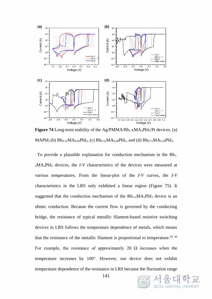
141
Figure 74 Long-term stability of the Ag/PMMA/Rb1-xMAxPbI3/Pt devices. (a)
MAPbI3 (b) Rb0.31MA0.69PbI3, (c) Rb0.52MA0.48PbI3, and (d) Rb0.71MA0.29PbI3.
To provide a plausible explanation for conduction mechanism in the Rb1-
xMAxPbI3 devices, the I-V characteristics of the devices were measured at
various temperatures. From the linear-plot of the I-V curves, the I-V
characteristics in the LRS only exhibited a linear region (Figure 75). It
suggested that the conduction mechanism of the Rb1-xMAxPbI3 device is an
ohmic conduction. Because the current flow is governed by the conducting
bridge, the resistance of typical metallic filament-based resistive switching
devices in LRS follows the temperature dependence of metals, which means
that the resistance of the metallic filament is proportional to temperature.43, 44
For example, the resistance of approximately 20 Ω increases when the
temperature increases by 100°. However, our device does not exhibit
temperature dependence of the resistance in LRS because the fluctuation range

142
of the resistance in LRS is greater than the increase in resistance when
temperature increases.16
Figure 75 Linear I−V characteristics of the Ag/PMMA/Rb1-xMAxPbI3/Pt
devices in low resistance state.
In HRS, the I-V characteristics of the Rb1-xMAxPbI3 device showed both linear
and non-linear regions (Figure 76a). Generally, previous studies of halide
perovskite-based resistive switching devices described that the conduction is
governed by the space charge limited conduction (SCLC) in HRS.8, 9 However,
SCLC is not appropriate for our device because the slope of the non-linear
region in I-V curves is proportional to the temperature in HRS (Figure 76a and
b). To interpret the conduction behavior in HRS, we fitted the I-V
characteristics and computed the average ion hopping distances (Figure 76b).41,
45 The thermally-assisted ion hopping is governed by the equation,
𝐽 = 𝜎𝑇𝐴𝐻𝐸 = 𝑛𝑐2𝜈𝑇𝐴𝐻𝑎𝑞𝑒exp (Δ𝛨
𝑘𝑇) 𝑠𝑖𝑛ℎ (
𝑞𝑒𝐸𝑎
2𝑘𝑇)
where 𝑛𝑐 is the concentration of the majority carrier, 𝑞𝑒 is the elementary
charge, υ is the frequency factor, and 𝑎 is the ion hopping distance. We aimed
at determining the relationship between the ion hopping distance, 𝑎 , and
temperature, T. With the fitted I-V characteristics, the simplified equation,

143
𝐽 = 𝑁𝑠𝑖𝑛ℎ (𝑞𝑒𝐸𝑎
2𝑘𝑇), 𝑁=𝑛𝑐2𝜈𝑇𝐴𝐻𝑎𝑞𝑒exp(
Δ𝛨
𝑘𝑇)
resulted to the ion hopping distances of 78.31, 93.25, 109.26, 129.45, and
164.43 nm at 208, 238, 268, 298, and 328 K, respectively. The above equation
and I-V characteristics indicate that the ion hopping distance is proportional to
temperature. Therefore, this suggests that the conduction mechanism of the
RbPbI3 mixed MAPbI3 devices is an ohmic conduction in LRS and a thermally
assisted ion hopping mechanism in HRS.
Figure 76 Logarithmic I−V characteristics of the Ag/PMMA/Rb1-xMAxPbI3/Pt
devices in (a) low resistance state and (b) high resistance state.
To investigate the source of the resistive switching behavior in HP films, we
conducted a CAFM measurement of the vertical PMMA/Rb1-
xMAxPbI3/PMMA/Ag/Ti/SiO2/Si structured device. The concentration of
RbPbI3 was 50%. To observe the migration of Ag ions, we used an Ag coated
Si substrate. Because of the electrochemically active Ag bottom electrodes,
ultrathin PMMA layers (~30 nm) were deposited between the Ag bottom
electrodes and HP films to prevent a reaction, resulting in the formation of AgI
layer (Figure 77).46, 47

144
Figure 77 The effect of the PMMA layer to prevent chemical reation between
Ag top eletrodes and halide perovskite films. (a) PMMA coated, and (b) non-
coated MAPbI3 films.
Figure 78 shows topological atomic force microscopy images of 10 × 10 μm2
HP films. The root mean square roughness is 11.475 nm and the average grain
size is approximately 83 nm.
Figure 78 Topological atomic force microscopy (AFM) images of the RbPbI3
mixed MAPbI3 films of 10 × 10 μm2 (left). The roughness is measured by AFM
tips moving along the green and red dotted lines by distance (right).
First, a bias of 0.4 V was applied to the HP films of area 10 × 10 μm2. At a bias
of 0.4 V on the Pt coated tip, the Rb1-xMAxPbI3 film was fully insulating at

145
current levels of 6–8 × 10⁻⁹ A (Figure 79a). Then, we applied a bias of 0.8 V to
an area of 5 × 5 μm2, which is at the center of the area measured in Figure 79b.
The Rb1-xMAxPbI3 film became fully conducting after a bias of 0.8 V was
applied.
Figure 79 Conductive AFM image of the of the Rb1-xMAxPbI3 films of (a) 10
× 10 μm2 at bias 0.4 V, (b) 5 × 5 μm2 (blue are in (a) and (c)) at bias 0.8 V and
10 × 10 μm2 at bias 0.2 V. The current is measured by AFM tips moving along
the green and red dotted lines by distance (bottom).
The current level of the Rb1-xMAxPbI3 film was approximately 10−6 A.
Thereafter, a CAFM measurement was conducted for the whole area of 10 × 10
μm2 with a bias of 0.2 V. The mapping image describes that the region with a
bias of 0.8 V retains the conducting state (Figure 79c). Moreover, the line
profiles (red and green lines) in Figure 5d exhibit the part of the Rb1-xMAxPbI3
film, which was applied with a bias of 0.8 V became a conducting state.

146
To clarify the atomic element of the conducting filament, we performed an
EDS mapping of the Rb1-xMAxPbI3 film where we conducted CAFM
measurement. The blue boxes indicate the region where CAFM measurement
was conducted. Because the CAFM measurement was performed under the
contact mode, morphological changes of HP films were observed in a plane-
view SEM image (Figure 80).
Figure 80 Plane view SEM image and EDS mapping of the Rb0.52MA0.48PbI3
films after CAFM measurement. (SEM image – dark field, yellow – Pb atom,
red – I atom, purple – Ag atom and white area is CAFM measurement.
Without the region where CAFM was performed, the EDS mapping of Ag, Pb,
and I indicates that they are homogeneously distributed within the HP films,
suggesting that the films are uniformly fabricated on the Ag deposited substrate.
The region where the CAFM measurement was conducted showed relatively
high concentrations of Ag atoms based on the EDS mapping images. However,
147
the EDS mapping of I and Pb exhibited a slightly low intensity in the region
where the CAFM was performed because the HP film was damaged by the Pt
coated CAFM tip. The EDS mapping result indicates that Ag atoms are
migrated by an external bias, which is from the Pt coated CAFM tip.
Accordingly, this is a strong evidence that the resistance change between HRS
to LRS is caused by the migration of Ag ions between Ag top electrodes and Pt
bottom electrodes.
Generally, the resistive switching behavior with electrochemical metallization
or mechanism is based on the migration of electrochemically active metals and
formation of metal filaments through the insulating layer. When an external
bias is applied, the Ag electrode, which is electrochemically active, is dissolved.
Then, dissolved Ag cations migrate and form a conducting bridge between the
Ag top and Pt bottom electrodes (Figure 81). As earlier mentioned, with
reference to Figure 76, the conduction mechanism in HRS is thermally assisted
by the ion hopping transport. With this thermally assisted ion hopping transport,
the Ag cations migrate and reach the Pt bottom electrode, which acts as a
counter electrode.41 Thereafter, reductions in the Ag cations, which reach the
bottom electrode, occurs. Therefore, the formation of the conducting bridge,
which consists of Ag atoms is achieved, and the resistance of the device is
changed to LRS.48, 49 In contrast with the formation of the conducting filament,
the rupture of the same filament occurs when an external bias is applied in the
opposite direction.50, 51 However, the persistently repeated formation/rupture
process can cause the expansion of the conducting filament.48 When the
conducting filament grows considerably large so as to rupture with the external

148
bias, the device cannot become insulating, resulting to a switching failure. Thus,
controlling the growth of the conducting bridge can be a key in enhancing the
endurance of the resistive switching device.52 A proposed mechanism to
confine the growth of the Ag bridge is described in Figure 6. Because the non-
switchable RbPbI3 restrains the growth of the Ag bridge through the HP films,
the Ag bridge cannot be expanded during the persistently repeated
formation/rupture process. Moreover, the endurance of the devices was
proportional to the concentration of RbPbI3. This suggests that the non-
switchable RbPbI3 contributes to the enhancement of endurance.
Figure 81 Schematic diagram of inhibited growth of Ag bridge with increasing
the concentration of RbPbI3
5.4. Conclusion
We investigated the HP-based resistive switching device with non-switchable
RbPbI3 mixed with switchable MAPbI3 films. The memory devices fabricated
with increasing RbPbI3 concentrations showed to form electroforming resistive
switching with three times extended endurance. It is suggested that non-
switchable RbPbI3 confined the growth of the Ag filament. The increase in the
149
concentration of RbPbI3 increased the endurance of the devices and formed
electroforming. According to the conduction properties at different
temperatures, the thermally assisted hopping mechanism in HRS and ohmic
conduction in LRS resulted from the conduction properties of the HP-based
memory. Furthermore, it was observed that the migration of Ag ions contributes
to the formation of the Ag bridge. However, the HP memory needs to be
improved in retention time and nanoscale-level operation. Our results suggest
that the HP mixture has a potential for resistive switching memory devices.

150
5.5. References
1. Kim, H.-S.; Lee, C.-R.; Im, J.-H.; Lee, K.-B.; Moehl, T.; Marchioro, A.;
Moon, S.-J.; Humphry-Baker, R.; Yum, J.-H.; Moser, J. E., Sci. Rep.
2012, 2, 591.
2. Burschka, J.; Pellet, N.; Moon, S.-J.; Humphry-Baker, R.; Gao, P.;
Nazeeruddin, M. K.; Grätzel, M., Nature 2013, 499, 316-319.
3. Liu, M.; Johnston, M. B.; Snaith, H. J., Nature 2013, 501, 395-398.
4. Kim, Y. H.; Cho, H.; Heo, J. H.; Kim, T. S.; Myoung, N.; Lee, C. L.;
Im, S. H.; Lee, T. W., Adv. Mater. 2015, 27, 1248-1254.
5. Veldhuis, S. A.; Boix, P. P.; Yantara, N.; Li, M.; Sum, T. C.; Mathews,
N.; Mhaisalkar, S. G., Adv. Mater. 2016, 28 (32), 6804-6834.
6. Dong, Y.; Gu, Y.; Zou, Y.; Song, J.; Xu, L.; Li, J.; Xue, J.; Li, X.; Zeng,
H., Small 2016, 12, 5622-5632.
7. Kwon, K. C.; Hong, K.; Van Le, Q.; Lee, S. Y.; Choi, J.; Kim, K. B.;
Kim, S. Y.; Jang, H. W., Adv. Funct. Mater. 2016, 26, 4213-4222.
8. Yoo, E. J.; Lyu, M.; Yun, J. H.; Kang, C. J.; Choi, Y. J.; Wang, L., Adv.
Mater. 2015, 27, 6170-6175.
9. Gu, C.; Lee, J. S., ACS Nano 2016, 10, 5413-5418.
10. Choi, J.; Park, S.; Lee, J.; Hong, K.; Kim, D. H.; Moon, C. W.; Park, G.
D.; Suh, J.; Hwang, J.; Kim, S. Y.; Jung, H. S.; Park, N. G.; Han, S.;
Nam, K. T.; Jang, H. W., Adv. Mater. 2016, 28, 6562-6567.
11. Kagan, C.; Mitzi, D.; Dimitrakopoulos, C., Science 1999, 286 (5441),
945-947.

151
12. Senanayak, S. P.; Yang, B.; Thomas, T. H.; Giesbrecht, N.; Huang, W.;
Gann, E.; Nair, B.; Goedel, K.; Guha, S.; Moya, X., Sci. Adv. 2017, 3,
e1601935.
13. Xu, J.; Li, J.; Tang, L.; Peng, Y.; Wu, Y.; Du, Y.; Huang, L.; Ni, J.; Cai,
H.; Zhang, J., Phys. Status Solidi 2017, 214, 1700170.
14. Xiao, Z.; Huang, J., Adv. Electron. Mater. 2016, 2, 1600100.
15. Xu, W.; Cho, H.; Kim, Y. H.; Kim, Y. T.; Wolf, C.; Park, C. G.; Lee, T.
W., Adv. Mater. 2016, 28, 5916-5922.
16. Choi, J.; Le, Q. V.; Hong, K.; Moon, C. W.; Han, J. S.; Kwon, K. C.;
Cha, P.-R.; Kwon, Y.; Kim, S. Y.; Jang, H. W., ACS Appl. Mater.
Interfaces 2017, 9, 30764-30771.
17. Seo, J.-Y.; Choi, J.; Kim, H.-S.; Kim, J.; Yang, J.-M.; Cuhadar, C.; Han,
J. S.; Kim, S.-J.; Lee, D.; Jang, H. W., Nanoscale 2017, 9, 15278-15285.
18. Liu, D.; Lin, Q.; Zang, Z.; Wang, M.; Wangyang, P.; Tang, X.; Zhou,
M.; Hu, W., ACS Appl. Mater. Interfaces 2017, 9, 6171-6176.
19. Hwang, B.; Gu, C.; Lee, D.; Lee, J. S., Sci. Rep. 2017, 7, 43794.
20. Eperon, G. E.; Habisreutinger, S. N.; Leijtens, T.; Bruijnaers, B. J.; van
Franeker, J. J.; deQuilettes, D. W.; Pathak, S.; Sutton, R. J.; Grancini,
G.; Ginger, D. S., ACS nano 2015, 9, 9380-9393.
21. You, J.; Meng, L.; Song, T.-B.; Guo, T.-F.; Yang, Y. M.; Chang, W.-H.;
Hong, Z.; Chen, H.; Zhou, H.; Chen, Q., Nat. Nanotechnol. 2016, 11,
75-81.
22. Lee, S.; Park, J. H.; Lee, B. R.; Jung, E. D.; Yu, J. C.; Di Nuzzo, D.;
Friend, R. H.; Song, M. H., J. Phys. Chem. Lett. 2017, 8 (8), 1784-1792.

152
23. Hwang, B.; Lee, J.-S., Sci. Rep. 2017, 7, 673.
24. Jeon, N. J.; Noh, J. H.; Kim, Y. C.; Yang, W. S.; Ryu, S.; Seok, S. I.,
Nat. Mater. 2014, 13 (9), 897-903.
25. Xiao, M.; Huang, F.; Huang, W.; Dkhissi, Y.; Zhu, Y.; Etheridge, J.;
Gray-Weale, A.; Bach, U.; Cheng, Y. B.; Spiccia, L., Angew. Chem. Int.
Ed. Engl. 2014, 53 (37), 9898-9903.
26. Liang, P. W.; Liao, C. Y.; Chueh, C. C.; Zuo, F.; Williams, S. T.; Xin,
X. K.; Lin, J.; Jen, A. K. Y., Adv. Mater. 2014, 26 (22), 3748-3754.
27. Zhang, W.; Pathak, S.; Sakai, N.; Stergiopoulos, T.; Nayak, P. K.; Noel,
N. K.; Haghighirad, A. A.; Burlakov, V. M.; deQuilettes, D. W.;
Sadhanala, A.; Li, W.; Wang, L.; Ginger, D. S.; Friend, R. H.; Snaith,
H. J., Nat. Commun. 2015, 6, 10030.
28. Mitzi, D. B., Prog. Inorg. Chem. 2007, 48, 1-121.
29. Travis, W.; Glover, E.; Bronstein, H.; Scanlon, D.; Palgrave, R., Chem.
Sci. 2016, 7, 4548-4556.
30. Meloni, S.; Moehl, T.; Tress, W.; Franckevičius, M.; Saliba, M.; Lee,
Y. H.; Gao, P.; Nazeeruddin, M. K.; Zakeeruddin, S. M.; Rothlisberger,
U., Nat. Commun. 2016, 7, 10334.
31. Xiao, Z.; Yuan, Y.; Shao, Y.; Wang, Q.; Dong, Q.; Bi, C.; Sharma, P.;
Gruverman, A.; Huang, J., Nat. Mater. 2014, 14 193-198.
32. Young, J.; Rondinelli, J. M., J. Phys. Chem. Lett. 2016, 7, 918-922.
33. Brgoch, J.; Lehner, A. J.; Chabinyc, M.; Seshadri, R., J. Phys. Chem. C
2014, 118, 27721-27727.

153
34. Lim, D.-H.; Ramasamy, P.; Kwak, D.-H.; Lee, J.-S., Nanotechnology
2017, 28, 255601.
35. Jung, M.-H.; Rhim, S. H.; Moon, D., Sol. Energy Mater. Sol. Cells 2017,
172, 44-54.
36. Whitfield, P.; Herron, N.; Guise, W.; Page, K.; Cheng, Y.; Milas, I.;
Crawford, M., Sci. Rep. 2016, 6, 35685.
37. Dang, Y.; Liu, Y.; Sun, Y.; Yuan, D.; Liu, X.; Lu, W.; Liu, G.; Xia, H.;
Tao, X., Cryst. Eng. Comm. 2015, 17, 665-670.
38. Trots, D.; Myagkota, S., J. Phys. Chem. Solids 2008, 69, 2520-2526.
39. Goldstein, J. I.; Newbury, D. E.; Michael, J. R.; Ritchie, N. W.; Scott, J.
H. J.; Joy, D. C., Scanning electron microscopy and X-ray
microanalysis. Springer: 2017.
40. Ahn, N.; Son, D.-Y.; Jang, I.-H.; Kang, S. M.; Choi, M.; Park, N.-G., J.
Am. Chem. Soc. 2015, 137, 8696-8699.
41. Waser, R.; Dittmann, R.; Staikov, G.; Szot, K., Redox‐based resistive
switching memories–nanoionic mechanisms, prospects, and challenges.
Adv. Mater. 2009, 21, 2632-2663.
42. Tsuruoka, T.; Terabe, K.; Hasegawa, T.; Aono, M., Nanotechnology
2010, 21, 425205.
43. Gao, S.; Song, C.; Chen, C.; Zeng, F.; Pan, F., J. Phys. Chem. C 2012,
116, 17955-17959.
44. Sun, J.; Liu, Q.; Xie, H.; Wu, X.; Xu, F.; Xu, T.; Long, S.; Lv, H.; Li,
Y.; Sun, L., Appl. Phys. Lett. 2013, 102, 053502.

154
45. Tsuruoka, T.; Terabe, K.; Hasegawa, T.; Aono, M., Nanotechnology
2011, 22, 254013.
46. Kato, Y.; Ono, L. K.; Lee, M. V.; Wang, S.; Raga, S. R.; Qi, Y., Silver
iodide formation in methyl ammonium lead iodide perovskite solar cells
with silver top electrodes. Adv. Mater. Interfaces 2015, 2 1500195.
47. Zhang, T.; Meng, X.; Bai, Y.; Xiao, S.; Hu, C.; Yang, Y.; Chen, H.;
Yang, S., J. Mater. Chem. A 2017, 5, 1103-1111.
48. Arita, M.; Takahashi, A.; Ohno, Y.; Nakane, A.; Tsurumaki-Fukuchi,
A.; Takahashi, Y., Sci. Rep. 2015, 5, 17103.
49. Takahashi, Y.; Kudo, M.; Arita, M., ECS Trans. 2015, 69, 299-309.
50. Lin, Y.-Y.; Lee, F.-M.; Chien, W.-C.; Chen, Y.-C.; Hsieh, K.-Y.; Lu,
C.-Y. International Electron Devices Meeting (IEDM), 2010 IEEE
International, IEEE: 2010; pp 22.2. 1-22.2. 4.
51. Chen, B.; Lu, Y.; Gao, B.; Fu, Y.; Zhang, F.; Huang, P.; Chen, Y.; Liu,
L.; Liu, X.; Kang, J. International Electron Devices Meeting (IEDM),
2011 IEEE International, IEEE: 2011; pp 12.3. 1-12.3. 4.
52. Liu, Q.; Long, S.; Lv, H.; Wang, W.; Niu, J.; Huo, Z.; Chen, J.; Liu, M.,
ACS nano 2010, 4, 6162-6168.

155
Chapter 6
Summary
Quote
Antoine Laurent Lavoisier
We must trust to nothing but facts. These are presented to us by
Nature, and cannot deceive. We ought, in every instance, to submit our
reasoning to the test of experiment, and never to search for truth but
by the natural road of experiment and observation. (1790)

156
This work provides a foundation for adopting HPs to resistive switching
memories. I believe RS memories fabricated from these fascinating materials
will be promising candidates for commercial applications in the near future
with progress in device fabrication and the material itself. Further research
should resolve the existing problems facing next-generation RS memories
Through the Chapter 1, historical background, which is related to the needs of
memory devices for the record, sharing, and communication of human beings,
is described. Also, technologies of next-generation memories to support the
Information Age is introduced. To realize RS memories, the HPs with unique
properties are suggested as insulating layer. The fabrication processes for HPs
based devices including solution and vacuum processes halide perovskite based
device are explained.
Through the Chapter 2, the first high performance MAPbI3-based resistive
switching memory is described. The vertical structured exhibited ultralow
operation voltage of ± 0.15 V, high on/off ratio of 106, and four-step of
multilevel resistance. To unearth the origin of ultralow operation voltage for
RS behavior, DFT calculation about iodide point defect was conducted. With
C-AFM results and temperature dependence of I-V characteristics, RS behavior
is originated from the bulk conduction, not along the grain boundaries.
Through the Chapter 3, RS devices, which is based on morphologically
improved MAPbI3 films with hydroiodic acid as an additive, is described to
enhance endurance properties. The RS device with improved MAPbI3 films
exhibited the endurance of 1330 cycles. Based on the morphologically

157
improved films, flexible RS devices was operable under extremely low bending
radius of 5 mm. I-V characteristics which was measured under 263, 283, 303 K
revealed the conduction mechanism of Ag/MAPbI3/Pt/SiO2/Si devices is
thermally assisted hopping, not space charge limited conduction.
Through the Chapter 4, the RS memory based on 2-dimensional layered HPs
is described. Previous RS memory with 3-dimensional HPs exhibited cell to
cell variation due to grain boundaries in the crystal structures. However, 2D
HPs based RS memories showed uniform RS behavior because 2D layered HP
films don’t include grain boundaries. Moreover, 2D layered HPs have a stable
crystal structure with respect to consistent external biases, enabling reliable RS.
Based on the excellent uniformity of 2D layered HP films, RS memories, which
were fabricated on a 4-inch wafer with solution processes, showed equivalent
RS characteristics even the operation temperature was 87 ºC.
Through the Chapter 5, a fundamental approach is described to extend
endurance properties for RS memory with conducting filament. With utilizing
the mixture of non-switchable orthorhombic RbPbI3 and switchable tetragonal
MAPbI3, the abnormal growth of the conducting filament is prevented during
repeated switching. It was confirmed that the endurance was improved
from 300 times to 900 times as the concentration of Rb in Rb1-xMAxPbI3
films was increased. To assure long-term stability, spin coated PMMA films
as a passivation layer prevent chemical reaction and formation of AgI layer
between the Rb1-xMAxPbI3 films and Ag top electrodes. Moreover, the PMMA
films protect the Rb1-xMAxPbI3 films from oxygen and water vapor.

158
This thesis has suggested the possibility of fabricating HP resistive switching
devices, emphasizing high performance, low-cost and low-tempearture
synthesis, a low power consumption, and mechanical and compositional
flexibility. A wide variety of HPs can be realized with compositional flexibility,
which is a major strength of HP applications. However, very few studies have
addressed HP based microelectronic devices. Corresponding research in this
field will have to be conducted to overcome the limitations of film preparation
and stability and profoundly understand the intrinsic properties of HPs.
159
Acknowledgments
학위과정을 시작하기까지 많은 망설임 들이 있었습니다. 과연 제가 연구를 할
자격이 있는 사람인지, 그럴만한 그릇을 갖추고 있는지, 내가 맞지 않는 옷을
입고자 혼자 발버둥 치는 것은 아닌지에 대한 고민들이 많았습니다. 이러한
고민에도 불구하고 물심양면으로 지원해주신 부모님과 홀로 육아를 이끌어온
아내에게 감사의 말을 전하고자 합니다.
부족하기만 했던 저에게 박사가 될 수 있도록 이끌어주신 장호원 교수님께
무한한 감사의 말씀을 드립니다. 교수님과 함께하였던 5년의 시간은 저에게 잊지
못할 5년이 되었습니다. 난관에 봉착했을 때, 연구의 목표와 기본을 돌아보게
지도해주셨기에 많은 생각을 할 수 있었습니다. 수많은 실패에도 아낌없이
지원해주신 남기태 교수님과 중앙대학교 김수영 교수님께도 감사의 말씀
드립니다. 성균관대학교 박남규 교수님, 정현석 교수님, 신현정 교수님,
국민대학교 차필령 교수님, 홍익대학교 권용우 교수님, 한국에너지기술연구원
이찬우 박사님, 포항공과대학교 이장식 교수님, 이동화 교수님, 교수님들께서
계셨기에 제가 미래소재디스커버리 과제를 통해 도약할 수 있었습니다. 특히
정현석 교수님께서 말씀하셨던 연구자의 윤리는 잊지 않도록 노력하겠습니다.
감사합니다.
연구 초기, 전기적 특성 분석의 다양한 방법들을 알려주신 심영석 박사님,
처음으로 실험실 꾸리시느라 고생하신 김도홍 박사님, 갑작스러운 TEM
부탁에도 묵묵히 도와주신 전종명 박사님, 같은 유부남으로써 어려운 고민
들어주시던 홍승표 박사님, 처음에 별로 대화도 없다가도 갑작스레 기판
만들어달란 부탁에도 웃으며 만들어줬던 권기창 박사님, 장비 고장에도
언제든지 달려와 주셨던 에이엔씨테크 조동현 사장님, 덕분에 제가 여기까지 올
수 있었습니다. 감사합니다.
공동연구를 진행하며 무리한 샘플 요청에도 모두 응해주신 박승학, Le Van
Quyet, 서자영, 이상명 연구원님들께도 감사의 말씀 전합니다. 여러분들이
있었기에 부족한 환경에서도 좋은 연구를 수행할 수 있었습니다. 협업을 어떻게
해 나갈지에 대해서도 배우는 과정이 되었었습니다.

160
이리도 못난 형을 형이라고 같이 해준 천우, 구택, 태민, 석훈, 준민, 운배, 태형,
창연, 종성이와 충원이, 함께해서 행복했다. 너희들을 만난 건 나에게 행운이었어.
특히 SEM 찍어달라고 칭얼대던 나에게 군말 없이 찍어준 천우, 데이터를 어떻게
해석해야 할지 항상 길잡이가 되어주었던 구택이, 보살 같은 석훈이 정말 고맙다.
준민이에겐 이빔 떠넘기고 가는 것 같아 한편으론 미안하다. 잘 부탁한다. 옷깃만
스쳐도 인연이라는데, 이 정도면 다들 정말 좋은 인연이 아닐까 싶다.
우리 메모리 팀 여러분, 그래도 선배라고 군말 없이 도와준 지수, 동생인데도
부담 없이 대해준 효정 누나, 도와준 것 없이 취직한다고 귀찮게만 만든 선길이,
미래소재디스커버리 라는 큰 짐을 드리고 가는 것 같아 미안한 마음이 큽니다.
제가 좀 더 잘해놨어야 하는데 그러지 못한 것 같아 마음이 계속 가네요. 제가
졸업하더라도 힘 닿는 데까지 도와드리도록 노력하겠습니다.
마지막으로 파아란 여러분들께도 감사의 말 전합니다. 뜬금없이 대학원
입학했다고 자전거 하나 끌고 와서는 같이 타자고 한 저에게 따뜻하게 맞아준
여러분들이 있어 대학원 생활도 잘 마무리 할 수 있었습니다.
사랑합니다, 여러분. 어디서든 다시 만날 날을 기다리겠습니다.

161
List of Publications
1. K. C. Kwon, K. Hong, Q. V. Le, S. Y. Lee, J. Choi, K.-B. Kim, S. Y.
Kim, and H. W. Jang, "Inhibition of ion migration for reliable operation
of organolead halide perovskite-based metal/semiconductor/metal
broadband photodetectors", Advanced Functional Materials 26, 4213-
4222 (2016),
2. J. Choi, S. Park, J. Lee, K. Hong, D.-H. Kim, C. W. Moon, G. D. Park,
J. Suh, J. Hwang, S. Y. Kim, H. S. Jung, N.-G. Park, S. Han, K. T. Nam,
and H. W. Jang, "Organolead halide perovskites for low operating
voltage multilevel resistive switching", Advanced Materials 28, 6562-
6567 (2016), <Co-first, front cover>
3. J. Choi, Q. V. Le, K. T. Hong, C. W. Moon, J. S. Han, K.C. Kwon, P.-
R. Cha, Y. W. Kwon, S. Y. Kim, and H. W. Jang "Enhanced endurance
organolead halide perovskite resistive switching memories operable
under an extremely low bending radius", ACS Applied Materials &
Interfaces 9, 30764-30771 (2017), <Co-first>
4. J.-Y. Seo, J. Choi, H.-S. Kim, J. Kim, J.-M. Yang, C. Cuhadar, J. S.
Han, S.-J. Kim, D. Lee, H. W. Jang, and N.-G. Park “ Wafer-scale
reliable switching memory based on 2-dimensional layered organic-
inorganic halide perovskite”, Nanoscale 9, 15278-15285 (2017), <Co-
first>
5. J. S. Han, Q. V. Le, J. Choi, K. Hong, C. W. Moon, T. L. Kim, H. Kim,
S. Y. Kim and H. W. Jang "Air-stable cesium lead iodide perovskite

162
for ultra-low operating voltage resistive switching", Advanced
Functional Materials 28, 1705783 (2017),
6. H. Kim, J. S. Han, J. Choi, S. Y. Kim, and H. W. Jang, “Halide
perovskites for applications beyond photovoltaics”, Small Methods 2,
1700310 (2018),
7. N. Park, Y. Kwon, J. Choi, H. W. Jang, and P.-R. Cha, “Plausible
carrier transport model in organic-inorganic hybrid perovskite resistive
memory devices”, AIP Advances 8, 045205 (2018),
8. J. Choi, J. S. Han, K. Hong, S. Y. Kim, and H. W. Jang, “Organic-
inorganic hybrid halide perovskites for memories, transistors, and
artificial synapses”, Advanced Materials, accepted, <Co-first>
9. S. Lee, J. Choi, J. B. Jeon, B. J. Kim, J. S. Han, T. L. Kim, H. S. Jung,
and H. W. Jang, “Enhanced conducting bridge resistive switching in
mixtures of switchable tetragonal CH3NH3PbI3 and non-switchable
orthorhombic RbPbI3”, Small, submitted, <Co-first>
163
Cover image
Advanced Materials 28, 6562-6567 (2016) (16/08/01)

164
Patents
1. Memory device having non-volatile resistive switching characteristics
and manufactureing method thereof, 10-1687812, Korea
2. Flexible memory device having multilevel resistance switching
characteristics and manufacturing method thereof, 10-1782379, Korea

165
Awards and honors
1. The Excellent Presentation Paper Award, Korean Institute of Electrical
and Electronic Material Engineers (2016.06.23)

166
Participation of international conference, symposium and workshop
1. J. Choi, J. Y. Hwang, K. T. Nam, and H. W. Jang, “Nonlinear Current-
Voltage Characteristics of Perovskite Alkyl Ammonium Lead Iodide”,
American Chemical Society, San Francisco, U.S. (20140810) <Poster>
2. J. Choi, S. Park, K. T. Nam and H. W. Jang, “Ultralow Electric Field
Resistive Switching in Organometal Halide Perovskite”, European-
Materials Research Society (E-MRS) 2015, Lille, France (20150515) <
Oral>
3. J. Choi, K. Hong, K. C. Kwon, S. Park, K. T. Nam and H. W. Jang, “Hybrid
Organic-Inorganic Perovskite Thin Films for Nonvolatile Memory and
Broadband Photodetector”, Nano Convergence Conference 2016, Seoul,
Republic of Korea (201601208) <Poster>
4. J. Choi, S. Park, K. T. Nam and H. W. Jang, “Organolead Halide
Perovskites for Multilevel Resistive Switching”, Smart Systems
Integration (SSI) 2016, Munich, Germany (20160309) <Poster>
5. J. Choi, S. Park, K. T. Nam and H. W. Jang, “Organolead Halide
Perovskites for Low Operating Voltage Multilevel Resistive Switching”,
The Korean Insititute of Electrical and Electronic Material Engineers
(KIEEME) 2016, Gyeongju, Republic of Korea (20160624) <Oral>
6. J. Choi, S. Park, K. T. Nam and H. W. Jang, “Organolead Halide
Perovskites for Multilevel Resistive Switching”, Materials Research
Society (MRS) 2016, Boston, U.S (20161027) <Poster>
7. J. Choi, S. Park, K. T. Nam and H. W. Jang, “Memristive Behavior of
Organometal Halide Perovskite Thin Films”, International Conference

167
on Electronic Materials and Nanotechnology for Green
Environment (ENGE) 2016, Jeju, Republic of Korea (20161108)
<Poster>
8. J. Choi, J. S. Han, and H. W. Jang, “Ultralow Electric Field Resistive
Switching in Organometal Halide Perovskites”, The Korean Insititute of
Electrical and Electronic Material Engineers (KIEEME) 2017,
Pyeongchang, Republic of Korea (20170622) <Oral>
9. J. Choi, S. Park, K. T. Nam, and H. W. Jang, “Memristive Behavior of
Organic-Inorganic hybrid Perovskite Thin Films”, NANOKOREA (2017),
Goyang, Republic of Korea (20170624) <Oral>
168
Curriculum vitae
Department of Materials Science and Engineering
Seoul National Univerisity
1 Gwanak-ro, Gwanak-gu, Seoul 08826,
Republic of Korea
Office: +82-2-880-7092, Cell: +82-10-3260-6717
E-mail: [email protected]
Homepage: http://onnl.snu.ac.kr
Education
Sep/2013 - Aug/2018 Ph.D. Materials Science and Engineering, Seoul
National University, Republic of Korea.
Mar/2006- Aug/2013 B.S. Information Display, Kyunghee University,
Republic of Korea

169
Research interest
- Resistive switching based on halide perovskites
- Artificial synaptic devices with halide perovskites
- Synthesis of halide perovskite
- Low temperature solution processes
- Thin film deposition with vacuum process
- Analyzing electrical properties of materials

170
국문초록
할라이드 페로브스카이트 박막의 저항변화 특성 분석
정보화 시대의 발전에 따라 고용량, 고성능의 저장매체의 필요성이
꾸준히 제기되어 왔으며, 이에 따라 반도체식 저장매체들은 미세공정
개선을 통해 발전해 왔다. 그러나 이는 플로팅 게이트 또는 캐패시터
내부의 임계 전자 수와 패터닝 가능한 선폭의 한계 문제를 해결하지
못하고 있으며 이를 극복하기 위한 다양한 차세대 메모리들이 제시되어
왔다. 이들 중 가장 유력한 후보로 저항변화 메모리가 두각을
나타내었으며, 금속산화물을 절연층으로 하는 저항변화 메모리가 주로
연구되어 왔다. 그러나 금속산화물 기반의 저항변화 메모리들은
절연층의 전기적 특성제어가 어렵고 진공장비를 이용하므로 제작비용이
고가이며 유연성을 부여하기 어렵다는 단점이 존재한다. 이에 기존
금속산화물 기반 저항변화 메모리들의 단점을 극복할 수 있는 할라이드
페로브스카이트 소재 기반 저항변화 메모리가 큰 가능성을 보여주고
있다. 밴드갭의 조절과 다수 운반자 (majority carrier) 제어가 용이하고

171
높은 이온 이동도를 보이며 기계적으로 우수한 유연성을 보이는
할라이드 페로브스카이트는 차세대 반도체 소재로 주목받고 있으며,
이에 대한 연구가 최근 활발히 진행되고 있다.
이 졸업논문은 할라이드 페로브스카이트를 이용한 저항변화 메모리의
구현 및 전기적 특성 분석, 성능향상에 대해 4 개의 챕터에서 다루고 있다.
첫 번째 챕터는 할라이드 페로브스카이트 중 가장 대표적인 3 차원
결정구조를 가지는 CH3NH3PbI3 박막의 저항변화 특성 및 전도특성을
분석한 내용을 담고 있다. 두 번째 챕터는 기존의 용매-반용매법을 이용한
용액공정이 아닌 첨가제를 활용하는 용액공정을 이용하여 모폴로지가
개선된 박막의 저항변화 특성 및 전도특성을 분석하였으며, 향상된
용액공정을 이용하여 5 mm 의 매우 낮은 곡률반경에서도 구동 가능한
저항변화 메모리를 구현하였다. 세 번째 챕터는 앞의 두 챕터가 MAPbI3를
절연층으로 사용한 반면, 2 차원 결정구조를 갖는 BA2PbI4와 A 사이트에
BA 및 MA 를 혼합한 유사 2 차원 구조를 갖는 화합물을 절연층으로
사용하여 스위칭 신뢰성을 향상시키는 연구를 담고 있다. 네 번째 챕터는
기존에 절연층 소재로 사용된 MAPbI3 에 스위칭이 불가능한 사방정계

172
구조의 RbPbI3를 첨가하여 Rb1-xMAxPbI3 혼합물을 활용, 스위칭 신뢰성을
향상시키고, 절연층으로 사용된 Rb1-xMAxPbI3 박막과 상부전극 사이에
PMMA 박막을 추가하여 절연층을 외부의 산소와 수분 및 상부전극과
의도하지 않은 화학적 반응을 방지하는 연구를 담고 있다.
첫 번째 챕터에서는 고성능의 할라이드 페로브스카이트 메모리를
구현하고자 하였다. 스핀코팅 중 반용매 (antisolvent)를 주사하는 기법을
활용하여 hydrophobic 한 Pt 박막 위에 균일한 MAPbI3 박막을 형성한 뒤,
Ag, Ni, Au 세 종류의 상부전극을 전자 빔 증착기를 이용하여 증착하였다.
수직구조 Ag/MAPbI3/Pt 소자는 별도의 포밍 과정이 필요하지 않으며 낮은
구동전압과 높은 on/off 저항비, 이를 바탕으로 하는 4 단계의 다중 저항
스위칭이 가능하였으며, Ni, Au 상부전극에서도 일부 스위칭이
가능하였다. 그러나 350 회의 낮은 반복기록수명이 단점으로 지적되었다.
MAPbI3 박막은 C-AFM 측정을 통해 결정립계를 통하지 않고 MAPbI3
결정을 통해 직접적으로 박막의 저항이 변하는 특성을 보였다. 이를
바탕으로 저항변화 특성의 근원을 찾아내기 위하여 제일원리 계산을
수행한 결과, 기존 금속산화물 대비 점결함들의 이동을 위한 에너지가 약

173
10 %에 불과한 것으로 나타났다. 이는 낮은 구동전압을 보이는
Ag/MAPbI3/Pt 소자의 특성과 일맥상통하는 부분으로, 요오드 계열
점결함들이 높은 전기전도도를 보이는 필라멘트를 형성하기 때문인
것으로 추정된다.
두 번째 챕터에서는 앞서 사용된 용매-반용매법의 단점으로 지적된
반용매의 확산속도에 따른 MAPbI3 박막의 균일도 저하 문제를 해결하기
위하여 MAPbI3 의 전구체가 혼합된 용액에 요오드산 용액을 소량
첨가하여 균일한 결정화 및 박막화가 이루어지도록 하였다. 해당
공정으로 제작된 MAPbI3 박막은 더 작은 결정립 크기를 가지며, 크기의
편차 또한 줄어들었다. 이를 바탕으로 기존 350 회에서 1330 회로 증대된
반복 기록수명을 보였으며, 유연성을 가지는 기판 위에서도 제작이
용이하고, 5 mm 의 매우 낮은 곡률반경에서도 기존 실리콘 기판에 제작된
메모리 소자와 동등한 저항변화 및 전기적 특성을 보였다. 또한 온도별
전류-전압 특성 측정을 통해 수직구조 Ag/MAPbI3/Pt/SiO2/Si 소자는
기존의 MAPbI3의 전도모델로 알려진 space charge-limited current 가 아닌
thermally assisted hopping 임을 확인하였다.

174
세 번째 챕터에서는 2 차원 층상구조를 가지는 할라이드
페로브스카이트의 일종일 BA2PbI4 를 이용하여 신뢰성이 향상된
저항변화 메모리를 구현하였다. 기존 3 차원 결정구조를 가지는
MAPbI3 는 수많은 결정립계가 존재하며, 결정립의 크기 편차에 따라
저항변화 현상의 불균일이 발생하였다. 그러나 결정립계를 포함하지
않는 2 차원 층상구조 할라이드 페로브스카이트는 박막 전체에서 균일한
저항변화 특성을 보였으며, 지속적인 외부 전계 인가에도 결정구조가
안정적인 특성을 보였다. 특히 주목할만한 점은, 3 차원 또는 유사 2 차원
결정구조 소재 대비 2 차원 층상구조 소재를 이용한 저항변화 메모리는
각각 250 회의 반복기록시험에서 저항변화 실패가 나타나지 않아 높은
구동 신뢰성을 보였다. 우수한 신뢰성 및 균일한 박막구조를 바탕으로
4 인치 크기의 실리콘 웨이퍼에 용액공정을 통해 저항변화 메모리를
제작하였을 때에도 1 × 1 cm2 의 기판에 제작된 시편과 동등한 저항변화
특성을 보였다. 또한 87 ºC 의 고온 환경에서도 정상적으로 구동이
가능하여 향후 차세대 메모리의 상용화 가능성을 보여주었다.

175
네 번째 챕터에서는 기존 저항변화 메모리의 열화 원인으로 지적되온
반복기록 과정에서의 전도성 필라멘트의 비정상적 성장을 근본적으로
해결하고자 기존 MAPbI3 에 저항변화 특성을 보이지 않는 RbPbI3 의
혼합물을 절연층으로 사용하여 반복기록 수명을 증대시킨 메모리를
설명하였다. 특히 RbPbI3의 혼합농도가 증가할수록 반복기록수명이 최대
3 배가량 증가하는 것을 확인하였다. 또한 상부전극과 절연층 사이에
PMMA 보호층을 추가하여 절연층을 외부의 수분과 산소로부터 보호하고,
상부전극과 절연층 사이의 화학적 반응을 예방하였다. 저항변화 현상의
근원을 분석하기 위하여 C-AFM 을 이용하여 전계를 가한 후, FE-SEM 의
EDS 맵핑을 실시한 결과, C-AFM 을 이용하여 전계를 가한 영역에서 Ag
원자들이 두드러지게 검출되었으며, 이를 바탕으로 Ag 이온의 이동에
따라 저항변화 현상이 일어남을 유추할 수 있었다. 이를 바탕으로 향후
연구될 할라이드 페로브스카이트 기반 저항변화 메모리의 신뢰성을 확보
수 있을 것으로 기대된다.

176
키워드: 할라이드 페로브스카이트, 3차원 결정구조, 2차원 층상구조, 용
액공정, 저항변화 메모리, 플렉시블 메모리, 저항변화 메커니즘, 전도 모
델, 전도성 필라멘트, 제일원리계산, 신뢰성 향상
학번: 2013-23049
최 재 호
Recommended